Note: Descriptions are shown in the official language in which they were submitted.
CA 02804426 2013-01-04
WO 2011/004406 PCT/IT2009/000296
SOLID-STATE INDUCTIVE CONVERTER
The present invention basically relates to the sector
of devices for electrical supply of loads and/or apparatuses,
such as, for example, electroluminescent cables and/or
panels, neon lamps, etc.
The invention stems from the need to supply a load,
such as, for example, an electroluminescent cable or panel,
with an alternating current having a substantially perfect
sinusoidal waveform. In fact, a practicallyperfect sinusoid
improves the efficiency of the cable both in terms of light
intensity and in terms of service life.
Currently, to supply electroluminescent cables a
normal inverter is used, but the efficiency in terms of
effective brightness that can be obtained from the cable
and in terms of energy consumption is altogether
unsatisfactory. Likewise, with currently available
inverters it is possible to supply only electroluminescent
cables of very limited length, so much so that said cables
are practically unusable for lighting purposes.
It is well known that an inverter is substantially an
electronic device that is able to convert direct current
into alternating current - possibly at a different voltage
- or else an alternating current into an alternating current
having a frequency different from the original one.
The general applications of currently available
inverters are multiple:
- in no-break power supplies, they convert the voltage
supplied by the battery into alternating current;
- in industry, they are used for regulating the rate
of electric motors;
1
CA 02804426 2013-01-04
WO 2011/004406 PCT/IT2009/000296
- in the transmission of electrical energy, they
convert the energy into direct current transferred into some
long-distance electric power lines for being introduced into
the a.c. mains supply.
The simplest type of inverter consists in an oscillator
that drives a transistor, which by opening and closing a
circuit generates a square wave. The wave is then applied
to a transformer, which supplies at output the required
voltage, to some extent rounding off the square wave.
Frequently, instead of the common transistor, more efficient
devices such as MOSFETs, thyristors, or IGBTs are used.
The square waveform generated by these devices presents
the problem of being rich in higher-order harmonics, whilst
the sinusoidal wave of the electrical network is devoid of
higher-order harmonics. This leads to a lower efficiency
of the equipment supplied, higher levels of both sound and
electrical noise, and serious problems of electromagnetic
compatibility.
More complex inverters use different approaches for
producing at output a waveform that is as sinusoidal as
possible. An electronic circuit produces a step-wise voltage
bymeans of pulse-amplitude modulation (PAM) that is as close
as possible to a sinusoid. The signal, referred to as modified
sinusoid, is levelled by capacitors and inductors set at
input to and at output from the transformer for suppressing
the harmonics. The best and costliest inverters base their
operation on pulse-width modulation (PWM). The system can
be a feedback system so as to supply a stable voltage at
output as the input voltage varies. For both types of
modulation, the quality of the signal is determined by the
number of bits used. It ranges from a minimum of 3 bits to
2
CA 02804426 2013-01-04
WO 2011/004406 PCT/IT2009/000296
a maximum of 12 bits, which is able to describe the sinusoid
with excellent approximation.
In asynchronous motors and even more justifiably in
synchronous motors, the speed of rotation is directly linked
to the frequency of the supply voltage. Wherever it is
necessary in industry to vary the speed of a motor,
alternating-current/alternating-current (AC/AC)
inverters are used.
In these systems, the input voltage is first converted
into direct current by a rectifier and levelled by capacitors,
then applied to the inverter section.
The purpose of this double operation is simply to vary
the frequency as desired within a pre-set interval, and the
presence of a transformer is not necessary since it is not
necessary to vary the value of the voltage at output, which
remains equal to the input voltage value.
The output frequency is determined in the simplest cases
by an analog signal supplied to the inverter, for example
by a potentiometer, or else by a digital signal sent by a
PLC.
Photovoltaic inverters for introduction of electrical
energy into the mains network, are a particular type-of
inverter, designed expressly for converting the electrical
energy in the form of direct current produced by a
photovoltaic module into alternating current to be
introduced directly into the mains network. These machines
extend the basic function of a generic inverter with
extremely sophisticated and advanced functions, by means
of the use 'of particular software and hardware control
systems that enable extraction from solar panels of the
maximum power available in any weather condition. This
3
CA 02804426 2013-01-04
WO 2011/004406 PCT/IT2009/000296
function goes by the name of MPPT (Maximum Power Point
Tracker) . Photovoltaic modules, in fact, present a V/I
characteristic curve such that there exists an optimal
working point, ref erred to precisely as maximum-power point,
where it is possible to extract all the power available.
This point of the characteristic varies continuously as a
function of the level of solar radiation that strikes the
surface of the cells. It is evident that an inverter that
is able to remain "locked" to this point will always obtain
the maximum power available in any condition. There are a
wide range of techniques to achieve the MPPT function, which
differ as regards their dynamic performance (settling time)
and accuracy. Even though the precision of the MPPT is
extremely important, the settling time is, in some cases,
even more important. Whereas all manufacturers of inverters
manage to obtain high precision on the MPPT'(typically
between 99 and 99.6 0 of the maximum available) , only a few
manage to unite precision to speed. It is in fact on days
with variable cloudiness that there occur extensive and
sudden jumps of solar power. It is very common to detect
variations of between 100W/mzand1000-1200W/m2in less than
2 seconds. In these conditions, which are very frequent,
an inverter with settling times of less than 5 seconds manages
to produce up to 15%-2 00 of energy more than a slow inverter.
Some photovoltaic inverters are provided with modular power
stages, and some are even provided with one MPPT for each
power stage. In this way, manufacturers leave to system
engineering the freedom to configure a master/slave
operation or an operation with independent MPPTs. Ingeneral,
the use of separate MPPTs causes a few percentage points
of average electrical efficiency of the machine to be lost
4
CA 02804426 2013-01-04
WO 2011/004406 PCT/IT2009/000296
since the latter is forced to function at full regime even
with poor irradiation.
However, not infrequently the surface of the solar
panels cannot be exposed to the sun uniformly over the entire
range because it is set on two different leaves of the roof,
or else the modules cannot be distributed on strings of equal
length. In this case the use of just one MPPT would lead
the inverter to work outside the maximum-power point, and
consequently the production of energy thereof would be
adversely affected.
Another important characteristic of a photovoltaic
inverter is the mains-network interface. This function,
which is generally integrated in the machine, must respond
to the requisites imposed by the standards of the different
boards responsible for supplying electrical energy. In Italy,
ENEL has issued the DK5940 standard, currently at its 2.2
edition. This standard envisages a series of measurements
of safety such as to prevent introduction of energy into
the mains power supply in the case where the parameters of
the latter are outside the limits of acceptability.
When transforming direct current into alternating
current, currently known inverter circuits do not achieve
an absolutely perfect sinusoidal waveform of the output
alternating current. This is due principally to the presence
of various passive components within the circuit itself,
which paradoxically complicate the work, altering the
quality of the end result.
Another important limitation of currently known
inverters is that of not being able to supply an
electroluminescent cable of large dimensions and/or
considerable length. There is not available on the market
CA 02804426 2013-01-04
WO 2011/004406 PCT/IT2009/000296
a 'specific inverter that is able to meet the needs of the
electroluminescent cable.
It should be noted that the two elements (inverter and
cable) do not manage to interact properly; in fact, the power
is supplied by the inverter irrespective of the technical
characteristics of the electroluminescent cable connected
thereto.
If compared to similar circuits, the device according
to the present invention goes against what has currently
been thought or believed up to now: the invention, in fact,
can be defined substantially as a solid-state inductive
converter that surprisingly optimises the performance
necessary for establishing a balance with the cable.
Furthermore, as will be seen better from what follows,
as compared to the devices currently present on the market,
the device according to the present invention guarantees
a better quality of light, thanks to the practically perfect
sinusoidal form of the output signal that supplies the cable,
and does not have any limitation of supply of direct current
or any limitation of voltage and power. In all this, the
inventive idea underlying the invention remains always the
same, whilst, logically the size of the solid-state inductive
converter changes as a function of the power supplied.
The circuit that constitutes the device according to
the invention goes against everything that can be found in
the literature, and indeed, according to what has up to now
been formulated regarding the working principle of inverters,
it should not even function.
A first purpose of the invention is to supply an
electroluminescent cable of any diameter and any length with
an alternating current, characterized by a practically
6
CA 02804426 2013-01-04
WO 2011/004406 PCT/IT2009/000296
perfect sinusoidal waveform.
A second purpose of the invention, is to supply an
electroluminescent panel of any size with an alternating-
current, characterized by a practically perfect sinusoidal
waveform.
The above and other purposes will be better understood
from the ensuing detailed description and with reference
to the annexed figures, which illustrate some preferred
embodiments and variants thereof purely by way of
non-limiting example.
In the drawings:
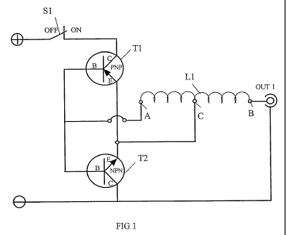
Figure 1 shows the circuit of a first embodiment of
the converter f ormingthe subject of the invention comprising
a first transistor, a second transistor, and an inductor,
where the output for the load is located between one end
of the inductor and the collector of the second transistor;
Figure 2 shows the circuit of Figure 1 upon closing
of the switch, where a first transistor is active and a second
transistor is inhibited;
Figure 3 shows the circuit of Figure 1, where the first
transistor is inhibited and the second transistor is active;
Figure 4 shows a first variant of the circuit of Figure
1, where the inductor is wound on a core of ferromagnetic
material or ferrite;
Figure 5 shows the circuit of Figure 4, where, as an
alternative to a switch, two pushbuttons are provided;
Figure 6 shows the circuit of a second embodiment of
the invention, where the output for the load is located-
between one end of the inductor and the collector of the
first transistor;
Figure 7, like Figures 4, shows a variant of the circuit
7
CA 02804426 2013-01-04
WO 2011/004406 PCT/IT2009/000296
of Figure 4;=
Figure 8, like Figure 5, shows the circuit of Figure
7, where as an alternative to a switch two pushbuttons are
provided;
Figure 9 shows the circuit of a third embodiment of
the invention, where two outputs are provided for a
corresponding load, a first output located between one end
of the inductor and the collector of the first transistor,
and a second output between the same end of the inductor
and the collector of the second transistor;
Figures 10-12 each show a variant of the circuit of
Figure 9;
Figure 13 shows a fourth embodiment of the circuit of
Figure 1, which comprises two inductors, which are the same
as one another, and one output, which is taken between said
two inductors and in which one end of the second inductor
is connected to the collector of the second transistor;
Figures 14 and 15 show, respectively, afifth embodiment
that comprises two inductors that are the same as one another,
and one output, which is taken between said two inductors
and in which one end of the second inductor is connected
to the collector of the second transistor, and a variant
thereof;
Figure 16 shows the circuit of a sixth embodiment, which,
unlike the circuit of the third embodiment of Figure 9,
envisages that the inductor is wound on a ring of
ferromagnetic material or ferrite;
Figures 17 to 20 each show a variant of the circuit
of Figure 16;
Figure 21 shows the circuit in a seventh embodiment;
Figures 22 to 25 each show a variant of the circuit
8
CA 02804426 2013-01-04
WO 2011/004406 PCT/IT2009/000296
of Figure 21=;
Figure 26 shows the circuit of an eighth embodiment;
and .
Figures 27 to 29 each show a variant of the circuit
of Figure 26.
With particular reference to Figures 1 to 3, in the
first embodiment described, the basic circuit of the
converter comprises:
a first transistor Ti of a PNP (or else NPN) type;
- a second transistor T2 of an NPN (or else PNP) type,
having the base and the emitter connected, respectively,
to the base and to the emitter of the first transistor Ti;
and
- a coil or inductor Ll having a first end A that is
to be connected to the bases of said two transistors Ti and
T2, a second end B that is free, and a common central zero
C, which divides said inductor into two equal portions and
is to be connected to the emitters of the transistors Ti
and T2;
wherein said circuit is supplied by a direct current applied
to the collectors of the two transistors Ti and T2 and
envisages at least one output, between said second end B
and the collector of one transistor Ti or T2, for connecting
a respective load Cl that is able to behave substantially
as a capacitor, such as for example an electroluminescent
cable or panel.
In the example described, the circuit envisages an
output OUT1, which is taken between the end B of the inductor
L1 and the collector of the second transistor T2.
The two portions of the inductor Ll, i. e. , the portion
from the end A to the central zero C and the portion from
9
CA 02804426 2013-01-04
WO 2011/004406 PCT/IT2009/000296
the latter to the end B, are preferably insulated from one
another at the central zero.
The transistors used in the circuit must always be
complementary, i.e., one of a PNP type and one of an NPN
type, in order to generate a voltage substantially equal
to 0 Von the connection between the bases of the transistors
themselves.
With reference to Figure 2, upon turning-on of the
circuit, for example by closing of a switch Si, the first
transistor T1 is activated whilst the second transistor T2
is inhibited. The current traverses the first transistor
T1 and traverses the inductor L1, in the portion from the
central zero C to the end B, until the load C1 is reached,
which, behaving substantially as a capacitor, is charged
until the maximum of the voltage envisaged is reached.
Once the load C1 has reached the maximum voltage
envisaged, the current ceases to traverse the transistor
T1 and the inductor L1.
At this point, the first transistor Ti goes into
inhibition, and across the inductor L1 an opposite current
is generated with respect to the initial one, which, however,
is not sufficient to activate the second transistor T2.
Thanks to the load C1, which has a positive voltage, a further
opposite current is generated, which adds to the opposite
current across the inductor L1 and enables activation of
the second transistor T2, whilst the load Ci starts to
discharge. In other words, the opposite current that
traverses the second transistor T2 and the inductor L1, in
the portion from the central zero C to the end A, activates
the second transistor T2 itself.
After the load C1 has been completely discharged, the
CA 02804426 2013-01-04
WO 2011/004406 PCT/IT2009/000296
inductor L1 reverses the polarity, and the load Cl, which
functions as capacitor, recharges, thus activating the first
transistor Ti and deactivating the second transistor T2 so
as to restore the situation that existed initially at the
moment of turning-on.
The cycle repeats until the circuit is deactivated,
and during this cycle the load Cl remains constantly lit
up.
According to a peculiar characteristic of the invention,
the voltage with which the load Cl is-supplied has a
practically perfect sinusoidal waveform, substantially
without any harmonics added to the carrier.
A second peculiar characteristic of the invention lies
in the fact that, when the supply is removed or the load
Cl is disconnected fromthe output of the circuit, the voltage
on the connection between the bases of the two transistors
Ti and T2 returns to a value of 0 V.
It should be noted that the operating frequency, i. e. ,
the alternating current that supplies the load Cl, is a
function of the electrical characteristics of the load Cl
and of the inductor L1, given that, as the capacitance of
the load C1 and/or the inductance of the inductor L1 increase,
the frequency decreases since the time necessary to reach
the maximum voltage envisaged increases, and vice versa.
The capacitance of the electroluminescent cable is
proportional to its length and diameter.
The capacitance of the electroluminescent panel is
proportional to its dimensions..
The circuit is supplied in direct current, and only
when the load Cl, which functions as capacitor, is connected
to the output of said circuit, does the inductor L1 start
11
CA 02804426 2013-01-04
WO 2011/004406 PCT/IT2009/000296
to oscillate, transforming the direct current into
alternating current in the form of a substantially perfect
sinusoidal signal, which supplies said load, which thus turns
on. In other words, in connecting the load Cl to the output
of the circuit, the circuit itself is closed, and the inductor
L1 co-operates with the capacitor that is constituted by
the -load Cl itself.
From the experimental data it has surprisingly been
found that, if the input of the circuit is connected to the
electrical supply but there is no load Cl connected to the
output of said circuit, the converter remains static: there
is in fact no absorption or dispersion of electrical energy.
It should be noted that if passive components are added
to the basic circuit described above, such as for example
resistors, the circuit will no longer respect its
characteristics of operation.
In addition to this, if for any external cause the
temperature of the load Cl and/or of the inductor Ll exceeds
a certain threshold, the converter is automatically
deactivated. On the one hand, when the temperature of the
load Cl exceeds a certain threshold, the load Cl itself no
longer charges and is unable to originate a potential such
as to generate an opposite current that is able to activate
one of the two transistors T1 and T2, each of which remains
in its current state. On the other hand, when the temperature
of the inductor L1 exceeds a certain threshold, the opposite
current decreases and it is no longer sufficient to switch
one of the two transistors Ti and T2, even though there is
the presence of the opposite current generated by the load
Cl.
The converter is automatically deactivated also in the
12
CA 02804426 2013-01-04
WO 2011/004406 PCT/IT2009/000296
case where there occurs a possible short circuit of the load
C1 (electroluminescent cable or panel) so as to safeguard
its supply source and its own components.
The same applies if a short-circuit of the
direct-current source occurs.
The inventive idea underlying the invention enables
provision of a converter for high and low powers limited
by the technical characteristics alone of the components.
This innovative converter according to the present
invention is preferably inserted in a,closed container made
of plastic material.
On the outside of the surface of the container there
can be provided:
- an on/off switch for activating said converter;
- an output plug for supplying the load, such as, for
example, a cable or a panel; and
- an input plug for the electrical supply of the device
itself.
As will emerge more clearly from what follows, it is
possible to add other components to the basic circuit as
illustrated in the drawings annexed hereto purely by way
of example.
In a variant illustrated in Figure 4, it is envisaged
that the inductor L1 is wound on a ferrite core F to increase
the inductance.
The circuit of said variant envisages as an alternative
to the switch Si two distinct pushbuttons: a first pushbutton
Z1 for turning on the circuit, set between the base and the
collector of the first transistor T1, and a second pushbutton
Z2 for turning off the circuit, set between the emitter and
the base of the first transistor Ti (Figure 5).
13
CA 02804426 2013-01-04
WO 2011/004406 PCT/IT2009/000296
In a second embodiment illustrated in Figure 6, the
output OUT2 of the circuit is taken between the second end
B of the inductor L1 and the collector of the first transistor
Ti.
In a variant of the second embodiment, illustrated in
Figure 7, the inductor L1 is wound on a ferrite core F.
Also in this case, the circuit of said variant, as an
alternative to the switch S1, can also envisage two distinct
pushbuttons: a first pushbutton Z1 for turning on the circuit,
set between the base and the collector of the first transistor
Ti, and a second pushbutton Z2 for turning off the circuit,
set between the emitter and the base of the first transistor
Ti (Figure 8).
In a third embodiment illustrated in Figure 9, the
circuit has two outputs: a first output OUT1 set between
the second end B of the inductor L1 and the collector of
the second transistor T2, and a second output OUT2 set between
the second end B of the inductor L1 and the collector of
the first transistor T1.
Consequently, said circuit offers the possibility to
the user of connecting a respective load to one or both of
the outputs.
It should be pointed out that each of said loads must
behave substantially as a capacitor.
In this specific case, the sinusoidal waveform
generated by the circuit will supply the loads connected
to the outputs.
In a variant of this third embodiment, illustrated in
Figure 10, the switch Si is replaced by two distinct
pushbuttons Z I and Z2, respectively located between the base
and the collector of the first transistor Ti and between
14
CA 02804426 2013-01-04
WO 2011/004406 PCT/IT2009/000296
the emitter and the base of the first transistor Ti.
In a secondvariant of the third embodiment, illustrated
in Figure 11, it is envisaged that the inductor L1 is wound
on .a ferrite core F.
The circuit of said variant can also envisage, as an
alternative'to the switch Si, two distinct pushbuttons Z1
and Z2 as in the first variant (Figure 12).
In a fourth embodiment illustrated in Figure 13, the
circuit comprises, instead of the inductor L1, two inductors
that are the same as one another:
a first inductor Lll'having a first end A that is
to be connected to the bases of the two transistors T1 and
T2, and a second end C11 that functions as central zero that
is to be connected to the emitters of the two transistors
T1 and T2; and
- a second inductor L12 with a first end C12 that is
free and a second end B that is to be connected to the,collector
of the second transistor T2;
wherein said circuit envisages an output OUT10 between said
first end C12 of the second inductor L12 and the second end
C11 of the first inductor L11.
A fifth embodiment illustrated in Figure 14 differs
from the preceding one in that the second end B of the second
inductor L12 is connected to the collector of the first
transistor T1.
A first variant of said fifth embodiment, illustrated
in Figure 15, envisages that said two inductors L11 and L12
are wound on a ferrite core F and that the switch Si is replaced
by two distinct pushbuttons Z1 and Z2, respectively, for
turning on and turning off the circuit.
It is also possible to envisage that each of said
CA 02804426 2013-01-04
WO 2011/004406 PCT/IT2009/000296
inductors is *each wound on a respective ferrite core (not
illustrated in the figures).
In a sixth embodiment illustrated in Figure 16, as an
alternative to the inductor L1, two inductors are provided,
each of which is wound on a corresponding portion of a ferrite
ring AF: a first inductor Vl having a first end A connected
to the bases of the two transistors T1 and T2 and a second
end C, which, being connected to the emitters of the two
transistors T1 and T2, functions as common central zero,
and a second inductor V2 having a first end B that is free
and a second end connected to the end C of the first inductor
V1, i.e., to the central zero.
The circuit of said embodiment envisages at least one
output for the connection of a load C1 and a switch S1 of
a known type.
In the example described, the output designated by OUT1
is provided between said free end B of the second inductor
V2 and the collector of the second transistor T2.
In other words, this sixth embodiment differs from the
first embodiment in that the two portions of the inductor
L1 are wound on two opposite sides of the ferrite ring AF.
In a variant illustrated in Figure 17, the switch S1
is replaced by two distinct pushbuttons Z1 and Z2,
respectively for turning on and turning off the circuit.
In a second variant illustrated in Figure 18, the
circuit envisages an inductor L3 wound on a ferrite core
F set between the end B and the output OUT1.
The circuit of said variant can envisage, as an
alternative to the switch S1, two distinct pushbuttons Z1
and Z2, respectively for turning on and turning off the
circuit (Figure 19).
16
CA 02804426 2013-01-04
WO 2011/004406 PCT/IT2009/000296
In a further. variant of the sixth embodiment,
illustrated in Figure 20, the circuit envisages an inductor
L3 without ferrite core set between the end B and the output
OUT1, and an inductor L5 wound on a ferrite core F set between
the collector of the second transistor T2 and the output
OUT1.
The circuit of a seventh embodiment envisages, unlike
the circuit of the preceding embodiment, an output OUT2
between the free end B of the second inductor V2 and the
collector of the first transistor T1 (Figure 21).
In a first variant of said embodiment, the switch Si
is replaced by two distinct pushbuttons Z1 and Z2,
respectively for turning on and turning off the circuit
(Figure 22).
In a second variant, set between the free end B of the
second inductor V2 and the output OUT2 is an inductor L6
wound on a ferrite core F (Figure 23).
The circuit of said variant can envisage, as an
alternative to the switch S1, two distinct pushbuttons Z1
and Z2, respectively for turning on and turning off the
circuit (Figure 24).
Said circuit can also be modified in such a way that
the inductor L6 is without the ferrite core, and s.et between
the collector of the first transistor Ti and the output OUT2
is an inductor L7 wound on a ferrite core F.
An eighth embodiment illustrated in Figure 26 differs
from the sixth embodiment in that a second output OUT2 is
provided between the end B and the collector of the first
transistor Ti.
In a first variant illustrated in Figure 27, the switch
Si is replaced by.two distinct pushbuttons Z1 and Z2,
17
CA 02804426 2013-01-04
WO 2011/004406 PCT/IT2009/000296
respectively for turning on and turning off the circuit.
In a second variant illustrated in Figure 28, the
circuit envisages a first inductor L9 set between the end
B and the output OUT1, a second inductor L10 wound on a ferrite
core F set between the collector of the second transistor
T2 and- said output OUT1, and a third inductor L11, which
is also wound on a ferrite core F, set between the collector
of the first transistor T1 and the second output OUT2.
In a further variant illustrated in Figure 29, the
switch S1 is replaced by two distinct pushbuttons Z1 and
Z2, respectively for turning on and turning off the circuit.
In the examples of embodiment described so far, it is
advantageously possible to apply to the circuit a d.c.
voltage that ranges from a minimum value of 0. 050 mV up to
a maximum value pre-set by the manufacturer.
Advantageously, as already mentioned, the circuit
generates, starting from a direct current, an alternating
current having a substantially perfect sinusoidal waveform
that supplies a load having a behaviour similar to that of
a capacitor, such as an electroluminescent cable or panel;
said load in turn, thanks precisely to the fact that it is
supplied by said waveform, has a brightness higher than the
one that can be obtained with inverters of a known type with
a= consumption reduced by more than 50% as compared to that
of known inverters.
As the electrical power that it is desired to supply
to the electroluminescent cable or panel varies, the
inventive idea underlying the invention does not change,
but only the power levels and the dimensions of the components
are modified as a function of the length of the cable or
the dimensions of the panel.
18
CA 02804426 2013-01-04
WO 2011/004406 PCT/IT2009/000296
The present invention has been described and
illustrated in some preferred embodiments and variants
thereof, but- it is evident that the person skilled in the
sector may. make technically equivalent modifications and/or
replacements thereto, without thereby departing from the
sphere of protection of the present industrial patent right.
For example, it is possible to envisage, as an alternative
to the bipolar junction transistors (BJTs) , as the ones used
in the circuits described so far, transistors of a MOSFET
or JFET type, provided that they are complementary to one
another. It is also possible to envisage the addition of
further pairs of complementary transistors to be connected
in series or in parallel to the pair of transistors present
in the circuit or also to envisage the addition of further
inductors to be connected in series or in parallel to the
inductor or inductors of the circuit.
19