Note: Descriptions are shown in the official language in which they were submitted.
CA 02805814 2015-04-24
CA2805814
1
METHOD AND APPARATUS FOR SENSING A PROPERTY OF A FLUID
FIELD OF THE INVENTION
The present invention relates to methods and apparatus for sensing a property
of a fluid. In
particular, the invention provides coordination of sensors in a microfluidic
environment.
BACKGROUND
Devices that integrate one or several functions on a single chip have many
applications such as
monitoring a property of a fluid or a chemical reaction. Such devices, known
as lab-on-chip devices,
typically combine semiconductor sensors and microfluidic channels on a tiny
scale.
However, there is a requirement for low-cost integration of different
technologies, in particular
CMOS/MEMS and microfluidics. Economies-of-scale especially driven by the
semiconductor
industry favour solutions based on unmodified commercial processes. The
constraints dictated by
the varying range of physical dimensions of the different components make
wafer-level integration
too costly for low-cost mass manufacture. For example, a typical Lab-on-Chip
application may
require CMOS components having an area in the region of 1-10mm2, MEMS
components in the
region of 25-100mm2 and microfluidics components in the region of 200-2500mm2.
Therefore
integrating these at wafer level would be hugely wasteful to CMOS/MEMS
technologies, as the
common Lab-on-Chip area would be dominated by the requirements of interfacing
fluids and
external systems to the devices.
In known hybrid CMOS/microfluidic composites having encapsulated bond-wires
and die, problems
arise in wire-bonding the fine bond wires and the need to encapsulate them
afterwards.
Encapsulating chips at die level typically requires depositing and processing
photosensitive
materials (such as certain epoxies and SU-8) onto composite assemblies (such
as a package or
substrate), which are wire-bonded to the die. A common challenge is to avoid
damage to delicate
CA 02805814 2015-04-24
CA2805814
2
bond-wires due to mechanical stress caused by fluid viscosity in addition to
centrifugal forces in
spin-coating. An alternative approach is to define the unexposed (i.e.
chemical sensitive) area via a
sacrificial material (eg. SU-8), or by accurately defining a frame and then
potting the region
between the frame and package using a UV-curable epoxy. This technique is
often referred to as
"Dam and Fill" encapsulation. Commercial chemical sensors use more complex
process flows
based on combining the above techniques with pre-fabricated housings to ensure
robust isolation in
addition to long-term stability. However these are very laborious and thus
expensive to mass-
produce. All these above-mentioned techniques however have two fundamental
limitations: (i) an
unwanted well (typically 200-300pm depth) is formed inside the bondpad
regions, and (ii) due to
this relatively thick encapsulant build-up, the top surface is not perfectly
planar. This causes
sealing, adhesion, and alignment problems when overlaying microfluidic
channels above, which
often requires an intermediate levelling step.
Several technology-based packaging solutions have been proposed. However these
typically
require post-processing CMOS devices at wafer scale (i.e. before dicing). Flip-
chip packaging
methods can provide a robustly encapsulated, planar top surface, however the
issue of "parasitic
wells" above the chip surface is not overcome. The MIT/Lincoln Labs
experimental 3D CMOS
process based on multiple Silicon-on-Insulator (801) CMOS tiers allows for
through-tier vias and
since the silicon sits on an insulating substrate, the bondpads can be brought
to the underside of
the substrate, leaving the top-layer planar for chemical sensing purposes.
This perhaps offers the
most promising solution for future emerging technologies (expected to feature
towards the end of
Moore's law- when scaling from 22nm to 1 Onm). This is confirmed by IBM
dedicating a complete
issue to 3D CMOS in their flagship "IBM Journal of Research & Development".
However, this
technology remains years from being commercially available, and even then is
expected to remain
relatively expensive (compared to bulk CMOS) and thus it will be limited to
niche applications.
Once the sensor has been encapsulated, it is desirable to provide a
microfluidic channel to bring
the fluid to the sensor. These channels are typically formed in a substrate,
which is separate from
the sensor substrate. The two substrates are aligned and sealed to each other.
As semiconductor
sensors become progressively smaller with a finer pitch, there arise problems
with aligning the
microfluidic channels to the sensors. Poor assembly tolerances mean that there
is a chance that
the walls between the channels may obstruct a sensor and indeed there may not
be a sensor in
CA 02805814 2015-04-24
CA2805814
3
each channel. In mass production, microfluidic alignment tolerances may be 100-
1000 times more
than the minimum feature size of the sensor.
In some applications it may be desirable to monitor reactions in a number of
fluidic chambers using
ISFET sensors. It is desirable to pattern a number of ISFET sensors on a
single silicon chip, and
yet have different reactions happen above each sensor. This means that the
surface of the chip
must be encapsulated in such a way as to create multiple chambers which are
fluidically sealed
from each other so that their chemical components cannot intermix.
To provide a seal between sensors, it is expected that a layer of fluidic
channels/chambers will be
mounted on top of the electronic chip. This could be built or etched directly
on the surface of the
chip with photolithography, or alternatively could be built as a separate part
via a variety of means
and then attached to the chip as a subsequent step.
Either way, an apparent trade-off is created as the fluidic channels/chambers
must be aligned to
the sensors. There is incentive to make the sensors closely spaced, i.e. fine-
pitched, to minimise
the size and therefore cost of the silicon chip (and fluidics as well).
However, there is a competing
incentive to make the sensors further apart so that it is simpler to produce
the fluidics and align
them with the sensors.
Substrates are often aligned by either aligning one substrate to a datum line
on the other (perhaps
a physical protrusion) or by aligning visually overlapping marks on each
substrate. The intention is
that the two substrates are centre aligned or normally aligned, such that the
chambers and sensors
are symmetrically aligned about a centre line(s). This usually means that the
midpoint of each
sensor is aligned to the midpoint of each chamber. Thus the alignment
tolerance from centre is
usually the width of the chamber less the sensor width, after which point a
portion of the sensing
surface will not be exposed to the chamber. The alignment tolerance may be
expressed as:
Tolerance = (Wc- Ws)/2 (1)
Where Wc,Ws represent respectively the Width of one chamber, Width of one
sensor.
CA 02805814 2015-04-24
CA2805814
4
The following references provide background to lab-on-chip packaging:
US Patent 7,033,910: Method of fabricating multi layer MEMS and microfluidic
devices on a
substrate with layers of predetermined weak and strong bond regions,
communication provided by
edge interconnects between layers
US Patent 6,910,268: Method for fabricating an IC interconnect system
including an in-street
integrated circuit wafer via. Not wireless, uses wired vias.
US Patent 7,207,728: Optical bond-wire interconnections and a method for
fabrication thereof.
Optical bond-wire interconnections between microelectronic chips, wherein
optical wires are
bonded onto microelectronic chips.
US Patent 6,443,179: Packaging of electro-microfluidic devices. Electrical
connection is made to
bond pads on the front of the MIC.
US Patent 6,531,342: Method for transverse hybrid loc package
US Patent 6,882,033: High density direct connect LOC assembly
US Patent 6,136,212: Polymer-based micro-machining for microfluidic devices
(WO/2003/107043) OPTOELECTRONIC ASSEMBLY WITH EMBEDDED OPTICAL AND
ELECTRICAL COMPONENTS.
IPC8 Class: AHO5K714FI, USPC Class: 361796: Interconnection and Packaging
Method for
Biomedical Devices with Electronic and Fluid Functions
E. Culurciello et. Al, "Capacitive Inter-Chip Data & Power Transfer for 3-D
VLSI", IEEE TCAS-II,
Vol. 53, No. 12, 2006.
T. D. Strong, "Integrated Electrochemical Neurosensors", IEEE ISCAS'06, pp.
4110-4113, 2006.
W. OeBrier, et al., "Encapsulation of ISFET sensor chips", Sensors & Actuators
B, Vol. 105, pp.
104-117, 2005.
L. Sudakov-Boreysha et al., "ISFET CMOS Compatible Design and Encapsulation
Challenges",
IEEE Conference on Electronics, Circuits and Systems (ICECS'04), pp. 535-538,
2004.
"3D Chip Technology", IBM Journal of Research and Development, Vol. 52, No. 6,
2008.
Vilches A, Sanni A, Toumazou C, Single coil pair transcutaneous energy and
data transceiver for
low power bio-implant use, IET ELECTRONICS LETTERS, 2009, Vol:45, Pages:727-
U25,
ISSN:0013-5194.
CA 02805814 2015-04-24
= CA2805814
SUMMARY
According to a first aspect disclosed herein there is provided a device for
sensing a property of a
5 fluid, the device comprising a first substrate having formed thereon a
sensor configured in use to
come into contact with a fluid in order to sense a property of the fluid, and
a wireless transmitter for
transmitting data over a wireless data link; and a second substrate having
formed thereon a
wireless receiver for receiving data transmitted over said wireless link by
said wireless transmitter.
The first substrate is fixed to or within said second substrate.
According to a second aspect of this disclosure, there is provided a method of
operating one or
more sensors and comprising the steps of providing a fluid in contact with a
sensor, powering the
sensor and transmitter using a transducer, sensing a property of the fluid
using the sensor, and
wirelessly transmitting sensed or processed sensed data using a transmitter.
According to a third aspect of this disclosure, there is provided a method of
fabricating a
microfluidic sensor device comprising the steps of providing a first substrate
defining one or more
microfluidic structures for receiving a fluid to be sensed, providing a second
substrate comprising or
having attached thereto a multiplicity of fluid sensors, the number of sensors
being greater than the
number of microfluidic structures, and fixing the first and second substrates
together such that at
least one of the sensors is aligned with the or each microfluidic structure so
as to provide an active
sensor for the or each structure, and such that one or more of the sensors is
or are not aligned with
any microfluidic structure and is or are thereby redundant.
According to a fourth aspect of this disclosure, there is provided a device
comprising a first
substrate defining one or more microfluidic structures for receiving a fluid
to be sensed and a
second substrate comprising or having attached thereto a multiplicity of fluid
sensors, the number
of sensors being greater than the number of microfluidic structures. The
second substrate is in
contact with the first substrate such that at least one of the sensors is
aligned with the or each
microfluidic structure so as to provide an active sensor for the or each
structure, and such that one
CA 02805814 2015-04-24
= = CA2805814
6
or more of the sensors is or are not aligned with any microfluidic structure
and is or are thereby
redundant.
According to a fifth aspect of this disclosure, there is provided a method of
configuring a device
and comprising the steps of (i) detecting a first signal corresponding to a
first sensor and (ii)
determining which sensors are exposed to which microfluidic structure using
the first signal and
knowledge of a property of the fluid of at least one microfluidic structure or
knowledge of the spatial
relationship among the sensors.
According to a sixth aspect of this disclosure, there is provided a
configuration apparatus for
configuring a device, the configuration apparatus comprising (i) a receiver
for detecting a first signal
corresponding to a first sensor and (ii) means for determining which sensors
are exposed to which
microfluidic structure using knowledge of a property of the fluid in at least
one of the microfluidic
structures or knowledge of the spatial relationship among the sensors.
The invention claimed herein relates to a method of fabricating a microfluidic
sensor device
comprising the steps of: providing a first substrate defining one or more
microfluidic structures for
receiving a fluid to be sensed; providing a second substrate comprising or
having attached thereto
a multiplicity of fluid sensors, the number of sensors being greater than the
number of microfluidic
structures; and fixing the first and second substrates together such that at
least one of the sensors
is aligned with each microfluidic structure so as to provide an active sensor
for each structure, and
such that one or more of the sensors is or are not aligned with any
microfluidic structure and is or
are thereby redundant.. The fluid may be a biological or chemical sample to be
monitored or
detected. Also claimed is a method of configuring such a device comprising the
steps of: (i)
detecting a first signal corresponding to a first sensor; and (ii) determining
which sensors are
exposed to which microfluidic structure using the first signal and knowledge
of a property of the
fluid of at least one microfluidic structure or knowledge of the spatial
relationship among the
sensors. Also claimed is configuration apparatus for configuring such a
device, the apparatus
comprising: (i) a receiver for detecting a first signal corresponding to a
first sensor; and (ii) means
for determining which sensors are exposed to which microfluidic structure
using knowledge of a
property of the fluid in at least one of the microfluidic structures or
knowledge of the spatial
relationship among the sensors.
CA 02805814 2015-04-24
= CA2805814
7
Particular embodiments are set out in the accompanying dependent claims.
DESCRIPTION OF DRAWINGS
Specific embodiments of the invention will now be described by way of example
only, with
reference to the accompanying figures, in which:
Figure 1 illustrates a known CMOS encapsulation method for chemical sensing;
Figure 2 is a cross-section of a microfluidic assembly with a CMOS sensor
embedded within a
substrate;
Figure 3 illustrates an embodiment providing data transfer using optical (IR)
communication;
Figure 4 illustrates an embodiment providing data transfer using local
inductive coupling;
Figure 5 illustrates an embodiment providing data transfer using RFID
technology;
Figure 6 illustrates a two-dimensional array of fluid chambers overlaying a
two-dimensional array of
ISFETs; and
Figure 7 illustrates a one-dimensional array of fluid chambers overlaying a
one-dimensional array of
ISFETs.
DETAILED DESCRIPTION
Figure 1 shows a cross-section of a known hybrid CMOS/microfluidics composite
having bond-
wires 10 and die 4 encapsulated using photo-patternable epoxy 2. The
microfluidic chamber 11 is
formed by the substrate 1 being fixed to the carrier substrate 8.
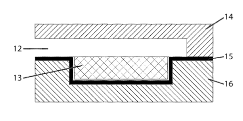
In one embodiment of the present disclosure as illustrated by Figure 2, a
semiconductor sensor
chip 13 is encapsulated by adhesive 15 within a recess of substrate 16. This
leaves the sensing
surface of the chip co-planar with the chamber 12. A second substrate 14 is
sealingly fixed to the
substrate 16 and provides microfluidic channels for the fluid to be sensed.
Fluid may be brought into contact with the sensing surface of chip 13 and
detected. Properties
such as temperature, pH, chemistry, flow conductivity, etc. may be detected by
an appropriate
sensor integrated into the chip. By providing suitable wireless
CA 02805814 2013-01-17
WO 2012/017185 PCT/GB2010/051299
8
communication and transducer hardware on the CMOS chip, a scheme for
contactless
power and data transfer can be implemented. The chip is thus capable of
wirelessly
transmitting a signal to a receiver located nearby. The signal contains data
relating to
the state of the chip or a property of the fluid via the sensor.
The embodiment thus provides a method of encapsulating and interfacing a
sensor
chip to a device without any bond-wires leaving the chip's top surface planar.
A transducer is a device for transforming energy from one form to another. For
example, a circuit may receive incident radiated energy and transform it into
a DC
electrical power. In such a way power may be transmitted wirelessly.
Wireless communication refers to communication amongst two or more devices
without
the use of electrically conducting wires, as is typical of conventional
communication
methods. The transmission of wireless communication may be provided by
energizing
a signal which emanates from the transmitter or modulating an energized signal
passing near or through the transmitter to create a new signal. The signal
contains
coded or uncoded data that can be interpreted by a receiver. The communication
may
be two-way in which case each device is configured to transmit and receive
signals (a
transceiver). A first device may produce a energy burst to request data (by
polling or
'pinging') from a second device such that the second device then transmits
data.
A wireless scheme may be applied to a Lab-on-Chip (LOC) assembly by
implementing
the following design steps:
= Fit a CMOS die within a recess of a (carrier) substrate, which may be a
multi-
layer printed circuit board (PCB), such that the top surfaces of the die and
(carrier) substrate are co-planar (see Fig. 2).
= Stack a microfluidic substrate onto the carrier substrate. These can be
designed
to be of equal dimensions (i.e. length and width), to form a 2-layer assembly
(see Fig. 2).
CA 02805814 2013-01-17
WO 2012/017185 PCT/GB2010/051299
9
= Provide a communication subsystem and transducer on the CMOS chip to
recover power and data from an external source, in addition to being able to
transmit data off-chip.
= Provide suitable structures, for example, PCB patterned antennas or
inductors
into the (carrier) substrate or sub-miniature surface mount (chip) components
(depending on the wireless technique chosen) embedded within the carrier
substrate.
= Provide a ground plate on the underside (obverse of the sensing surface)
of the
die which contacts a ground plate of the substrate for the purpose of
providing
an electrical ground for the die. The contacts may be bonded together by
electrically conducting epoxy, which also serves to mechanically couple the
die
to the substrate.
Such a device has advantages of reliability, cost reduction, and ease of
assembly.
A wireless sensor system arrangement alleviates the requirement for wire-
bonding thus
providing substantial cost benefits for mass manufacture. In addition to
direct savings
relating to wire-bond processing, additional processing steps are saved, for
example
bond-wire encapsulation and surface levelling steps. As the encapsulant around
the
bond wires is typically the first component to degrade when immersed in an
electrolyte,
the stability and reliability of the chip are also improved. The semiconductor
chip itself,
which requires expensive material and processing, may be much smaller than
before
as no space is required for bonding or encapsulation. The chip may be as small
as the
sensor and communication hardware.
Simplifying the process flow alleviates the requirement for time-intensive
high precision
alignment tasks. This means the various components can be manufactured to
utilise
inexpensive mass production techniques, for example injection moulding and
robot
assembly. Assembly alignment issue are reduced because the sensor chips may be
dropped directly into the microfluidic chambers (which is physically larger
than the chip
itself) without the need to align the substrates exactly. There may be many
chambers
formed in a substrate, with one or more chips located within each chamber.
CA 02805814 2013-01-17
WO 2012/017185 PCT/GB2010/051299
This method avoids the formation of parasitic wells formed within encapsulated
dies
(via traditional methods). This simplifies the microfluidic channel design, in
addition to
providing a means for robust substrate integration due to inherently planar
substrates.
5 Figure 1 identifies the following components:
1. Microfluidic substrate
2. Encapsulant
3. Bondpad (on chip)
4. Die (i.e. chip)
10 5. Silicon substrate
6. Dielectric/Passivation
7. Parasitic microfluidic well
8. Carrier substrate (e.g. PCB)
9. Bondpad (on carrier substrate)
10. Bondwire
11. Microfluidic channel
Figure 2 identifies the following components:
12. Microfluidic channel
13. Die (i.e. chip)
14. Microfluidic substrate
15. Adhesive/encapsulant
16. Carrier substrate (e.g. PCB)
Figure 3 identifies the following components:
17. Carrier substrate (e.g. PCB)
18. Light emitter
CA 02805814 2013-01-17
WO 2012/017185 PCT/GB2010/051299
11
32. Light detector
33. Reflector (e.g. sheet of interconnect metal)
34. Silicon substrate
35. Reflected light path
36. Optical modulator
37. Die (i.e. chip)
Figure 4 identifies the following components:
19. Inductive coupling
20. Inductor on carrier substrate
21. Inductor on chip
28. Carrier substrate (e.g. PCB)
29. Silicon substrate
30. dielectric stack/interconnects
31. Die (i.e. chip)
Figure 5 identifies the following components:
22. Die (i.e. chip)
23. Antenna on chip
24. Silicon substrate
25. Antenna on carrier substrate
26. Carrier substrate (e.g. PCB)
27. RF communication
Figures 3 to 5 illustrate embodiments for achieving power and data transfer
(between
the CMOS die and the substrate), replacing physical wire bonds with wireless
methods.
The figures illustrate: (Figure 3) use of an optical emitter from the
underside to power
CA 02805814 2013-01-17
WO 2012/017185 PCT/GB2010/051299
12
the device and use of electro-optical techniques to modulate the reflected
signal;
(Figure 4) an inductive power/data transfer between on-chip and PCB inductors;
and
(Figure 5) use of RF wireless technology.
The wireless power/data transfer can, for example, be achieved using the three
following techniques:
Optoelectronic transmission: Optoelectronics is the application of electronic
devices
that source, detect and control light, for example by absorption and
modulation of
optical energy. By embedding the integrated circuit within a substrate that
incorporates
suitable optoelectronic components, power can be transmitted to the integrated
circuit
(IC) and data received from it, providing the appropriate hardware is
integrated within
the IC. More specifically this would require integrating a solar cell to
recover optical
power, in addition to an optical emitter or modulator for transmitting the
sensor data.
One method of achieving the latter is by modulating free-carrier absorption
through
reverse biasing a pn-junction (see UK patent application 1001696.2 ). This
scheme is
illustrated in Fig. 3. The carrier substrate (17) houses an optical emitter
(18), optical
detector (32) and integrated circuit (37). By irradiating a modulator (36)
designed within
the bulk silicon (34), the resulting beam of light (35) can be modulated by
adjusting the
absorption within the modulator. The resulting beam can be reflected to the
underside
of the IC using a metallic reflector (33). This additionally acts to double
the modulation
effect (by modulating the light twice- the incident and return path).
Near field: Near field wireless transmission techniques work over distances
comparable
to, or a few times the diameter of the device(s), and up to around a quarter
of the
wavelengths used. Near field transfer is usually magnetic (inductive), but
electric
(capacitive) energy transfer can also occur.
Power and data can alternatively be transmitted wirelessly through inductive
coupling
between an on-chip inductor and patterned inductor embedded within the carrier
substrate. This is illustrated in Fig. 4. The integrated circuit (31)
incorporates the
sensor, interface electronics and integrated inductor (21). The integrated
inductor is
CA 02805814 2013-01-17
WO 2012/017185 PCT/GB2010/051299
13
designed using appropriate geometries of metallic interconnects (30) within
the chip.
This is inductively coupled (19) to a secondary inductor (20) embedded within
the
carrier substrate (28) designed such as to maximize the coupling efficiency
(e.g. in
close proximity, matched quality factors, etc.). The integrated circuit (31)
and carrier
substrate (28) are also required to include all necessary components to
facilitate the
inductive transfer of power and data via standard circuit topologies.
Far Field: Far field methods achieve longer ranges, often multiple kilometre
ranges,
where the distance is much greater than the diameter of the device(s). With
Electo-
Magnetic propagation, signals may be transmitted from multiple integrated
circuits
within a single carrier substrate employing far-field (e.g. traditional RF)
transmission of
power and data. Within each integrated circuit (22), an integrated antenna
(23) is
included in addition to a standard RF transceiver circuit. The carrier
substrate (26)
includes an embedded antenna (25) which is shared by all IC's by transmitting
a carrier
wave from the substrate antenna (25), receiving this on the integrated
antennas (23)
and rectifying the AC signal to recover a DC power supply. Data is transmitted
from the
independent chips back to the carrier by implementing on-chip RF transmitters.
Multiple
channels (for multiple chips) can be multiplexed by using standard RF
communication
techniques (time-division, frequency division, etc. multiplexing). The system
can either
use a shared set of antennas for power and data transmission or separate
elements to
improve the efficiency of each task (i.e. power and data transfer).
Thru-Fluid Propagation: A signal can be transmitted through the fluid. It is
well-known
that a water solution which includes salt, or any other effective electrolyte,
acts as a
conductive medium, and therefore can be used to send information on the same
principle as a wire. One illustrative implementation is to have a chip with an
integral
electrode (e.g. silver / silver chloride or other means) which contacts the
fluid, allowing
the circuitry on the chip to interface with the potential of the fluid and/or
vice-versa. A
second electronic module in communication with the chip would also have an
electrode
contacting the same electrolyte. Any voltage or voltage change driven by an
electrode
on either module would be conducted to the other module by the fluid, thereby
influencing the other electrode being measured at the receiver. In this way,
voltage
changes could act as a signal for analogue or digital information to be sent
between the
modules via the potential of the fluid. An alternative to direct electrode
contact is to
CA 02805814 2013-01-17
WO 2012/017185 PCT/GB2010/051299
14
capacitively-couple the chip to the fluid (for example, if a metal trace in
the chip was
separated from direct contact with the fluid by chip passivation) or by other
non-contact
means.
Further, if it is desirable for the fluid to also act as a stable DC bias (as
in the case of a
potentiometric measurement), then the circuitry, electrodes, and or signals,
can be
designed such as to only affect the potential of the fluid within a particular
frequency
range which does not interfere with the DC bias. Generally, having a non-zero-
impedance coupling between the electrode and the fluid, or between the driving
circuit
and the electrode, in at least one frequency band, is one way to ensure that
the driving
circuit can influence the fluid's potential without completely excluding the
influence of
other sources. This would enable 2-way communication, or multiplexing of
multiple
sources (e.g. via different frequency ranges or many other known techniques
for
multiplexing RF signals). One such implementation would be to have a capacitor
in
series between the driving circuit and the reference electrode in order to act
as a high-
pass filter, allowing the DC potential to be set externally by a reference
electrode or
any other module in the system (which correspondingly may have a low-pass
filter with
non-zero source impedance at some frequencies in its driving circuit to allow
the
electrolyte's potential to be driven at relatively higher-frequency for data
communication). Another enhancement would be for the chip to connect both
driving
and receiving circuits to its electrode via non-zero and non-infinite
impedances, such
that both send and receive functions are possible. Tr-state buffers can be
used to
further eliminate the influence of the driving circuit when not desirable.
The above embodiments differ from prior art wireless devices in several
respects:
= The wireless elements are all combined in a monolithic integrated circuit
(IC),
as opposed to being implemented using one or more discrete components (eg.
off-chip antenna, inductor, etc.
= The integrated circuit (IC) contains no bondpads or bondwire connections,
whereas other devices are wireless in one aspect but still rely on bondwires
in
other aspects, for example between the chip and package for power supply or
off-chip discrete components.
CA 02805814 2013-01-17
WO 2012/017185 PCT/GB2010/051299
= The transmitter and receiver communicate wirelessly whilst being
physically
connected. The distance between them is also predetermined and substantially
fixed. Typically the reason for using wireless technology is because the
transmitter and receiver are physically separated and occupy positions that
5 change or are unknown.
In one embodiment, a fluid is introduced into a chamber of the device and
brought into
contact with the sensor surface. The sensor is used to detect a property of
the fluid or
monitor a reaction within the fluid. This property may be the temperature or
ion
10 concentration. The carrier substrate may be constantly powering the
device and/or
waiting to receive a signal. The chip could transmit the present sensor value,
possibly
after performing signal processing. Alternatively the substrate would transmit
power at
a desired time which would power up the sensor chip. The chip may send the
signal
immediately or wait until it receives a request for the signal. For example,
there may
15 be several sensors monitoring separate fluids and the device could poll
or ping the
individual sensors at predetermined times.
The power transmitter, signal transmitter, and signal receiver may be formed
on the
same substrate or separated. For example the substrates may be plugged as a
cartridge into an In Vitro Device having circuitry which receives, analyses,
and displays
the sensor value.
Preferably the chip is monolithic comprising the sensor(s), transducer, and
transmitter
circuitry. Therefore there is provided an integrated chip having no wires
between the
chip and a substrate.
In one preferred embodiment there is a chip in physical contact with and
wirelessly
communicating with a PCB substrate. The chip has:-
= A receiving coil with a tuning capacitor to impedance-match the
transmitting coil
and optimise the quality factor.
= An asynchronous rectifier to rectify the output of the receiving coil to
give a
stable DC output voltage (1.4 V with 0.1 V ripple).
CA 02805814 2013-01-17
WO 2012/017185 PCT/GB2010/051299
16
= A clock recovery circuit in the form of a phase-locked loop (PLL) which
comprises a voltage-controlled oscillator (VCO), a phase detector, and a loop
filter. This produces a clock signal synchronized with the transmitting
frequency.
= A BPSK demodulator which uses the aforementioned on-chip recovered clock
signal and the voltage across the receiving coil to produce the demodulated
bitstream.
The PCB substrate has a transmitting coil driven with a 60 V peak-to-peak
drive
voltage in the 2.4 GHz unlicensed band. The data is coded onto this voltage
using
binary phase-shift keying (BPSK) such that the driving amplitude, and hence
the power
transmitted to the chip, is constant
Data is transmitted from the chip to the PCB via the on-chip "receiving" coil
to the PCB
"transmitting" coil (i.e., there are no separate coils) . This is done via
load-shift keying
(LSK) in which the load the on-chip coil sees is changed. This causes the
current
oscillating in the PCB coil to change, which can easily be measured and
demodulated.
In a further embodiment, microfluidic structures are finely-spaced without
requiring fine
alignment, by building redundancy into the system by creating an array of
ISFETs
which are greater in number than the microfluidic structures themselves. Then,
within
wide tolerance in lateral alignment, the redundancy ensures that wherever each
microfluidic structure aligns during assembly, at least one ISFET will be
available at an
appropriate location to measure it. The ISFETs which align with the
microfluidic
structures are utilised and the ones that are buried under walls are not.
In an embodiment, illustrated by Figure 6a, an array of sensors 42 are fixed
to one
substrate, and a second substrate 40 comprising an array of microfluidic
chambers 41
is aligned and sealed to the first substrate. The sealing prevents fluids from
one
chamber entering another chamber. In order to provide a robust assembly
procedure,
there are more sensors than chambers, the sensor being arranged such that
relative
CA 02805814 2013-01-17
WO 2012/017185 PCT/GB2010/051299
17
misalignment of the two substrates still results in at least part of one
sensing surface
exposed to the fluid in each chamber.
As can be seen from Figure 6a, chambers 41a illustrate the case where chambers
are
well aligned with one whole sensor each. However the substrates may be
relatively
misaligned in the X and/or Y direction such that each chamber (indicated by
dashed
chambers 41b) is aligned with a different sensor, or portions of several
sensors.
The amount of movement permissible in the plane of the substrate will depend
largely
on the number of excess sensors and pitch of the sensors. In Figure 6a, the
sensor
pitch is equal to the width of the chamber allowing the greatest amount of
movement
whilst ensuring that each chamber is aligned with a whole sensor or portions
of several
sensors. This arrangement is suitable to sensors that do not require that the
entire
sensing surface be exposed to the fluid in order to make a measurement.
For sensors that require that the entire sensing surface be exposed to the
fluid, it will
be desirable to decrease the pitch of the sensors. As seen in Figure 6b, each
chamber
aligns with at least one whole sensor and possibly portions of additional
sensors. In this
arrangement it is possible to have a chamber aligned with 4 whole sensors, the
sensor
pitch arranged such that the sensor pitch plus one sensor width is less than
or equal to
the chamber width.
It is possible that in addition to alignment tolerance, one would consider the
manufacturing tolerances of the chambers or sensors. For example the chamber
array
may be irregularly spaced apart or have differing chamber widths. The
combination of
these tolerances should be considered when determining the sensor layout. In
particular, the alignment tolerance will affect the number of excess sensors
needed and
the manufacturing tolerance will affect the sensor pitch needed.
The array may be one dimensional (see Figure 7) or two dimensional (see Figure
6). In
Figure 7, the chambers are part of channels in which a fluid flows (as
indicated by the
vertical arrows 53). The fluid flow is perpendicular to the sensor array.
Movement in
CA 02805814 2013-01-17
WO 2012/017185 PCT/GB2010/051299
18
the Y-direction has no affect on the sensor-chamber relationship and movement
in the
X-direction results in a change in the sensor-chamber relationship accounted
for by the
excess of sensors.
In the embodiment illustrated in Figure 7, two chambers having a width (51) of
200um
and a pitch (54) of 400um, intersect a linear array of 50um-wide ISFETs having
a pitch
(52) of 150um. There are 9 sensors, providing an excess of 7 sensors. The
channels
need not be aligned better than 475um from the centre line (allowing a total
lateral
movement of 950um) to ensure a whole sensor is exposed to each chamber. Such a
tolerance is much improved over the typical device having a single, cantered
sensor
per chamber where the tolerance would be 75nm. However, by adjusting the
parameters, even finer channels could be aligned with even less precision. The
general expression for the tolerances given by:
Total_Tol = (Ns-1)*Ps-Ws-(Nc-1)*Pc+Wc (2)
Tol = Total_Tol / 2 (3)
where:
Wc, Ws Width of one chamber, Width of one sensor
Pc, Ps Pitch of chambers, Pitch of sensors
Ns, Nc Number of sensors, Number of chambers
Total_Tol, Tol Total allowable lateral movement, alignment tolerance in
each
direction from centre line
An advantage is that this technique decouples the competing priorities of high
sensor
density and simplicity of assembly, so that fine-pitch sensors and chambers
can be
employed to minimise chip cost without requiring expensive, fine-scale
assembly and
alignment.
Certain embodiments may include one or more of the following properties:
= the transverse separation distance between adjacent sensors surfaces is
less
than the width of chamber in that direction;
CA 02805814 2013-01-17
WO 2012/017185 PCT/GB2010/051299
19
= there is a greater number of sensors than number of chambers, preferably
10%
more or 2 more;
= there is a greater number of sensors than number of chambers, preferably
50%
more or 5 more;
= there is a greater number of sensors than number of chambers, preferably
100% more or 10 more;
= there is at least one sensor at least partly exposed to each chamber and
at
least one sensor is not wholly exposed to any chamber;
= the width of a chamber is greater than or equal to the pitch of the
sensors;
= the pitch of the sensors is less than the pitch of the chambers;
= the pitch of the chambers is twice the pitch of the sensors;
= the pitch of the sensors is less than width of the chambers plus the
width of the
sensors;
= the total width of the sensor layout is wider than the width of the
chamber
layout;
= one substrate is aligned to the other substrate within a predetermined
tolerance
depending on the number of sensors in excess of the number of chambers.
After assembly, it may be initially unknown as to which sensors are covered by
the
second substrate and which sensors are exposed and to which chamber. Similarly
it
may be initially unknown which wireless sensors are paired with which receiver
on the
substrate and located within which chamber The arrangement can become known
during an calibration step with controlled conditions to see which sensors
measurements are different from the rest. For example, exposed temperature
sensors
will detect the temperature of the fluid in the chambers whilst blocked
sensors will
detect the temperature of the substrate. A controlled temperature may be
introduced
into the substrate or one or more chambers to highlight the difference in
sensor
measurements. To select an active ISFET, one could change the potential or
composition of the fluid electrolyte and observe which ISFETs react. Those
that do not
react beyond a predetermined threshold are considered to be unexposed to the
fluid.
CA 02805814 2013-01-17
WO 2012/017185 PCT/GB2010/051299
In one embodiment, several wireless sensors communicate with a far field
transceiver
in the substrate and the identity of each sensor in each chamber is unknown. A
property of the fluid in each chamber is altered such that the fluids do not
all have the
same property in each chamber. For example, a heater in each chamber may be
5 turned on one at a time, or a temperature gradient across the chambers
may be
established. Alternatively an electrode exposed to the fluid may provide a
reference
voltage to be detected. The substrate transceiver requests a signal from a
particular
sensor. This can be repeated for each sensor. The signals of the sensors are
compared to each other or to the properties of each chamber fluid to determine
which
10 sensors are aligned with which chambers.
Some sensor arrangements will not require controlled conditions. For example,
some
sensors will output different signals depending on whether they are exposed to
a
chamber or to the second substrate.
In another embodiment, the relationship between sensors and chamber is
determined
from the known geometries of the sensor pattern (or substrate receiver
pattern) and
chamber pattern. Preferably, the signal of the sensor outermost in the array
is
observed first, moving progressively inwards to detect which is the first
signal exposed
to a chamber. For example, in Figure 6a, the bottom-leftmost sensor which
appears to
be active is determined to be aligned with the bottom-leftmost chamber, the
remaining
relationships becoming apparent after that. A sensor that is one chamber pitch
separated from a known active sensor is likely to be active as well.
In the case where more than one sensor is aligned with a chamber, several
active
signals from neighbouring sensors will confirm the location of the chamber.
The sensor
measurements may be used to calculate an average, detect a faulty sensor, or
provide
measurement redundancy. The plurality of sensors exposed to a chamber may also
provide spatio-temporal imagery.
The above calibration steps may be performed using software or hardware. The
results of the calibration may be stored in a look up table to identify active
sensors and
CA 02805814 2013-01-17
WO 2012/017185 PCT/GB2010/051299
21
their location for future signal processing. The steps may be performed as an
assembly step or during the initial operation of the lab-on-chip.
In the above discussions a fluid is exposed to the sensors by providing a
chamber for
containing the fluid. The skilled person will appreciate that other
microfluidic structures
may also provide an appropriate form for exposing the fluid to the sensors
such as a
channel for directing the fluid across the sensors, a well for holding a
fluid, or even a
simple substrate for receiving a droplet contained by surface tension. The
term
Thicrofluidic' generally refers to the manipulation of fluids that are
geometrically
constrained to a small, typically sub-millimetre, scale.
It should be appreciated that features described herein and illustrated in the
attached
drawings may be incorporated alone or in appropriate combination with other
features.
For example, different technologies for powering and transmitting signals may
be
combined to create a wireless sensing system.