Note: Descriptions are shown in the official language in which they were submitted.
CA 02806448 2013-01-24
1
Device for generating THz radiation with free electron beams
The present invention relates to a radiation source that makes use of the
emission of electromagnetic
THz-radiation from in vacuum free flOg electron beams.
Because there are several advantages using electromagnetic radiation with high
frequency several
approaches are known in the state of the art to achieve radiation in THz-
frequency.
Many of the frequencies and wavelengths of importance to the spectroscopy of
molecules and solid
bodies may be within the wavelength range extending from 3 mm to 30 pm from
100 gigahertz to 10
terahertz. The use of a micro-radiation source, which may be tunable within
the wavelength range and
implemented on a semiconductor chip of a wafer for this range of terahertz
radiation and which exhibits
sufficient power output within the range of between 1 pW and 1 W, may be
substantially significant from
a technical standpoint for spectroscopic applications in all areas of
environmental protection, analytics,
and in material characterization in military fields, medicine and biology, as
well as in chemistry and
physics. In addition such a miniaturized source is needed in building source
arrays for security applica-
tions like body-scanners and applications of array scanners using THz
radiation.
The terahertz range of the electromagnetic spectrum lies between the infrared
and radiofrequency re-
gions of the spectrum. Recent technological advances have allowed for
exploration of the possible ap-
plications within this region of the spectrum. The electromagnetic radiation
in the terahertz region has
many potential applications including medical imaging and security.
Terahertz spectroscopy can be used for detecting and identifying biological,
chemical and explosive
materials. The spectroscopic database in the terahertz range of the
electromagnetic spectrum is cur-
rently being compiled by labs throughout the world. In order to ensure safe
employment of terahertz
sources for such applications, the spectroscopy of biological materials and
the interaction of terahertz
CA 02806448 2013-01-24
2
frequencies with biological materials need to be studied in greater depth.
Data of terahertz interaction
with skin currently exists only from 0.1 to 2 THz.
The remaining portion of the terahertz spectrum ¨ 2 to 30 THz ¨ remains
unexplored. To enable the
fielding of terahertz sources in many groundbreaking applications, it is
necessary to further study the
terahertz portion of the spectrum. A terahertz source and spectrometer would
enable the biological re-
search necessary to better understand the interaction of terahertz frequencies
with biological tissue. The
requirements are for a tunable terahertz source capable of producing energy
from 0.1 to 7 THz at power
levels of 1 W, CW. It is of importance to develop and produce powerful,
tunable, affordable, and in addi-
tion miniaturized sources.
To generate certain frequencies in the far infrared range, coherent radiation
for example, molecular
lasers which are pumped by CO2 lasers may be used.
Other sources generate a THz pulse power using very high electron energies
e.g. several MeV ¨ Mil-
lions electron volts ¨ and wigglers, which are alternating solid state magnets
which force the electron to
wiggle around the axis and therefore emit electromagnetic radiation. Such
sources are called free elec-
tron lasers and can be used in special high energy physics institutes by
customers on a hourly basis for
very high cost. In search for a small, possibly portable THz source such
installations cannot be favored.
THz radiation sources of today use semiconductor diodes, so called GUNN
diodes, which allow several
GHz of oscillator frequency , disclosed in "H. Hartnagel et al. "Ballistic
electron waves swing (BEWAS)
to generate THz signal power", FREQUENZ Vol 63. Vol 3/4 (2009)60-62". This
radiation is then selected
by special filters to extract higher harmonics of the base frequency and use
this as "THz" i.e. 200 GHz
radiation, The extracted power from such diodes is in the p Watt regime. The
usable primary diode cur-
rent is limited by Joules heating. With the requirement for powerful sources
in the upper GHz and lower
THz regime, semiconductors cannot reach the goal. Currents in solid state and
current densities are
limited by Joules heating from the vibrating atomic lattice. This is a hard
wall for such devices.
Another way to generate coherent radiation in the far infrared range with a
higher power output is based
on the so-called Smith Purcell effect. It was proposed in S.J. Smith, E.M.
Purcell, Phys. Rev. 92, 1069,
(1953)", This new principle is based on the Smith Purcell effect, and uses a
free electron beam crossing
a metal grating to influence on this grating a vibrating surface charge which
emits coherently THz radia-
tion. The interaction of the DC primary beam with the standing emitted THz
wave leads to a bunching of
CA 02806448 2013-01-24
3
the beam and to an enhanced emission of the dipole radiation. It provides for
generating radiation simi-
lar to the method known from the "free electron laser". Macroscopic electron
sources and diffraction
gratings having a 100 to 300 pm period may be used to generate a coherent
radiation field of polarized
radiation having up to 1mW power. Such sources are also proposed in a
miniaturized form in the
US 6,909,104 A.
The reference "Intensity of Smith-Purcell Radiation in the Relativistic
Regime", J. Walsh, K. Woods, S.
Yeager, Department of Physics and Astronomy, Dartmouth College, Hanover, N.H.
03755, U.S., pages
277-279, discusses the theory of such Smith-Purcell radiation sources and,
additionally, gives experi-
mental results. The reference "A New Source of THz-FIR Radiation" in LEOS
NEWSLETTER, February,
1999 by J. E. Walsh, J. H. Brownell, J. C. Swartz, Department of Physics and
Astronomy, Dartmouth
College, Hanover, N.H. 03755-3528 and M. F. Kimmitt, Department of Physics,
Essex University, Col-
chester, UK, Jan. 7, 1999, pages 11-14, discusses the design and mode of
operation of a radiation
source in the terahertz region. The experiments showed the feasibility of the
approach disclosed in "M.
Goldstein, J.E. Walsh, M.F. Kimmit, J. Urata, C.L. Platt, Appl. Phys. Lett.
71, 452,(1997)". It may be that
these terahertz radiation sources are perfectly efficient, but they do not yet
suffice for many analytical
applications, and they are not yet miniaturized to a sufficient degree.
This effect is used and described in a miniaturized Smith Purcell THz-
radiation source
EP 1 186 079 B1.This source is miniaturized by using the EBID technology and a
self reproducing fabri-
cation technique with 3-dimensional direct deposition of the key structures,
as the electron emitter and
the miniaturized focusing optics, like it is disclosed in DE 10 302 794 A1.
It is to note that THz sources based on the Smith-Purcell effect suffer from
losses in the metal grating,
and can theoretically achieve up to 1 mW output power.
It is object of the invention to propose a device for radiating
electromagnetic wave in the THz regime
that comprises high output power.
The invention is based on the knowledge that Dynatron tubes are known to
generate electromagnetic
radiation.
Dynatron oscillators are known in the state of the art i.e. from a textbook
which describes the mecha-
nism of self excited oscillations and a principle how to obtain a current
voltage characteristic which has
CA 02806448 2013-01-24
4
a negative slope. This negative slope can be used to obtain a self excited
oscillator and a radio waves
emitting tube.
Furthermore it is known state of the art of FR 581 147 and DE 69 304 C that a
dynatron tube may be
used to directly produce electromagnetic radiation. The radiation power of
those devices is not high
enough to use it with THz frequency
However, due to the technologies of the vacuum tube in times before second
World War only wave-
length of the dipole radiation in the 10 MHz regime could be obtained, which
then could be transmitted
by additional transmitter radio tubes and wire antennas.
A Dynatron oscillator tube is therefore known since the 1930-ties. H.
Barkhausen, Dynatron in Elek-
tronenrohren Band 1 (1945) S.75 und Bd.3 (1935), S.73ff, Hirzel Verlag
Leipzig" discloses, that the
frequency range which could be reached is limited to < 10 MHz by the
technology of tube fabrication.
Electromagnetic radiation is emitted using broadcasting amplifier tubes and
wire antennas. The broad-
casted power of the electromagnetic radiation is limited by the resistive
Joules losses which occurred by
heating the antenna wires. A system efficiency of a Lecher 2 wire sender is
reported to be 5% , see "H.
Barkhausen, Elektronenrohren Band 3 (1935) S.109 u Hirzel Verlag Leipzig
The Dynatron is a triode tube, which has an electron emitter at cathode
potential, a strongly positive
extractor grid and a less positive anode potential. The Dynatron uses the
effect, that electrons which hit
the anode release from there a certain number of secondary electrons. This
ratio is dependent on the
electron energy, the anode material, and with this also the emitted current.
Rising the extraction poten-
tial it was observed, that an increasing secondary electron current, which
flows from the anode to the
grid reduces the tube current, and therefore the current voltage
characteristic IN-curve of the tube starts
to fall. This gives instead of a positive slope of the IN curve, a negative
slope in the IN curve. Using an
resonance circuit in the anode circuit like an LC-combination ¨ Inductivity
and capacitor vibration circuit
¨ enables in action with the negative part of the IN curve to excite an
oscillation. The Dynatron therefore
was used as an oscillator in radio transmission stations. Due to radio-tube
and fabrication technology,
the oscillator frequency reached in the 1930ties was in the upper MHz regime.
With the technology turn
to transistors and semiconductor circuitries a successful development of
oscillators to the upper MHz
and lower GHz regime was possible.
CA 02806448 2013-01-24
5
To overcome this difficulty Ken Shoulders made in 1961 the proposal to use
free flying electrons in vac-
uum tubes "Shoulders, K. R. (1961). Microelectronics Using Electron-Beam-
Activated Machining Tech-
niques. In: Advances in Computers. Franz Alt, ed., Academic Press, New York,
135-29T.
However the victory of the transistors in all the fields of electronics
stopped the development of vacuum
electronic devices for information transfer. However vacuum electronics
succeeded in developing Mi-
crowave power sources, Gyrotrons and other satellite transmission tubes of
today.
It is the idea of the invention to employ a Dynatron oscillator in a way that
it controls the emission of
Tera-Hertz-radiation by using two Free Electron Beams.
The invention relates to a Tera-Hertz-Radiation Source. As mentioned above,
the device uses the prin-
ciple of a Dynatron oscillator triode combined with free electron beams in a
novel way.
According to the invention the device for generating electromagnetic THz
radiation with free electron
beams, comprises a Dynatron tube with the functionality, described above. The
Dynatron tube com-
prises an electron source, an extraction grid and an anode, which is
preferably coated with or of a mate-
rial composition for high secondary electron emission, like Cu-Be alloy. All
the components of the
Dynatron tube are arranged in vacuum.
Furthermore the Dynatron tube is connected to a voltage supply that supplies
an extractor voltage and
an anode voltage with the setting that the extractor voltage is higher than
the anode voltage. The device
also comprises a self exciting oscillator, which modulates the anode voltage
and the anode voltage is
set to a work point voltage. The components of the device are arranged in a
way, that the oscillator
voltage accelerates in one half of the voltage swing a positive primary
current flows to the anode and in
the second half of the voltage swing such a high primary current, that a
secondary electron current is
emitted from the anode to the extractor which has twice the value of the
primary current and therefore
delivers a net ¨ resulting ¨ current and charge flow in reverse direction to
the primary current.
This device leads to free flowing charges required for an emission of
electromagnetic dipole radiation at
THz frequency. Especially this can lead to the free flowing charges required
for an emission of electro-
magnetic dipole radiation at THz frequency, with the dynatron tube and
oscillator circuitry being inte-
grated on an insulator into a vacuum tight cavity using one of additive
lithography, micromechanical
CA 02806448 2013-01-24
6
lithography and processing, and nanolithography methods, each source is
constructed in a resonator
and having at least one transparent window to emit the radiation and where the
resonator is evacuated.
According to the invention, the dynatron tube is connected to at least two
triode structures, where the
triode structures are placed opposite to each other and send electron beams in
according directions.
The triode structures are connected in a way that an extraction voltage is fed
to extraction grids of the
triode structures by the dynatron tube. The electrons are emitted as free
electron beam by the first triode
structure in a first half-wave of the voltage delivererd from the dynatron
tube, whereas the second triode
structure is connected to the dynatron tube via a capacitor, which reverses
the voltage that controls the
emission of the second triode. The second triode structure emits electrons as
free electron beams in the
now negative voltage drop of a second half wave of the dynatron voltage used
as extraction voltage of
the second triode structure, The free beams send each a half wave of a dipole
radiation.
According to this setup the dynatron tube can therefore be used as a source
for an oscillating grid-
voltage applied to the grids of two separate provided vacuum triodes, which
can be overlaid to each
other to generate two free electron beams, which are flying in opposite
direction and are switched by the
grid voltage which is for the second tube reversed in polarity by a capacitor,
which is placed in the grid
supply line of the second tube. This results in the effect that the two in
opposite direction flying beams
also fly having opposite phase to each other.
Preferably the radiation is emitted into a resonator structure with dimensions
designed to select wanted
THz radiation.
Especially the device is fabricated in a miniaturized way, especially the
dynatron tube, to allow THz
oscillation of the oscillator voltage.
In a first advantageous embodiment, the distance between the anode and the
extraction grid matches
half the wavelength of the radiation to generate, which is the frequency
applied by the vibrating oscilla-
tor.
According to the invention a miniaturized Dynatron oscillator Tera-Hertz-
Source with Free Electron
Beams, is described in the following. The setup uses only one Dynatron
oscillator tube as an oscillator
and an electromagnetic radiation emitter. The electron beam path is
constructed in a way, that a minia-
turized electron field emitter and extractor is built on the side of a hole.
The emitter-extractor distance is
CA 02806448 2013-01-24
7
< 10 pm. The beam flies across the hole and hits the anode. The emitter to
anode distance matches the
half wavelength of the electromagnetic radiation, which is to be generated,
e.g. 750 pm at 200 GHz.
Electrons flying from the emitter to the anode emit one half wave of the
radiation like an antenna. By
selecting the anode material and the electron landing energy at the anode in a
way, that in one half
wave of the oscillation a positive total current is flowing from the cathode
to the anode, and in the sec-
ond half wave the voltage of the impinging electron is risen that high, that a
secondary electron current
is achieved, which has the double value of the cathode emission current.
This results in a total net current flying from the anode to the grid in the
opposite direction in the second
halve wavelength. With this reversing net current in each half wave a free
electron beam generates
a dipole electromagnetic field which emits, according to literature from 'H.
Matsumoto "Development
of the C-band (5712 MHz) 50 MW Class PM Klystron (II)" Proc. 26th Linear
Accelerator Meeting
Japan, 2001 up to 47 % ,or at least more than 5% of the beam energy into the
radiation as the
Lecher transmitter does, who suffers Ohms loss in the wires of the antenna. At
an extraction voltage
of 100 V and with a total electron current of 10 mA the emitted THz radiation
power can be 470 mW
or at least 50 mW. Using 100 mA and 200 V, an expected emission of 1 W can be
reached. Using a
tunable capacitance in the Dynatron circuit allows to change the oscillator
frequency. The system is
therefore also tunable. The electron beam should fly in one half wavelength at
200 GHz the
distance between grid and anode of i.e. 375 pm. This distance is also the
flying path of the net
reversed current. It is necessary to obtain such a high current on a very
small footprint of e.g.
pm, which would be 1/10 of the half wavelength. Assuming a cathode area of 30
pm x 1 pm = 3
10-7 cm2 and a total current of 30 mA, the cathode has to deliver a current
density of 10.104= 0.1
MA/cm2. W wires melt if they are loaded with 0.125 MAkm2,
The oscillator is possibly embodied as a changeable complex resistor
comprising at least one of a
resistor, at least one of an inductivity and at least one of a capacity, or
uses only one type , or 2 types of
the three before mentioned construction elements. The elements can form a
parallel resonator or a
series resonator, as it is known from basic electrotechnics teaching. In an
advantageous way the
capacity or inductivity are tuneable. That way i.e. a fine tuning of the
source is obtained via the external
change of the oscillator capacitance. In another case also a change in the
oscillator inductance can be
used. In any case an additional voltage controlled influence to the size of
the capacitance or the
magnetic field by the inductance is taken, e.g. by means of shifting an
additional electrode near the
CA 02806448 2013-01-24
8
capacitor, or generating an additional change of the inductance by e.g.
connecting an additional line
length in parallel.
To achieve the small distances necessary because of the high frequencies, the
Dynatron tube and the
oscillator circuitry are advantageously embodied as microstructures, where
anode, extraction grid and
electron source are connected with wires of high heat conductance and low
resistivity and are integrated
on an insulator which has a good heat conductance like Boron nitride BN or
Diamond into a vacuum
tight cavity using one of additive lithography, micromechanical lithography
and processing, and nano-
lithography methods.
According to the invention the Dynatron tube can be fabricated in a
miniaturized form with heated or
cold electron source.
Especially, the electron source has a punctiform design and a material, a low
work function and emits
electrons at least in response to relatively low voltages, and is deposited on
any tips of the field emitter
using additive nanolithography. Advantageously the electron source is a cold
field emission emitter in
form of a wire with a tip of less than 0.1 pm tip radius constructed using
additive nanolithography out of
readily conductive material having stabilizing series resistance, and wherein
the wire is positioned using
computer-controlled deposition lithography in at least one of a straight
design and a curved design to
end freely over a surface of a conductor path structure for any electrical
terminals and connections in
any tips of the field emitter.
In another embodiment, the electron source is constructed in form of a cold
field electron edge emitter
from metal. Having a length of the emitting edge of < 0,25 of the wavelength
of the THz radiation and a
work function of ca 4 eV like standard emitter materials like carbon,
tungsten, gold, platinum, iridium or
other refractory or normal metals and mixtures and alloys thereof have, or
from semiconductors like e.g.
silicon, or GaN gallium nitride having a low work function of 2.4 eV and
having a stabilizing series re-
sistance and an extractor constructed like a focusing cylinder lens in a short
distance from the edge
emitter and focusing the beam to the anode constructed in form of two metal
blades positioned above
and below the edge emitter blade having the same extractor potential and being
constructed using opti-
cal or electron-beam lithography patterning and subsequent micromechanical
etching and deposition
processes, and has emitter and extractor electrodes as well as the anode metal
areas connected to the
external power supplies through metal conductor lines fabricated on the
insulting base in extra process
steps or in parallel with the emitter, extractor and anode fabrication steps.
CA 02806448 2013-01-24
9
The terahertz radiation source may furthermore comprise a controllable voltage
source connected via at
least one of an electrical terminals and connections to the miniaturized
electron source to stabilize ra-
diation from the electron source and wherein the electron beam exiting any
tips of the field emitter is
collected on an electrode of the anode.
In further advantageous embodiment the Dynatron tube is surrounded by the
walls of a wave guide
resonator, which improves the output efficiency. The wave guide resonator may
be covered by a lens.
For example using for the window of the cavity a focusing lens e.g. made from
silicon or other for THz
radiation transparent material, beam guidance and focusing to an area of
interest is achieved.
In another embodiment, the miniaturized Dynatron tube and oscillator composed
from field electron
emitter, the electrostatic extractor or extraction lens, the anode, the
oscillator circuitry, the potential sup-
plying divider and metal lines are surrounded by a conducting housing in the
rectangular form of a THz
electromagnetic wave confining cavity resonator. The dimensions of the cavity
resonator are adapted to
the frequency and wavelength of the radiation to be emitted from the THz
source and are encapsulated
in a vacuum-tight manner, like with bonding techniques, by a micromechanically
produced covering
structure having an internal highly conducting metal wall, and having an
insulating bottom on top of a
radiation reflecting bottom and a ceiling window constructed from THz
radiation transparent material to
transmit the generated electromagnetic radiation for technical use to the
ambient pressure outside.
A further improvement of the invention may be achieved with two miniaturized
Dynatron tube structures
and oscillators which are built on top and on the bottom of an insulating
centrally arranged base having
an open hole between the extractor and the anode, which results in two free
electron beams emitted
emitters and are emitted in synchrony and are built into a cavity resonator
with two focusing lenses on
each side and deliver a doubled electromagnetic radiation power compared to
the single beam system.
A further embodiment is a miniaturized construction with integrated oscillator
circuitry all built into a
wave guide resonator or cavity resonator to emit electromagnetic radiation
with high efficiency and up to
1 Watt power in the 0.1 to 2 THz frequency range.
Today security questions and chemical detection and analysis systems require
powerful, miniaturized,
tunable and possibly portable radiation sources in the 0.1 to 2 THz regime.
Security applications require
CA 02806448 2013-01-24
10
the production of arrays of such sources in a dimension smaller than 4 x 4 x 4
mm3 each. The systems
must be affordable and have an output power of up to 1 Watt.
In addition the total volume of the source is to be small. No specific higher
order harmonic extraction
waveguide network should be required. According to today's micromechanical
technologies a low cost
fabrication in arrays is possible to further miniaturize the security systems
using THz scanners.
In the here presented invention now the Dynatron tube is used in a
miniaturized form to produce a free
flying electron beam inside a vacuum resonator. This radiates > 5% of energy
which is a much higher
percentage than the Smith Purcell radiator is capable, which is < 0.1%.
Since the components of the Dynatron tube need to be in a vacuum environment,
another embodiment
proposes that a whole device, miniaturized Dynatron Oscillator Tera-Hertz-
Source with Free Electron
Beams, is constructed inside a vacuum chamber, which is coupled to a pumping
chamber. The pumping
chamber is equipped with getter material to maintain the vacuum after sealing
off the structure by
bonding. Alternatively an active miniaturized Orbitron pump, as disclosed in
DE 10 241 549 B4 can be
arranged and fabricated in the vacuum chamber near the cavity containing the
Dynatron tube.
In an advantageous embodiment, a pumping cell may be attached to the device,
especially to the cavity
resonator, and connected to its volume though a grid or mesh structure which
reflects the electromag-
netic radiation, but transmits the vacuum from the pumping cell.
The vacuum can be produced with a conventional high vacuum pumping system, and
/ or an miniatur-
ized vacuum pump is producing the high vacuum, e.g. a miniaturized Orbitron
pump and / or deposited
ionic getter materials.
In general, getter materials are used to evacuate the cavity for the required
pressure of e.g. < 10--5 Pa
to run field emission sources successfully and for a long time. Getter
materials are capable of being acti-
vated by an electrode, to produce and maintain a required vacuum in the
encapsulated structure.
The vacuum chamber of the Dynatron oscillator is in addition designed and
structured to serve as a
resonator for the THz electromagnetic radiation. The resonator structure is
fabricated fixed for the se-
lection of one wavelength.
CA 02806448 2013-01-24
11
In a further embodiment the wavelength is adjustable, which means, that the
Dynatron Source can be
tuneable. A tuneable Dynatron oscillator my realized by fine tuning of the
capacitor of the oscillator cir-
cuit, and the point of landing of the electron beam by using an electrostatic
or magnetic beam deflection
field near the extractor to control the length of the electron beam by
shifting the location of impact of the
primary electron beam on the anode in parallel with the tuning of the
resonator by moving the wall or
walls.
In another preferred embodiment of the design, the resonator structure is
designed and machined with
at least one movable wall to select and tune the THz radiation for a tunable
source by adapting the
resonator. The walls can be made movable using micromechanically fabricated
conducting blades,
which are moved via electrostatic actuators which are located outside the
resonator, or using other me-
chanical and electrical means, like actuators using NiTiNOL ¨ memory-metal.
Those actuators may be
bent or shrunk by applying heat through current flow.
In a further design the Dynatron beam paths area between the grid and the
anode is an open structure,
and a second Dynatron Oscillator Triode is fabricated and placed below the
first structure. The beams
are flying in parallel and in phase to each other. This doubles the power of
the emitted radiation.
In an advantageous embodiment an encapsulation of the system in a vacuum
vessel is achieved due to
bonding one or two THz radiation transmitting lenses, e.g. made from Silicon
or other THz transparent
material, to the resonator walls. The emitted THz radiation beam can be
directed by arranging inclined
mirrors outside close to the lenses which are positioned with an angle to the
middle plane of the electron
beams. This measure forms the emitted radiation as a broader beam, which can
be generated and di-
rected parallel to the middle plane of the two oscillator structures.
In a special way it can be constructed as a THz Emitter Cell with THz-
radiation emitted out of the both
sides of the source cell and is using inclined THz radiation mirrors e.g. in
form of fine metal mesh areas
to direct the radiation in a parallel direction, and uses at least one THz
radiation focusing lens to supply
the radiation in a focused manner to an object to be investigated in a
distance, as it is needed for secu-
rity systems as an element of a scanner line source array.
This design is in favor of fabricating combs of THz sources with sources
arranged in a line to be used in
scanners for security reasons. The design also is in favor of a miniaturized
source array for such safety
scanner applications e.g. in commercial product characterization with e.g. bar
codes.
CA 02806448 2013-01-24
12
The fact that vacuum can be provided in mm to cm size cavities using
commercially available getter
materials and the resonator can be closed using THz radiation transparent
Silicon products, like focus-
ing lenses and wire grating reflectors one can further miniaturize the
required vacuum volume, and fab-
ricate many miniaturized THz sources in a row. Such rows can then be used to
assemble individually
switchable and controlled THz radiation emitters, as they are with advantage
employed in Tomography
and other phase and reflected intensity distribution analyzing systems in
analytics and security applica-
tions.
In a further preferred embodiment such an array of sources can be fabricated
to emit different wave-
length selected according to the molecule vibration maxima which are to be
analyzed in e.g. a process
survey or special field application like drug and explosive search.
In a further preferred embodiment of the invention the source and a source
array can be made tunable.
Using at least one NiTiNOL-engine to move the anode, and to change the
oscillator frequency by cou-
pling a capacitor or inductance to the circuit, the source becomes tunable and
can be controlled exter-
nally. Two or more such NiTiNOL-engines can be employed to move the resonator
wall in perpendicular
directions. A tunable source is a preposition to spectroscopic analysis work,
and can be achieved with
such means. This embodiment of the miniaturized tunable Dynatron oscillator
Tera-Hertz-source with
Free Electron Beams is particularly advantageous in combination with high
resolution spectrometers for
THz fingerprint analysis for criminal, pharmaceutical medical and other
reaction control and analysis.
Also for detection of explosives and drugs the analysis of finger print
absorption characteristic is
required between 1 THz and 6 THz. As reported by M.R. Leahy-Hoppa et al. /
Chemical Physics Letters
434 (2007) 227¨ 230 (John Hopkins Univ. Laurel MD, Baltimore MD, USA)
Having a miniaturized system allows to implement such analytical technology
for reaction survey and
control in chemical technology in manifold industries and for homeland
security..
It is a characteristic of the invention, that such a THz source is
miniaturized and fabricated using modern
in MEMS technology applied working steps like optical and electron beam
lithography and multi-layer
structure generation e.g. by lift-off and deposition, deep trench etching with
e.g. the BOSCH process
and bonding technology to seal the source. Using i.e. Focused Electron or Ion
beam induced deposition
and etching techniques, to manufacture the electron source, the extractor grid
and the anode coated
with a material with high secondary electron emission yield is preferred,
however also standard micro-
structuring and deposition techniques can be used to fabricate the structure.
Such materials for the
CA 02806448 2013-01-24
13
anode coating are e.g. Magnesium oxide Mg01 Titanium oxide, Diamond, Silicon
dioxide or Silicon car-
bide, and also Silicon nitride Si3N4 or other inorganic or organic insulating
layers. It is to be observed,
that the impinging primary electron beam shall not modify the anode coating
layer and should have a
stable secondary emission coefficient.
The invention is in this situation to employ those modern micromechanical
fabrication techniques to
miniaturize the oscillator circuitry to the extent, that THz frequencies are
achieved. For instance an os-
cillator frequency of 2 THz can be obtained according to classical electronic
rules using a an vibration
circuit constructed from a capacitor C = 10 -16 Farad , and an inductivity of
L = 10-11 Henry. Such a ca-
pacitor can be obtained using e.g. two metal lines of 10 pm length each with a
distance of 1 pm cover-
ing an area of 3 x 10 pm2. An inductivity of the required size is obtained by
one loop of a wire sur-
rounding an area of 5 pm width and 6 pm length. A whole DYNATRON oscillator
triode with oscillator
for the THz regime can be fabricated on a footprint of e.g. 10 x 20 = 200
pm2.Such a circuit can be em-
ployed to serve as a clock in THz electronics.
Accordingly, it is a further object of the present invention to propose a
solution for a miniaturized tunable
Dynatron Oscillator Tera-Hertz-Source with Free Electron Beams and matching
resonator and beam
focusing lenses, which can also be fabricated in miniaturized form in linear
and 2-dimensional arrays.
The present invention is therefore directed to providing a free electron beam
system to emit Tera-Hertz
radiation , which is miniaturized to a further extent, which can be fabricated
in arrays, and with multiple
parallel and anti-parallel beams inside a resonator which is closed with
radiation transmitting and fo-
cusing lenses, and which may be a more powerful source or source array for
analytical, military and
security applications.
In a further advantageous embodiment very bright electron sources are used as
electron sources of the
Dynatron tube. Those very bright electron sources are known from vacuum
electronic developments like
miniaturized cold field emitters and extractors built from novel materials
using electron beam induced
deposition EBID, which makes very bright THz radiation sources possible, as
published by J. Kretz et.al.
Microelectronic Engineering 23(1994) 477-481.
With the further subject of the invention to fabricate the electron beam
system in a way, that its free
flying electron and secondary electron beam can emit the THz radiation in a
quasi bunched way without
having the need for additional bunching arrangements, like wigglers in Free
Electron lasers, or multiple
grating periods in a Smith Purcell THz source or many cavities in traveling
wave tubes. The sending
CA 02806448 2013-01-24
14
system also does not use an amplifier and sending wire antenna, but all the
functions are performed by
the Dynatron triode tube itself. This is especially possible due to the goal
of generating THz radiation,
which has in a tunable source a wavelength of several pm to 1 mm. The electron
source composed from
emitter and extractor is fabricated in a size which is much smaller than 0.1 A
of the THz radiation.
Selecting the Anode material and its secondary electron emission
characteristic, which defines the
voltage E where no net current flies, and the components of the oscillator
circuitry in a way, that e.g.
emitted Se electrons can fly within half a period of the wanted frequency
backwards from the anode to
the grid, then the foreward and backward flying current can emit the THz
radiation in to the resonator
adopted to the wavelength of the IR radiation emitted by the flying electron
charge at the oscillating
frequency.
This goal can now today be achieved with employing microelectronic optical-
and electron beam-
lithography, single layer or multilayer structurization and deposition
techniques, and using novel high
current density carrying nano-granular materials and computer controlled EBID
processes as well as
micromechanical construction principles and processes.
The inventors have recognized that a strong need in security systems is to
obtain miniaturized brilliant
THz radiation sources, which can be fabricated at reasonable cost in large
numbers, to miniaturize the
space required per source and to enhance the number of sources employed to
obtain scanning images
of < 3m high persons in security systems. With a higher brilliance of the
source the resolution can also
be improved from 4 mm to < 1 mm, which enhances the safety of the inspection
result. Also miniatur-
ized tunable sources are needed for spectroscopic investigations of small
samples of chemicals in the
laboratory and in the daily and military field.
According to a particularly preferred embodiment of the invention, the free
electron beams which fly
inside the resonant cavity are flying across a hole in the base substrate, and
therefore cannot be re-
tarded by charging a surface with image charges, as in the above quoted Free
Electron Lasers and
Smith Purcell radiators. In addition the beams act like the charges on an
antenna wire and emit electro-
magnetic radiation. The special characteristic of the free flying electrons
are, that there is no atomic
lattice which is excited to lattice vibrations and generates Joules heat
consuming energy for this excita-
tion in the radiation emitting antenna, since this antenna is immaterially
existing by the free flying elec-
tron beam. This holds for the forward and the backward flying electron or
secondary electron current. In
a second aspect, the invention is based on the use of single and also multiple
very high brightness
miniaturized electron emission systems, which are produced in minutes using
computer controlled 3-
dimensional deposition using EBID of nano-granular materials.
CA 02806448 2013-01-24
15
In a further advantageous embodiment, a portable tuneable miniaturized THz
Dynatron Source can be
realized supplying all voltages and currents and controls from a portable pack
which includes a battery
of sufficient power and voltage for the at least one Dynatron tube and also
includes the power supply
and the control electronics for the tuneable device-parts of the system, which
are the capacitor, the
beam impact position at the anode, the anode position and the at least one
electron emitter-extractor
system.
According to a further embodiment of the invention a miniaturized dynatron
tube serves as an oscillator
and controls with its oscillating anode voltage two triode tubes, which are
connected to the anode of the
dynatron tube with their grids, and with their cathodes to the voltage E ,
which is the voltage for the zero
net current in the Dynatron tube triode., and where the first triode tube is
emitting a current to the triode
anode in the first half wave of the oscillator voltage swing and by signal
reversal by a capacitor the
second triode tube is brought to emission in the negative voltage drop of the
second half wave of the
oscillator. In this embodiment the electron beams can be accelerated after
being released from the
extractor voltage on a way to an anode, which is the resonator wall, and
having at the point of possible
impact a hole, the electron beam can fly at the anode potential with the given
anode voltage energy
through the resonator, or at least through a tube in the resonator bottom,
which has an opening
perpendicular to the beam flying axis, which allows the flying charge pulse to
emit the IR THz radiation
into the resonator, which is formed and tuned to select the proper wavelength
of this IR Radiation from
the electromagnetic field generated by the electron beam. With a second
electron beam generating
triode, which shines its beam into the opposite end of the tube, which is
accelerated to the same anode
voltage, the charge pulse, which passes the aperture in the center of the
resonator emits the second
half of the electromagnetic wave for the IR radiation, which is guided inside
the resonator.
Especially, both triodes are fabricated at the same surface but have a
reversed position of cathode, grid
and anode, and the grid to anode distance corresponds to the half wavelength
of the THz radiation,
which is to be generated, where the electron beams are emitted in opposite
direction and emit the elec-
tromagnetic wave in each half period. This circuitry can be mounted in the
center of a larger resonator,
which selects the required wavelength according to wavegide dimensions and -
rules.
In further embodiment, the Dynatron tube might also be combined with two
standard triodes to emit
dipole radiation. To emit dipole radiation the electron beam must change its
direction every half wave-
length. This can be achieved, if two standard triode structures are placed
opposite to each other and are
CA 02806448 2013-01-24
16
triggered to emit electrons in the half wave with a positive extraction
voltage, which is fed to the triodes
from a power-oscillator tube- e.g. a miniaturized Dynatron. This circuitry
requires high power and high
density electron emitters. The advantage is the fine tuning of the wavelength
by varying the UC oscilla-
tor e.g. by a micromechanically varied capacitor, which is produced on the
same chip. For THz oscilla-
tion a very small capacitor and inductance is required, which can be obtained
using microlithography
e.g. with standard optical lithography designing metal lines on an insulator
substrate like Alumina ¨
A1203¨ or other low k material. In this circuit the Dynatron is used in a
classical way as an Oscillator
amplifier
In further advantageous embodiment the device can comprise a resonator that is
positioned in between
the extraction grid and the anode of the triode structures. The resonator can
also be a structural unit
with the anode.
The resonator or respectively the anode of the triode structure may comprise
apertures, preferably holes
of a diameter of 1/10 of the wavelength, for entrance and exit of the electron
beam. The number of
apertures is matching the number of triodes. The apertures are positioned in
opposite to each other.
Due to the apertures, the pulses are reflected and retarded at the opposite
electron source, and
therefore get collected outside the resonator. According to this a reflection
of electrons back through the
aperture is prevented, which would reduce the pulse charge and the generation
of the electromagnetic
half wave.
In a further improvement, the resonator may be designed in a way, that the
resonator covers the
resonator area in emitting directions, only in the center of the resonator
there is an aperture to emit THz
radiation.
In a further design the Dynatron beam paths area between the grid and the
anode is an open structure,
and a second Dynatron Oscillator Triode is fabricated and placed below the
first structure. The beams
are flying in parallel and in phase to each other. This doubles the power of
the emitted radiation, where
the two miniaturized triodes as free beam generators, having their grids
controlled with the voltage of
the resonant circuitry of the oscillator and one having a phase shift of 180
degree with respect to the
other.
According to the foregoing description, it becomes clear that in this light
the invention is superior to all
solid state THz emitters, since the free flying electron beam in a cavity
resonator right away emits the
CA 02806448 2013-01-24
17
electromagnetic dipole radiation , without losing energy by heating an antenna
wire or a line wire sup-
plying the oscillating power to the sender antenna.
Since the nano-technological fabrication technology allows to produce several
electron beams a side of
each other within a dimension of sub THz radiation wavelength, several in
phase radiating emitters can
be operated in parallel and with this scheme the total emission power is
strongly enhanced. Using a top
and a bottom beam or in another preferred embodiment of the setup multiple
parallel beam systems on
top and bottom, working in phase and sources arrangements within the resonator
the output power can
be doubled and multiplied in addition.
Further advantages, features and potential applications of the present
invention may be gathered from
the description which follows, in conjunction with the embodiments illustrated
in the drawings.
Throughout the description, the claims and the drawings, those terms and
associated reference signs
will be used as are notable from the enclosed list of reference signs. The
figures show:
Fig.la a schematic view of a miniaturized device according to the invention;
Fig. lb a current /voltage characteristic of the anode of a Dynatron tube
according to Fig. 1;
Fig. lc a layout for the structure of the device according to Fig. 1;
Fig. 2 a schematic layout of the metallization pattern and the EBID emitter,
extractor and an-
ode of a Miniaturized Dynatron Oscillator Tera-Hertz-Source with Free Electron
Beam.
Fig. 3 a schematic layout the metallization pattern with multiple EBID
emitters, extractors and
an anode of a Miniaturized Dynatron Oscillator Tera-Hertz-Source with Free
Electron
Beam;
Fig. 4 a schematic lateral view of a miniaturized device integrated in a
cavity resonator;
Fig. 5 a schematic lateral view of a Miniaturized Dynatron Oscillator Tera-
Hertz-Source with
two Free Electron Beams built into a cavity resonator
CA 02806448 2013-01-24
18
Fig. 6 a schematic representation of a miniaturized Dynatron Oscillator
Tera-Hertz-Source
with Getter.
Fig. 7 a schematic cross-sectional view of an Dynatron Oscillator Tera-
Hertz-Source with
mirrors and bundling lens;
Fig. 8 a schematic side view of a Miniaturized Dynatron Oscillator Tera-
Hertz-Source with a
blade shaped metal edge emitter;
Fig. 9 a schematic side view of a Miniaturized Dynatron Oscillator Tera-
Hertz-Source with two
blade shaped metal edge emitter within a cavity resonator;
Fig. 10 a schematic top view of a tunable setup of a THz-Source;
Fig.11a a schematic view of a dynatron tube using triode tubes to generate
free electron beam
radiation;
Fig. 11b a side view of a two in one plane constructed free beam triode tubes
having opposite
phase and beam direction;
Fig. 11c a schematic layout the metallization pattern of a dynatron tube
connected to radiating
triode tubes;
Fig. 11d a graph of emission current of dynatron tube versus time for the two
triode tubes;
Fig. 12 a schematic circuit layout for the three components of a
Miniaturized Dynatron
Oscillator Tera-Hertz-Source with a Dynatron Oscillator for THz voltage
oscillations,
where its voltage is amplified with at least one stage amplifier, and
Fig. 12 a a schematic circuit layout for the three components of a
Miniaturized Dynatron
Oscillator Tera-Hertz-Source with a Dynatron Oscillator for THz voltage
oscillations, built
as a serial resonator, with two triode electron sources.
CA 02806448 2013-01-24
19
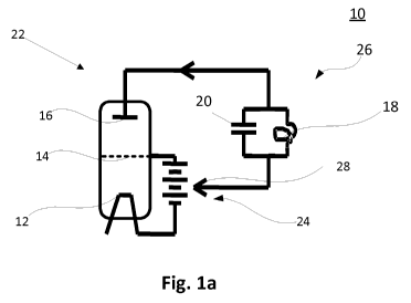
Fig. la shows a schematic view of a miniaturized device 10 for generating THz
radiation according to
the invention. The device 10 comprises a Dynatron tube 22, a battery 24, and
an oscillator 26.
The Dynatron tube, consists of a cold field emitter cathode 12, an
electrostatic extractor in form of an
electron transparent grid 14 positioned opposite to the field emitter cathode
12 and an anode 16. All the
components of the Dynatron tube are enclosed in an evacuated environment.
The anode 16 is coated with a material layer, which allows a strong emitting
of secondary electrons. The
transparent extractor grid 14 is formed of two metallic beams.
Furthermore the oscillator 26 is embodied in a circuit composed from an
inductance 18, a capacitor 20
and a metal wiring to connect the oscillator circuitry 26 to the voltage
connecting point 28 at the grid
voltage battery 24, supplying an alternating voltage to the anode 16. The
battery 24 supplies a high grid
voltage and a lower anode voltage.
Fig.lb shows the current (l_anode) / voltage (U_anode) characteristics of the
anode, which is obtained
due to the effect, that at a certain height of the anode voltage an increased
number of secondary elec-
trons is generated at the anode, which fly back to the higher grid potential
and generate a resulting
anode current, which can even become negative. The working potential point 30
is situated where the
anode current becomes zero. At this point emission current is equaled by the
secondary electrons
emitted from the anode.
Fig. lc the Dynatron oscillator, and the wiring of the components, which is to
be produced on an insu-
lating substrate using optical- or electron ¨beam lithography and a standard
lift-off process as a wiring
pattern, onto which by computer controlled EBID for the cathode the electron
emitter is constructed in
form of a hair pin, which can be heated by a heater current, and also
extractor rods and anode rods are
constructed using the computer controlled EBID technology. Aso an unheated
single rod EBID electron
emitter can be used.
Fig. 1c shows a possible layout for the device. Here the cathode 12 and the
extraction grid 14 are
shown as fabricated with electron beam induced deposition as rods of 200 nm
diameter and 1 pm in
length, both deposited on metal lines prefabricated by lithography and lift-
off technology on an insulating
substrate (not shown). Also the anode 16 is shown as a deposited rod structure
of e.g. 1 pm in height,
CA 02806448 2013-01-24
20
coated with a high SE emitting material. Furthermore the oscillator comprises
a parallel plate capacitor
20 and an inductance 18 of appropriate size, which can be just a line and
needs not to be a circular
loop.
The device 10 additionally comprises a potential divider voltage pickup 32
from a resistor, also fabri-
cated by EBID to set the voltage for the oscillator middle voltage point of
the battery 24.
It is anticipated that a total size of the miniaturized device is < 20 x 20
pm. This is much smaller than the
expected emitted wavelength of the THz-radiation;
Fig. 2 shows a schematic layout of the metallization pattern of the device 40
including the EBID emitter
42, extractor grid 44 and anode 46 of a miniaturized Dynatron tube combined
with a LC oscillator 47,
comprising an inductance 48 and a capacitor 50, which assembles to a Tera-
Hertz-Source with Free
Electron Beam. In this preferred embodiment of the invention the distance
between electron emitter 42
and extractor grid 44 of the tube is fabricated in a miniaturized way not
larger than 0.1*A/2 of the THz
radiation to be emitted. At the distance of 0.1 X up to X/2 to the extractor
grid 44, the anode 46 is
placed.The distance is limited by the time of flight of the released secondary
electrons and the oscillator
voltage swing.
The oscillator base voltage that is supplied by battery 52 is chosen in a
magnitude, that primary current
and resulting backward current have a balanced charge and therefore emit the
THz radiation in phase
and with equal amplitude. This Dynatron-THz radiation source needs only one
electron beam source 58,
but needs a larger footprint than the Dynatron tube itself due to the -
oscillator circuit. A primary electron
beam 54 ¨represent as full lines ¨ is emitted from this electron beam source.
A secondary electron
beam 56 ¨dashed lines ¨ is generated in the anode 46 by the second half wave
which is set to be a
secondary beam current that is twice the primary beam current.
The secondary beam current is emerging from the anode due to excitation by the
impact of the primary
electrons and enhanced by a special coating of the anode. Both electron beams
are free electron
beams and therefore emit a high amount of radiation.
Fig. 3 shows a possible wiring pattern layout for a Miniaturized Dynatron
Oscillator Tera-Hertz-Source
60 similar to that of Fig. 2, but with multiple parallel free electron beams
in one circuit with one vibration
oscillator supplying the anode voltage with THz frequency, emitted from
multiple cathode emitter tips 62,
CA 02806448 2013-01-24
21
each having an extractor 68 and the grid to anode 70 flight distance is
adapted to the flight time of
secondary electrons in the time of half a oscillation, required to emit the
half wavelength of the THZ
electromagnetic radiation by the primary beam in the first half wave and as
the voltage from the
oscillator circuit 66 generates by the resulting backward flying charge from
the high secondary electron
beam attracted by the extractor grid 68 in the second half wave. The IR
radiation is generates in a
smaller area than a wavelength, but can be selected and guided by a resonator
of V2 dimensions.
Increasing the number of beams in one plane raises the power of the emitted
electromagnetic radiation.
In this embodiment the multiple parallel free electron beams emitted from
multiple miniaturized EBID-
field emitter tips 62 and controlled by the multiple EBID extractor rods 64
one each for each field emitter
tip 62. The Anode 70 is also a larger number of EBID rods in parallel
fabricated with EBID with a mate-
rial with the appropriate SE-emission coefficient and characteristic for the
backward current having twice
the size of the primary current. As already shown in Fig. 3, the full lines
represent the primary electron
beam, the dashed lines represent the free beams in the second half wave, which
is set to a voltage
which generates a secondary electron beam current which is twice the primary
beam current.
Fig. 4 shows a schematic lateral view of a Miniaturized Dynatron Oscillator
Tera-Hertz-Source with one
free electron beam built within a cavity resonator 80. All the components of
the device are built on an
insulating substrate 88 with radiation reflecting base into the side walls of
the cavity resonator 80. The
cavity is encapsulated by a focusing lens 74. The focusing lens 74 is made
from silicon or other THz
transparent material shaped to focus the THz-radiation.
The distance between the extractor grid 82 and an anode 84 is 0.01 to 0.5 of a
wavelength of the THz
radiation. The base material 90 and the insulating substrate 88 is an Si02 ,
Diamond, or Boron nitride
insulator coating. The vacuum filled free space of the cavity resonator
structure 80 works like a
spectrometer in so far that the resonator dimensions select a stable
electromagnetic wavelength and
amplifies and sends this along its axis. Cavity resonators 80 are known in
microwave technology since
long as conductors for THz radiation energy. They need to have a good
conductivity in their walls and
are generally closed on 4 sides around their axis.
Figure 5 shows a schematic lateral view of a THz Emitter Cell 105 comprising
two Dynatron tubes 99 to
generate two Free Electron Beams built into a cavity resonator 94 with
conducting sidewalls on top and
bottom of a central base 100 with a hole 98 of the size of0.01 to 0.5 of a
wavelength and with the cavity
CA 02806448 2013-01-24
22
closed by radiation transmitting and focusing lenses 104 on each side. The two
identical Dynatron tubes
99 each comprise an electron source 96, extractor grid 97, and an anode 102.
The free electron beams emitted in synchrony on top and bottom of the base 100
from the electron
sources 96 to the anode 102 across a hole 98 in the base 100. The base 100 is
built from an insulating
material and fabricated into a cavity resonator. This preferred embodiment
delivers a doubled radiation
power compared to the single beam system.
Fig. 6 shows a schematic representation like Fig. 5 of a miniaturized Dynatron
Oscillator Tera-Hertz-
Source with Getter material. In this advantageous embodiment of the invention,
supplying the vacuum to
the miniaturized Dynatron Oscillator Tera-Hertz-Source is achieved due to a
pumping cell 92 hat is
attached to the miniaturized Dynatron Oscillator THz Source. The pumping cell
92 contains a vacuum
pump, like a miniaturized Orbitron pump , as tought by H. Koops Miniaturized
Orbitron Pump
DE000010241549B4 (not shown in this figure) in a cavity 110 where the cavity
110 is connected to the
THz resonator.
In difference to the embodiment in Fig. 5 one wall of the cavity resonator is
replaced by a pumping cell
wall 106 that is vacuum transparent, and designed as a good conducting THz
reflector, e.g. a tight metal
grid side wall with pitch << A THz radiation.
The base 100 that stretches from the cavity resonator 80 into the pumping cell
92 is coated with getter
material 108 on its bottom and top surface. This provides a chemical pumping
power by the composition
of the getter material and its activation by heating to absorb gas atoms and
chemically bind those in
solid deposits. In this way the gas volume is depleted from gas molecules, and
the cavity is pumped to a
high vacuum over very long times, e.g. years.
Fig. 7 shows a cross-section drawing of a miniaturized Dynatron Oscillator
Tera-Hertz-Source. The
miniaturized Dynatron Oscillator Tera-Hertz-Source has an attached pumping
cell 92 like Fig. 6. The
free flying electron beams in the THz-cavity resonator 94, 106 emit radiation
through lenses 104 and the
beam is directed with mirrors 112 and with a focusing lens 114 to form and
focus the beam.
Using the mirrors 112, the beams emitted through the lenses 104 in opposite
directions can be bundled
by the lens 114, which leads to a beam with doubled intensity.
CA 02806448 2013-01-24
23
Fig. 8 is a schematic side view of a Miniaturized Dynatron Oscillator Tera-
Hertz-Source with a blade
shaped an metal edge emitter 124 to emit free electron beams. The emitted
electron beams are focused
by an extractor cylinder lens structure 126 made from two metal blade shaped
electrodes having a slot
in between and through which the extracted cold field electron emitted
electron beam is focused to the
anode 132. Metal edge emitter 124, cylinder lens structure 126, and anode 132
form a Dynatron tube
130 that is built into a cavity resonator 134 closed with a transparent THz-
radiation focusing lens 128.
The grid 126 to anode 132 distance is 0.01 to 0.5 of a wavelength .The base
120 material and
resonator bottom 122 is e.g. an Si02 insulator coating the base 120. The
vibrating circuitry 136 is also
fabricated near the anode 132 which is also coated with or made from a
material with a high secondary
emission factor to generate the reverse flying net charge in the second half
wave, not shown. The
device furthermore comprises a highly conductive resonator side wall 134, and
a lens 128 made from
silicon or other THz transparent material shaped to focus the THz-radiation.
This preferred embodiment of a THz source uses a much higher primary current
than a single point field
emitter source due to the several nm in size the metal line surface protruding
crystal edges generated in
the metal deposition process, and has the advantage that it can be fabricated
with standard optical and
electron beam lithography and all MEMS fabrication compatible fabrication
process steps, and does not
need the expensive FEBIP Focused Electron Beam Induced Processing Technology.
The extension of
the cathode and focusing lens should be confined to <0.5, preferred < 0.1 of
the half wavelength of the
emitted radiation to generate a good dipole radiation emission characteristic.
Preferred materials for
edge emitter 124 are noble metals, and alloys having a characteristic crystal
size in the 10 nm regime
Fig. 9 shows a schematic of a miniaturized Dynatron Oscillator Tera-Hertz-
Source with two metal edge
emitters 124 where each emits free electron line beams that are extracted with
the help of an extractor
cylinder lenses 126. The free electron beams are emitted in synchrony on top
and bottom of a base 140
from the electron sources 124 to the anodes 132 across a hole 142 in the
insulating base 140, having a
vibration oscillator structure like on the top of the base also on the bottom
of the base built into a cavity
resonator 144 with two focusing lenses 128 for THz radiation on each side.
This preferred embodiment
delivers a doubled radiation power compared to the single beam system.
Preferred material of edge
emitters 124 are noble metals, and alloys having a characteristic crystalline
structure in the 10 to 100
nm regime.
This type of a miniaturized Dynatron Oscillator Tera-Hertz-Source may also be
combined with a vacuum
cell like shown in Fig. 6 or Fig. 7,
CA 02806448 2013-01-24
24
Fig.10 shows schematic top view of a tunable THz Dynatron Source 150 with two
wires 160 and current
flow driven NiTiNOL-stage for fine tuning by moving one wall 156 of the cavity
resonator and moving the
anode 158 with a lever 154.
The system is encapsulated with all surrounding walls of a frame 152 fixed to
a base plate 153. The
cavity is evacuated using Getter pumping with Getter material 162 placed in
the area of the NiTiNOL
stage setup.
There are NiTiNOL wires 160 for pulling right or left. The wire contracts up
to 5% if heated by current
flow. To achieve repeated contraction the wires are expanded by a spring 164
after contraction is suffi-
cient to reach a position of the lever 154. The wires act against a block 166
positioned unmovable rela-
tive to the frame 152 and base plate 153. The spring 164 is used to expand the
wire if no further con-
traction is needed. The two wires act on a lever 154. This pivots around an
axis 168. The lever-position
is stabilized by friction between the lever 154 and the base plate 153, both
having fine ground surfaces,
and the ax s 168 is plate spring loaded to press the lever 154 to the base
plate 153. The position of the
lever 154 can be monitored with high precision using e.g. strain gauges on a
beam, which is mounted
with one end on the base plate 153 and is bent by the lever motion.
An insulator plate 168 carrying the anode 158 is linked via a push and pull
rod 170 to the lever 154.
VVith pivoting the lever, the resonator wall 172 that is also bound to the
insulator plate 168 as well as the
anode 158 can be moved relative to the cathode assembly 174 and the frame 152.
The position of the
insulator plate 168 is adjusted due to wanted wavelength.
Two or more such engines can be employed to move the resonator wall in
perpendicular directions, and
also with one movement the anode.
Fig. 11 a shows a schematic circuitry view of a setup comprising a dynatron
tube 180 connected to two
free beam triodes 182, 184 to generate THz radiation.
According to this setup the dynatron tube 180 is used as a source for an
oscillating grid-voltage applied
to the grids 186, 188 of two separate provided vacuum triodes 182, 184 which
are overlaid to each other
to generate two free electron beams 190, 192 which are flying in opposite
direction and are switched by
the grid voltage which is for the second tube reversed in polarity by a
capacitor 194, which is placed in
CA 02806448 2013-01-24
25
the grid supply line of the second tube. This results in the effect that the
two in opposite direction flying
beams also fly having opposite phase to each other.
The cathode 200 of a first free beam tube 182 and the cathode 202 of a second
free beam tube 184
having opposite phase to the first tube 182 and opposite beam direction. To
emit the THz radiation in
synchronism and at the same location the tubes are fabricated on the same
substrate on top of each
other that is described in Fig. 1111
In between the tubes 182, 184 is a capacitor 194, which reverses the
controlling voltage of the grid 186,
188, which controls the electron emission current of the cathodes 200, 202.
Fig. 11b shows as a detailed side view of the two free beam triode tubes 182,
184 having opposite
phase and beam direction that are constructed in one plane. The triode tubes
182, 184 as described in
Fig. 11a each comprises a cathode 200, 202 and each a anode 204, 206.
Fig. 11c shows the mask layout for the metal line wiring pattern which is to
be the top view of the layout
of the THz DYNATRON oscillator tube 180 and two free beam triode tubes 182,
184 having opposite
phase and direction, which are controlled by the oscillator voltage as grid
voltage. The triode tubes 182,
184 are designed in an superimposed fashion to guarantee the same line of
radiation emission of the
two free beam triode tubes 182, 184, which emit electrons in an alternating in
phase linked fashion. The
anode 204 of the first free beam tube 182, and the anode 206 of the second
free beam tube 184 are
arranged in the same plane. The voltage supply for the anodes is not shown,
however, selecting a
voltage as high as electrically possible in the miniaturized design allows to
increase the emitted IR
radiation power. The phase shifting capacity 194 is responsible for the
backward beam and changes the
sign of the voltage for the backward beam. The oscillating current emits THz
radiation;
The triodes may be produced on an insulating substrate by optical or electron
beam lithography and
using lift-off- metallization, which is in parts used for the deposition of
the field electron cathode 200, 202
and the extractors grids 186, 188.
Fig. 11d shows the tube emission current versus time for the two tubes in one
graph.
Fig. 12 shows a further embodiment of the device, as a schematic circuit
layout for the three
components of a Miniaturized Dynatron Oscillator Tera-Hertz-Source with a
Dynatron Oscillator for THz
CA 02806448 2013-01-24
26
voltage oscillations. This voltage is amplified , if necessary with at least
one stage amplifier, which is
built with EBID as a micro triode to amplify the THz voltage signal, used to
control the extractors 186,
188 of two free beam electron sources which each send the beam into and across
a resonator 204,206.
The two powerful field emission micro triodes send their beam through a hole
in the resonator cavity
204,206, which serves as an anode with a hole to transmit the beam through the
resonator 204,206 as a
free flying electron beam. The beam impinges finally to the resonator wall,
since the extractor voltage at
the exit hole is negative at the end of the time of flight of the first beam,
since a signal reversal is built in
with the capacitor 194, to obtain an electron beam in the second half
oscillating voltage period, when the
first extractor 186 has a negative voltage.
One electron source is supplied with the amplified oscillator voltage to
control the emitted electron beam
in the first half of the oscillation with positive value with respect to the
cathode 200, a coupling capacitor
194 is used to reverse the signal, which then controls the extractor 186, 188
for the second electron
beam source to send the electrons into the resonator 204,206 in the second
half wave of the oscillating
voltage from the right side to generate the second half wave of the Hertz
dipole radiation. The amplifier
stage 208 can rise the extraction voltage for the electron beam sources 200,
202 to the working point for
high field emission current. The separate voltage supplied to the resonator
204, 206 as an anode
voltage rises the beam energy and therefore increases the radiation output of
the IR source up to 47 %
of the pulse beam power inside the resonator.
The amplified voltage which oscillates with the THz frequency as given by the
Dynatron 180 is therefore
fed to a THz radiation generator,
The amplifier stage 208, is fabricated like the Dynatron triode and the
electron emitter triodes by EBID
on prefabricated metal lines. The intermediate amplification is beneficial to
provide high extraction
voltages to obtain a high electron beam which in turn is a high charge pulse
which emits the THz-IR
Hertz Dipole radiation. The layout of such an one-stage or, as given here, a
two-stage amplifier is
designed according to state of the art radio signal amplifiers, but in
contrary to radio frequency
amplifying tubes, here THz signal amplifying miniaturized field emission
triodes are used. They cover a
footprint of the layout of < 10 pm x 10 pm.
Fig. 12 a shows a a schematic circuit layout for the three components of a
Miniaturized Dynatron
Oscillator Tera-Hertz-Source with a Dynatron oscillator for THz voltage
oscillations, built as a serial
resonator, with two triode electron sources 200, 202, which are controlled by
the oscillator voltage in
CA 02806448 2013-01-24
27
their emissions, and by the anode voltage of the resonator, in their energy.
The two triode beams 192 fly
through the tube in the bottom of the resonator 204,206 , where an aperture
212 connects the
electromagnetic radiation from the charge pulses into the resonator 204, 206,
where one forward and
one backward flying pulse excite one wavelength of the IR radiation.
The setting mentioned in Fig.12 a may be embedded in a housing analogue to
Fig. 5 to Fig. 9.
CA 02806448 2013-01-24
28
List of reference signs
10 miniaturized device
12 emitter cathode
14 grid
16 anode
18 inductance
20 capacitor
22 dynatron tube
24 battery
26 oscillator
28 voltage connecting point
30 working point
32 voltage pickup
40 device
42 EBID-emitter
44 extractor grid
46 anode
47 oscillator
48 inductivity
50 capacitor
52 battery
54 primary electron beam
56 second electron beam
58 beam source
60 Miniaturized Dynatron Oscillator Tera-Hertz-Source
62 emitter tips
CA 02806448 2013-01-24
29
64 extractor rods
66 oscillator circuit
68 extractor
70 anode
72 cathode
74 focusing lens
76 emitter tip
78 primary electron beam
80 cavity resonator
82 extractor grid
84 anode
86 cavity
88 insulating substrate
90 base material
92 pumping cell wall
94 cavity resonator
96 electron source
97 extractor grid
98 cavity
99 Dynatron tube
100 central base
102 anode
104 focusing lenses
105 THz Emitter Cell
106 pumping cell wall
108 getter material
110 cavity
112 mirror
114 focusing lens
120 base
122 insulating resonator bottom
124 metal edge emitter
126 cylinder lens structure
128 focusing lens
CA 02806448 2013-01-24
30
130 Dynatron tube
132 anode
134 cavity resonator
136 oscillator
140 base
142 hole
150 Dynatron Source
152 frame
153 base plate
154 lever
156 moving one wall
158 anode
160 wires
164 spring
166 block
168 axis
170 pull rod
172 resonator wall
174 cathode assembly
180 dynatron tube
182 free beam triodes
184 free beam triode
186 extractor grid
188 extractor grid
190 free electron beam
192 free electron beam
194 capacitor
196 oscillator
200 cathode
202 cathode
204 anode
206 anode
208 stage amplifier
210 aperture