Note: Descriptions are shown in the official language in which they were submitted.
CA 02806543 2014-09-09
TITLE:
A NOVEL EMBEDDED 3D STRESS AND TEMPERATURE SENSOR
UTILIZING SILICON DOPING MANIPULATION
INVENTORS:
HOSSAM MOHAMED HAMDY GHARIB and WALIED AHMED
MOHAMED MOUSSA
TECHNICAL FIELD:
[0001] The present disclosure is related to the field of piezoresistive stress
sensors, in
particular, piezoresistive stress sensors that are capable of extracting all
six stress
components with temperature compensation.
BACKGROUND:
[0002] The measurement of stresses and strains is essential for the
inspection,
monitoring and testing of structural integrity. A commonly used technique for
stress and
strain monitoring is the use of metallic strain gauges. These gauges utilize
the strain-
electrical resistance coupling to evaluate the in-plane strains when they are
surface
mounted to a structure, which is useful in structural health monitoring of
machinery,
bridges and bio-implants. However, if an evaluation of the out-of-plane normal
and
shear stress/strain components is required, metallic strain gauges offer
limited
advantage.
[0003] An alternative technique to overcome this limitation would be to use
the silicon
piezoresistive stress/strain gauges, which can offer higher sensitivity
compared to
metallic strain gauges, ability to measure out-of-plane stress/strain
components and
provide in situ real-time non-destructive stress measurements. The majority of
the
developed piezoresistive stress/strain sensors use elements that sense in-
plane stress
and/or strain components for applications in pressure sensors [1],
microcantilevers [2],
or strain gauges [3]. However, fewer efforts are spent towards the utilization
of the
(E6687007 DOC: 2)
CA 02806543 2014-09-09
2
unique properties of crystalline silicon to develop a piezoresistive three-
dimensional
(3D) stress sensor that measures the six stress components. These types of 3D
stress
sensors can be valuable in applications where the sensor and the monitored
structure
are of the same material, such as in cases where an electronic chip is used to
measure
the stresses due to packaging and thermal loads [4, 5]. Also, a 3D stress
sensor can be
used in applications where the sensor is embedded within a host material to
monitor the
stresses and strains at the sensor/host material interface. In the latter
case, a coupling
scheme can be used to link the stresses and strains in the sensor to those in
the host
material [6, 7].
[0004] The piezoresistive effect in silicon was observed through experimental
testing by
Smith [8] and Paul et al. [9] in the 1950s. Since then, a lot of research work
has been
conducted to study the piezoresistive effect and its relation to other
parameters like
electrical resistivity, electrical mobility, impurity concentration and
temperature. The
change in resistance of a piezoresistive filament can be related to the
applied stress
and/or temperature through the piezoresistive coefficients and temperature
coefficient of
resistance (TCR), respectively. Piezoresistive coefficients were studied
experimentally
by Tufte et al. [10, 11], Kerr et al. [12], Morin et al. [13], and Richter et
al. [14].
Analytical modeling of the piezoresistive coefficients and their relation to
temperature
and impurity concentration can be attributed to Kanda et al. who provided
graphical
representation of the piezoresistive coefficients with crystallographic
orientation [15, 16].
Also, they presented analytical and experimental studies for the first and
second order
piezoresistive coefficients in both p-type and n-type silicon [17-21]. Other
theoretical
modeling of the piezoresistive effect was introduced by Kozlovsky et al. [22],
Toriyama
(E6687007.DOC; 2}
CA 02806543 2014-09-09
3
et al. [23] and Richter et al. [24]. Temperature coefficient of resistance in
silicon was
studied by Bullis et al. [25] and Norton et al. [26]. A study on the effect of
doping
concentration on the first and second order temperature coefficient of
resistance was
conducted by Boukabache et al. using the models for majority carriers mobility
in silicon
[27].
[0005] The first piezoresistive stress-sensing rosette capable of extracting
four of the six
stress components was designed by Miura et al. [28]. This sensing rosette is
made up
of two p-type and two n-type sensing elements on (001) silicon wafer plane and
extracts
the three in-plane stress components and out-of-plane normal stress component.
The
first comprehensive presentation of the theory of piezoresistive stress-
sensing rosettes
was given by Bittle et al. [29] and later re-constructed by Suhling et al. to
include the
effect of temperature on the resistance change equations and study the
application of
stress-sensing rosettes to electronic packaging [5]. The aforementioned two
studies
introduced the first piezoresistive dual-polarity stress-sensing rosette
fabricated on
(111) silicon using both n- and p-type sensing elements that can extract the
six stress
components. The extracted stresses were partially temperature-compensated,
where
only four stresses are temperature-compensated, namely the three shear
stresses and
the difference of the in-plane normal stresses. Their inability to extract all
stresses with
temperature-compensation is due to the limitation in the number of independent
equations that hinders the ability to eliminate the effect of temperature on
the change in
electrical resistance of the sensing elements. Other studies for the
development of 3D
piezoresistive stress sensors for electronic packaging applications include
the works of
Schwizer et al. [4], Lwo et al. [30], and Mian et al. [31].
{E6687007 DOC; 2}
CA 02806543 2014-09-09
4
[0006] To the inventors' knowledge, for all developed 3D stress sensors
publicly
available, none are capable of extracting all six stress components with
temperature
compensation. It is, therefore, desirable to provide 3D stress sensors that
overcome
the shortcomings of the prior art.
SUMMARY:
[0007] A novel approach is provided to building an embedded micro dual sensor
that
can monitor stresses in 3 dimensions ("3D") and temperature. The approach can
use
only n-type or a combination of n- and p-type silicon doped piezoresistive
sensing
elements to extract the six stress components and temperature.
[0008] In some embodiments, the approach can be based on generating a new set
of
independent linear equations through the variation in doping concentration of
the
sensing elements to develop a fully temperature-compensated stress-sensing
rosette.
[0009] In some embodiments, the rosette can comprise an all n-type (single-
polarity) 3D
stress-sensing rosette instead of the combined p- and n-type (dual-polarity).
In some
embodiments, a single-polarity approach can reduce the complexity associated
with the
microfabrication of the dual-polarity rosette and can enable further
miniaturization of the
size of the rosette footprint.
[0010] Broadly stated, in some embodiments, stress sensor is provided,
comprising: a
semiconductor substrate; a plurality of piezoresistive resistors disposed on
the
substrate, the resistors spaced-apart on the substrate in a rosette formation,
the
resistors operatively connected together to form a circuit network wherein the
resistance
of each resistor can be measured; and the plurality of piezoresistive
resistors
comprising a first group of resistors, a second group of resistors and a third
group of
(E6687007.DOC; 2)
CA 02806543 2014-09-09
resistors wherein the three groups are configured to measure six temperature-
compensated stress components in the substrate when the sensor is under stress
or
strain.
[0011] Broadly stated, in some embodiments, a strain gauge is provided
comprising a
sensor, the sensor comprising: a semiconductor substrate; a plurality of
piezoresistive
resistors disposed on the substrate, the resistors spaced-apart on the
substrate in a
rosette formation, the resistors operatively connected together to form a
circuit network
wherein the resistance of each resistor can be measured; and the plurality of
piezoresistive resistors comprising a first group of resistors, a second group
of resistors
and a third group of resistors wherein the three groups are configured to
measure six
temperature-compensated stress components in the substrate when the sensor is
under
stress or strain.
[0012] Broadly stated, in some embodiments, a method is provided for measuring
the
strain on an electronic chip comprising a semiconductor substrate, the method
comprising the steps of: fabricating the electronic chip with a plurality of
piezoresistive
resistors disposed on the substrate, the resistors spaced-apart on the
substrate in a
rosette formation, the resistors operatively connected together to form a
circuit network
wherein the resistance of each resistor can be measured, the plurality of
piezoresistive
resistors comprising a first group of resistors, a second group of resistors
and a third
group of resistors wherein the three groups are configured to measure six
temperature-
compensated stress components in the substrate when the sensor is under stress
or
strain; subjecting the electronic chip to a mechanical or thermal load;
measuring the
{E6687007 DOC; 2}
CA 02806543 2014-09-09
6
resistance of the resistors; and determining the six temperature compensated
stress
components of the substrate from the resistance measurements.
[0013] Broadly stated, in some embodiments, a method is provided for measuring
strain
or stress on a structural member, the method comprising the steps of: placing
a strain
gauge on or within the structural member, the strain gauge comprising a
sensor, the
sensor further comprising: a semiconductor substrate, a plurality of
piezoresistive
resistors disposed on the substrate, the resistors spaced-apart on the
substrate in a
rosette formation, the resistors operatively connected together to form a
circuit network
wherein the resistance of each resistor can be measured, and the plurality of
piezoresistive resistors comprising a first group of resistors, a second group
of resistors
and a third group of resistors wherein the three groups are configured to
measure six
temperature-compensated stress components in the substrate when the sensor is
under
stress or strain; subjecting the structural member to a mechanical or thermal
load;
measuring the resistance of the resistors; and determining the six temperature
compensated stress components of the substrate from the resistance
measurements.
BRIEF DESCRIPTION OF THE DRAWINGS:
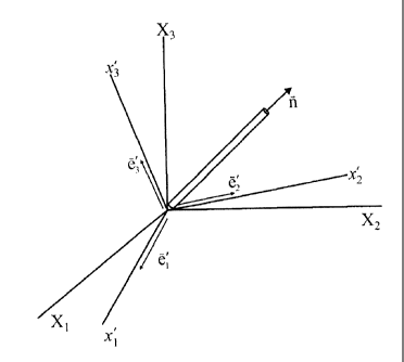
[0014] Figure 1 is a three-dimensional graph depicting a filamentary silicon
conductor.
[0015] Figure 2 is a two-dimensional graph depicting a silicon wafer with
filament
orientation.
[0016] Figure 3 is a two-dimensional graph depicting a ten-element
piezoresistive
sensor.
[0017] Figure 4 is a contour plot depicting the effect of doping concentration
of groups a
and b on P11 for an npp rosette.
{E6687007.DOC; 2}
CA 02806543 2014-09-09
7
[0018] Figure 5 is a contour plot depicting the effect of doping concentration
of groups a
and b on 1D21 for an npp rosette.
[0019] Figure 6 is a contour plot depicting the effect of doping concentration
of groups a
and b on IDil for an nnn rosette.
[0020] Figure 7 is a contour plot depicting the effect of doping concentration
of groups a
and b on 1D21 for an nnn rosette.
[0021] Figure 8 is a two-dimensional graph depicting the effect of doping on B
in p-Si.
[0022] Figure 9 is a two-dimensional graph depicting the effect of doping on B
in n-Si.
[0023] Figure 10 is a two-dimensional graph depicting the effect of doping on
TCR in n-
Si and p-Si.
[0024] Figure 11 is a microphotograph of a fabricated nnn rosette.
[0025] Figure 12 is a perspective view depicting a four-point bending loading
fixture.
[0026] Figure 13 is a photograph depicting the probing of piezoresistors under
uniaxial
loading with a physical implementation of the fixture of Figure 12.
[0027] Figure 14 is a two-dimensional graph depicting typical stress
sensitivity from four-
point bending measurements for RD.
[0028] Figure 15 is a two-dimensional graph depicting typical stress
sensitivity from four-
point bending measurements for R90.
[0029] Figure 16 is a two-dimensional graph depicting typical temperature
sensitivity
measurements.
DETAILED DESCRIPTION OF EMBODIMENTS:
Theoretical Background
{E6687007.DOC;
CA 02806543 2014-09-09
8
[00301A piezoresistive sensing rosette developed over crystalline silicon
depends on
the orientation of the sensing elements with respect to the crystallographic
coordinates
of the silicon crystal structure. An arbitrary oriented piezoresistive
filament with respect
to the silicon crystallographic axes is shown in Fig. 1. The unprimed
coordinates
represent the principal crystallographic directions of silicon, i.e. X1 =
[100], X2 = [010],
and X3 = [001], while the primed axes represent an arbitrary rotated
coordinate system
with respect to the principal crystallographic directions.
[0031] The change in electrical resistance of a piezoresistive filament due to
an applied
stress and temperature along the primed axes is given by [5]:
AR R(o-,T)- R(0,0)
R(0,0)
=(7rficiJP)/ 2 (Jr;flu'fi)m' +.(g;ficr:,)n4
(1)
4-2(gcr:g)1v
+[a,T + azT2 + .
Where,
R(o-, T) = resistor value with applied stress and temperature change
R(0, 0) = reference resistor value without applied stress and temperature
change
= off-axis temperature dependent piezoresistive coefficients with y, =
1,2,...6
= stress in the primed coordinate system, = 1,2,..,6
a2, = = = = first and higher order temperature coefficients of resistance
(TCR)
T=71-Tref= difference between the current measurement temperature (T) and
reference
temperature (Tref)
i',m',n' = direction cosines of the filament orientation with respect to
the x, 4, and 4 axes
[0032] The orientation defined by the primed axes for a set of piezoresistive
filaments
forming a rosette determines the number of stress components that can be
extracted.
For example, a rosette oriented over the (001) plane can be used to measure
the in-
plane stress components and the out-of-plane normal component. On the other
hand, a
rosette oriented over the (111) plane can extract the six stress components.
Moreover,
a (001) rosette can extract two temperature-compensated stress components,
while the
{E6687007 DOC; 2}
CA 02806543 2014-09-09
9
(111) rosette can extract four temperature-compensated stress components by
eliminating the component (a7) in equation (1) [32]. Therefore, to develop a
3D stress
sensing rosette over the (111) wafer plane, equation (1) is reformulated into:
AR
¨ =(B, cos' + B, sin2 0)(7;1 +(B2 cos' 0+ B, sin' 0)o-22
+ B,o-'3,+2,5(B2¨ B3)(cos2 ¨ sin2 0)0:23
+ 2-sh(B, ¨ B,)sin 20-;, + (B,¨ B2)sin 20a,2 + aT
(2)
[0033] In which only the first order temperature coefficient of resistance (a)
is
considered, q5 is the angle defining the orientation of a piezoresistive
filament over the
(111) plane as shown in Fig. 2 and a (i=1,2,3) is a function of the
crystallographic
piezoresistive coefficients as follows:
+ + 71- + 77-
B, ¨ ___ 4 B, ¨ ___ 4,
2 6
and B, = ir" 21;12 ir" (3)
Sensing Rosette Theory (Current Approach)
Basic Concept
[0034] The 3D stress sensing rosette presented by Suhling et al. is made up of
eight
sensing elements; four n-type and four p-type [5]. Suhling et al. reported in
this study
that a (111) sensing rosette fabricated from identically doped sensing
elements (single-
polarity) can only extract three stress components. On the other hand, a (111)
dual-
polarity rosette can extract the six stress components because it provides
enough
linearly independent responses from the sensing elements.
[0035] In fact, the dual-polarity rosette provides two sets of independent
piezoresistive
coefficients (7c) and temperature coefficients of resistance (a), which
generate linearly
independent equations to extract the six stresses with partial temperature-
{E6687007.DOC; 2}
CA 02806543 2014-09-09
compensation. Therefore, if it is possible to have two groups of sensing
elements (not
necessarily dual-polarity) with independent TC and a, the partially
temperature-
compensated six stress components can be extracted. Moreover, if a third group
with
different Ir and a is added, fully temperature-compensated stress components
can be
extracted.
[0036] Solution for Stresses
[0037] In some embodiments, a rosette can be made up of ten sensing elements
developed over the (111) wafer plane as shown in Fig. 3 and can be divided
into three
groups (a, b, and c), where each group has linearly independent TC and a.
Eight of these
elements, forming groups a and b, can be used to solve for the four
temperature-
compensated stresses similar to the dual-polarity rosette of Suhling et al.
[5]. The extra
two sensing elements forming the third group c can be used to solve for the
remaining
temperature-compensated stress components. Application of equation (2) to the
rosette
gives ten equations describing the resistance change with the applied stress
and
temperature:
[A-1--?,)= Ba;, + l3o-;, + Bc7;, +150'2' ¨ BDo-3+ ceT
(AR, ).( )cr _F
B, + B;, (A + B:)(7,22 13,3,(7;,
R2 2 2
+ 2 NE(B: ¨ B:)o-:, + (B," ¨ 13:)o-:2 + a'T
AR' j= B o-'I + 22 + B"o-33 ' ¨ f3)cr;,+
\ R3 2 I I 3
(AR, +(Br ,
R, 2 I 2 22
-2-5(,57 - 13)o-;3 - (B," - B' )a2 + a'T
[`6?' j= +131;o-L + Ba, + 2,5(Bi; )aL + ceT
Rs
( AR61
+ B110.1, I +(A' + BI;)aL B,;(7;3
R6 2 2
+ 2-12-(Bi; -/3)a, +(B," -/3)a, + abT
(AR7j= 131;o-;, + crL + 13:cr3-2,5(B ¨ B.1;)ctL + cebT
R7
{E6687007.DOC; 2}
CA 02806543 2014-09-09
11
AR8, õ.(B,b+Bno.1,1+f + Bnc42+
2 ) 2 )
¨ 2[(B; ¨ B;)o-3 ¨ BI;)a;2+ abT
(A-A)= Ba +14.7;2+ B;o-;, +2-5(B; ¨ B;)o-;,+
Rs
AR')= + B;cr;,+ B;o-;3-2-4-(B;. ¨ 13;)o-;3 + (4)
R,0
[0038] Superscripts a, b, and c can indicate the different groups of elements.
The
evaluation of the stresses and temperature can be carried out by the
subtraction and
addition of equations (4) to give:
Equations for the evaluation of ( 'i-62)and
AR AR
_ 3 -
R, R, (Bi ¨ B) 4-5(B; ¨14) a;2 (5)
AR5_ AR7 (BbB) 0`; ¨ crZ3
R5 R, -
Equations for the evaluation of o- and cs-L
AR2 _ AR4
R2 R4 - 4./ 2 ¨ B;) 2(k ¨13) [c431 (6)
AR6_ AR8 (B; ¨ 2(B; ¨ 81;) Cr12
R6 Rs _ -
Equations for the evaluation of (
,411-111-1- 0-212) a313 and T
AR, 4. AR3
R, + 2B; 2ce- (0-:1 + 22)
A 7 = (B,b+B;) 2B; 2ot' a;2 (7)
R5 R7
AR9 ARio , + 2a` T
R9 R,õ
[0039] The expressions in (5)-(7) can be inverted to solve for the stresses
and
temperature in terms of the measured resistance changes as shown in (8)-(10),
where
01 can describe the determinants of the coefficients in (5) and (6), and D2
can describe
the determinant of the coefficients in (7).
(E6687007.DOC, 2}
CA 02806543 2014-09-09
12
[0040] Dual- and Single-Polarity Rosettes
[0041] The solution of (8) requires non-zero D1 and D2, which means that each
of the
three sets of equations (5)-(7) must be linearly independent. This is achieved
in two
ways; using a dual-polarity rosette or a single-polarity rosette designated as
npp and
nnn respectively as shown in Table 1.
TABLE 1
= SELECTED DOPING TYPES OF EACH ROSETTE
Rosette Group a Group b Group c
npp n-type p-type (1) p-type (2)
nnn n-type (1) n-type (2) n-type (3)
(E6687007.DOC, 2)
CA 02806543 2014-09-09
13
[0042] The npp rosette can comprise n-type group a elements, and p-type groups
b and
c elements but with a different doping concentration designated as (1) and (2)
in Table
1. This selection of sensing elements can offer different and independent
coefficients in
(5)-(7), thus independency of the equations.
D,,[(B;crb + R,) R5
¨ B;a )(T: + A 71+(B:a' ¨ B;'ceb)[._t A., 4
,B, Bo(AR:_A::) R5 R_(õ
_,)(As A RR.:)]
2D, _k R
ii;[(BabAIR?3)+Al??: ARR:)+01;a R5 R,0 +ARR:j1
__L
2D, R,1 R, 6:77)]
0-,= -[((4b-Eg)a'¨(B+B)ab)(A k+A--1-1+((4+B)AY¨(Br-EB7)ce)(65+ A 7)4-(6T +BDce
BDal[AR9 AR1
2D2 A Rs Rs Rs R9 A.
ci.; (B__B)r, AR3) (Br_Bo(AR, AR7)]
R, R, ) 4J R, R,
1[¨(B r AR4) (Br ¨ ( AR, AR, 11
3 4,5 R2 R4 ) 4,fi R6 R8 )
a; ¨ R2 A AR4) (13; ¨ BO*R8
A)1
D, 2 R2 R4) 2 R6 Ra )]
T = 1 [((4` + B )BI; +B'),&; + 3)+((B BDB; + 4)BOH 115 + A
7)+((B +B)B' = BDBO(A 9 +A1A (8)
24 2 A Rs Rs Rs R9 Rio
Where,
(9)
(10)
{E6687007.DOC; 2}
CA 02806543 2014-09-09
14
[0043] The nnn rosette can have n-type sensing elements for all three groups,
but with
different doping concentration designated as (1), (2) and (3) in Table 1. This
selection
of sensing elements can be attributed to the unique piezoresistive properties
of n-Si
compared to p-Si. In p-Si, the three crystallographic piezoresistive
coefficients 1T121
and 1T44) vary with the same factor upon variation of doping concentration and
temperature [10, 15, 16]. This can hinder the possibility of developing an all
p-type
rosette. Therefore, in some embodiments, p-type sensing elements have to be
combined with n-type sensing elements to solve (8).
[0044] In n-Si, the values of the on-axis piezoresistive coefficients 1ri and
7-ci 2 vary with
the same factor in response to the change in doping concentration and
temperature
[15]. However, the shear piezoresistive coefficient 71-44 in n-Si can behave
in a different
manner than the other two coefficients. Tufte et al. [10, 11] reported that
upon change
in impurity concentration, the absolute value of 1T44 shows no change until an
impurity
concentration of around 1020 cm-3, then it starts showing a logarithmic
increase of its
absolute value compared to the decreasing 7-/-1 and 7r12. Kanda et al.
provided an
analytical model to describe this behavior of 1T44 with impurity
concentration. The
electron transfer theory can be used to describe correctly the behavior of
7c11 and 7c12 in
n-Si. However, when used to describe the behavior of 1T44 it suggested a zero
value for
the coefficient [18, 19]. Therefore, they proposed using the theory of
effective mass
change to describe the behavior of 1T44 and it was found to satisfy the
experimental
results given by Tufte et al. [11]. Also, Nakamura et al. analytically modeled
the n-Si
piezoresistive behavior and discovered that 744 hardly depends on
concentration over
the range from 1x10¹⁸ to 1x1020 cm-3 [33]. Such behavior is paramount in the
design of
{E6687007 DOC; 2}
CA 02806543 2014-09-09
the single-polarity n-type sensing rosette because it helps create groups a,
b, and c with
independent B and a coefficients, thus providing independent equations (5)-
(7).
Temperature Effects
[0045] Piezoresistors can be sensitive to temperature variation, which changes
the
mobility and number of carriers. These temperature variations can affect the
values of
(1) the resistance of the sensing element by the temperature function
[f(T)=ai T+a1 T2+...], (2) the piezoresistive coefficients (n), and (3) the
temperature
coefficient of resistance, TCR (a). The reduction of these unwanted variations
can
impact on the calculated stresses is addressed in this section. The
temperature
function f(7) in piezoresistive sensors is usually eliminated by the addition
of an
unstressed resistor and use it to subtract the temperature effect from the
stress
sensitivity equations. However, this approach would be difficult to implement
in
applications that do not have an unstressed region in close proximity to the
sensing
rosette like in cases of embedded sensors. In some embodiments, two resistors
of the
same doping level and type can be adopted to subtract the temperature effects.
This
method is adopted in equations (5) and (6), therefore, the stresses extracted
from (5)
and (6) can be independent of temperature effect on resistance. On the other
hand, f(T)
can be included in (7) in order to be evaluated and compensate for its effect
in the
remaining stress equations, i.e. c:, , , and 0-;, .
[0046] Experimental studies on the effect of temperature on n- and doping
concentrations were conducted by Tufte et al. [10] for a large range of
concentrations
and temperatures and compiled from the literature by Cho et al. [34]. It is
noticeable
that at high doping concentrations, the effect of temperature on n- is
decreased, which is
(E6687007 DOC; 2}
CA 02806543 2014-09-09
16
verified analytically by Kanda et al. [15]. Similarly, at high doping levels
the TCR value
remains constant with temperature variations, thus giving a linear f(T)
function. Cho et
al. studied the effect of temperature on the TCR value on heavily doped n-type
resistors
from -180 C to 130 C. They concluded that a first order TCR is adequate to
model the
f(7) function at high doping concentrations [35]. A similar conclusion is
reached by
Olszacki et al. for p-type silicon, where the quadratic terms in f(T) were
found to
approach zero at high doping levels [36].
[0047] Based on the previous behavior of 7T and TCR, the doping level of the
proposed
rosettes can be selected to be at high concentrations to minimize the effect
of
temperature on both ir and TCR. In some embodiments, calibration of 7T and TCR
can
be carried out over the operating temperature range of the rosette, which can
enhance
the accuracy of the extracted stresses.
Analytical Verification
[0048] In some embodiments, the analytical verification of the presented
approach can
be based on evaluating D1 and D2 at different doping concentrations for the
three
groups of sensing elements (a, b, and c) in order to study the behavior of D1
and D2 with
concentration and their range of non-zero values. The analysis can be based on
the
analytical values of 7/- for n- and p-Si given by Kanda [15], the experimental
values of /44
for n-Si given by Tufte et al. [11], and the experimental values of a for n-
and p-Si given
by Bullis et al. [25] for uniformly doped piezoresistors. The analysis can be
carried out
over a range of doping concentrations from 1x10¹⁸ to 1x102 cm-3 to avoid the
constant
behavior of the piezoresistive coefficients at low doping concentrations which
will affect
the linear independency of (5)-(7) and to minimize the effect of temperature
on it and a.
{E6687007 DOC: 2}
CA 02806543 2014-09-09
17
[0049] D1 and D2 Coefficients
[0050] The evaluation of D1 and D2 at different concentrations for the npp and
nnn
rosettes are shown in Fig. 4 to Fig. 7, where Na and Nb are the doping
concentrations of
groups a and b respectively. The doping concentration of group c for both
rosettes is
set at 5x1018 cm-3.
[0051] In the case of npp rosette, D1 has a maximum at the low doping
concentration
(1x1018 cm-3) for both groups a and b of the analyzed range as shown in Fig.
4. On the
other hand, D2 is shown to have a maximum at (Na, Nb) = (1x1018 cm-3, 1x10¹⁸
cm-3) and
(1x1018 cm-3, 1x1029 cm-3) as shown in Fig. 5. Regarding a zero determinant,
IN is
always positive because groups a and b have independent r and a. Contrarily,
D2
reaches a zero value at two concentrations. The first is when group b has the
same
doping concentration as group c, i.e. 5x1018 cm-3 and the second when group b
has the
same TCR value of group c at 1x1019 cm-3.
[0052] For nnn rosette, D1 shown in Fig. 6 has a maximum at the boundaries of
the
range, i.e. at (Na, Nb) = (1x10¹⁸ CM-3, 1x102 cm-3) and (1x1029 cm-3, 1x10¹⁸
cm-3) and
reaches zero when both groups a and b have the same doping concentration. The
zero
value occurs when groups a and b have the same coefficients, thus giving
dependent
equations (5)-(6). On the other hand, as shown in Fig. 7, D2 has two peaks at
(Na, Nb) =
(1x102 cm-3, 2x1019 cm-3) and (2x1019 cm-3, 1x1029 cm-3) and reaches zero
when: (1)
both groups a and b have the same concentration and (2) any of groups a or b
has the
same concentration as group c (i.e. 5x1018 cm-3). These many zero valleys
found in
Fig. 7 requires more caution in the selection of the appropriate
concentrations for
groups a, b, and c. It is important to note that if a different concentration
for group c is
{E6687007 DOC; 2}
CA 02806543 2014-09-09
18
selected, the contour plots of D2 can be different, but a non-zero solution
can still be
achieved.
[0053] It is clear that finding non-zero D1 and D2 is possible for both npp
and nnn
rosettes by selecting different doping concentration for each group. The
relatively large
range of non-zero D1 and D2 on the contour plots in Fig. 4 to Fig. 7 eases the
process of
doping by allowing larger tolerance on the concentration of the doped sensing
elements.
This is important in cases where the accuracy and reproducibility of the
doping process
is low as in the case of diffusion as compared to ion implantation.
B and TCR Coefficients
[0054] The selection of the doping concentrations of groups a, b and c can be
based on
finding non-zero D1 and D2. However, another condition is still important to
analyze,
which is maximizing B and a. These coefficients can determine the sensitivity
and
output of the sensing elements for each of the seven components (six stress
components and temperature) as given by (4). It is important to maximize the
values of
these coefficients to maximize the sensitivity and to avoid running into
measurement
errors during calibration. However, maximizing these coefficients means
lowering the
doping concentration, which maximizes the variation of the piezoresistive
coefficients
and TCR due to temperature changes. Therefore, in some embodiments, the doping
concentration can be selected such that B and a can be maximized, while
minimizing
the effect of temperature on the coefficients.
[0055] The B coefficients for p-Si, shown in Fig. 8, show a mutual decrease
with the
increase in doping concentration due to the common factor relating the
piezoresistive
coefficients with doping concentration. On the other hand, the B coefficients
for n-Si in
{E6687007 DOC, 2}
CA 02806543 2014-09-09
19
Fig. 9 decrease with doping concentration except for 83, which shows an almost
constant behavior with doping concentration. This constant trend of 83 is due
to its
primary dependence on 744, which as noted earlier is independent of impurity
concentration up to 1x102 cm-3. The TCR (a) curves for p- and n-Si with
doping
concentration is shown in Fig. 10 as extracted from the work of Bullis et al.
[25], where a
for n-Si is zero at around 1.5x10¹⁸ and 7x1018 cm-3. Therefore, it is
important to avoid
those values in order to avoid measurement errors during calibration.
[0056] The present analysis is based on assuming uniform doping concentration
of the
sensing elements.
For actual sensor rosette fabricated using diffusion or ion
implantation, the sensing elements can have non-uniform distribution of
dopants across
the thickness of the chip which follows either a Gaussian or complementary
error
function profile. This non-uniform doping of the sensing elements were not
considered
in the presented analysis due to the unavailability of enough experimental or
analytical
data for non-uniformly doped piezoresistors. However, according to Kerr et
al., the
surface dopant concentration could be used as an average effective
concentration to
model the piezoresistivity of diffused layers. [12].
Experimental Verification
[0057] A preliminary experimental analysis to verify the feasibility of the
proposed
approach for the single polarity rosette (nnn) was carried out. The analysis
verifies the
feasibility of our approach of finding non-zero values of D1 and D2 for three
groups of n-
Si sensing elements at different concentrations. Test chips with the nnn
sensing
rosettes are microfabricated on (111) silicon wafers at the advanced MEMS/NEMS
design laboratory and the NanoFab at the University of Alberta (U of A). A
{E6687007 DOC, 2}
CA 02806543 2014-09-09
microphotograph of the fabricated ten-element nnn rosette is shown in Fig. 11
with the
corresponding number for each resistor. Phosphorus diffusion with solid
sources is
used to create the three groups of serpentine-shaped resistors. The three
concentrations were 2x10²⁰, 1.2x10² and 7x1019 cm-3 for groups a, b and c,
respectively and as shown in Fig. 3 and as labelled in Fig. 11, which were
characterized
using secondary ion mass spectrometry (SIMS) in the ACSES lab at the U of A.
This
range of concentrations is slightly different than the previous analytical
study due to the
limitation with the used diffusion sources in reaching lower concentrations.
Calibration
[0058] The evaluation of 01 and D2 for the fabricated rosette requires
calibration of the B
coefficients. The B1 and B2 coefficients are calibrated by applying uniaxial
loading on
the sensing elements oriented at 0 and 90 with respect to the 1-direction
awl (refer to
Fig. 3). This gives the following normalized resistance change equations:
[AiLl= B, a;,
Ro (eff)
( 1 1 )
(AR-\= B a;,
R90
[0059] where, Bi(eff) and B2(eft) are effective values of the B coefficients
which include the
effect of the transverse sensitivity of the serpentine-shaped resistors. In
order to
eliminate this error and extract the fundamental values of the piezoresistive
coefficients
of silicon, the following correction relationship proposed by Cho et al. is
used [37]:
B, =713,
2r-1
A = rB,),ff) + (7- 1) ( ( 1 2)
2y-1
{E6687007.DOC; 2}
CA 02806543 2014-09-09
21
[0060] where r is the ratio of the axial section to the sum of axial and
transverse
sections of the resistor, as shown in Fig. 11, such that r = Nax/( Nax+ N
1 and N. and
trans,
Ntrans are the number of squares in the axial and transverse sections of the
resistor.
[0061] A four-point bending (4PB) fixture 10 was used to generate a uniaxial
stress on a
rectangular strip or beam 12 cut from the fabricated wafer as shown in Fig.
12, which
contains a row of test chips. The four point loading develops a state of
uniform bending
stress between supports 14 at the middle section of the beam, which develops a
state
of uniaxial stress with a maximum value at the upper and lower surfaces of
beam 12
given by [38]:
3F(L- D)
cr:i=
Wt, (13)
[0062] where, F = applied force, L = distance between the two dead weights 16,
D =
distance between the middle supports 14, w = width of rectangular strip or
beam 12,
and t = thickness of rectangular strip 12. This equation is accurate if beam
12 is not
significantly deformed due to the applied load, F, and the dimensions w and t
are small
compared to L and D.
[0063] The applied 0-;, stress generated between the two middle supports
ranged from 0
to 82 MPa; and the measurement of the piezoresistors under loading is done
using
probes 18, as shown in Figs. 12 and 13. Sample stress sensitivity data from
the 4PB
measurements for the Ro and Rgo resistors are shown in Fig. 14 and Fig. 15,
respectively.
[0064] The remaining piezoresistive coefficient B3 requires an application of
either a
well-controlled out-of-plane shear stress (0-;, or 03 ) or hydrostatic
pressure. However, as
{E6687007 DOC; 2}
CA 02806543 2014-09-09
22
a preliminary study, B3 is evaluated based on the known relationship of the
hydrostatic
pressure coefficient (71-p) with 81, 82, and B3, where rcp = -(81+82+83) as
noted by
Suhling et al. [5]. Experimental values for irp in n-Si is given by Tufte et
al. over a
concentration range from 1x10¹⁵ to 2x10²⁰ cre and presented in Table 2 for
each group
of our resistors [11]. Once B3 is evaluated, the fundamental piezoresistive
coefficients
are calculated from (3).
[0065] The temperature coefficient of resistance (a) is calibrated by using a
hot plate to
measure the change in resistance with temperature increase. The temperature is
varied
from 23 C to 60 C. Sample temperature sensitivity measurements are shown in
Fig. 16,
where T represents the temperature change from 23 C. The measured values of
Bi(eft),
B2(eff), and a as well as the calculated values of B and n- for the three
groups are shown
in Table 2 along with their corresponding D1 and D2 values. These values are
averaged
over 10 specimens with their standard deviations noted between parentheses in
the
table.
[0066] The temperature coefficient of resistance (a) is calibrated by using a
hot plate to
measure the change in resistance with temperature increase. The temperature is
varied
from 23 C to 60 C. Sample temperature sensitivity measurements are shown in
Fig. 16,
where T represents the temperature change from 23 C. The measured values of
81(e),
82(eff), and a as well as the calculated values of B and n- for the three
groups are shown
in Table 2 along with their corresponding D1 and D2 values. These values are
averaged
over 10 specimens with their standard deviations noted between parentheses in
the
table.
{E6687007.DOC; 2}
CA 02 80 65 43 2 014-0 9-0 9
23
TABLE 2
EXPERIMENTAL VALUES FOR B, a, AND D
Group a
N, cm-3 2x10² 1.2x10² 7x10¹⁹
gp, TPa-1 [11] 27 26 25
-72.0 -76.5 -116.3
Bi(eff), TPa-1
(13.5) (10.4) (13.6)
64.7 69.0 108.1
82off), TPa-1
(11.1) (10.4) (4.5)
81, TPa-1 -75.2 -80.8 -124.5
B2, TPa'l 67.8 73.3 116.4
B3, TPa-1 34.4 33.5 33.1
, TPa-1 -175.5 -200.1 -374.3
/r12, TPa-/ 101.2 113.1 199.7
.744, TPa-1 -76.1 -74.5 -74.4
1425.5 1208.6 1055.6
a, ppm/ C
(189) (162) (184)
ID11, TPa-2 538.3
1D21, x103 TPa-2 C-1 3.1
D Coefficients
[0067] The results in Table 2 indicate that the present set of piezoresistors
have non-
zero Di and D2 values, which proves the validity and feasibility of the
proposed
approach. An important observation from the experimental results is that
although the
concentration levels of groups a, b and c are close, a solution is still
possible for
obtaining a non-zero Di and D2. A larger difference between the concentrations
of the
three groups is expected to provide higher D values as indicated by the
analytical study
and illustrated in Fig. 6 and Fig. 7.
{E6687007.D0C; 2)
CA 02806543 2014-09-09
24
Fundamental piezoresistive coefficients
[0068] A decreasing trend of the fundamental piezoresistive coefficients kill
and 11T121 is
shown in Table 2 to develop in the range from group c (low concentration) to
group a
(higher concentration) with no major change in 744. This aligns with the
previous
experimental results reported by Tufte et al. [11] and the analytical
calculations by
Kanda et al. [18, 19] and Nakamura et al. [33]. Consequently, the B
coefficients
presented in Table 2 demonstrate similar trends to those presented in Fig. 9,
where B1
and B2 show a monotonic decrease from group c to group a, while B3 shows
almost no
change. This behavior of 7Z" and B coefficients confirms the fundamental
concept upon
which the presented approach for npp and nnn rosettes is based, i.e. the
independence
of 744 with impurity concentration. Thus, these results prove the feasibility
to develop the
nnn (single-polarity) and npp (dual-polarity) rosettes.
TCR (a)
[0069] The values of TCR in Table 2 is seen to increase from 1055.6 ppm/ C at
low
concentration to 1425.5 ppm/ C at higher concentration. This trend agrees with
the
experimental results of Bullis et al. shown in Fig. 10 [25] and the analytical
models of
Norton et al. [26]. Moreover, the good linear fit of the TCR-resistance data
proves that
the assumption of neglecting the second order TCR is valid over the studied
doping
concentration and temperature ranges.
[00701 In some embodiments, a new approach is provided for developing a
piezoresistive three-dimensional stress sensing rosette that can extract the
six
temperature-compensated stress components using either dual- or single-
polarity
sensing elements.
In some embodiments, temperature-compensated stress
{E6687007 DOC; 2}
CA 02806543 2014-09-09
components can be extracted by generating a new set of independent equations.
In
some embodiments, a technique is provided that can comprise three groups of
sensing
elements with independent piezoresistive coefficients (a) and temperature
coefficient of
resistance (TCR) and can further use the unique behavior of ram in n-Si to
construct
dual- and single-polarity rosettes.
[0071] In some embodiments, the piezoresistive resistor sensor as described
herein can
be used as micro stress sensors for a variety of applications. In some
embodiments,
the sensor can be used to monitor the thermal and mechanical loads affecting
an
electronic circuit or chip during its packaging or operation. The sensor can
act as a
device for monitoring the structural characteristics of an electronic chip. In
other
embodiments, the sensor can also be used to monitor the operation of the chip
under
thermal and mechanical loading to provide data that can be used to design
electronic
circuits and chips that can withstand greater thermal and mechanical loads and
stresses.
[0072] In other embodiments, the sensor can be incorporated into a strain or
stress
gauge or device for use in monitoring the strain or stress on or within a
structural
member. For the purposes of this specification, the strain gauge or device can
be
placed on a surface of the structural member or embedded within the structural
member
as obvious to those skilled in the art. In addition, a structural member can
include a
structural element of a machine, a vehicle, a building structure, an
electronic device, a
bio-implant, a neural or spinal cord probe or electrode, an electro-mechanical
apparatus
and any other structural element of an object as well known to those skilled
in the art.
{E6687007.DOC; 2}
CA 02806543 2014-09-09
26
[0073] Although a few embodiments have been shown and described, it will be
appreciated by those skilled in the art that various changes and modifications
might be
made without departing from the scope of the invention. The terms and
expressions
used in the preceding specification have been used herein as terms of
description and
not of limitation, and there is no intention in the use of such terms and
expressions of
excluding equivalents of the features shown and described or portions thereof,
it being
recognized that the invention is defined and limited only by the claims that
follow.
REFERENCES
[1] D. Benfield, E. Lou, and W. Moussa, "Development of a MEMS-based sensor
array
to characterise in situ loads during scoliosis correction surgery," Computer
Methods
in Biomechanics and Biomedical Engineering, vol. 11, no. 4, pp. 335-350, Aug,
2008.
[2] F. Goericke, J. C. Lee, and W. P. King, "Microcantilever hotplates with
temperature-
compensated piezoresistive strain sensors," Sensors and Actuators a-Physical,
vol.
143, no. 2, pp. 181-190, May 16, 2008.
[3] A. A. S. Mohammed, W. A. Moussa, and E. Lou, "Optimization of geometric
characteristics to improve sensing performance of MEMS piezoresistive strain
sensors," Journal of Micromechanics and Microengineering, vol. 20, no. 1, pp. -
,
Jan, 2010.
[4] J. Schwizer, M. Mayer, O. Brand et al., "Force sensors for microelectronic
packaging
applications," Microtechnology and MEMS, Springer, 2005, pp. viii, 178 p.
[5] J. C. Suhling, and R. C. Jaeger, "Silicon piezoresistive stress sensors
and their
application in electronic packaging," Sensors Journal, IEEE, vol. 1, no. 1,
pp. 14-30,
2001.
[6] F. Alfaro, L. Weiss, P. Campbell et al., "Design of a multi-axis
implantable MEMS
sensor for intraosseous bone stress monitoring," Journal of Micromechanics and
Microengineering, vol. 19, no. 8, pp. -, Aug, 2009.
[7] C. Hautamaki, S. Zurn, S. C. Mantell et al., "Experimental evaluation of
MEMS strain
sensors embedded in composites," Microelectromechanical Systems, Journal of,
vol. 8, no. 3, pp. 272-279, 1999.
[8] C. S. Smith, "Piezoresistance Effect in Germanium and Silicon," Physical
Review,
{E6687007 DOC; 2}
CA 02806543 2014-09-09
27
vol. 94, no. 1, pp. 42-49, 1954.
[9] W. Paul, and G. L. Pearson, "Pressure Dependence of the Resistivity of
Silicon,"
Physical Review, vol. 98, no. 6, pp. 1755-1757, 1955.
[10] O. N. Tufte, and E. L. Stelzer, "Piezoresistive Properties of Silicon
Diffused Layers,"
Journal of Applied Physics, vol. 34, no. 2, pp. 313-318, 1963.
[11] O. N. Tufte, and E. L. Stelzer, "Piezoresistive Properties of Heavily
Doped n-Type
Silicon," Physical Review, vol. 133, no. 6A, pp. A1705, 1964.
[12] D. R. Kerr, and A. G. Milnes, "Piezoresistance of Duffused Layers in
Cubic
Semiconductors," Joumal of Applied Physics, vol. 34, no. 4, pp. 727-&, 1963.
[13] F. J. Morin, T. H. Geballe, and C. Herring, "Temperature Dependence of
the
Piezoresistance of High-Purity Silicon and Germanium," Physical Review, vol.
105,
no. 2, pp. 525-539, 1957.
[14] J. Richter, O. Hansen, A. N. Larsen et al., "Piezoresistance of silicon
and strained
Si0.9Ge0.1," Sensors and Actuators a-Physical, vol. 123-24, pp. 388-396, Sep
23,
2005.
[15] Y. Kanda, "A graphical representation of the piezoresistance coefficients
in silicon,"
Electron Devices, IEEE Transactions on, vol. 29, no. 1, pp. 64-70, 1982.
[16] Y. Kanda, "Piezoresistance effect of silicon," Sensors and Actuators, A:
Physical,
vol. 28, no. 2, pp. 83-91, 1991.
[17] Y. Kanda, and K. Matsuda, "Piezoresistance effect in p-type silicon,"
Physics of
Semiconductors, Pts A and B, vol. 772, pp. 79-80 1594, 2005.
[18] Y. Kanda, and K. Matsuda, "Piezoresistance Effect of n-type Silicon;
Temperature
and Concentration Dependencies, Stress Dependent Effective Masses," AIP
Conference Proceedings, vol. 893, no. 1, pp. 173-174, 2007.
[19] Y. Kanda, and K. Suzuki, "Origin of the shear piezoresistance coefficient
pi 44 of n-
type silicon," Physical Review B, vol. 43, no. 8, pp. 6754, 1991.
[20] K. Matsuda, Y. Kanda, and K. Suzuki, "2nd-Order Piezoresistance
Coefficients of
N-Type Silicon," Japanese Journal of Applied Physics Part 2-Letters, vol. 28,
no. 10,
pp. L1676-L1677, Oct, 1989.
[21] K. Matsuda, Y. Kanda, K. Yamamura et al., "2nd-Order Piezoresistance
Coefficients of P-Type Silicon," Japanese Journal of Applied Physics Part 2-
Letters
& Express Letters, vol. 29, no. 11, pp. L1941-L1942, Nov, 1990.
{E6687007 DOC; 2}
CA 02806543 2014-09-09
28
[22] S. I. Kozlovskiy, and I. I. Boiko, "First-order piezoresistance
coefficients in silicon
crystals," Sensors and Actuators a-Physical, vol. 118, no. 1, pp. 33-43, Jan
31,
2005.
[23] T. Toriyama, and S. Sugiyama, "Analysis of piezoresistance in p-type
silicon for
mechanical sensors," Journal of Microelectromechanical Systems, vol. 11, no.
5, pp.
598-604, Oct, 2002.
[24] J. Richter, J. Pedersen, M. Brandbyge et al., "Piezoresistance in p-type
silicon
revisited," Journal of Applied Physics, vol. 104, no. 2, pp. -, Jul 15, 2008.
[25] W. M. Bullis, F. H. Brewer, C. D. Kolstad et al., "Temperature
coefficient of
resistivity of silicon and germanium near room temperature," Solid-State
Electronics,
vol. 11, no. 7, pp. 639-646, 1968.
[26] P. Norton, and J. Brandt, "Temperature-Coefficient of Resistance for P-
Type and N-
Type Silicon," Solid-State Electronics, vol. 21, no. 7, pp. 969-974, 1978.
[27] A. Boukabache, and R. Pons, "Doping effects on thermal behaviour of
silicon
resistor," Electronics Letters, vol. 38, no. 7, pp. 342-343, 2002.
[28] H. Miura, A. Nishimura, S. Kawai et al., "Structural Effect of lc Plastic
Package on
Residual-Stress in Silicon Chips," 40th Electronic Components and Technology
Conference, Vols 1 and 2, pp. 316-321, 1125, 1990.
[29] D. A. Bittle, J. C. Suhling, R. E. Beaty et aL, "Piezoresistive stress
sensors for
structural analysis of electronic packages," Journal of Electronic Packaging,
vol.
113, no. 3, pp. 203-215, 1991.
[30] B. J. Lwo, J. S. Su, and H. Chung, "In Situ Chip Stress Extractions for
LFBGA
Packages Through Piezoresistive Sensors," Journal of Electronic Packaging,
vol.
131, no. 3, pp. -, Sep, 2009.
[31] A. Mian, J. C. Suhling, and R. C. Jaeger, "The van der Pauw stress
sensor," IEEE
Sensors Journal, vol. 6, no. 2, pp. 340-356, Apr, 2006.
[32] R. A. Cordes, J. C. Suhling, Y. L. Kang et al., "Optimal temperature
compensated
piezoresistive stress sensor rosettes," American Society of Mechanical
Engineers,
EEP. pp. 109-116.
[33] K. Nakamura, Y. Isom, T. Toriyama et al., "Simulation of piezoresistivity
in n-type
single-crystal silicon on the basis of the first-principles band structure,"
Physical
Review B, vol. 80, no. 4, pp. -, Jul, 2009.
{E6687007 DOC, 2}
CA 02806543 2014-09-09
29
[34] C. H. Cho, R. C. Jaeger, and J. C. Suhling, "Characterization of the
temperature
dependence of the piezoresistive coefficients of silicon from-150 degrees C
to+125
degrees C," IEEE Sensors Journal, vol. 8, no. 7-8, pp. 1455-1468, Jul-Aug,
2008.
[35] C. H. Cho, R. C. Jaeger, J. C. Suhling et a/., "Characterization of the
temperature
dependence of the pressure coefficients of n- and p-type silicon using
hydrostatic
testing," IEEE Sensors Journal, vol. 8, no. 3-4, pp. 392-400, Mar-Apr, 2008.
[36] M. Olszacki, C. Maj, M. Al Bahri et al., "Experimental verification of
temperature
coefficients of resistance for uniformly doped P-type resistors in SOI,"
Journal of
Micromechanics and Microengineering, vol. 20, no. 6, pp. -, Jun, 2010.
[37] C. H. Cho, R. C. Jaeger, and J. C. Suhling, "The Effect of the Transverse
Sensitivity
on Measurement of the Piezoresistive Coefficients of Silicon," Japanese
Journal of
Applied Physics, vol. 47, no. 5, pp. 3647-3656, May, 2008.
[38] R. E. Beaty, R. C. Jaeger, J. C. Suhling et al., "Evaluation of
Piezoresistive
Coefficient Variation in Silicon Stress Sensors Using a 4-Point Bending Test
Fixture," leee Transactions on Components Hybrids and Manufacturing
Technology,
vol. 15, no. 5, pp. 904-914, Oct, 1992.
(E6687007 DOC; 2}