Note: Descriptions are shown in the official language in which they were submitted.
CA 02806935 2013-01-29
=
1
METHOD FOR SYNTHESISING A MATERIAL, IN PARTICULAR
DIAMOND, BY CHEMICAL VAPOUR DEPOSITION, AND A DEVICE
FOR APPLYING THE METHOD
The present invention concerns a method for synthesising a
material, in particular diamond, by chemical vapour deposition (CVD),
according to which a plasma is created in a vacuum chamber in the
vicinity of a substrate arranged to carry the material to be synthesised,
and according to which a substance carrying carbon, in particular CH4 or
C2H2, and H2, are introduced into the chamber in order to produce in the
chamber a gas comprising substances carrying reactive-carbon atoms in
the form of unsaturated molecules or radicals from which the synthesis of
said material will be performed.
Such a method is known from the patent US 4 859 490.
According to the known method a vacuum chamber is used, which is
maintained at a pressure of between 40 and 400 Torr and in which the
substrate is situated. The plasma is created by means of an electrical
potential applied between a filament and a grille, said grille being situated
between the filament and the substrate. The filament is heated to a
temperature of at least 1600 C and a carbon-carrying gas and H2 are
introduced into the chamber to enable diamond to be synthesised from
carbon by chemical vapour deposition.
One disadvantage of the known method is that the rate of
deposition of the solid material to be synthesised is low, around 1 pm per
hour, which means that the procedure, even if it procures synthetic
diamond of good quality, is not very profitable from the economic point of
view.
The aim of the invention is to produce a method for
synthesising a material by chemical vapour deposition, said method
making it possible to obtain a higher deposition rate than that of the
known method while having good quality of the material.
CA 02806935 2016-07-04
,
2
For this purpose a method according to one aspect of the invention is for
synthesising a material by chemical vapour deposition (CVD), according to
which a
plasma is created in a vacuum chamber in the vicinity of a substrate arranged
to
carry the material to be synthesised, and according to which a substance
carrying
carbon and H2 is introduced into the chamber in order to produce in the
chamber a
gas comprising substances carrying reactive carbon atoms in the form of
unsaturated molecules or radicals from which the synthesis of said material
will be
performed, characterised in that the electromagnetic absorption and inelastic
diffusion spectra of the material to be synthesised are used to take from the
spectra
the absorption frequencies that contribute to the reactions that lead to the
formation
of the material to be synthesised, and in that energetic rays are produced in
the
form of photon beams carrying quantities of energy determined by each of the
frequencies corresponding to said absorption and inelastic diffusion
frequencies,
said photon beam being injected into the plasma where, for energy states of
the
solid material, an absorption of these photons having the energy corresponding
to
these energy states is effected by the substances carrying said reactive
carbon
atoms.
Preferably, infrared rays are used as energetic rays for
effecting a coupling between the energy states of the unsaturated
molecules or radicals and the energy states of the photons of the
CA 02806935 2013-01-29
3
material. These infrared rays cover a wide range of frequencies present
in the spectrum of the material to be synthesised. A first preferential
embodiment of a method according to the invention is characterised in
that the material to be synthesised comprises a crystallographic lattice
that determines a set of facies, for example an octahedron, or a
dodecahedron in the case of diamond, represented by two sets of
directional vectors, the first indicating the directions normal to the main
reticular planes, with a higher atomic density determining the possible
facies of said material, the second consisting of the wave vectors allowed
for propagation of phonons according to the crystallographic structure of
the material, said photon beam being oriented and injected in directions
indicated by said two sets of directional vectors. In this embodiment the
method then consists of injecting photon beams having the energies of
the phonon modes w that are oriented according to corresponding wave
vectors K, lying in the Brillouin zone, which are taken from the dispersion
curves of said material, for example at the critical points and at the high-
symmetry points, including the centre of the zone normally denoted F.
These two sets of directions, relating to the respective meshes of the
direct lattice and the reciprocal lattice, in the end provide the directions
chosen for said photon beam. By taking account of these two sets of
vectors when the photon beam is injected, the probability of interaction
between the photons and the phonons is increased and this thus helps to
increase the rate of deposition of the material to be synthesised.
A second preferential embodiment of a method according to
the invention is characterised in that a beam of UVC rays is injected into
the plasma. The injection of a UVC beam in particular increases the
density of the plasma and thus stimulates the synthesis of the solid
matter.
A third preferential embodiment of a method according to the
invention is characterised in that the plasma is produced by creating an
electrical field in the vacuum chamber, said electrical field being created
CA 02806935 2016-07-04
4
by means of first and second electrical potentials, said first electrical
potential is
created in a first zone offset in the direction of the height with respect to
the
substrate and the second electrical potential is created in a second zone
situated in
the direct vicinity of the substrate, the first and second zones being
adjacent to
each other, said first and second potentials having a gradient directed
towards the
substrate, wherein the slope of the first potential is higher than that of the
second
potential. This makes it possible to better concentrate the substances
carrying
unsaturated molecules or in the form of radicals all around the substrate and
thus to
increase the probability of synthesising the material.
The invention also concerns a method for forming a semiconductor of type
Si¨Ge by chemical vapour deposition, characterised in that the deposition is
carried
out in a chamber and in that it comprises:
a chemical vapour deposition of silicon on a substrate at a temperature of
between 500 C. to 600 C. in the presence of hydrogen and having the chamber
maintained at a pressure situated between 0.01 and 1000 mbar, said deposition
being carried out by injecting into the chamber a photon beam corresponding to
the
frequency of the phonon due to the Si¨Si bond until the deposited layer of
silicon
has a thickness of at least 3 nm;
stabilisation of the temperature of the substrate at a first temperature
situated between 400 C. to 550 C.;
a chemical vapour deposition of germanium on the layer of Si at a
temperature of between 400 C. to 550 C. until a layer Ge is obtained at a
predetermined thickness with injection into the chamber first of a photon beam
corresponding to the frequency of the phonon due to the Si¨Ge bond and
secondly
another photon beam corresponding to the frequency of the phonon due to the
Ge¨
Ge bond;
incrementation of the temperature of the chemical vapour deposition to a
value situated between 750 C. and 850 C. in the presence of hydrogen;
CA 02806935 2016-07-04
4a
maintaining the injection of a photon beam corresponding to a frequency of
the phonon due to the Ge¨Ge bond until a predetermined thickness of layer is
obtained.
Another aspect of the invention concerns a device synthesising a material by
chemical vapour deposition (CVD), the material to be synthesised having a
crystallography with a set of possible faces, represented by a set of
directional
vectors where each vector indicates a direction normal to a given face of said
material, said device comprising a substrate arranged to carry the solid
material to
be synthesised and a vacuum chamber comprising a plasma generator arranged to
produce a plasma in the chamber in the vicinity of the substrate, said chamber
comprising an entry arranged to introduce into the chamber a substance
carrying
carbon, said chamber being arranged to produce therein, from the carbon-
carrying
substance and H2, a gas comprising radicals or molecules in unsaturated form
from
which the synthesis of said material will be effected, characterised in that
the device
comprises a photon beam generator mounted on the chamber and arranged to
produce energetic rays, in particular infrared rays and/or X, UV and visible
rays in
the form of a photon beam carrying quantities of energy determined by each of
the
frequencies corresponding to an absorption frequency taken from an
electromagnetic absorption and inelastic diffusion spectrum of the solid
material to
be synthesised and which produces a reaction that leads to the formation of
the
solid material to be synthesised, said photon beam generator being mounted on
the
chamber so that said beam produced can be injected into the chamber at an
angle
that corresponds both to the given directional vectors of said solid material
and to
the wave vector of the Brillouin zone associated with the energy of the photon
mode including the mode at the zone centre, determining the energy contained
in
the photon beam, said photon beam generator being mounted on the chamber in
order to be able to inject the photon beam into the plasma and, for energetic
states
of the solid material, caused by said substance carrying reactive carbon
atoms, an
CA 02806935 2016-07-04
4b
absorption of these photons having the energy corresponding to these phonic
states.
The invention will now be described in more detail with the help of the
drawings, which illustrate an example embodiment of a device according to the
invention. In the drawings:
figures la, b and c illustrate schematically the device according to the
invention;
figures 2 and 3 show emitters for producing the photon beam;
figure 4 illustrates an emitter for producing UVC;
figure 5 illustrates the method according to the invention as it occurs in the
device;
figures 6 to 8 show steps of the method;
figure 9 shows an absorption spectrum for diamond obtained by CVD;
figure 10 shows an example embodiment of a system for focusing the
plasma;
figure 11 shows first and second potentials; and
figure 12 illustrates the first Brillouin zone of the mesh of a material such
as
diamond.
In the drawings the same reference has been attributed to the same
elements or to a similar element.
CA 02806935 2013-01-29
, .
Figures la, b and c illustrate schematically an example
embodiment of a device according to the invention. Figure la shows the
structure of the device while figure lb shows the arrangement in space of
the elements of the device. The device 1 is arranged for applying a
5 method for
synthesising a material by hot filament chemical vapour
deposition (HFCVD). It will however be clear that the device illustrated
also allows any other method for synthesising a material by chemical
vapour deposition (CVD) and that the invention is not limited to the
HFCVD process but applies to any CVD process.
The device 1 illustrated in figures lb and c comprises a
vacuum chamber 2, which is preferably brought to a pressure of 10-3 Torr
before starting the synthesis process. The chamber is put under vacuum
in a known fashion, for example by means of a pump. In the chamber is
a substrate carrier 3, for example formed by a plate, arranged so as to
carry the material 17 to be synthesised. This material may be any
substance compatible for effecting the deposition, such as for example
diamond, W, WCCo, WCNi, silica, etc.
The substrate carrier is preferably connected to a first AC
voltage source 16 for reasons that will be described subsequently.
Where applicable, the substrate carrier is also connected to a DC source
16'. The substrate carrier 3 is preferably mounted on a cooling plate 18
serving to regulate the temperature of the substrate. For this purpose, an
entry 19A and exit 19B for cooling liquid are connected to this cooling
plate 18.
Above the substrate is a grille 4 and above the grille a filament
5. The filament is preferably mounted between two collimators 5A that
serve to focus the electrical field for better collimation of the plasma. The
collimators provide better distribution of the temperature, as well as of the
plasma in the deposition region. It should also be noted that the
invention is not limited to the position of the grille and filament as
illustrated in figures 1a and b, and that these positions may be reversed.
CA 02806935 2013-01-29
, .
6
The grille 4 is connected to a second voltage source 6 and the
filament 5 to a third voltage source 7. The second and third voltage
sources are DC voltage sources. The grille may when necessary also be
connected to a fourth AC voltage source (not included in the drawing).
The filament is also connected to a fifth voltage source 8 that is an AC
voltage source. The first, second and third voltage sources serve to vary
the electrical potential between the substrate, grille and filament, while
the fifth voltage source 8 serves for heating the filament. By varying the
electrical potential between the substrate, grille and filament, it is
possible to vary the electrical field in the chamber and thus control the
plasma that will be produced in the chamber. The voltage applied to the
filament and grille may vary between 0.1 and 400 volts according to the
material to be synthesised. The grille serves essentially to regulate the
flow of the chemical substances carrying unsaturated molecules or
radicals present in the chamber, while the filament serves to activate the
gas.
The device according to the invention also comprises a
system 9 for focusing the plasma placed at the periphery of the substrate
and arranged to improve the distribution of the temperature and plasma
in the region where the synthesis of the solid material will take place and
where the deposition is effected. Figure 10 illustrates an example of
such a system 9 for focusing the plasma. The plasma-focusing system is
for example formed by a ring 50 placed around the substrate and offset
towards the top of the chamber with respect to the substrate, The
focusing system 9 may also be formed by a set of metal wires bent
substantially in the form of an inverted U and placed around the
substrate. The plasma-focusing system is supplied by a sixth voltage
source 10, which supplies a direct current. The ring form for focusing the
plasma in relation to the filament is preferably implemented by two
semicircles placed on either side of the substrate carrier. The plasma-
focusing system 9 is preferably placed so as to be inclined towards the
CA 02806935 2013-01-29
7
substrate carrier in order better to focus the plasma towards the
substrate.
The device according to the invention also comprises photon-
beam generators 11-1 to 5 disposed above the chamber and arranged to
produce energetic rays, in particular infrared rays (IR), in the form of
photon beams. The number of photon-beam generators is determined
by the crystallography of the substance and is therefore is not limited to
the one set out in figures la and b. It is also possible, as in the
embodiment illustrated in figure lc, that there may be only one photon-
beam generator. This or these generators serve to produce energetic
rays the frequency of which is determined by the spectral density function
tp(w, K) of the material to be synthesised, where w represents the
frequency and K the wave vector, which is polarised or not in a plane, as
will be described below. Finally, the device is provided with a generator
12-1, 12-2 and 12-3 (the latter not being visible in the drawing)
generating beams of UVC rays. The latter generators are preferably
arranged in a circle, with in each case an angle of 120 between them for
reasons of symmetry.
It should be noted that, for reasons of clarity, only the
embodiment of the photon-beam generators arranged to produce
infrared rays will be described. However, the invention is not limited to
this embodiment and other energetic rays of the electromagnetic
spectrum that interact with the material may be used (X-rays, UV,
visible).
Since a plasma must be produced inside the chamber 2, the
device according to the invention also comprises an entry connected to a
supply source 13 for introducing into the chamber a carbon-carrying
substance, in particular in the form of a carbon-carrying gas, and
hydrogen (H2). The substance that is introduced is of course related to
the material to be synthesised. The source is connected to the chamber
by means of a flow control valve 14 arranged to regulate the flow rate of
CA 02806935 2013-01-29
8
the gas injected into the chamber. For forming diamond, the carbon-
carrying substance is introduced into the chamber in order to produce
therein a gas comprising substances carrying reactive carbon atoms in
the form of unsaturated molecules or radicals from which the synthesis of
the material will be effected. The carbon-carrying gas is for example
methane (CH4) or acetylene (C2H2). This synthesis reaction is known
per se and is for example described in the article by J E Butler, Y A
Mankelevich, A Cheesman, Jie Ma and M N R Ashfold entitled
"Understanding the chemical vapour deposition of diamond : recent
progress", which appeared in Journal of Physics Condensed Matter 21,
2009. Where necessary the gas may be preheated by means of heating
before entering the chamber. A gas-pumping unit 27 is connected to
the chamber in order to pump the gas and balance the pressure of gas
prevailing inside the chamber. For
forming a material other than
15 diamond,
the substance necessary for forming said material is introduced
into the chamber in order to produce therein a gas comprising
substances carrying base atoms of the reactive material in the form of
unsaturated molecules or radicals from which the synthesis of the
material will be effected.
The deposition zone is situated in the vicinity of the substrate.
It is in the deposition zone that the synthesis reaction takes place and it
is for this reason that, in the deposition zone, the temperature distribution
and the distribution of the chemical species to be activated must be very
homogeneous.
The method according to the invention is based on the
physical phenomenon of resonance during the selective excitation and
the coupling of the specific quantum states of the active chemical
species and the specific quantum states of the material to be
synthesised. This material to be synthesised may be either a solid
material, a liquid or even a gas. The objective of the invention is to
increase the efficiency of the synthesis method by allowing selective
CA 02806935 2013-01-29
. ,
9
transitions at the quantum state level. The method according to the
invention assists the probability of the formation by synthesis of a
material by imposing some of the specific quantum states, which
correspond to the effective or apparent absorption spectrum of this
material during the reaction steps and which lead to the formation of the
material.
The method according to the invention also promotes the
probability of the formation of a chemical species by imposing certain
specific quantum transitions corresponding to the material to be
synthesised. Finally, the method promotes the probability of formation of
a chemical species by imposing certain specific quantum states of the
chemical species to be synthesised on the reaction steps during the
formation corresponding to said chemical species.
In the method according to the invention, energies (EDAst),
which may act at various moments in the reaction, or during the entire
reaction, are introduced into the chamber. Thus there are:
- EDst; which is a dissociation energy the function of which is to
rupture some of the chemical bonds present in the substance and to form
selectively, in particular by resonance, starting substances or transient
substances that should then lead to the material to be synthesised. The
dissociation energy is for example produced by UVC rays.
- EAst: which is a structuring energy, forming, aggregating or
configuring the structure to be formed: its function is to fix the structure
of
the substance to be formed or synthesised.
The spectral density function FI.J(w,K] of the material to be
synthesised is composed of a sum of functions of the state spectral
densities
LP(w, K) = LPE(w, K) + Wv(w, K) + 1PR(w, K) + LPT(w, K)
where L-PE represents the electron state spectral density function, Lliv the
vibrational or phonic state spectral density function, 1PR the rotational
state spectral density function and IPT the translation state spectral
CA 02806935 2013-01-29
density function. Fuller details on this state spectral density function for
an example of diamond corresponding to the vibrational states are
described in the article by Claude Klein, Thomas Hartnett and Clifford
Robinson, entitled "Critical-point phonon frequencies of diamond", which
5 appeared in Physical Review B, Vol 45, N 22 of 1 June 1992. In
particular, for diamond, the global state spectral density function is
described by the sum of the spectral density functions of the electron
(WE(w,K)) and vibrational (L-Pv(w,K)) state spectral density functions.
When the material is formed by a liquid, the rotational states must be
10 taken into account and, for a gas, the translation states must be taken
into account.
The method according to the invention has recourse to this
state spectral density function or failing this to the effective or apparent
electromagnetic spectrum of absorption of the material to be
synthesised, see, for the example of diamond, the absorption spectrum
set out in figure 9 of the article by Klein et al. These electromagnetic
absorption spectra are spectra intrinsic to the material, or activated by
default. These electromagnetic absorption spectra are also inelastic
diffusion spectra of photons or neutrons of the material to be
synthesised. The absorption frequencies (f,) that characterise the
material to be synthesised and thus contribute to the reactions that lead
to the formation of the material to be synthesised are taken from the
electromagnetic absorption spectrum.
Thus, for example still referring to the article by Klein et al, the
17 1<i<17 energy levels set out in table II are taken, corresponding to the
two-photon spectrum (and (or) table I of the same article corresponding
to the one-photon spectrum). By means of these energy levels and the
absorption frequencies that correspond thereto, a photon beam carrying
a quantity of energy E, = hf, where h is equal to Planck's constant, will be
formed for each (i) of these frequencies f,. In this way, in the example of
diamond, seventeen photons beams are obtained, each having a well
CA 02806935 2013-01-29
11
determined quantity of energy E,. Naturally the number of frequencies
depends on the solid material to be synthesised. The choice of i=17 is
related to the example of the article by Klein et al, but in no way limits the
invention.
Naturally all the frequencies of the spectrum of the material to
be synthesised set out in figure 9 of said article could be taken.
However, in practice, it suffices to take the most representative ones and
those necessary for determining the material. Thus the values set out in
table 111 of the article by R Vogelgesang, A Alvarenga, Hyunjung Kim, A
Ramdas and S Rodrigues entitled "Multiphonon Raman and infrared
spectra of isotropically controlled diamond", which appeared in Physical
Review B, Volume 58, number 9 of September 1998 on pages 5408 to
5416, could be taken. However, as this table shows, not all the energy
levels have an activity in the infrared frequency range and it is therefore
not useful to produce a photon beam for those frequencies that have not
been activated.
The energy contained in each photon beam therefore
represents the excitation energy of phonon modes specific to the
material to be synthesised. Thus the substances carrying reactive
carbon atoms present in the plasma, which come into contact with the
photon and have an absorption frequency corresponding to that of the
photons of the beam, will, when it is a case of a solid material to be
synthesised, undergo vibrational transitions, which will have an influence
on their interaction with the substrate (or with the solid already formed).
Since the energy of the photons corresponds to that of the phonic states
of the material to be synthesised, the result will be a more effective
interaction and a reaction more targeted to the surface of said material,
which will give rise to a greater efficiency of the method compared with
the method already known, where the energy is distributed over all the
frequencies non-selectively (electron, vibrational, etc.). The method
according to the invention has recourse to the phenomenon of
CA 02806935 2017-02-06
12
interaction, in the interphase of the material and the substances carrying
reactive-carbon atoms, by means of the photons, for an optimum coupling of the
two
systems.
These photon beams are injected into the plasma present in the chamber 2
by means of the generators 11-i. The energy taken up in each photon beam
therefore
represents the energy necessary for causing an absorption by resonance at the
phonic
state level. Thus the substances containing reactive carbon atoms present in
the
plasma which corne into contact with the photons the absorption frequency of
which
corresponds to that of the energy in the photon beam will absorb this energy,
thus
resulting in a more advantageous synthesis reaction of the solid material to
be formed.
Since the energy of the photons corresponds in each case to that of the phonic
states,
a more targeted reaction, having a greater probability of leading to an
absorption of the
energy of the photons will be caused, which will therefore give rise to a
greater
efficiency of the method compared with the known method where the energy
covers all
the frequencies non-selectively.
Figure 2 shows an example embodiment of an emitter (11-i) generating a
photon beam. This generator produces a photon beam having the energies Ei
corresponding to the chosen absorption
Frequencies f. The generator comprises a body 20, preferably manufactured from
copper to give high efficiency. This body has a frustoconical shape and
comprises at its
head e set of ceramic heating plates 21 forming an infrared (IR) emitter. In
the example
illustrated the generator comprises seven plates distributed over the entire
surface and
shown in the top part of the figure. The generator also comprises gas inlets
22, each
inlet being identified by reference characters 22-1, 22-2 and 22-3, for
example for argon.
This gas serves to reduce the oxidation of the internal wall, which in turn
makes it
possible to maintain a high reflective index for it. The gas also reduces the
absorption of
the infrared rays produced and contributes to the generation of the photon
beam having
very selective energy quantities. Where necessary a pump 28 is provided for
circulation
of the liquid in a cooling system 29.
CA 02806935 2017-02-06
13
A first set of filters 23 with a wide passage band is mounted close to the
entrance to the frustoconical tube. These filters are for example formed by
sapphires.
Instead of using a set of filters it is also possible to use only one filter;
however, the
latter solution is more expensive. This set of filters makes it possible to
select the
frequency of the energy to be produced. A second set of filters 24 with a
narrow
passage band is mounted below the first filter so that the first and second
sets of filters
are situated on either side of the gas inlet 22-1. This second set consists of
multi-
passage optical filters for selecting all the frequencies fi necessary for the
synthesis
reaction. At the end of the generator there is an optical lens 25 that serves
as a
collimator for the photon beam. An electric current supply source 26 coupled
to a
regulator controls the temperature of the emitter.
Thus, to operate the photon beam generator, the frequency of the energy ta
be produced is supplied by means of the first and second sets of filters 22
and 24. The
photons are produced by the emitter 21 and the required energy fi is obtained
by
adjusting the sets of filters 23 and 24. Thus a photon beam having an energy
Ei = hfi for
the frequency fi selected emerges from the second set of filters 24. The
presence of
several generators 11-i makes it possible to generate several energy beams
Ei(fi)
simultaneously.
The material to be synthesised has a crystallographic mesh with which two
sets of directional vectors can be associated. The first set of vectors
indicates the
directions normal to the principal recticular planes with the highest atomic
density
determining the possible facies of said solid material, for example, in the
example of
diamond, the octahedron or dodecahedron. The second set of wave vectors
consisting
of the wave vectors permitted for the propagation of phonons in accordance
with the
crystallographic structure of the material. This is for example described in
more detail in
the article by A Ramdas entitled "Raman, Brillouin and ______________________
CA 02806935 2013-01-29
, .
14
infrared spectroscopy of photons in conventional diamond" published in
IEE of July 2000. Figure 12 illustrates the first Brillouin zone of the mesh
of a material such as diamond with the high-symmetry points F, L, X, W,
E, .
Said photon beam is oriented and injected in directions
indicated by said two sets of directional vectors. The method also
consists of injecting photon beams having the energies of the phonon
modes w and oriented according to the corresponding wave vectors K,
lying in the Brillouin zone, which are taken from the dispersion curves of
said solid matter to be synthesised, for example at the critical points and
at the high-symmetry points, including the centre of the zone normally
denoted F. These two sets of directions relating to the respective
meshes of the direct lattice and the reciprocal lattice in the end provide
the directions chosen for said photon beam. Taking account of these two
sets of vectors, when the photon beam is injected, it is possible to
increase the probability of interaction and this thus helps to increase the
deposition rate of the solid material to be synthesised.
To increase the efficiency of the synthesis it is useful to take
account of this crystallography and to inject the photon beams in the
directions indicated by the normal to the crystalline faces and (or) also
the directions corresponding to the wave vectors allowed for the
propagation of phonons. It should be noted that, though this way of
proceeding at the method according to the invention improves the
injection of photons described above, the injection can also be done
directly without taking account of these favoured directions. The
generators are mounted directionally on the chamber in order precisely to
allow this possibility.
Figure 3 illustrates another example embodiment of a single-
frequency generator 30 generating a photon beam. This generator
comprises an emitter body 31 that is also preferably made from copper to
provide a high reflective index for the photons. A ceramic heating plate
CA 02806935 2013-01-29
32 having a narrow emission band is mounted in the top part of the body
having a frustoconical shape. A gas inlet 33 is also provided on the top
part. This gas fulfils the same role as that described in the example in
figure 2.
5 The
generator comprises a first set of filters 34 with a wide
frequency band that allows pre-selection of the frequency value
corresponding to f, by reducing the bandwidth. At the same time, this first
filter facilitates the reduction of the heat produced in the generator. A
second set of filters 35 with a narrow passage band makes it possible to
10 select the
required frequency f, and an optical lens 36 allows collimation
of the photon beams. Finally, the power supply 37 supplies electric
current and a regulator 38 regulates the temperature.
In order further to stimulate the synthesis of the material, it is
important that there be sufficient unsaturated molecules or radicals
15 present in
the plasma. This is because these unsaturated molecules or
radicals are bricks essential to the deposition of the material. To this
end, the method according to the invention comprises the production of
beams of UVC rays that are then injected into the plasma. Figure 4
illustrates an example embodiment of such a generator (40) of UVC rays.
This generator comprises a body 41, preferably fabricated from
aluminium to afford a high reflective index for the UVC rays. A UVC lamp
42 is mounted inside the body 41. This lamp produces UVC rays, which
are sent to a collimator 43 in the form of a funnel. The emitter of UVC
rays is preferably placed on a lateral side of the chamber to allow direct
injection into the plasma. The UVC rays thus stimulate the reaction CH4
CH+3 + H-, which thus causes a greater concentration of CH+3 that will
contribute to the synthesis of the required material.
To further increase the efficiency of the deposition by
synthesis of the material, use is made of a plasma-focusing system.
Figure 10 shows a first embodiment of such a system. Peripheral to the
substrate carrier 3 and offset in height with respect to the substrate 17, a
CA 02806935 2013-01-29
. ,
16
ring 50 is placed in the chamber. The ring is situated below the filament
and is connected to an electric current supply source. A second
embodiment of a plasma-focusing system can be implemented by
replacing the ring in figure 10 with an electrical conductor configured as a
5 succession of block waves disposed at the periphery of the substrate
carrier 3. Both the ring 50 and the electrical conductor produce an
electrical field directed towards the substrate that will focus a plasma
present in the chamber towards the substrate. The plasma- focusing
system is situated between the grille 4 and the substrate 3.
The method according to the invention will now be illustrated
by means of figures 5 to 8 and 11. The grille 4 and the filament 5 make it
possible to create a first electrical potential in a first zone RFG offset in
the direction of the height with respect to the substrate. This first zone is
situated in the vicinity of the grille 4 and filament 5. The plasma-focusing
system creates a second electrical potential in a second zone RD
situated on the surface of the substrate carrier 3. The first and second
zones are adjacent to each other so as not to create, so to speak, a
vacuum between the first and second potentials. In the chamber there is
also a zone RPF of the plasma around the filament 5. In the first zone
RFG the plasma is established by the difference in potential between the
filament and the grille. In the zone RGC at the periphery of the
substrate, the plasma is established by the difference in potential
between the grille and the focusing system 9, whereas in the zone RCS,
below the focusing system, the plasma is established by the difference in
potential between the focusing system and the substrate carrier.
Because of their different configuration and technical design,
the first and second potentials each have a different gradient. Even if the
two electrical fields that provide the potentials are directed towards the
substrate, the gradient level of the first potential is higher than that of
the
second potential. Figure 11 shows the distribution of the electrical field in
the chamber. To facilitate understanding, the grille 4, the filament 5 and
CA 02806935 2013-01-29
17
the substrate 3 have been repeated in this figure 11. In this figure it can
be seen how the potential is concentrated around the substrate, thus
creating a potential well in which the substrate is situated. It can be seen
in fact that, around the filament, the potential is concentrated so as to
extend above the substrate carrier. Thus the deposition by synthesis of
the material will be promoted in this region of the substrate. Around the
grille it can be seen that the electrical field has a configuration in an oval
loop. In the example set out in figure 11, the voltage on the grille is 185
V, on the filament -25 V and on the substrate carrier -0.1 V, and the
focusing system is at 20 V. It can also be seen how the potential
produced by the focusing system tends to concentrate the plasma
around the substrate carrier.
The method according to the invention will now be illustrated
in more detail with the help of figures 5 to 8. In the chamber 2 a plasma
60 is created as described previously and the gas is introduced into the
chamber by the supply source 13. The values of the first and second
potentials will be established according to the material to be synthesised.
On the basis of the spectral distribution function or failing that
its absorption spectrum of the material to be synthesised, the user will
determine the various absorption frequencies f, in order to be able, by
means of the generators 11, to produce photon beams 61 having the
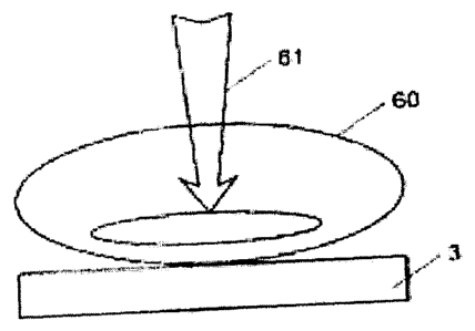
energies E; = hf, necessary for the synthesis of the material. Figure 5
illustrates how in the zone RI the energetic rays are introduced into the
chamber. Where applicable it is possible to polarise the rays that are
introduced into the chamber. In the latter case the direction of the wave
vector associated with the frequency value and the polarisation plane of
the wave vector associated with the crystallography of the material are
taken into consideration. The energy thus produced will be injected into
the plasma, where it will be able to be absorbed by the substances
carrying the reactive carbon atoms present in the plasma. Since close to
the substrate and to the surface thereof the plasma is focused, a better
CA 02806935 2013-01-29
18
energy interaction between the substances carrying the reactive carbon
atoms and the substrate, where the material already formed is present,
will be obtained.
An improvement can be obtained by activating the UVC ray
generators 17 which will selectively excite the substances contained in
the plasma. This makes it possible to increase the production in the
plasma of a selective form containing unsaturated molecules or radicals
and thus to increase the probability of energy absorption. These UVC
rays are introduced into the zone RAS, that is to say into the zone of the
grille. For the example of diamond, the 17 frequency values are injected
into the plasma according to the set of vectors L, W, and Four
beams in the direction of the vector L, three beams in the direction of the
vector W, seven beams in the direction of the vector E and three beams
in the direction of the vector Finally,
by means of the focusing system,
it is possible to form a plasma well 63 around the substrate carrier (zone
RD) in order thus to focus the substances containing reactive-carbon
atoms around the substrate.
The invention is of course not limited to the synthesis of
diamond and may be applied to other materials to be synthesised. Thus,
for example, the method according to the invention is applicable to the
doping of diamond with boron in order to produce a superconductor. The
condition for obtaining a superconductor is that the density of the atoms
nB > 3x10² atoms/cm3 (>600 ppm). In order obtain a superconductor the
method according to the invention is at the start similar to that described
for synthesising diamond. For effecting the doping of the diamond with
boron, a gas carrying boron is introduced into the chamber, for example
trimethylborane or boron trichloride or diborane, in particular diborane
(C2H6) in a proportion of 0.01-200 ppm with respect to the H2, more
particularly 1 ppm to 20 ppm. This boron-carrying gas is for example
introduced when the layer of diamond already has a thickness of at least
1 pm, in particular approximately 1 to 5 pm. A second photon beam at
CA 02806935 2013-01-29
. .
19
the frequency corresponding to the electron-photon interaction that
causes superconductivity is also injected into the chamber after the
physico-chemical synthesis by resonance of the diamond. In particular,
the second photon beam is divided into first and second fragments of the
second beam and the two fragments of photon beams corresponding to
the photon frequency due to the presence of boron and which leads to
the appearance of superconductivity are injected into the plasma. More
particularly the first fragment of the second photon beam in the direction
LO_( 1---4_ and I-->), and the second fragment of the photon beam in the
direction , of the set of directional vectors L, W, E, with an offset of 4
mV with respect to the value of the non-doped diamond. Fuller details on
the phonon mode LO are set out in the article by M Hoesch et al entitled
"Discovery of phonons causing superconductivity in diamonds looking for
room temperature ¨ superconductors in diamonds" which appeared in
JAEA R&D Review 2007, page 45.
A possible reduction in the power of the various photon beams
corresponding to the deposition of diamond can be envisaged,
proportional to the difference in energy for the bonds of type B-C with
respect to C-C. This reduction makes it possible for the growth of the
diamond not to dominate the formation of the superconductivity and thus
facilitates or weights the process of replacement of carbon (C) by boron
(B).
Another application of the method according to the invention
consists of doping diamond with boron in order to produce a type p
semiconductor. One condition for obtaining a semiconductor is that the
density of the atoms is ng < 1x10² atoms/cm3 (<600 ppm). A boron-
carrying gas is used similar to that used for forming the superconductor
but with a quantity of 0.01-100 ppm with respect to the H2, in particular
0.1 ppm to 10 ppm. A third photon beam at the frequency corresponding
to the electron-phonon interaction that causes semiconductivity is also
injected into the chamber after the physico-chemical synthesis by
CA 02806935 2013-01-29
. .
resonance of the diamond. In particular, the third photon beam is divided
into first and second fragments of the third beam and the fragments of
photon beams corresponding to the phonon frequency due to the
presence of the boron and which leads to the appearance of
5 semiconductivity are injected into the plasma. Thus the five photon
beams corresponding to the frequency of the phonons due the presence
of boron, responsible for semiconductivity, are injected into the plasma.
The first fragment formed from three beams that are injected in the
direction L and the second fragment comprise two beams that are
10 injected in the direction , of the set of directional vectors L, W, E, .
Just
like for the production of superconductors, a possible reduction in the
power can be envisaged.
Yet another application of the method according to the
invention consists of doping diamond with nitrogen (N) in order to
15 produce a type n semiconductor. One condition for the obtaining of a
semiconductor is that the density of the atoms is 25 to 2500 ppm. A
nitrogen-carrying gas is used, such as for example N2, CH3 or CH3NH2, in
particular N2, with a ratio of 0.1 to 1 of N2 with respect to CH.4. Photons
at the frequency corresponding to the electron-phonon interaction that
20 causes type n semiconductivity are also introduced into the chamber
after the physico-chemical synthesis by resonance of the diamond. In
particular the photon beams corresponding to the phonon frequency due
to the presence of nitrogen for the type C centre, and (or) the three
photon beams corresponding to the phonon frequency due to the
presence of nitrogen for the type A aggregate, and (or) the four photon
beams corresponding to the phonon frequency due to the presence of
nitrogen for the type B aggregate are in particular injected into the
plasma according to the set of directional vectors. Just as for the
production of type p semiconductors, a possible reduction in the power
can be envisaged.
The method according to the invention also makes it possible
CA 02806935 2013-01-29
21
to dope the diamond with phosphorus in order to produce a type n
semiconductor. A phosphorus-carrying gas is used, such as for example
phosphane (PH3) with a phosphorus/carbon mol ratio of 4*10-2 to 4'10-6,
in particular 2*10-2 to 1*10-3. A fourth photon beam at the frequency
corresponding to the electron-phonon interaction that causes type n
semiconductivity is also introduced into the chamber after the physico-
chemical synthesis by resonance of the diamond. In particular the
photon beams located at 523 meV and 562 meV and corresponding to
the phonon frequency due to the presence of phosphorus in the
crystalline lattice and responsible for semiconductivity are injected into
the plasma according to the set of directional vectors. A possible
reduction in the power can be envisaged.
The method according to the invention also makes it possible
to form by doping a semiconductor of the Si-Ge (silicon germanium) type.
It should be noted that, in the example of doping of Si by Ge, the epitaxy
of Ge on Si and the formation of an alloy of the Sii_xGex type in the CVD
process, leads to the appearance of tension in the interface and inside
the crystal due to the difference between the constant of the Si lattice
and that of Ge. These tensions are a source of defect in the crystalline
structure. Thus generally heteroepitaxy of Ge on Si begins with the
appearance of islands of Ge on the Si. These islands are in the form of
a pyramid and peaks that may lead as far as the formation of aggregates
of Ge. This has a consequence of forming a non-homogeneous deposit.
A deposit of Si and Ge is currently considered of high quality if
the density of defects due to the appearance of such deformations is
smaller than 0.3 particles/cm2 with a low density of dislocations smaller
than 106/cm2. The method according to the invention makes it possible
to form an Si-Ge deposit that will have fewer imperfections as described
and which may even eliminate them. To this end the method for a
deposition of Si-Ge comprises:
(a) a step of chemical vapour deposition (CVD) of silicon on a
CA 02806935 2013-01-29
. ,
22
pure silicon substrate or on a blank substrate, at a
temperature of between 500 C and 600 C, preferably at a
temperature (TO) of 500 C, in the presence of hydrogen. The
pressure in the chamber is preferably 0.01 mbar to 1000 mbar,
in particular 0.1 mbar to 1000 mbar, more particularly 1 mbar
to 800 mbar. As a silicon precursor gas use is made of
SiH2C12, SiHC13, SiCI4 or Si(CH3)4, in particular SiH4, until a
thickness of layer of 3 nm to 5 nm preferably is obtained. A
mixture of one or more of these precursor gases may also be
envisaged. To obtain a higher
deposition rate and a
deposition with a quality superior to that of the basic method,
the photon beam corresponding to the frequency of the
phonon due to the Si-Si bond is injected into the chamber
while pointing towards the substrate and according to the set
of directional vectors L, X, Z, After having obtained
the
desired thickness of layer the addition of SiHit is stopped, and
the temperature of the photon beam is reduced to 400 C to
550 C, preferably to 430 C to 460 C, in the presence of
hydrogen. The pressure in the chamber is preferably 0.01
mbar to 1000 mbar, in particular 1 mbar to 800 mbar;
(b) a step of stabilisation of the temperature of the substrate at a
first temperature (T1) from 400 C to 550 C, preferably 430 C
to 460 C, more particularly 450 C, in the presence of
hydrogen. The pressure in the chamber is preferably 0.01
mbar to 1000 mbar, in particular 1 mbar to 800 mbar;
(c) a step of chemical vapour deposition (CVD) of germanium at
the first temperature, referred to as T1, on the pure silicon
substrate or on the silicon substrate already obtained after
CVD of silicon, until a predetermined thickness of layer of
germanium is obtained, or a desired final layer thickness
obtained on the layer of silicon, the germanium precursor gas
CA 02806935 2013-01-29
. ,
23
is preferably GeH4. The photon beam corresponding to the
frequency of the phonon due to the Ge-Ge bond and the
photon beam corresponding to the frequency of the phonon
due the Si-Ge bond is then injected into the chamber while
pointing to the substrate, according to the set of directional
vectors L, W, Z,
The latter beam will act during the
formation of the first atomic layers of Ge, that is to say during
the formation of the Si-Ge interface. Subsequently the power
of the photon beam corresponding to this bond (Si-Ge) will be
reduced, or even decreased to zero, but while maintaining the
power of the photon beam corresponding to the Ge-Ge bond.
This will make it possible to obtain a reduction in the number
of defects in the deposition, that is to say to obtain a
deposition with a superior quality with a higher deposition rate.
This step is performed in the presence of hydrogen. The
pressure in the chamber is preferably 0.01 mbar to 1000 mbar,
in particular 1 mbar to 800 mbar;
and the optional steps:
(d1) ¨ a step in which the CVD of the germanium and the
photon beam correspond to the frequency of the phonon due
to the Ge-Ge bond is stopped, at a temperature below the
temperature (T2) as far as a third temperature (T3) of 500 C to
600 C, preferably 540 C to 560 C, in particular 550 C, a step
performed in the presence of hydrogen. The pressure in the
chamber is preferably 0.01 mbar to 1000 mbar, in particular 1
mbar to 800 mbar;
(d2) ¨ a step of CVD at the third temperature (T3) of an Sii_
xGex alloy, where x<0.9, until an intermediate layer of Sii_xGex
having the desired thickness is obtained. The germanium
precursor gas is preferably GeH4. The precursor gas for
silicon is SiH2C12, SiHCI3, SiCI4 and Si(CH3)4, in particular Sil-14.
CA 02806935 2013-01-29
. .
24
The photon beam (IR) and/or the two photon beams (IR and
Raman) corresponding to the frequencies of the phonons due
to the Si-Ge bond are next injected into the chamber by
pointing to the substrate and according to the set of directional
vectors L, W, I, This step is performed
in the presence of
hydrogen. The pressure in the chamber is preferably 0.01
mbar to 1000 mbar, in particular 1 mbar to 800 mbar;
(d3) a transition step, at the third temperature (T3), in which
the CVD of the Sii_xGex alloy changes to a pure germanium
CVD. The flow of silicon precursor gas is stopped in order to
achieve the change to the following step. The photon beam or
beams corresponding to the frequency of the phonon due to
the Si-Ge bond are also stopped in order to inject the photon
beam corresponding to the frequency of the phonon due to the
Ge-Ge bond. The change from the
photon beam
corresponding to the frequency of the phonon due to the Si-
Ge bond to the photon corresponding to the frequency of the
phonon due to the Ge-Ge bond must preferably take place in
a synchronised fashion, preferably by simultaneous
decrementing-incrementing of the power, a step carried out in
the presence of hydrogen. The pressure in the chamber is
preferably 0.01 mbar to 1000 mbar, in particular 1 mbar to 800
mbar;
(d4) ¨ a step in which the CVD of the germanium is
maintained at this temperature (T3) so as to obtain the
deposition of germanium as a top layer and Sii_xGex as an
intermediate layer.
During this step the photon beam
corresponding to the frequency of the phonon due to the Ge-
Ge bond is maintained. This step is performed in the
presence of hydrogen and the pressure in the chamber is
preferably 0.01 mbar to 1000 mbar, preferably 1 mbar to 800
CA 02806935 2013-01-29
. .
mbar;
(d5) ¨ a step in which the germanium CVD temperature is
increased from the third temperature (T3) to a fourth
temperature (T4) of 750 C to 850 C , preferably 800 C to
5 850 C.
During this step the photon beam corresponding to the
frequency of the phonon due the Ge-Ge bond is maintained.
T4 is preferably equal to T2, and the step is performed in the
presence of hydrogen, the pressure in the chamber is
preferably 0.01 mbar to 1000 mbar, in particular 1 mbar to 800
10 mbar;
(e) a step of incrementing the temperature of the chemical vapour
deposition (CVD) of the germanium from the first temperature (T1) to a
second temperature (T2) limited to 750 C to 850 C, preferably 800 C to
850 C. This step is performed without the presence of the photon beam
15
corresponding to the frequency of the phonon due to the Ge-Ge bond.
This step is however performed in the presence of hydrogen. The
pressure in the chamber is preferably 0.01 mbar to 1000 mbar, in
particular 1 mbar to 800 mbar;
(f) continuation of the germanium CVD at the second temperature (T2)
20 until the
desired thickness of the layer of germanium. The photon beam
corresponding to the frequency of the phonon due to the Ge-Ge bond is
maintained. This step is performed in the presence of hydrogen and the
pressure in the chamber is preferably 0.01 mbar to 1000 mbar, in
particular 1 mbar to 800 mbar.