Note: Descriptions are shown in the official language in which they were submitted.
CA 02807392 2013-02-01
WO 2012/018918 PCT/US2011/046429
1
GENERATING A NON-REVERSIBLE STATE AT A BITCELL HAVING A
FIRST MAGNETIC TUNNEL JUNCTION AND A SECOND MAGNETIC
TUNNEL JUNCTION
I. Field
[0001] The present disclosure is generally related to a magnetic tunnel
junction based
one-time programmable bitcell.
IL Description of Related Art
[0002] Advances in technology have resulted in smaller and more powerful
computing
devices. Such portable computing devices may include security architectures
based on
one-time programmable elements, such as a nonvolatile memory device having one-
time programmable (OTP) memory cells. An OTP memory cell maintains a permanent
state once the cell is programmed. For example, polysilicon fuses have been
used as
OTP elements. A polysilicon fuse memory cell can be programmed by applying a
voltage across the cell so that the cell is "blown" during programming. For
example,
one-time programming is typically performed by blowing the silicon with a high
current
(e.g., on order of milliamperes) for a relatively long time (e.g.,
microseconds). One
drawback of polysilicon fuses is that the integrity of the fuse is difficult
to test before
blowing the fuse. Another drawback of polysilicon fuses is that a blown state
is visibly
detectable, which may compromise security.
III. Summary
[0003] A one-time programmable element based on magnetic tunnel junction
(MTJ)
technology is described. The one-time programmable element is configured as a
bitcell
having a first resistive memory element and a second resistive memory element.
The
first and second resistive memory elements may each be MTJs. The native un-
blown
state of a MTJ has a higher resistance and the blown state of an MTJ has a
lower
resistance. A program signal can be applied to one of the first MTJ and the
second MTJ
without applying the program signal to the other one of the first MTJ and the
second
MTJ to generate a non-reversible state at the bitcell. For example, the non-
reversible
state may be generated by breaking down a tunnel oxide of one of the MTJs.
When the
tunnel oxide is broken down, a permanent low resistance state is created.
CA 02807392 2014-01-31
74769-3494
2
[0004] In a particular embodiment, a method of generating a non-
reversible state at a
bitcell having a first magnetic tunnel junction (MTJ) and a second MTJ
includes applying a
program voltage to the first MTJ of the bitcell without applying the program
voltage to the
second MTJ of the bitcell.
[0005] In another particular embodiment, a memory device includes a
magnetic tunnel
junction (MTJ) bitcell. The MTJ bitcell includes a first MTJ, a second MTJ,
and
programming circuitry configured to generate a non-reversible state at the
bitcell by applying
a program signal to a selected one of the first MTJ and the second MTJ of the
bitcell.
[0006] One particular advantage provided by at least one of the
disclosed
embodiments is that high speed programming may be achieved by a non-reversible
state being
programmed to a bitcell having a first magnetic tunnel junction (MTJ) and a
second MTJ.
[0007] Another particular advantage provided by at least one of the
disclosed
embodiments is that prior to programming, operation of the bitcell may be
tested.
[0008] Another particular advantage provided by at least one of the
disclosed
embodiments is enhanced security in that visible detection of a programmed
state of the
bitcell is more difficult than for polysilicon fuses.
[0008a] According to one aspect of the present invention, there is
provided a method
comprising: generating a non-reversible state at a bitcell by applying a
program voltage to a
first magnetic tunnel junction (MTJ) of the bitcell without applying the
program voltage to a
second MTJ of the bitcell, wherein the non-reversible state corresponds to a
value of the
bitcell that is determined by comparing a first value read at the first MTJ to
a second value
read at the second MTJ.
[0008b] According to another aspect of the present invention, there is
provided a
method comprising: a first step for generating a non-reversible state at a
bitcell by applying a
program voltage to a first magnetic tunnel junction (MTJ) of the bitcell
without applying the
program voltage to a second MTJ of the bitcell, wherein the non-reversible
state corresponds
CA 02807392 2014-01-31
74769-3494
2a
to a value of the bitcell that is determined by comparing a first value read
at the first MTJ to a
second value read at the second MTJ; and a second step for maintaining the
first MTJ and the
second MTJ as complementary cell values.
10008c1 According to still another aspect of the present invention,
there is provided a
method comprising: receiving design information representing at least one
physical property
of a semiconductor device, the semiconductor device comprising: a magnetic
tunnel junction
(MTJ) bitcell comprising: a first MTJ; and a second MTJ; programming circuitry
configured
to generate a non-reversible state at the bitcell by applying a program signal
to a selected one
of the first MTJ and the second MTJ of the bitcell; and sensing circuitry
configured to sense
the non-reversible state by comparing a first value read at the first MTJ to a
second value read
at the second MTJ; transforming the design information to comply with a file
format; and
generating a data file comprising the transformed design information.
[0008d] According to yet another aspect of the present invention,
there is provided a
method comprising: receiving a data file comprising design information
corresponding to a
semiconductor device; and fabricating the semiconductor device according to
the design
information, wherein the semiconductor device comprises: a magnetic tunnel
junction (MTJ)
bitcell including: a first MTJ; and a second MTJ; programming circuitry
configured to
generate a non-reversible state at the bitcell by applying a program signal to
a selected one of
the first MTJ and the second MTJ of the bitcell; and sensing circuitry
configured to sense the
non-reversible state by comparing a first value read at the first MTJ to a
second value read at
the second MTJ.
[0009] Other aspects, advantages, and features of the present
disclosure will become
apparent after review of the entire application, including the following
sections: Brief
Description of the Drawings, Detailed Description, and the Claims.
CA 02807392 2014-01-31
74769-3494
2b
IV. Brief Description of the Drawings
[0010] FIG. 1 is a block diagram of a particular illustrative
embodiment of a memory
device including non-reversible state programming circuitry and a memory cell
including a
first resistive memory element and a second resistive memory element;
[0011] FIG. 2 is a diagram of a particular illustrative embodiment of a
memory device
including non-reversible state programming circuitry and a memory array with
magnetic
tunnel junction (MTJ)-based one-time programmable memory cells;
CA 02807392 2013-02-01
WO 2012/018918 PCT/US2011/046429
3
[0012] FIG. 3 is a diagram of a particular illustrative embodiment of a
system including
a bitcell having a first MTJ and a second MTJ and non-reversible state
programming
circuitry configured to provide a programming voltage to the bitcell;
[0013] FIG. 4 is a diagrammatic representation of particular illustrative
embodiments of
MTJ shapes and attributes of each MTJ shape;
[0014] FIG. 5 is a flow diagram of a particular illustrative embodiment of
a method of
programming a non-reversible state to a bitcell having a first MTJ and a
second MTJ;
[0015] FIG. 6 is a block diagram of a particular illustrative embodiment
of a device
including non-reversible state programming circuitry configured to provide a
programming voltage to one of a first MTJ and a second MTJ of a bitcell; and
[0016] FIG. 7 is a diagram of a particular illustrative embodiment of a
manufacturing
process that may be used to produce a wireless device including non-reversible
state
programming circuitry configured to program a non-reversible state to a
bitcell having a
first MTJ and a second MTJ.
V. Detailed Description
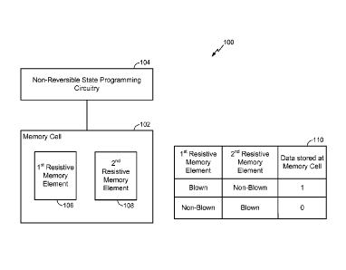
[0017] Referring to FIG. 1, a particular illustrative embodiment of a
memory device
including non-reversible state programming circuitry and a memory cell to
store data as
non-reversible states in dual-element cells is depicted and generally
designated 100.
The memory device 100 includes a representative memory cell 102 and non-
reversible
state programming circuitry 104. The memory cell 102 includes a first
resistive
memory element 106 and a second resistive memory element 108. In a particular
embodiment, the first resistive memory element 106 is a first magnetic tunnel
junction
(MTJ) element and the second resistive memory element 108 is a second MTJ
element.
The non-reversible state programming circuitry 104 is configured to apply a
program
signal to one of the first resistive memory element 106 and the second
resistive memory
element 108 of the memory cell 102 to program a non-reversible state to the
memory
cell 102.
[0018] In a particular embodiment, one-time programmability is achieved by
non-
reversibly programming one of the two resistive memory elements 106, 108 in
the
memory cell 102. For example, a program voltage may be applied to the first
resistive
CA 02807392 2013-02-01
WO 2012/018918 PCT/US2011/046429
4
memory element 106 of the memory cell 102 via the non-reversible state
programming
circuitry 104 without applying the program voltage to the second resistive
memory
element 108 of the memory cell 102 to generate a non-reversible state at the
memory
cell 102. Alternatively, a program voltage may be applied to the second
resistive
memory element 108 of the memory cell 102 via the non-reversible state
programming
circuitry 104 without applying the program voltage to the first resistive
memory element
106 of the memory cell 102 to generate a non-reversible state at the memory
cell 102.
To illustrate, when the first resistive memory element 106 is an MTJ, the
program
voltage may cause a tunnel oxide of the first resistive memory element 106 to
break
down resulting in a permanent low resistance state of the first resistive
memory element
106. Similarly, when the second resistive memory element 108 is an MTJ, the
program
voltage may cause a tunnel oxide of the second resistive memory element 108 to
break
down resulting in a permanent low resistance state of the second resistive
memory
element 108. In a particular embodiment, the tunnel oxide may be a magnesium
oxide
barrier layer within an MTJ and the program voltage may be greater than
approximately
1.3 volts.
[0019] When the tunnel oxide of one of the resistive memory elements is
broken down,
a permanent low-resistance state is created. For example, once blown (e.g.,
once the
tunnel oxide is broken down), a resistance of the blown resistive memory
element may
be approximately 250 ohms. A native un-blown state of a resistive memory
element
may be a higher resistance, for example 2500 ohms. For example, as illustrated
in table
110, if the first resistive memory element 106 is blown and the second
resistive memory
element 108 is non-blown, the data stored at the memory cell 102 may represent
a logic
"1" state. Alternatively, if the first resistive memory element 106 is non-
blown and the
second resistive memory element 108 is blown, the data stored at the memory
cell 102
may represent a logic "0" state.
[0020] In a particular embodiment, prior to programming a non-reversible
state to the
memory cell 102, the memory cell 102 may be used as a many-time programmable
(MTP) cell by applying a write voltage (as opposed to a program voltage) to
the first
resistive memory element 106 or to the second resistive memory element 108 to
store a
reversible value to the memory cell 102. Examples of MTP cells are further
described
with respect to FIG. 4. Use of the memory cell 102 as a one-time programmable
(OTP)
CA 02807392 2013-02-01
WO 2012/018918 PCT/US2011/046429
cell or a MTP cell enables testing of an operation of the memory cell 102 by
reading a
respective one of the first resistive memory element 106 and the second
resistive
memory element 108 after applying the write voltage to the first resistive
memory
element 106 or to the second resistive memory element 108.
[0021] In a particular embodiment, when the memory cell 102 is configured
as an OTP
memory cell, the non-reversible state may be sensed by comparing a value read
at the
first resistive memory element 106 to a value read at the second resistive
memory
element 108 without the need for a separate reference cell. For example, in
order to
sense a reversible write state of an MTJ, a reference voltage may be applied.
When the
memory cell 102 is configured as an OTP memory cell, the sensing is self-
referenced in
that complementary cell values are maintained at the first and second
resistive memory
elements 106, 108, such that the non-reversible state can be sensed by
comparing a
value read at the first resistive memory element 106 to a value read at the
second
resistive memory element 108.
[0022] Because the memory cell 102 may be configured as an OTP memory cell
or a
MTP memory cell, security architectures of electronic devices that incorporate
the
memory cell may be enhanced. For example, hardware features of a mobile
electronic
device such as joint test action group (JTAG) may be disabled after final test
using one-
time programmability. In addition, original equipment manufacturer hardware
keys
may be utilized with one-time programmability for provisioning, user
information,
digital rights management, etc. In addition, electronic devices that
incorporate the
memory cell 102 may be less susceptible to tampering due to de-processing and
less
susceptible to data manipulation than polysilicon based fuse systems.
[0023] Referring to FIG. 2, a particular illustrative embodiment of a
memory device
including non-reversible state programming circuitry and a memory array with
magnetic
tunnel junction (MTJ)-based one-time programmable memory cells is depicted and
generally designated 200. The memory device 200 includes non-reversible state
programming circuitry 202, test circuitry 204, and a memory array 206 with one-
time
programmable (OTP) cells. The memory array 206 may include other memory cells,
such as other MTJ memory cells, that are non-OTP memory cells. The OTP memory
cells and the other MTJ memory cells may be manufactured using the same
techniques.
The memory array 206 includes a representative first one-time programmable
cell 208
CA 02807392 2013-02-01
WO 2012/018918
PCT/US2011/046429
6
and a representative second one-time programmable cell 210. In a particular
embodiment, the first one-time programmable cell 208 comprises a first dual-
magnetic
tunnel junction (MTJ) bitcell and the second one-time programmable cell 210
comprises
a second dual-MTJ bitcell. The first one-time programmable cell 208 includes a
first
resistive memory element 212, a first access transistor 213, a second
resistive memory
element 214, and a second access transistor 215. The second one-time
programmable
cell 210 includes a third resistive memory element 216, a third access
transistor 217, a
fourth resistive memory element 218, and a fourth access transistor 219. In a
particular
embodiment, each of the resistive memory elements 212-218 comprises a magnetic
tunnel junction element. A word line 220 is coupled to the first access
transistor 213, to
the second access transistor 215, to the third access transistor 217, and to
the fourth
access transistor 219.
[0024] The
non-reversible state programming circuitry 202 is coupled to the first one-
time programmable cell 208 via bitline 230 and bitline 232 and to the second
one-time
programmable cell 210 via bitline 240 and bitline 242. The non-reversible
state
programming circuitry 202 is configured to apply a program voltage via the
bitline 230
to the first resistive memory element 212 of the first one-time programmable
cell 208
without applying the program voltage to the second resistive memory element
214 of
the first one-time programmable cell 208 to generate a first non-reversible
state (e.g.
logic "0") at the first one-time programmable cell 208. Alternatively, the non-
reversible
state programming circuitry 202 may apply the program voltage via the bitline
232 to
the second resistive memory element 214 of the first one-time programmable
cell 208
without applying the program voltage to the first resistive memory element 212
of the
first one-time programmable cell 208 to generate a second non-reversible state
(e.g.
logic "1") at the first one-time programmable cell 208.
[0025]
Similarly, the non-reversible state programming circuitry 202 is configured to
apply the program voltage via the bitline 240 to the third resistive memory
element 216
of the second one-time programmable cell 210 without applying the program
voltage to
the fourth resistive memory element 218 of the second one-time programmable
cell 210
to generate the first non-reversible state at the second one-time programmable
cell 210.
Alternatively, the non-reversible state programming circuitry 202 may apply
the
program voltage via the bitline 242 to the fourth resistive memory element 218
of the
CA 02807392 2013-02-01
WO 2012/018918 PCT/US2011/046429
7
second one-time programmable cell 210 without applying the program voltage to
the
third resistive memory element 216 of the second one-time programmable cell
210 to
generate the second non-reversible state at the second one-time programmable
cell 210.
[0026] In a particular embodiment, the non-reversible state may be sensed
at the first
one-time programmable cell 208 by comparing a value read at the first
resistive memory
element 212 to a value read at the second resistive memory element 214. In a
particular
embodiment, the non-reversible state of the first one-time programmable cell
may be
sensed without a separate reference cell.
[0027] For example, the sensing of the first one-time programmable cell
208 is self-
referenced in that complementary cell values are maintained at the first and
second
resistive memory elements 212, 214 (e.g., the tunnel oxide of one of the
resistive
memory elements 212, 214 is blown while the tunnel oxide of the other one of
the
resistive memory elements 212, 214 is non-blown). The non-reversible state can
be
sensed by comparing a value read at the first resistive memory element 212 to
a value
read at the second resistive memory element 214 (e.g., by comparing a signal
at the
bitline 230 to a signal at the bitline 232). There is no need for a separate
reference
voltage to sense the reversible states of the resistive memory elements 212,
214.
[0028] The test circuitry 204 may be configured to test one or more cells
of the memory
array 206 prior to programming. For example, prior to applying the program
voltage to
the first resistive memory element 212 of the first one-time programmable cell
208, a
write voltage may be applied to the first resistive memory element 212 to
store a
reversible value to the first one-time programmable cell 208. After applying
the write
voltage to the first resistive memory element 212, the first resistive memory
element
212 may be read to test an operation of the first one-time programmable cell
208.
Alternatively, prior to applying the program voltage to the second resistive
memory
element 214 of the first one-time programmable cell 208, a write voltage may
be applied
to the second resistive memory element 214 to store a reversible value to the
first one-
time programmable cell 208. After applying the write voltage to the second
resistive
memory element 214, the second resistive memory element 214 may be read to
test an
operation of the first one-time programmable cell 208.
CA 02807392 2013-02-01
WO 2012/018918 PCT/US2011/046429
8
[0029] In a particular embodiment, the third resistive memory element 216
and the
fourth resistive memory element 218 may be substantially similar to the first
resistive
memory element 212 and the second resistive memory element 214. In a
particular
embodiment, the resistive memory elements 216 and 218 may be used as many-time
programmable memory elements by providing a write voltage where the write
voltage is
lower than the program voltage (e.g., has a lower magnitude than the program
voltage),
causing the resistive memory element 216 or 218 to enter a reversible state.
[0030] By using MTJ elements in the bitcells of a memory array for one-
time
programmability, high speed programming may be achieved due to the smaller
currents
and shorter times needed to program the MTJ elements as compared to the larger
currents and longer times needed to program polysilicon fuse elements.
[0031] Referring to FIG. 3, a particular illustrative embodiment of a
system 300
includes a bitcell 302 having a first resistive memory element 310 and a
second resistive
memory element 314 and also including non-reversible state programming
circuitry 304
configured to provide a programming voltage to the bitcell 302.
[0032] The programming circuitry 304 includes read column select circuitry
320, sense
amplifier circuitry 322, word line generation circuitry 324, write data path
circuitry 326,
write data circuitry 328, write column select circuitry 330, and a pair of
bitlines 332.
The read column select circuitry 320 is configured to receive address data 340
and read
data 342, and to provide an input to the sense amplifier circuitry 322. The
sense
amplifier circuitry 322 is configured to amplify a differential signal at the
pair of
bitlines 332 and to generate a data output signal (Do). The write data
circuitry 328 is
configured to latch received data input (Di) 362 and a write signal 360. The
write
column select circuitry 330 is configured to latch received address data 340.
The write
data path circuitry 326 is responsive to the write data circuitry 328 and the
write column
select circuitry 330 to apply signals to the pair of bitlines 332. The word
line generation
circuitry 324 is configured to selectively bias a word line 334 in response to
the address
data 340, a read signal 350, and the write signal 360.
[0033] The bitcell 302 includes the first resistive memory element 310 and
the second
resistive memory element 314. In a particular embodiment, the first resistive
memory
element 310 comprises a first magnetic tunnel junction (MTJ) and the second
resistive
CA 02807392 2013-02-01
WO 2012/018918 PCT/US2011/046429
9
memory element comprises a second MTJ. The bitcell 302 includes a first access
transistor 312 coupled to the first MTJ 310 and a second access transistor 316
coupled
to the second MTJ 314. In a particular embodiment, the first access transistor
312 may
have a tunnel oxide with oxide thickness Ti 311 and the second access
transistor 316
may have a tunnel oxide with oxide thickness T2 315. The oxide thickness Ti
311 may
be substantially similar to the oxide thickness T2 315. The first access
transistor 312
and the second access transistor 316 are responsive to the word line 334.
[0034] During operation, the non-reversible state programming circuitry
304 can apply
a program voltage to the first MTJ 310 of the bitcell 302 without applying the
program
voltage to the second MTJ 314 of the bitcell 302 to generate a non-reversible
state at the
bitcell 302. Alternatively, the non-reversible state programming circuitry 304
can apply
the program voltage to the second MTJ 314 of the bitcell 302 without applying
the
program voltage to the first MTJ 310 of the bitcell 302 to generate the non-
reversible
state at the bitcell 302.
[0035] For example, in a particular embodiment, the program voltage may
cause the
tunnel oxide of the first MTJ 310 to break down resulting in a permanent low
resistance
state of the first MTJ 310. In a particular embodiment, the tunnel oxide may
be a
magnesium oxide barrier layer and the program voltage may be greater than
approximately 1.3 volts. After the tunnel oxide of the first MTJ 310 is broken
down, a
permanent short or low resistance state of the first MTJ 310 is created. For
example,
once blown, a resistance of the blown first MTJ 310 may be approximately 250
ohms.
A native un-blown state of the second MTJ 314 may be a higher resistance, for
example
2500 ohms. In a particular embodiment, a state of the first MTJ 310 (e.g.,
blown) may
be maintained as complementary to a state of the second MTJ 314 (e.g., un-
blown). The
sensing of the bitcell 302 is self-referenced in that the non-reversible state
can be sensed
by comparing a value read at the first MTJ 310 to a value read at the second
MTJ 314
(e.g., by comparing a signal at the pair of bitlines 332) without a separate
reference
voltage.
[0036] Referring to FIG. 4, particular illustrative embodiments of shapes
for a one-time
programmable magnetic tunnel junction (MTJ) bitcell are depicted and generally
designated 400. A first MTJ has a substantially ellipsoidal shape 402, a
second MTJ
has a substantially circular shape 404, and a third MTJ has a substantially
circular shape
CA 02807392 2013-02-01
WO 2012/018918 PCT/US2011/046429
406 smaller than the second MTJ. Arrows illustrate examples of magnetic
moments of
a free layer of each of the MTJs 402-406 as illustrative, non-limiting
examples.
[0037] The MTJ with the ellipsoidal shape 402 has a bi-stable state when
the MTJ 402
is non-blown. When in the bi-stable state, the MTJ 402 may have either a low
resistance R Low (e.g., approximately 2500 ohms) or a high resistance R High
(e.g.,
greater than 3000 ohms). In a blown state, the MTJ 402 may have a resistance
at a
blown resistance R Blown (e.g., approximately 250 ohms). In a particular
embodiment,
the ellipsoidal MTJ 402 has a first axis length 403 greater than a second axis
length 405
to enable alignment of magnetic moments in the MTJ 402 in parallel and anti-
parallel
states, corresponding to a first reversible many-time programmable (MTP) state
and a
second reversible MTP state.
[0038] In a particular embodiment, the second MTJ with the circular shape
404 is in a
mono-stable state when the second MTJ 404 is non-blown. For example, in the
non-
blown state, the second MTJ 404 may have a resistance halfway between the high
resistance R High (e.g., greater than 3000 ohms) of the second MTJ 404 and the
low
resistance R Low (e.g., 2500 ohms) of the second MTJ 404. In the blown state,
the
second MTJ 404 may have a resistance at the blown resistance R Blown (e.g.,
approximately 250 ohms).
[0039] In a particular embodiment, the third MTJ with the circular shape
406 has a
smaller diameter than that of the circular MTJ 404 such that the third MTJ 406
is in a
meta-stable state when the third MTJ 406 is non-blown. For example, in the non-
blown
state, the third MTJ 406 may have a resistance at a point between the high
resistance R
High (e.g., greater than 3000 ohms) of the third MTJ 406 and the low
resistance R Low
(e.g., 2500 ohms) of the third MTJ 406. In the blown state, the third MTJ 406
may have
a resistance at the blown resistance R Blown (e.g., approximately 250 ohms).
[0040] Referring to FIG. 5, a flow diagram of an illustrative embodiment
of a method of
programming a non-reversible state to a bitcell having a first magnetic tunnel
junction
(MTJ) and a second MTJ is depicted and generally designated 500. As an
illustrative
example, the method 500 may be performed by the memory device of FIG. 1, the
memory device of FIG. 2, the system of FIG. 3, or any combination thereof.
CA 02807392 2013-02-01
WO 2012/018918 PCT/US2011/046429
11
[0041] Prior to applying a program voltage to the bitcell, a write voltage
may be applied
to the first MTJ to store a reversible value to the bitcell, at 502, and the
first MTJ may
be read to test an operation of the bitcell after applying the write voltage
to the first
MTJ, at 504. In a particular embodiment, the bitcell may be the memory cell
102 of
FIG. 1, the first one-time programmable cell 208 of FIG. 2, or the bitcell 302
of FIG. 3.
In a particular embodiment, the first MTJ may be the first resistive memory
element 106
of FIG. 1, the first resistive memory element 212 of FIG. 2, or the first
resistive memory
element 310 of FIG. 3, and the second MTJ may be the second resistive memory
element 108 of FIG. 1, the second resistive memory element 214 of FIG. 2, or
the
second resistive memory element 314 of FIG. 3.
[0042] For example, the test circuitry 204 may be configured to test one
or more cells of
the memory array 206 prior to programming any of the cells of the memory array
206.
For example, prior to applying the program voltage, a write voltage may be
applied to
the first resistive memory element 212 to store a reversible value to the
first one-time
programmable cell 208. After applying the write voltage to the first resistive
memory
element 212, the first resistive memory element 212 may be read to test an
operation of
the first one-time programmable cell 208. Alternatively, the write voltage may
be
applied to the second resistive memory element 214 to store a reversible value
to the
first one-time programmable cell 208. After applying the write voltage to the
second
resistive memory element 214, the second resistive memory element 214 may be
read to
test an operation of the first one-time programmable cell 208.
[0043] A non-reversible state may be generated at the bitcell by applying
the program
voltage to the first MTJ of the bitcell without applying the program voltage
to the
second MTJ of the bitcell, at 506. In a particular embodiment, the program
voltage may
be generated by the non-reversible state programming circuitry 104 of FIG. 1,
the non-
reversible state programming circuitry 202 of FIG. 2, or the non-reversible
state
programming circuitry 304 of FIG. 3.
[0044] The first MTJ and the second MTJ may be maintained as complementary
cell
values, at 508. For example, in a particular embodiment, the program voltage
may
cause a tunnel oxide, such as the tunnel oxide having thickness Ti 311 of the
first MTJ
310 to break down, resulting in a permanent low resistance state of the first
MTJ 310.
After the tunnel oxide of the first MTJ 310 is broken down, a permanent short
or low
CA 02807392 2013-02-01
WO 2012/018918 PCT/US2011/046429
12
resistance state of the first MTJ 310 is created. For example, once blown, a
resistance
of the blown first MTJ 310 may be approximately 250 ohms. A native un-blown
state
of the second MTJ 314 may be a higher resistance, for example 2500 ohms. As
such, a
cell value of the first MTJ 310 (e.g., blown) may be maintained as
complementary to a
cell value of the second MTJ 314 (e.g., un-blown).
[0045] The non-reversible state may be sensed by comparing a value read at
the first
MTJ to a value read at the second MTJ of the bitcell, at 510. For example, the
sense
amplifier circuitry 322 may be configured to generate the output Do in
response to
comparing a signal (e.g., a current or a voltage) read at the first MTJ 310
and a signal
read at the second MTJ 314.
[0046] FIG. 6 is a block diagram of an embodiment of a wireless
communication device
600 having non-reversible state programming circuitry and a bitcell including
a first
magnetic tunnel junction (MTJ) and a second MTJ 664. The wireless
communication
device 600 may be implemented as a portable wireless electronic device that
includes a
processor 610, such as a digital signal processor (DSP), coupled to a memory
632.
[0047] The non-reversible state programming circuitry and bitcell
including first and
second MTJs 664 may include one or more of the components, memories, or
circuits of
FIGs. 1-4, operates in accordance with FIG. 5, or any combination thereof. The
non-
reversible state programming circuitry and bitcell including first and second
MTJs 664
may be in the memory 632 or may be a separate device. Although the non-
reversible
state programming circuitry and bitcell including first and second MTJs 664 is
illustrated integrated with the memory 632, in other embodiments the non-
reversible
state programming circuitry and bitcell including first and second MTJs 664
may be
external to the memory 632, such as embedded in the processor 610.
[0048] In a particular embodiment, a display controller 626 is coupled to
the processor
610 and to a display device 628. A coder/decoder (CODEC) 634 can also be
coupled to
the processor 610. A speaker 636 and a microphone 638 can be coupled to the
CODEC
634. A wireless controller 640 can be coupled to the processor 610 and to a
wireless
antenna 642.
[0049] The memory 632 may include a computer readable medium that stores
instructions (e.g., software 635) that are executable by a processor, such as
the processor
CA 02807392 2013-02-01
WO 2012/018918 PCT/US2011/046429
13
610. For example, the software 635 may include instructions that are
executable by a
computer to apply a program voltage to a first MTJ (e.g., the first resistive
memory
element 106 of FIG. 1) of a bitcell (e.g., the memory cell 102 of FIG. 1)
without
applying the program voltage to a second MTJ (e.g., the second resistive
memory
element 108 of FIG. 1) of the bitcell to generate a non-reversible state at
the bitcell.
[0050] In a particular embodiment, the signal processor 610, the display
controller 626,
the memory 632, the CODEC 634, and the wireless controller 640 are included in
a
system-in-package or system-on-chip device 622. In a particular embodiment, an
input
device 630 and a power supply 644 are coupled to the system-on-chip device
622.
Moreover, in a particular embodiment, as illustrated in FIG. 6, the display
device 628,
the input device 630, the speaker 636, the microphone 638, the wireless
antenna 642,
and the power supply 644 are external to the system-on-chip device 622.
However,
each of the display device 628, the input device 630, the speaker 636, the
microphone
638, the wireless antenna 642, and the power supply 644 can be coupled to a
component
of the system-on-chip device 622, such as an interface or a controller.
[0051] The foregoing disclosed devices and functionalities may be designed
and
configured into computer files (e.g. RTL, GDSII, GERBER, etc.) stored on
computer
readable media. Some or all such files may be provided to fabrication handlers
who
fabricate devices based on such files. Resulting products include
semiconductor wafers
that are then cut into semiconductor die and packaged into a semiconductor
chip. The
chips are then employed in devices described above.
[0052] FIG. 7 depicts a particular illustrative embodiment of an
electronic device
manufacturing process 700. Physical device information 702 is received at the
manufacturing process 700, such as at a research computer 706. The physical
device
information 702 may include design information representing at least one
physical
property of a semiconductor device, such as the memory device 100 of FIG. 1,
the
memory device 200 of FIG. 2, the system 300 of FIG. 3, or any combination
thereof.
For example, the physical device information 702 may include physical
parameters,
material characteristics, and structure information that is entered via a user
interface 704
coupled to the research computer 706. The research computer 706 includes a
processor
708, such as one or more processing cores, coupled to a computer readable
medium
such as a memory 710. The memory 710 may store computer readable instructions
that
CA 02807392 2013-02-01
WO 2012/018918
PCT/US2011/046429
14
are executable to cause the processor 708 to transform the physical device
information
702 to comply with a file format and to generate a library file 712.
[0053] In a particular embodiment, the library file 712 includes at least
one data file
including the transformed design information. For example, the library file
712 may
include a library of semiconductor devices including a device that includes
the memory
device 100 of FIG. 1, a device that includes the memory device 200 of FIG. 2,
a device
that includes the system 300 of FIG. 3, or any combination thereof, that is
provided to
use with an electronic design automation (EDA) tool 720.
[0054] The library file 712 may be used in conjunction with the EDA tool
720 at a
design computer 714 including a processor 716, such as one or more processing
cores,
coupled to a memory 718. The EDA tool 720 may be stored as processor
executable
instructions at the memory 718 to enable a user of the design computer 714 to
design a
circuit including a device that includes the memory device 100 of FIG. 1, a
device that
includes the memory device 200 of FIG. 2, a device that includes the system
300 of
FIG. 3, or any combination thereof, of the library file 712. For example, a
user of the
design computer 714 may enter circuit design information 722 via a user
interface 724
coupled to the design computer 714. The circuit design information 722 may
include
design information representing at least one physical property of a
semiconductor
device, such as a device that includes the memory device 100 of FIG. 1, a
device that
includes the memory device 200 of FIG. 2, a device that includes the system
300 of
FIG. 3, or any combination thereof. To illustrate, the circuit design property
may
include identification of particular circuits and relationships to other
elements in a
circuit design, positioning information, feature size information,
interconnection
information, or other information representing a physical property of a
semiconductor
device.
[0055] The design computer 714 may be configured to transform the design
information, including the circuit design information 722, to comply with a
file format.
To illustrate, the file formation may include a database binary file format
representing
planar geometric shapes, text labels, and other information about a circuit
layout in a
hierarchical format, such as a Graphic Data System (GDSII) file format. The
design
computer 714 may be configured to generate a data file including the
transformed
design information, such as a GDSII file 726 that includes information
describing the
CA 02807392 2013-02-01
WO 2012/018918 PCT/US2011/046429
memory device 100 of FIG. 1, the memory device 200 of FIG. 2, the system 300
of FIG.
3, or any combination thereof, in addition to other circuits or information.
To illustrate,
the data file may include information corresponding to a system-on-chip (SOC)
that
includes the memory device 100 of FIG. 1 and that also includes additional
electronic
circuits and components within the SOC.
[0056] The GDSII file 726 may be received at a fabrication process 728 to
manufacture
the memory device 100 of FIG. 1, the memory device 200 of FIG. 2, the system
300 of
FIG. 3, or any combination thereof, according to transformed information in
the GDSII
file 726. For example, a device manufacture process may include providing the
GDSII
file 726 to a mask manufacturer 730 to create one or more masks, such as masks
to be
used with photolithography processing, illustrated as a representative mask
732. The
mask 732 may be used during the fabrication process to generate one or more
wafers
734, which may be tested and separated into dies, such as a representative die
736. The
die 736 includes a circuit including a device that includes the memory device
100 of
FIG. 1, a device that includes the memory device 200 of FIG. 2, a device that
includes
the system 300 of FIG. 3, or any combination thereof
[0057] The die 736 may be provided to a packaging process 738 where the
die 736 is
incorporated into a representative package 740. For example, the package 740
may
include the single die 736 or multiple dies, such as a system-in-package (SiP)
arrangement. The package 740 may be configured to conform to one or more
standards
or specifications, such as Joint Electron Device Engineering Council (JEDEC)
standards.
[0058] Information regarding the package 740 may be distributed to various
product
designers, such as via a component library stored at a computer 746. The
computer 746
may include a processor 748, such as one or more processing cores, coupled to
a
memory 750. A printed circuit board (PCB) tool may be stored as processor
executable
instructions at the memory 750 to process PCB design information 742 received
from a
user of the computer 746 via a user interface 744. The PCB design information
742
may include physical positioning information of a packaged semiconductor
device on a
circuit board, the packaged semiconductor device corresponding to the package
740
including the memory device 100 of FIG. 1, the memory device 200 of FIG. 2,
the
system 300 of FIG. 3, or any combination thereof.
CA 02807392 2013-02-01
WO 2012/018918 PCT/US2011/046429
16
[0059] The computer 746 may be configured to transform the PCB design
information
742 to generate a data file, such as a GERBER file 752 with data that includes
physical
positioning information of a packaged semiconductor device on a circuit board,
as well
as layout of electrical connections such as traces and vias, where the
packaged
semiconductor device corresponds to the package 740 including the memory
device 100
of FIG. 1, the memory device 200 of FIG. 2, the system 300 of FIG. 3, or any
combination thereof In other embodiments, the data file generated by the
transformed
PCB design information may have a format other than a GERBER format.
[0060] The GERBER file 752 may be received at a board assembly process 754
and
used to create PCBs, such as a representative PCB 756, manufactured in
accordance
with the design information stored within the GERBER file 752. For example,
the
GERBER file 752 may be uploaded to one or more machines to perform various
steps
of a PCB production process. The PCB 756 may be populated with electronic
components including the package 740 to form a representative printed circuit
assembly
(PCA) 758.
[0061] The PCA 758 may be received at a product manufacture process 760
and
integrated into one or more electronic devices, such as a first representative
electronic
device 762 and a second representative electronic device 764. As an
illustrative, non-
limiting example, the first representative electronic device 762, the second
representative electronic device 764, or both, may be selected from the group
of a set
top box, a music player, a video player, an entertainment unit, a navigation
device, a
communications device, a personal digital assistant (PDA), a fixed location
data unit,
and a computer, into which the non-reversible state programming circuitry and
bitcell
including first and second MTJs 664 of FIG. 6 is integrated. As another
illustrative,
non-limiting example, one or more of the electronic devices 762 and 764 may be
remote
units such as mobile phones, hand-held personal communication systems (PCS)
units,
portable data units such as personal data assistants, global positioning
system (GPS)
enabled devices, navigation devices, fixed location data units such as meter
reading
equipment, or any other device that stores or retrieves data or computer
instructions, or
any combination thereof. Although FIG. 7 illustrates remote units according to
teachings of the disclosure, the disclosure is not limited to these exemplary
illustrated
CA 02807392 2013-02-01
WO 2012/018918
PCT/US2011/046429
17
units. Embodiments of the disclosure may be suitably employed in any device
which
includes active integrated circuitry including memory and on-chip circuitry.
[0062] A device that includes the memory device 100 of FIG. 1, a device
that includes
the memory device 200 of FIG. 2, a device that includes the system 300 of FIG.
3, or
any combination thereof, may be fabricated, processed, and incorporated into
an
electronic device, as described in the illustrative process 700. One or more
aspects of
the embodiments disclosed with respect to FIGS. 1-4 may be included at various
processing stages, such as within the library file 712, the GDSII file 726,
and the
GERBER file 752, as well as stored at the memory 710 of the research computer
706,
the memory 718 of the design computer 714, the memory 750 of the computer 746,
the
memory of one or more other computers or processors (not shown) used at the
various
stages, such as at the board assembly process 754, and also incorporated into
one or
more other physical embodiments such as the mask 732, the die 736, the package
740,
the PCA 758, other products such as prototype circuits or devices (not shown),
or any
combination thereof Although various representative stages of production from
a
physical device design to a final product are depicted, in other embodiments
fewer
stages may be used or additional stages may be included. Similarly, the
process 700
may be performed by a single entity or by one or more entities performing
various
stages of the process 700.
[0063] Those of skill would further appreciate that the various
illustrative logical
blocks, configurations, modules, circuits, and algorithm steps described in
connection
with the embodiments disclosed herein may be implemented as electronic
hardware,
computer software executed by a processor, or combinations of both. Various
illustrative components, blocks, configurations, modules, circuits, and steps
have been
described above generally in terms of their functionality. Whether such
functionality is
implemented as hardware or processor executable instructions depends upon the
particular application and design constraints imposed on the overall system.
Skilled
artisans may implement the described functionality in varying ways for each
particular
application, but such implementation decisions should not be interpreted as
causing a
departure from the scope of the present disclosure.
[0064] The steps of a method or algorithm described in connection with the
embodiments disclosed herein may be embodied directly in hardware, in a
software
CA 02807392 2013-02-01
WO 2012/018918
PCT/US2011/046429
18
module executed by a processor, or in a combination of the two. A software
module
may reside in random access memory (RAM), flash memory, read-only memory
(ROM), programmable read-only memory (PROM), erasable programmable read-only
memory (EPROM), electrically erasable programmable read-only memory (EEPROM),
registers, hard disk, a removable disk, a compact disc read-only memory (CD-
ROM), or
any other form of non-transient storage medium known in the art. An exemplary
storage medium is coupled to the processor such that the processor can read
information
from, and write information to, the storage medium. In the alternative, the
storage
medium may be integral to the processor. The processor and the storage medium
may
reside in an application-specific integrated circuit (ASIC). The ASIC may
reside in a
computing device or a user terminal. In the alternative, the processor and the
storage
medium may reside as discrete components in a computing device or user
terminal.
[0065] The
previous description of the disclosed embodiments is provided to enable a
person skilled in the art to make or use the disclosed embodiments. Various
modifications to these embodiments will be readily apparent to those skilled
in the art,
and the principles defined herein may be applied to other embodiments without
departing from the scope of the disclosure. Thus, the present disclosure is
not intended
to be limited to the embodiments shown herein but is to be accorded the widest
scope
possible consistent with the principles and novel features as defined by the
following
claims.