Note: Descriptions are shown in the official language in which they were submitted.
CA 02808264 2013-02-12
SPECIFICATION
WOVEN MESH SUBSTRATE WITH SEMICONDUCTOR ELEMENTS,
AND METHOD AND DEVICE FOR MANUFACTURING THE SAME
TECHNICAL FIELD
[0001] The present invention relates to a woven mesh substrate with
semiconductor elements and to a method and a device for manufacturing
such a substrate, and more particularly relates to a technique that makes it
possible to exploit a woven mesh substrate with semiconductor elements in
which a plurality of spherical semiconductor elements having a light
-receiving function or a light-emitting function are installed on a woven
mesh substrate in net form that is made up from a plurality of vertical
strands that are insulating and a plurality of horizontal strands that are
conductive.
BACKGROUND TECHNOLOGY
[0002] From the past, development has been underway of light reception
devices such as solar batteries and so on, and of light emission devices such
as EL displays and so on, having a construction in which a thin layer of
semiconductor is formed over a flexible sheet that is insulating or
conductive. While such semiconductor devices, over the whole range from
small to comparatively large, can be manufactured by individually and
sequentially forming thin semiconductor layers and electrodes and wiring
and so on, they are all planar type semiconductor devices, and are formed
upon standard sheets.
[0003] On the other hand, light-receiving and light- emitting devices
1
CA 02808264 2013-02-12
using spherical semiconductor elements have been proposed. For example,
in Patent Document #1, there is disclosed a flexible solar cell having a
construction in which spherical semiconductor elements (i.e. spherical solar
cells), in each of which a p n junction shaped as a spherical surface is
formed on a spherical p type silicon crystal, are adhered to two aluminum
sheets that are adhered together via an insulation layer, and the p type
layers and the n type layers of the semiconductor elements are respectively
connected to these aluminum sheets.
[0004] And in Patent Document #2 there are disclosed a light-emitting
display and a method for manufacturing it, in which a large number of
spherical light-emitting elements (i.e. light-emitting diodes) are arranged
along X and Y directions as a matrix on the surface of a flexible plastic
film,
and electrodes of these spherical light-emitting elements are electrically
connected to electrodes that are shaped as sheets.
[0005] The devices of Patent Documents #1 and #2 have structures in
which solar cells or spherical light-emitting elements are provided on a
common film and are electrically connected thereto. In other words, the
light reception or light-emitting function is only available on one side of
the
film, since the construction is such that the light-receiving layer or light
-emitting layer is formed all together on only one side of the common film,
or such that a plurality of light-receiving units or a plurality of light
-emitting units that have been manufactured individually are disposed on
only one side of the common film.
[0006] On the other hand, in Patent Document #3, there is disclosed a
construction in which the light-receiving function or the light-emitting
function is available on both sides of the device. In concrete terms, a
flexible
light-receiving or light-emitting device is disclosed in which a plurality of
2
CA 02808264 2013-02-12
spherical semiconductor elements are electrically connected with
conductive members (conducting lines), and are sealed with resin. For this
device, a construction is proposed in which the cells in the column direction
are connected in parallel in the vertical direction by a pair of conducting
lines, and adjacent conducting lines in the row direction are connected in
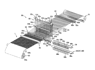
series by direct coupling. However, when tension is applied in the direction
of series connection, the spherical semiconductor elements receive this
tension directly, so that there is a danger of the spherical semiconductor
elements being torn away.
[0007] And in Patent Document #4 a flexible solar battery module is
disclosed, having a construction in which spherical semiconductor elements
in which pn junctions are formed are solidly pressed into a plurality of
meshes of a mesh like structural material (glass cloth) that is flat woven
using conducting lines made from glass fibers coated with silver as
horizontal strands and non conducting lines made from glass fiber as
vertical strands, and, along with electrodes being formed by application of
heat at high temperature in this state, also electrical connection of the
mesh like structural material and the spherical semiconductor elements is
simultaneously performed, and thereafter both sides of the mesh like
structure are laminated with resin film.
[0008] However, with the manufacturing method of Patent Document #4,
since the formation of the electrodes and establishment of the electrical
connections between the mesh like structural material and the spherical
semiconductor elements are performed simultaneously, accordingly there is
the problem that testing for checking the functioning of the spherical
semiconductor elements is not possible, because the pushing of the
spherical semiconductor elements into the meshes of the mesh like
3
CA 02808264 2013-02-12
structural material is not performed subsequently to formation of their
electrodes. For this reason, even if faulty spherical semiconductor elements
are mixed in with the others, this fact cannot be detected, and therefore the
defect ratio of the solar battery module becomes high.
[0009] Furthermore, with the finished solar battery module, since the
spherical semiconductor elements project on one of its surfaces, accordingly
light from the rear surface of the solar battery module cannot be effectively
utilized, and the light reception sensitivity for light that is incident from
the rear surface becomes low, which is undesirable. Moreover, since the
flexibility of the solar battery module when the module is mechanically
bent is not symmetrical between its two sides but is biased towards one
side, accordingly the convenience of use becomes bad.
[0010] Thus, with the manufacturing method of Patent Document #5, a
light-receiving module in sheet form or a light-emitting module in sheet
form that is transparent and flexible is manufactured by preparing a fabric
that is flat woven as a mesh like construction from horizontal strands made
from insulating filaments and vertical strands made from electrically
conductive filaments, by inserting a plurality of spherical semiconductor
elements that have a light-receiving function or a light-emitting function
and that have positive electrodes and negative electrodes into a plurality of
the net like meshes of the fabric in such a state that the polarities of their
electrodes are lined up, by connecting the elements in parallel in the
vertical direction (i.e. in the column direction) via pairs of conducting
lines,
and connecting them in series in the horizontal direction (i.e. in the row
direction by connecting between conducting lines in the row direction that
are adjacent with conducting lines for series connection, and by sealing the
resulting fabric within transparent resin sheets.
4
CA 02808264 2013-02-12
[0011] Since this light-receiving module or light-emitting module of
Patent Document #5 is a module in which the spherical semiconductor
elements are integrally installed in the fabric, accordingly it is a module
which has a double sided light reception or double sided light emission
characteristic and with which there is no bias towards either surface of the
light reception or light emission module, and thus a flexible module is
obtained both of whose sides have the same external appearance, and
which moreover can be bent in both directions in a symmetrical manner.
[0012] Patent Document #1: U.S. Patent No. 4,691,076
Patent Document #2: U.S. Patent No. 5,469,020
Patent Document #3: PCT Laid Open Publication W02004/001858
Patent Document #4: Japanese Laid Open Patent Publication Heisei 9
-16243
Patent Document #5: PCT Laid Open Publication W02005/041312
SUMMARY OF THE INVENTION
PROBLEMS TO BE SOLVED BY THE INVENTION
[0013] Now, when manufacturing the module of Patent Document #5
described above, in order to insert the plurality of spherical semiconductor
elements into the net meshes of the fabric that is woven in advance, and in
order to connect the positive and negative electrodes at the two ends of the
spherical semiconductor elements and the vertical strands that consist of
conducting lines together electrically with electrically conductive paste, it
is
necessary to keep the diameters of the semiconductor elements and the
gaps in the mesh fixed.
[0014] However, when performing the task described above of inserting
the spherical semiconductor elements into the meshes of the fabric which
are kept in the dilated state, there is a danger that, during the work, the
5
CA 02808264 2013-02-12
dimensions or the shape of the fabric will slump due to its own weight or
the like, so that the spaces between the horizontal strands or between the
vertical strands become too narrow and the spherical semiconductor
elements become blocked in the meshes; and also, conversely to the above,
there is a danger that a state will arise in which the spaces between the
horizontal strands or between the vertical strands become too great, so that
it is not possible to connect the positive and negative electrodes of the
spherical semiconductor elements to the vertical strands with electrically
conductive paste in an appropriate manner.
[0015] Moreover, with the structure of the module of Patent Document #5,
a pair of vertical strands are provided for each column, and a constant gap
is left between the vertical strand for the positive electrodes of each column
and the vertical strand for the negative electrodes of the adjacent column,
so that the structure is modularized. Due to this, in order to establish
series
connection between the plurality of spherical semiconductor elements in
each column and the plurality of semiconductor elements in adjacent
column, it is necessary to connect the end portions of the vertical strands in
the length direction together via conducting lines for series connection. In
other words, since it is necessary to provide conducting lines for series
connection, which are additional separate members exterior to the modules,
accordingly the number of components is increased, and considerable labor
is required for the work of wiring and so on, so that the manufacturing cost
is increased. Furthermore, there is a fear that the tensile strength and the
bending strength will become low, due to the provision of unnecessary
spaces between the columns.
[0016] Now, with a solar battery, a solar module, a solar panel or the like,
there are some aspects that cannot be satisfied only by power generation
6
CA 02808264 2013-02-12
efficiency and convenience of use of the product, or by durability and
economy thereof. For example, with a light reception device that supplies
electrical energy by receiving light from the exterior, or with a light
emission device that converts electrical energy into light which it emits to
the exterior, depending upon the application, there may be some factors in
relation to the human interface that relate to human sensitivities
[0017] When a solar battery is used by being attached to an electronic
device that is visible to the public, or to a building, a train carriage or
passenger car, clothes or personal equipment, then its presence exerts a
great influence on the external appearance. Due to this, in some cases there
is a requirement for some specific type of shape or characteristic
corresponding to the application; for example, there may be a requirement
for thinness, lightness, flexibility, optical transparency or see-through
characteristic, or the like. Furthermore, apart from physical factors, it is
desirable for the freedom in design, i.e. for the design aspects of coloration
and handling pattern, to be high.
[0018] Objects of the present invention are: to provide a method for
manufacturing a woven mesh substrate with semiconductor elements to
which a plurality of spherical semiconductor elements are installed during
the weaving of that woven mesh substrate using a weaving machine, the
method being capable of manufacturing a woven mesh substrate with
semiconductor elements of stabilized quality, and to provide a device for
manufacturing such a substrate; to provide a woven mesh substrate with
semiconductor elements in which spherical semiconductor elements having
a light-receiving function or a light-emitting function are installed on the
woven mesh substrate, with electrodes thereof being connected to
conducting lines; to provide a woven mesh substrate with semiconductor
7
CA 02808264 2013-02-12
elements that serves as an intermediate material that is capable of being
employed for various applications; to provide a woven mesh substrate with
semiconductor elements with which freedom of design can be enhanced; to
provide a woven mesh substrate with semiconductor elements with which
tensile strength and bending resistance can be enhanced.
MEANS TO SOLVE THE PROBLEMS
[0019] The method for manufacturing a woven mesh substrate with
semiconductor elements according to the present invention is a method for
manufacturing a woven mesh substrate with attached semiconductor
elements, in which a plurality of spherical semiconductor elements having
a light-receiving function or a light-emitting function, and each having a
first and a second electrode, are installed to a woven mesh substrate in net
form that is woven from a plurality of vertical strands that are insulating
and a plurality of horizontal strands that are electrically conductive,
characterized by comprising: a first step of shifting, with a heddle
mechanism, a first group of vertical strands including a plurality of vertical
strands arranged mutually parallel with fixed gaps between them, and a
second group of vertical strands including a plurality of vertical strands
positioned parallel to the first group of vertical strands and alternatingly
therewith, and creating a gap between the first and second groups of
vertical strands; a second step of supplying, with a shuttle mechanism, a
horizontal strand through the gap between the first and second groups of
vertical strands; a third step of pushing, with a reed mechanism, the
horizontal strand that has been supplied by the second process; a fourth
step of applying conductive junction blobs at a plurality of sites
corresponding to all or a part of the net meshes on the horizontal strand
that has been reed pushed by the third step; a fifth step of installing a
8
CA 02808264 2013-02-12
plurality of spherical semiconductor elements corresponding to all or a
portion of the plurality of sites at which the conductive junction blobs have
been applied by the fourth step, thus connecting a plurality of their first
electrodes or of their second electrodes to the horizontal strand; and a sixth
step of repeating the first step through the fifth step a plurality of times.
[0020] The device for manufacturing a woven mesh substrate with
semiconductor elements according to the present invention is a device for
manufacturing a woven mesh substrate with attached semiconductor
elements in which a plurality of spherical semiconductor elements having a
light-receiving function or a light-emitting function, and moreover each
having a first and a second electrode, are installed to a woven mesh
substrate in net form that is woven from a plurality of vertical strands that
are insulating and a plurality of horizontal strands that are electrically
conductive, characterized by comprising: a supply side guide roller that
guides a plurality of vertical strands supplied from a vertical strand supply
source; a heddle mechanism that shifts a first group of vertical strands
including a plurality of vertical strands arranged mutually parallel with
fixed gaps between them, and a second group of vertical strands including a
plurality of vertical strands positioned parallel to the first group of
vertical
strands and alternatingly therewith, and creates a gap between the first
and second groups of vertical strands; a shuttle mechanism that supplies a
horizontal strand through the gap created by the heddle mechanism
between the first and second groups of vertical strands; a reed mechanism
that pushes the horizontal strand that has been supplied by the shuttle
mechanism; an application mechanism that applies conductive junction
blobs at a plurality of sites on the horizontal strand corresponding to all or
a part of the net meshes; and a semiconductor element supply mechanism
9
CA 02808264 2013-02-12
that installs a plurality of spherical semiconductor elements to correspond
to all or a portion of the plurality of sites at which the conductive junction
blobs have been applied, and that thus connects the plurality of first
electrodes or of second electrodes to the horizontal strand.
[0021] Moreover, the woven mesh substrate with attached semiconductor
elements according to the present invention is a woven mesh substrate with
semiconductor elements, to which a plurality of spherical semiconductor
elements having a light-receiving function or a light-emitting function are
installed, characterized by comprising: a woven mesh substrate in net form,
woven from a plurality of vertical strands that are insulating and a
plurality of horizontal strands that are electrically conductive, and having
meshes arranged in a plurality of rows and a plurality of columns; and a
plurality of spherical semiconductor elements each of which has a light
-receiving function or a light-emitting function and a first and a second
electrode, and installed to a plurality of the meshes of the woven mesh
substrate in a state in which their conductive directions as specified by the
first and second electrodes are lined up in the vertical direction parallel to
the vertical strands; and in that: the plurality of spherical semiconductor
elements are grouped into a plurality of groups, taking row direction
element groups comprising a plurality of spherical semiconductor elements
lined up along the horizontal direction as units; the plurality of row
direction element groups are arranged in the plurality of rows, with
conductive connection members comprising one or a plurality of horizontal
strands being disposed between adjacent row direction element groups; the
plurality of spherical semiconductor elements of each row direction element
group are electrically connected in parallel via a pair of the conductive
connection members; and the plurality of row direction element groups are
CA 02808264 2013-02-12
connected in series via a plurality of the conductive connection members.
ADVANTAGES OF THE INVENTION
[0022] Since, according to the manufacturing method, while weaving the
woven mesh substrate from the plurality of vertical strands that are
insulating and the plurality of horizontal strands that are electrically
conductive using a weaving machine, the plurality of spherical
semiconductor elements are installed to that woven mesh substrate, and
their first and second electrodes are electrically connected to the horizontal
strands with the conductive junction blobs, accordingly when
manufacturing the woven mesh substrate, and when installing the
spherical semiconductor elements, it is possible to automate the application
of the conductive junction blobs, so that it is possible to manufacture a
woven mesh substrate with semiconductor elements of stabilized quality
efficiently with a small number of steps, and it is also possible to reduce
the
cost of manufacturing the woven mesh substrate with semiconductor
elements.
[0023] And, according to the manufacturing device, apart from
fundamentally obtaining similar advantageous effects described above, the
following further beneficial effects are also obtained. Since it is possible
to
additionally provide an application mechanism and a semiconductor
element supply mechanism while taking effective advantage of a supply
side guidance roller, a heddle mechanism, and a reed mechanism of an
already existing weaving machine, accordingly this is advantageous from
the point of view of design, manufacture, and manufacturing cost of a
manufacturing device for a woven mesh substrate with attached
semiconductor elements, and it is possible to produce a manufacturing
device for automatically manufacturing a woven mesh substrate with
11
CA 02808264 2015-04-23
attached semiconductor elements.
[0024] And since with this woven mesh substrate with attached
semiconductor elements, along with the plurality of spherical
semiconductor elements being grouped into a plurality of groups by taking
row direction element groups that consist of a plurality of spherical
semiconductor elements arranged along the horizontal direction as units,
and the plurality of row direction element groups being arranged in a
plurality of rows, also the conductive connection members that consist of
one or a plurality of horizontal strands are disposed between adjacent ones
of the row direction element groups, and the plurality of spherical
semiconductor elements in each of the row direction element groups are
electrically connected in parallel via a pair of the conductive connection
members, and the plurality of row direction element groups are connected
in series via the plurality of conductive connection members, accordingly, in
the case of a woven mesh substrate with attached semiconductor elements
for light reception, it is possible to set the voltage of the electricity that
is
generated freely via the number of series connections, and also it is possible
to set the current of the electricity that is generated freely via the number
of parallel connections.
[0025] And since, in the case of a woven mesh substrate with
semiconductor elements for light reception, the plurality of spherical
semiconductor elements are connected in series in the vertical direction and
also are connected in parallel in the horizontal direction, accordingly, even
if it happens that some portion becomes partially shaded, it is possible to
ensure that the influence that is exerted on the output of the other portion
of the spherical semiconductor elements that is not shaded is still kept to
the minimum limit.
12
CA 02808264 2013-02-12
Moreover, this woven mesh substrate with semiconductor elements
is capable of light reception or light emission with equal efficiency from
both its sides, both top and bottom. This woven mesh substrate with
semiconductor elements is an intermediate manufactured product that is
flexible, light in weight, thin, bendable, see through, and translucent to
daylight, and it can be finished into various types of final manufactured
product, according to the application.
[0026] Furthermore, since it is not necessary to provide any separate
conducting lines for series connection to the series connection construction
of this woven mesh substrate with semiconductor elements, accordingly it
is possible to reduce the number of components, so that it is possible to
reduce the manufacturing cost. And, since it is possible to arrange the
spherical semiconductor elements more closely together without providing
any unnecessary gaps between the element groups, accordingly it is
possible to enhance the tensile strength and the bending strength
(resistence), while also being able to enhance the light reception
performance or the light emission performance.
[0027] In addition to aaaabove described manufacturing method, it would
also be acceptable to arrange to employ various additional steps of the
following types.
(a) The transition to the third step may occur after having repeated
the first step and the second step at least twice in succession.
(b) After the fifth step and before the sixth step, there may be
provided a heat application step of applying heat to the conductive junction
blobs.
[0028] (c) After the fifth step and before the sixth step, there may be
provided a pulling out step of pulling out the woven mesh substrate with
13
CA 02808264 2013-02-12
attached semiconductor elements by a predetermined length.
(d) After the fifth step and before the sixth step, there may be
provided a covering step of covering both sides of the woven mesh substrate
with attached semiconductor elements with protective insulating layers
that are flexible and optically transparent.
[0029] (e) After the fifth step and before the sixth step, there may be
provided an overlaying step of overlaying both sides of the woven mesh
substrate with attached semiconductor elements with sheets of a synthetic
resin material that are flexible and optically transparent, and then
applying heat and pressure thereto.
[0030] (f) In the fourth step, first conductive junction blobs may be applied
at a plurality of sites on the horizontal strand at which the plurality of
spherical semiconductor elements are to be connected; in the fifth step, a
plurality of spherical semiconductor elements may be installed
corresponding to the plurality of sites at which the first conductive junction
blobs have been applied, with the plurality of first electrodes thereof being
connected to the plurality of sites; and, after the fifth step and before the
sixth step, there may be provided an application step of applying second
conductive junction blobs to the plurality of second electrodes of the
plurality of spherical semiconductor elements.
[0031] (g) In the fourth step, a plurality of conductive junction blobs may
be applied from the upper side of the horizontal strand; and, in the fifth
step, a plurality of spherical semiconductor elements may be installed from
the upper sides of the plurality of conductive junction blobs that were
applied in the fourth step.
[0032] And, in addition to above described manufacturing device, it would
also be acceptable to arrange to employ various additional elements or
14
CA 02808264 2013-02-12
members of the following types.
(h) The application mechanism may comprise a first rotation drum
and a plurality of L shaped dispensers that are fixed to the outer
circumferential surface of the first rotation drum at fixed intervals along
its
axial direction, and that are adapted to pick up and distribute conductive
junction blobs at their end portions.
[0033] (i) The semiconductor element supply mechanism may comprise a
second rotation drum to the interior of which negative pressure can be
supplied, and a plurality of air pincers that are made as L shaped pipe
members, and that are fixed to the outer circumferential surface of this
second rotation drum at fixed intervals along its axial direction.
(j) There may be provided a heat application mechanism that
applies heat to and dries the conductive junction blobs.
[0034] (k) There may be provided a pulling out mechanism that pulls out
the woven mesh substrate with semiconductor elements by successive
predetermined lengths.
(1) There may be provided a protective layer covering mechanism
that covers both sides of the woven mesh substrate with semiconductor
elements with flexible and optically transparent protective insulating
layers.
[0035] (m) There may be provided a heat application and pressurization
mechanism that forms a woven mesh substrate with semiconductor
elements sheet by applying heat and pressure to both sides of the woven
mesh substrate with semiconductor elements, in the state in which they are
overlaid with flexible and optically transparent sheets of synthetic resin
material.
[0036] Moreover, in addition to above described woven mesh substrate
CA 02808264 2013-02-12
with semiconductor elements, it would also be acceptable to arrange to
employ various additional constitutions of the following types.
(n) Each of the conductive connection members may consist of a first
and a second horizontal strand that are adjacent in the vertical direction so
as to contact one another and are electrically connected together, each of
which is woven in a zigzag state so as to contact front surfaces and rear
surfaces of the plurality of vertical strands alternatingly; and the weaving
pattern may sandwich the vertical strands by the first horizontal strands
and the second horizontal strands from their front surfaces and their rear
surfaces.
[0037] (o) First fabric portions of predetermined width in fabric form may
be formed at both end portions of the woven mesh substrate in the
lengthwise direction of the vertical strands by a plurality of horizontal
strands that are arranged more tightly than in the meshes, and by the
plurality of vertical strands; and second fabric portions of predetermined
width in fabric form may be formed at both side portions of the woven mesh
substrate in the lengthwise direction of the horizontal strands by a
plurality of vertical strands that are arranged more tightly than in the
meshes, and by the plurality of horizontal strands.
[0038] (p) Both sides of the woven mesh substrate and the plurality of
spherical semiconductor elements may be covered over by protective
insulating layers that are flexible and optically transparent.
(q) The woven mesh substrate and the plurality of spherical
semiconductor elements may be sealed in an embedded manner within
sheets of synthetic resin material that are flexible and optically
transparent, and synthetic resin film layers that are flexible and optically
transparent may be formed on both sides of the synthetic resin material
16
CA 02808264 2013-02-12
sheets.
[0039] (r) The vertical strands may be made as bundles of glass fibers or
synthetic resin fibers, and the horizontal strands may be made as
conducting lines in which thin metallic wires are covered in the form of coils
over the surfaces of bundles of glass fibers or synthetic resin fibers.
(s) The horizontal strands may be made as conducting lines
consisting of bundles of electrically conductive carbon fibers, or as
conducting lines in which thin metallic wires are covered in the form of coils
over the surfaces of' bundles of the carbon fibers.
[0040] (t) At least one insulating separation band of predetermined width,
in which a plurality of insulating lines are arranged in the horizontal
direction more tightly than in the meshes, may be formed at an
intermediate portion of the woven mesh substrate in the vertical direction.
BRIEF DESCRIPTION OF THE DRAWINGS
[0041] Fig. 1 is a plan view of a woven mesh substrate with attached
semiconductor elements according to a first embodiment of the present
invention;
Fig. 2 is a sectional view taken along lines II-II of Fig. 1;
Fig. 3 is an enlarged plan view of essential portions of the woven
mesh substrate with semiconductor elements;
Fig. 4 is a sectional view of a spherical solar cell;
Fig. 5 is an enlarged perspective view of a portion of a conducting
line;
Fig. 6 is an enlarged perspective view of a portion of an insulating
line;
Fig. 7 is a perspective view of a device for manufacturing the woven
mesh substrate with semiconductor elements;
17
CA 02808264 2013-02-12
Fig. 8 is an enlarged sectional view of principal portions of an
application mechanism and of a semiconductor element supply mechanism
of the device for manufacturing a woven mesh substrate with
semiconductor elements;
Fig. 9 is a plan view of a woven mesh substrate with semiconductor
elements according to a second embodiment of the present invention;
Fig. 10 is a sectional view taken along lines X-X of Fig. 9;
Fig. 11 is a perspective view of a device for manufacturing a woven
mesh substrate with semiconductor elements;
Fig. 12 is an enlarged sectional view of essential portions of an
application mechanism and a semiconductor element supply mechanism of
the device for manufacturing a woven mesh substrate with semiconductor
elements;
Fig. 13 is a perspective view of a device for manufacturing a woven
substrate according to a third embodiment of the present invention;
Fig. 14 is an enlarged perspective view of essential portions of the
device for manufacturing a woven mesh substrate;
Fig. 15 is an enlarged sectional view of essential portions of an
application mechanism and a semiconductor element supply mechanism of
the device for manufacturing a woven mesh substrate with semiconductor
elements;
Fig. 16 is an enlarged sectional view of essential portions of an
application mechanism and a semiconductor element supply mechanism of
the device for manufacturing a woven mesh substrate with semiconductor
elements;
Fig. 17 is a plan view of a woven mesh substrate with
semiconductor elements according to a fourth embodiment of the present
18
CA 02808264 2013-02-12
invention;
Fig. 18 is a perspective view of essential portions of the woven mesh
substrate with semiconductor elements;
Fig. 19 is an enlarged plan view of essntail portions of the woven
mesh substrate with semiconductor elements;
Fig. 20 is a sectional view of a spherical LED cell according to
another variant embodiment;
Fig. 21 is an enlarged plan view of essential portions of a woven
mesh substrate with semiconductor elements according to another variant
embodiment;
Fig. 22 is an enlarged plan view of principal portions of a woven
mesh substrate with semiconductor elements according to another variant
embodiment;
Fig. 23 is a plan view of a woven mesh substrate with
semiconductor elements according to another variant embodiment; and
Fig. 24 is a plan view of a woven mesh substrate with
semiconductor elements according to another variant embodiment.
BEST MODE FOR IMPLEMENTING THE INVENTION
[0042] In the following, the best mode for implementing the present
invention will be explained on the basis of embodiments for implementation
thereof.
EMBODIMENT 1
[0043] First, the woven mesh substrate with semiconductor elements 1 of
the present invention will be explained.
As shown in Figs. 1 through 3, the woven mesh substrate with
semiconductor elements 1 (hereinafter termed the "woven mesh substrate
with elements 1") comprises: a woven mesh substrate 2 that is formed as a
19
CA 02808264 2013-02-12
net having meshes 23 in matrix form arranged in a plurality of rows and a
plurality of columns, and woven from a plurality of vertical strands 21 that
are insulating and a plurality of horizontal strands 22 that are conductive;
a plurality of spherical solar cells 3 (which correspond to spherical
semiconductor elements) that are installed to the plurality of meshes 23 of
the woven mesh substrate 2; and a plurality of first and second conducting
junction materials 4, 5 for connecting these spherical solar cells 3 to the
horizontal strands 22 (i.e. to conductive connection members 20). Protective
insulating layers 6 are formed on both the sides of the woven mesh
substrate 2 and the plurality of spherical solar cells 3. It should be
understood that up, down, left, and right in Fig. 1 will be explained as being
up, down, left, and right.
[0044] With the manufacturing method and the manufacturing device 50
described hereinafter, this woven mesh substrate with elements 1 can be
woven continuously in the shape of a long belt. The woven mesh substrate
with elements 1 can be manufactured while setting the number of spherical
solar cells that are installed to the woven mesh substrate 2 and their
pattern of arrangement and their size and so on appropriately, according to
specification.
[0045] This woven mesh substrate with attached elements 1 is flexible,
and its optical transmission capability (i.e. its optical transmittivity) can
be
adjusted by adjusting the ratio of the number of meshes 23 to which the
plurality of spherical solar cells 3 are installed to the number of meshes 23
to which they are not installed. With the woven mesh substrate with
elements 1 of Fig. 1, a spherical solar cell 3 is installed to every second
location along each row in the left and right direction of the meshes 23, and
a spherical solar cell 3 is installed to every second location along each
CA 02808264 2013-02-12
column in the up and down direction of the meshes 23.
[0046] Next, the woven mesh substrate 2 will be explained.
As shown in Figs. 1 through 3, the woven mesh substrate 2
comprises the plurality of mutually parallel vertical strands 21 that extend
in the column direction (the vertical direction in Fig. 1), the plurality of
horizontal strands 22 that extend in the row direction (the horizontal
direction in Fig. 1) and that are woven between the plurality of vertical
strands 21 so as to be orthogonal to the plurality of vertical strands 21, and
the meshes 23 in a plurality of rows and columns that are surrounded by
this plurality of vertical strands 21 and this plurality of horizontal strands
22; and thus the woven mesh substrate 2, to which the spherical solar cells
3 can be installed, is defined by this plurality of vertical strands 21 and
this
plurality of horizontal strands 22. Each of the meshes 23 is formed in a
square shape as seen in plan view, with the length of each of its sides being
set to around 1.8 mm, which is approximately the same as the diameter of
the solar cells 3.
[0047] As shown in Figs. 1 and 2, a margin portion 24 which is woven
without installing any spherical solar cells 3 thereto is formed around the
exterior portion of this woven mesh substrate 2. This margin portion 24 is
formed from first fabric portions 25 of predetermined width that are defined
in fabric form, at both end portions of the vertical strands 21 in their
length
direction, by a plurality of the horizontal strands 22 that are arranged as a
tighter net than in the mesh 23 and by the plurality of vertical strands 21,
and from second fabric portions 26 of predetermined width that are defined
in fabric form, at both end portions of the horizontal strands 22 in their
length direction, by a plurality of the vertical strands 21 that are arranged
as a tighter net than in the mesh 23 and by the plurality of horizontal
21
CA 02808264 2013-02-12
strands 22. In these first fabric portions 25 the gaps between adjacent ones
of the horizontal strands 2q2 are around 1/3 of the mesh width, and
similarly in the second fabric portions 26 the gaps between adjacent ones of
the vertical strands 21 are around 1/3 of the mesh width.
[0048] Since the density of weaving of the vertical strands 21 or of the
horizontal strands 22 is higher in this margin portion 24, accordingly the
tensile strength and the bending strength are enhanced, and the durability
of the woven mesh substrate 2 also becomes higher. Moreover, if the woven
mesh substrate 2 is being manufactured in the shape of a long belt, then, by
providing the two first fabric portions 25 successively at predetermined
locations, it is possible, when this fabric is to be cut to a required length,
to
perform the cutting according to the shape in which the margin portion 24
is provided; and it is also possible for the solar cells 3 to be protected by
the
margin portion 24 during handling of the woven mesh substrate 2 after it
has been cut.
[0049] Next, the vertical strands 21 will be explained.
As shown in Fig. 6, the vertical strands 21 are made from, for
example, glass fiber or a synthetic resin fiber (for example polyester,
aramid, polyethylene, a liquid crystal polymer, or the like). In this
embodiment, the vertical strands 21 are made as lines including a plurality
of glass fibers (of diameter, for example, around 0.3 mm) bundled or twisted
together. It should be understood that, by employing glass fiber for the
vertical strands 21 and the horizontal strands 22, it is possible to obtain
vertical strands 21 and horizontal strands 22 whose mechanical strength is
high and whose heat resistance is excellent.
[0050] Next, the horizontal strands 22 will be explained.
As shown in Fig. 5, each of the horizontal strands 22 is made by
22
CA 02808264 2013-02-12
forming a bundle of, for example, glass fibers or synthetic resin fibers (for
example polyester, aramid, polyethylene, a liquid crystal polymer, or the
like) as a core fibers 22a, and by winding thin metallic wires 22b of copper
or the like thereon in the form of coils. In this embodiment, the horizontal
strands 22 are made by covering the surface of the core fibers 22a that
consists of a plurality of glass fibers (of diameter, for example, around 0.5
mm) with two thin metallic wires 22b of diameter 0.05 mm (for example
thin wires of copper) whose surfaces are plated with silver, in the form of
two coils. The two thin metallic wires 22b are wound left and right, so that
they cross one another. Since these horizontal strands 22 are made by
winding the two thin metallic wires 22b in the form of coils, accordingly
they can be bent to and fro in any direction, and moreover they have high
durability even if they are bent repeatedly to and fro. It should be
understood that the number of thin metallic wires 22 is not limited to being
two; as the covering, it would also be acceptable to use a plurality of more
than two thin metallic wires formed as coils.
[0051] Next, the spherical solar cells 3 will be explained.
As shown in Fig. 3, the plurality of spherical solar cells 3
(hereinafter termed "solar cells 3") have a light-receiving function (i.e.
they
are capable of generating electricity), and each comprises a positive
electrode 31 (i.e. a second electrode) and a negative electrode 32 (i.e. a
first
electrode) and is attached in one of the plurality of meshes 23 of the woven
mesh substrate 2, so that their conductive directions specified by their
positive electrodes 31 and negative electrodes 32 are lined up along the
direction parallel to the vertical strands 21. The vertical strands 21 are
positioned on both sides of the solar cells 3 in the row direction, i.e. on
their
left and right sides, and the horizontal strands 22 are positioned on both
23
CA 02808264 2013-02-12
sides of the solar cells 3 in the column direction, i.e. above and below them.
[0052] As shown in Fig. 4, each of the solar cells 3 includes: a p type
spherical semiconductor 33; a flat surface 34 formed on a portion of the
surface of the spherical semiconductor 33; a pn junction 36 shaped as a
spherical surface that is made by forming an n type diffused layer 35 on an
outer layer portion of the spherical semiconductor 33; an electrode pair
consisting of a positive electrode 31 (i.e. a second electrode) and a negative
electrode 32 (i.e. a first electrode) that are fixed so as to oppose one
another
across the center of the spherical semiconductor 33, and that are
electrically connected to the two sides of the pn junction 36; and a
reflection
prevention layer 37 that is formed over all portions of the structure other
than the positive electrode 31 and the negative electrode 32.
[0053] Now, a method for manufacturing these solar cells 3 will be
explained in a simple manner.
First, a small spherical p type silicon crystal (i.e. the spherical
semiconductor 33) is prepared, having diameter of from around 1.0 mm to
around 2.0 mm (in this embodiment 1.8 mm). In order to manufacture this
p type silicon crystal, for example, a small lump of p type silicon crystal is
melted, and the resulting liquid drop is allowed to cool and solidify while it
is kept as spherical as possible by surface tension. It should be understood
that the spherical silicon semiconductor crystal may be a single crystal, or
may be a polycrystal.
[0054] Next, a portion of this spherical silicon crystal is cut away to
provide the flat surface 34, and an Si02 layer is formed as a diffusion mask
on the surface of this flat surface 34 and around a portion surrounding it.
Thereafter, the pn junction 36 that is formed as a spherical surface is made
by diffusing an n type impurity inward from the outer layer portion of the p
24
CA 02808264 2013-02-12
type silicon crystal to a depth of around 0.5 pm to around 1.0 pm, with the
exception of the portion that has been masked by this Si02 layer, so that
this portion is converted into the n type diffused layer 35.
[0055] Next, after this impurity diffusion, the oxide layer is eliminated as
far as possible, and the reflection prevention layer 37 is made by
sequentially forming layers of Si02 and Si3N4 over the entire surface. And
next a conductive paste, whose principal components are glass frit and
silver, is printed on the flat surface 34 described above in the form of a
dot,
and moreover a conductive paste including glass frit, aluminum, and silver
is printed in the form of a dot on the summit surface of the n type diffused
layer 35, opposite to the flat surface 34 and with the center of the spherical
semiconductor 33 between them.
[0056] And heat is applied at 800 C for a short time period (around one to
two minutes) in an atmosphere of inert gas. Due to this processing, the
electrode members that include glass frit pierce through the reflection
prevention layer 37, and thereby the positive electrode 31 and the negative
electrode 32 are formed to be in ohmic contact with the p type
semiconductor surface and the n type semiconductor surface. The plurality
of spherical solar cells 3 are manufactured in this manner.
[0057] This spherical solar cell 3 is an element having the following
characteristics.
First, the spherical crystal is formed by taking advantage of the
surface tension of the silicon crystal material, and it will be sufficient
only
to use a small amount of silicon raw material, since the spherical solar cell
3 can be manufactured with low grinding processing loss. Moreover, since
the positive electrode 31 and the negative electrode 32 are provided in the
form of dots so as to oppose one another along the center line of the
CA 02808264 2013-02-12
spherical silicon crystal, accordingly light from almost all directions can be
received and generates electricity, except for light from directly above the
axial line that connects the two electrodes. Thus not only is the same
general level of output received even if the direction of incidence of the
light
changes, but, apart from this, it is also possible to receive both reflected
light and scattered light at the same time, so that the light reception
characteristic is more excellent than that of a planar light reception type
solar cell. As a result, high output is obtained.
[0058] Next, the first and second conductive junction materials 4, 5 will be
explained. As shown in Fig. 3, each of the plurality of first conductive
junction material 4 is connected between the negative electrode 32 of one of
the solar cells 3 and one of the horizontal strands 22, while each of the
plurality of second conductive junction material 5 is connected between the
positive electrode 31 of one of the solar cells 3 and one of the horizontal
strands 22. The conductive junction materials 4, 5 are made from a silver
paste (one in which silver powder is mixed into epoxy resin). When
connecting the solar cells 3 and the horizontal strands 22 (i.e. the
conductive connection members 20) together with this silver paste, for
example, after having applied the silver paste to the junction sites between
the positive electrodes 31 and the horizontal strands 22 and to the junction
sites between the negative electrodes 32 and the horizontal strands 22, the
silver paste is hardened by application of heat using a heat application
mechanism 61 that will be described hereinafter and is thus dried, and
thereby it is possible to connect the positive electrodes 31 and the negative
electrodes 32 of the solar cells 3 to the horizontal strands 22 electrically,
and moreover to adhere them mechanically thereto.
[0059] Now, the series parallel connection construction (circuit) of the
26
CA 02808264 2013-02-12
plurality of solar cells 3 will be explained.
As shown in Figs. 1 through 3, the plurality of solar cells 3 are
grouped into a plurality of groups in which row direction element groups 3A
consisting of a plurality of the solar cells 3 arrayed along the horizontal
direction (i.e. along the row direction) may be taken as units, so that along
with this plurality of row direction element groups 3A being arranged in a
plurality of rows, conductive connection members 20 are disposed between
adjacent row direction element groups 3A. The conductive connection
member 20 consists of single horizontal strand 22. The plurality of solar
cells 3 in each of the row direction element groups 3A are electrically
connected in parallel via its corresponding pair of two conductive
connection members 20, and the plurality of row direction element groups
3A are connected in series via the plurality of conductive connection
members 20.
[0060] Since it is possible to connect the plurality of solar cells 3 of
adjacent row direction element groups 3A in series in this manner via the
conductive connection member 20 that consists of the single horizontal
strand 22, accordingly it is possible to arrange the plurality of row
direction
element groups 3A that are disposed in a plurality of rows in a state in
which they are closely contacted together with no gaps being present
between them in the column direction. Due to this, it is possible to
manufacture a woven mesh substrate with elements 1 on which a large
quantity of the solar cells 3 are installed, and it is thus possible to
enhance
the light-receiving performance of the woven mesh substrate with elements
1. It should be understood that, if the solar cells 3 are replaced by
light-emitting diodes, then it is possible to enhance the light- emitting
performance.
27
CA 02808264 2013-02-12
[0061] Next, the protective insulating layers 6 will be explained.
As shown in Figs. 1 and 2, these protective insulating layers 6 are
coatings that cover both the upper and lower sides of the woven mesh
substrate with elements 1 to a thickness of, for example, around 25 pm with
a surface coating made from, for example, a silane coupling compound, or
with a layer of parylene (product name, made by the Union Carbide
Chemicals and Plastics Co.) which is a para xylylene series polymer. These
protective insulating layers 6 are flexible and transparent to light. After
the
woven mesh substrate with elements 1 has been manufactured, protective
insulating layers 6 that are made from a silane coupling compound may be
formed as coatings according to a spray method by a protective layer
covering mechanism 62 that will be described hereinafter. It should be
understood that, after the woven mesh substrate with elements 1 has been
manufactured, protective insulating layers 6 that are made from parylene
may be formed as coatings at normal temperature according to a chemical
vapor deposition method by a parylene protective layer covering
mechanism not shown in the figures.
[0062] Since, in the interior of a solar battery module or of a solar cell
panel to which the woven mesh substrate with elements 1 is installed, the
solar cells 3 that can receive light three dimensionally can easily receive
direct sunlight and also light that has been reflected and scattered,
accordingly the efficiency of utilization of light incident from the exterior
is
high, and moreover a high stabilized output is obtained. In particular, the
reduction in output is small when the direction of incidence of direct
sunlight changes, or when the weather becomes overcast, and the total
amount of electricity that is generated becomes great as compared to the
case of a planar type solar battery module on which the light-receiving is
28
CA 02808264 2013-02-12
performed two dimensionally. Moreover, it is possible to make a woven
mesh substrate with elements which has excellent freedom in design by
employing colored insulating lines in the woven mesh substrate with
elements 1, by installing colored ornamental spheres of the same size as the
solar cells 3 in some of the meshes 23, and so on.
[0063] Furthermore, in order to connect the woven mesh substrate with
attached elements 1 electrically and mechanically to an external device, it
is possible to connect the plurality of horizontal strands 22 to integrated
terminals 45, 46 by connecting together the plurality of horizontal strands
22 at both the left and right end portions of the lower side first fabric
portion 25 with solder or silver paste, and by connecting together the
plurality of horizontal strands 22 at both the left and right end portions of
the upper side first fabric portion 25 with solder or silver paste. It is
possible to implement a woven mesh substrate with attached elements
having a larger output of electrical power by connecting an appropriate
number of the woven mesh substrates with elements 1 in parallel and/or in
series using such external terminals 45,46. It should be understood that it
would also be acceptable to combine and integrate together a plurality of
the horizontal strands 22 with solder or silver paste at a plurality of
locations on the upper and lower first fabric portions 25 along the
horizontal direction. In this case, since not only is the strength of the
first
fabric portions 25 enhanced but also the electrical current from the
plurality of solar cells 3 is outputted via the bundles of combined horizontal
strands 22 and from the external terminals 45, 46, accordingly it is possible
to alleviate the current load on the most inward ones of the horizontal
strands 22 of the first fabric portions 25, which are the ones that are
adjacent to the plurality of solar cells 3.
29
CA 02808264 2013-02-12
[0064] Since, in the woven mesh substrate with elements 1, the solar cells
3 are electrically and mechanically connected by being installed in the
meshes 23 that are surrounded by the vertical strands 21 and the
horizontal strands 22 that have the same structure as the fabric,
accordingly it is sufficient to employ a lower number of essential members,
and it is possible to reduce the cost of the material and of processing, so
that
it is possible to realize significant economy. Moreover, it is possible to
make
the woven mesh substrate with elements 1 thin and light, and it is possible
to endow it with a flexible construction which is also see through.
[0065] Next, a manufacturing device 50 for manufacturing the woven
mesh substrate with elements 1 will be explained.
As shown in Figs. 7 and 8, the manufacturing device 50 is able to
manufacture the woven mesh substrate with elements 1 while shifting the
resulting material from the upstream side towards the downstream side.
The manufacturing device 50 comprises a supply side guide roller 51 at the
farthest upstream side, a heddle mechanism 53, a shuttle mechanism 54, a
reed mechanism 55, an application mechanism 56 that functions as a first
application mechanism 57 and a second application mechanism 58, a
semiconductor element supply mechanism 59, a heat application
mechanism 61 (not shown in Fig. 7), a protective layer covering mechanism
62, a pulling out mechanism 63 at the farthest downstream side, and so on.
[0066] This manufacturing device 50 is a machine that manufactures a
woven mesh substrate with elements 1 in which a plurality of solar cells 3
that have the function of receiving light, and each of which moreover has a
positive electrode 31 and a negative electrode 32, are installed to a woven
mesh substrate that is woven in net form from a plurality of vertical
strands 21 that are insulating and a plurality of horizontal strands 22 that
CA 02808264 2013-02-12
are electrically conductive, and that has meshes 23 laid out in matrix form
in a plurality of rows and a plurality of columns. It should be understood
that, in Fig. 7, the margin portion 24 of the woven mesh substrate with
attached elements 1 is omitted.
[0067] Next, the supply side guide roller 51 will be explained.
As shown in Fig. 7, the supply side guide roller 51 is rotatably
supported on the frame of the manufacturing device 50, and is rotationally
driven by a roller drive mechanism (not shown). This supply side guide
roller 51 is a mechanism that guides a plurality of vertical strands 21 that
are supplied from a vertical strand supply source (not shown) towards the
heddle mechanism 53 in a well ordered state, while changing their
directions. While the plurality of vertical strands 21 are arranged with gaps
of around 1.8 mm between them in the axial direction of the supply side
guide roller 51, except for a number thereof that are positioned closely
together at the two side end portions of the plurality of vertical strands 21
(corresponding to the second fabric portions 26), this gap value is not to be
considered as being particularly limitative; it can be changed as
appropriate, according to the configuration for the woven mesh substrate
with elements 1. It should be understood that the gaps between the vertical
strands 21 in the portions that define the second fabric portions 26 of the
woven mesh substrate with elements 1 are around 0.6 mm, although this is
not shown in the figure.
[0068] A guide plate 52 is provided between the supply side guide roller 51
and the heddle mechanism 53 at its downstream side. This guide plate 52
has a pair of flat plate portions 52a, 52b and an opening portion 52c that is
defined between the pair of flat plate portions 52a, 52b and that extends in
the lengthwise direction orthogonal to the vertical strands 21. This guide
31
CA 02808264 2013-02-12
plate 52 divides the plurality of vertical strands 21 into two groups: a first
group of vertical strands 21a that pass over the upper side of the flat plate
portion 52a, pass through the opening portion 52c, and pass under the
under side of the flat plate portion 52b; and a second group of vertical
strands 21b that pass under the under side of the flat plate portion 52a,
pass through the opening portion 52c, and pass over the upper side of the
flat plate portion 52b. It should be understood that, in this embodiment, in
the plurality of vertical strands 21, the odd numbered vertical strands 21
from the right side edge in Fig. 7 are taken as being the first group of
vertical strands 21, while the even numbered vertical strands 21 are taken
as being the second group of vertical strands 21.
[0069] Next, the heddle mechanism 53 will be explained.
As shown in Fig. 7, the heddle mechanism 53 comprises first and
second heddle members 53a, 53b, and a reciprocating drive member 53c for
reciprocatingly shifting these first and second heddle members 53a, 53b
relatively up and down. This heddle mechanism 53 is a device that shifts up
and down the first group of vertical strands 21a including its plurality of
vertical strands 21 arranged in parallel with predetermined gaps between
them, and the second group of vertical strands 21b including its plurality of
vertical strands 21 that are parallel to the first group of vertical strands
21a and that are positioned alternatingly with them, thus forming a gap for
passing a shuttle 54a between the first and second groups of vertical
strands 21a, 21b.
[0070] Each of the first and second heddle members 53a, 53b comprises a
long and narrow plate shaped upper frame 53d, a lower frame 53e, and a
plurality of healds 53f that extend in the vertical direction and join the
upper frame 53d and lower frame 53e. Strand holes 53g are formed in the
32
CA 02808264 2013-02-12
central portions of the healds 53f for passing the vertical strands 21. The
heddle mechanism 53 is constructed so that the first and second heddle
members 53a, 53b are somewhat mutually deviated in the horizontal
direction (i.e. in the width direction of the woven mesh substrate with
elements 1), and so that the plurality of healds 53f of the second heddle
member 53b are positioned between the plurality of healds 53f of the first
heddle member 53a. Each of the plurality of vertical strands 21 of the first
group of vertical strands 21a is passed through one of the plurality of
strand holes 53g of the first heddle member 53a, and similarly each of the
plurality of vertical strands 21 of the second group of vertical strands 21b
is
passed through one of the plurality of strand holes 53g of the second heddle
member 53b. It should be understood that it would also be acceptable to
adopt a structure for the heddle mechanism 53 in which a pair of upper and
lower carrier rods are provided to the upper frame 53d and to the lower
frame 53e respectively, and the healds 53f are supported by these carrier
rods.
[0071] The reciprocating drive member 53c comprises a rotation shaft 53h
that extends in the direction orthogonal to the vertical strands 21, a pair of
pulley members 53i that are fixed to the two end portions of the shaft 53h, a
pair of belt members 53j that are engaged over these pulley members 53i
and are linked to the upper end portions of the first and second heddle
members 53a, 53b, a reciprocating rotation mechanism (not shown) that
rotates the rotation shaft 53h to and fro in a reciprocating manner, and so
on. Due to this reciprocating operation of the reciprocating drive member
53c, when the first heddle member 53a and the first group of vertical
strands 21a are shifted upwards, the second heddle member 53b and the
second group of vertical strands 21b shift relatively downwards; and, when
33
CA 02808264 2013-02-12
the first heddle member 53a and the first group of vertical strands 21a are
shifted downwards, the second heddle member 53b and the second group of
vertical strands 21b shift relatively upwards; and, in either case, a gap is
formed between the first and second groups of vertical strands 21a, 21b for
the shuttle member 54a to pass through. While this feature is omitted from
Fig. 7, it should be understood that, below the first and second heddle
members 53a, 53b, the reciprocating drive member 53c has a rotation shaft
that is rotated to and fro in a reciprocating manner by a reciprocating
rotation mechanism in the same way as the rotation shaft, a pair of pulley
members that are fixed to the two end portions of this rotation shaft in the
same way as the pair of pulley members 53i, a pair of belt members that are
engaged over these pulley members and are linked to the lower end
portions of the first and second heddle members 53a, 53b, and so on.
[0072] Next, the shuttle mechanism 54 will be explained.
As shown in Fig. 7, the shuttle mechanism 54 comprises a shuttle
member 54a to which the end portion of a horizontal strand 22 is attached,
a shuttle drive mechanism (not shown) that can drive the shuttle member
54a to reciprocate to and fro in the left and right direction, a horizontal
strand supply mechanism (not shown) that supplies the horizontal strand
22 to the shuttle member 54a, and so on. The horizontal strand 22 is
supplied by the shuttle member 54a into the wedge shaped gap created by
the heddle mechanism 53 between the first and second groups of vertical
strands 21a, 21b. In concrete terms, first, the shuttle member 54a is shifted
from the right side in Fig. 7 to the left side through the gap between the
first and second groups of vertical strands 21a, 21b, so that the horizontal
strand 22 is passed through in a state orthogonal to the first and second
groups of vertical strands 21a, 21b, and then the horizontal strand 22 is cut
34
CA 02808264 2013-02-12
off at both left and right sides, while leaving portions corresponding to the
second fabric portions 26.
[0073] Next, the reed mechanism 55 will be explained.
As shown in Figs. 7 and 8, the reed mechanism 55 comprises a plate
shaped member 55a that is oriented vertically and is elongated in the
horizontal direction, and a reed drive mechanism (not shown) that shifts
the plate shaped member 55a forwards and backwards through just a
predetermined stroke, and a plurality of vertically extending slits 55b are
formed at regular intervals in the plate shaped member 55a. The reed
mechanism 55 is a device that, using a guide, strikes the horizontal strands
22 that have been supplied by the shuttle mechanism 54 so as to push and
tamp them towards the downstream side, and that, along with regulating
the horizontal strands 22 into an orthogonal state with respect to the
vertical strands 21, also tightly packs the horizontal strands 22 against the
solar cells 3 on the downstream side. The plurality of vertical strands 21 of
the first group of vertical strands 21a pass through alternate ones of the
plurality of slits 55b, and the plurality of vertical strands 21 of the second
group of vertical strands 21b pass through the other alternate ones of the
slits 55b.
[0074] Next the application mechanism 56 will be explained, this being a
combination of the first application mechanism 57 and the second
application mechanism 58.
As shown in Figs. 7 and 8, the first application mechanism 57 is a
device that applies first conductive junction blobs 4 at a plurality of sites
on
the horizontal strands 22 that have been tamped by the reed, so as to
connect them to the plurality of negative electrodes 32 of the plurality of
solar cells 3. And, while the second application mechanism 58 is a device
CA 02808264 2013-02-12
that applies second conductive junction blobs 5 to the plurality of positive
electrodes 31 of the plurality of solar cells 3 that have been installed by
the
semiconductor element supply mechanism 59, in this embodiment, the first
and second application mechanisms 57,58 are constituted as a single
common application mechanism 56.
[0075] As shown in Fig. 8, the application mechanism 56 is disposed at the
downstream side of the reed mechanism 55, and is located below the woven
mesh substrate 2 that has been woven from the plurality of vertical strands
21 and the plurality of horizontal strands 22. However, in Fig. 7, this
mechanism is shown in a disassembled state.
The application mechanism 56 comprises a first rotation drum 56a
that is capable of being rotationally driven by just a predetermined angle
(around 270 ), and a plurality of L shaped dispensers 56b that are fixed to
the outer circumferential surface of the first rotation drum 56a at fixed
intervals along its axial direction. The plurality of dispensers 56b of this
embodiment are fixed at every second pitch, corresponding to the diameter
of the solar cells 3.
[0076] The first rotation drum 56a is rotatably supported on the frame of
the manufacturing device 50 (not shown), and is rotationally
reciprocatingly driven by a drum rotation drive mechanism (not shown). It
should be understood that the application mechanism 56 also includes a
reciprocating drive mechanism (not shown) that can shift the first rotation
drum 56a to and fro by just a predetermined small stroke in its axial
direction (for example, one pitch).
[0077] As shown in Fig. 8, the dispensers 56b are formed in L shapes.
Each of the dispensers 56b is made so as to be capable of picking up and
dispensing a conductive junction blob 4, 5 at its end portion. When the
36
CA 02808264 2013-02-12
plurality of dispensers 56b are to pick up the plurality of conductive
junction blobs 4, 5, in the state in which each of the dispensers 56b is in
its
pickup position, a plurality of the conductive junction blobs 4, 5 are
supplied to positions below the end portions of the dispensers 56b by a
supply mechanism 64 that can slide in the direction of the arrow sign in
Fig. 8, and each of the conductive junction blobs 4, 5 is then picked up at
the
end portion of one of the dispensers 56b by the first rotation drum 56a being
rotated slightly in the anticlockwise direction. It should be understood that,
for the dispensers 56b, it would also be acceptable to employ devices that
pick up the conductive junction blobs 4, 5 with air at negative pressure,
thus distributing the conductive junction blobs 4, 5 with negative
pressurized air.
[0078] Next, the semiconductor element supply mechanism 59 will be
explained. As shown in Fig. 8, the semiconductor element supply
mechanism 59 is disposed at the downstream side of the reed mechanism
55, and above the woven mesh substrate 2. However, in Fig. 7, this
mechanism 59 is shown in a disassembled state.
The semiconductor element supply mechanism 59 comprises a
second rotation drum 59a that can be driven by predetermined rotational
angles and to the interior of which negative pressure is supplied, and a
plurality of air pincettes 59b formed in L shapes that are fixed to the outer
circumferential surface of the second rotation drum 59a with fixed gaps
between them. The plurality of air pincettes 59b are fixed with intervals
between them that are approximately twice the diameter of the solar cells
3. The semiconductor element supply mechanism 59 is a device that, by
installing the plurality of solar cells 3 to the woven mesh substrate 2 so
that
they correspond to the plurality of locations on the horizontal strands 22 at
37
CA 02808264 2013-02-12
which the first conductive junction blobs 4 are applied, connects the
plurality of negative electrodes 32 at the respective plurality of locations
described above.
[0079] The second rotation drum 59a is supported on the frame not shown
in the figure of the manufacturing device 50 so that it can be rotationally
driven, and is reciprocatingly rotationally driven to and fro by a
reciprocating rotation drive mechanism (not shown). Negative pressure can
be introduced into the interior of the second rotation drum 59a by a
negative pressure generation mechanism not shown in the figures. This
second rotation drum 59a can be changed over to a holding position (shown
in Fig. 8 by the double dotted chain lines) in which it receives and holds a
solar cell 3 from an external supply mechanism, and to a loading position
(the position of the solar cell 3a at the rightmost side in Fig. 8) in which
it is
rotated by, for example, around 270 in the clockwise direction from the
holding position, and in which it joins the solar cell 3 to one of the first
conductive junction blobs 4. It should be understood that the semiconductor
element supply mechanism 59 operates together with the first rotation
drum 56a of the application mechanism 56, and also includes a
reciprocating drive mechanism (not shown) for shifting the second rotation
drum 59a to and fro by just a predetermined small stroke in its axial
direction (with one pitch being equal, for example, to the diameter of the
solar cells 3).
[0080] As shown in Fig. 8, the air pincettes 59b are made as L shaped pipe
members. Nozzles 59c are formed at the end portions of the air pincettes
59b, and these are connected to the interior of the second rotation drum 59a
via negative pressure conduction passages. When the solar cells 3 are to be
held by the air pincettes 59b, the solar cells 3 are supplied to the end
38
CA 02808264 2013-02-12
portions of the air pincettes 59b after having been positioned by a supply
mechanism (not shown) into a predetermined attitude (i.e., the attitude in
which the negative electrodes 32 are on top and the positive electrodes 31
are underneath); and, since negative pressure is generated at the nozzles
59c at the end portions of the air pincettes 59b when negative pressure is
introduced into the interior of the second rotation drum 59a, accordingly
their end portions pick up and hold the positive electrode 31 sides of the
solar cells 3 due to this negative pressure.
[0081] Next, the heat application mechanism 61 will be explained.
As shown in Fig. 8, the heat application mechanism 61 is disposed
in the neighborhood of the application mechanism 56 and the
semiconductor element supply mechanism 59. This heat application
mechanism 61 is a device that, after the solar cells 3 have been installed to
the woven mesh substrate 2, causes the conductive junction blobs 4, 5 at the
junction portions between the solar cells 3 and the horizontal strands 22 to
harden in a short period of time. In concrete terms, the heat application
mechanism 61 irradiates the conductive junction blobs 4, 5 locally with hot
air or infrared radiation, so that heat is applied to them and they are dried
and hardened.
[0082] Next, the protective layer covering mechanism 62 will be
explained. As shown in Figs. 7 and 8, the protective layer covering
mechanism 62 has a tunnel shaped passage aperture, and is disposed
downstream from the heat application mechanism 61. While the woven
mesh substrate with elements 1 is passing through the passage aperture,
both the upper and lower sides of the woven mesh substrate with elements
1 are covered by a spray method with protective insulating layers 6 that are
flexible and optically transparent (i.e. with surface coatings of a silane
39
CA 02808264 2013-02-12
coupling compound).
[0083] Next, the pulling out mechanism 63 will be explained.
As shown in Fig. 7, the pulling out mechanism 63 comprises a
winding up roller 63a that winds up the woven mesh substrate with
elements 1, a guide roller 63b that guides the woven mesh substrate with
elements 1 in the direction of the winding up roller 63a, and so on, and is
disposed at the furthest downstream side of the manufacturing device 50.
The winding up roller 63a is supported on the frame (not shown) of the
manufacturing device 50 so as to be capable of being rotationally driven,
and operates together with the other mechanisms such as the application
mechanism 56, the semiconductor element supply mechanism 59, and so
on, so as to wind up the woven mesh substrate with elements 1 onto the
winding up roller 63 with a pulling out drive mechanism (not shown), while
intermittently pulling it out one pitch at a time.
[0084] Next, the manufacturing method for manufacturing the woven
mesh substrate with elements 1 will be explained.
This manufacturing method is a method for manufacturing, with
the manufacturing device 50, a woven mesh substrate with elements 1 in
which a plurality of solar cells 3, having a function of light reception and
each having a positive electrode 31 and a negative electrode 32, are
installed on a woven mesh substrate 2 in net form that is woven from a
plurality of vertical strands 21 that are insulating and a plurality of
horizontal strands 22 that are electrically conductive, and having a mesh
23 in matrix form with a plurality of rows and a plurality of columns.
[0085] First, in a first step, after a plurality of vertical strands 21 have
been passed over the supply side guide roller 51 and through the guide
plate 52, they are divided by the heddle mechanism 53 into the first group
CA 02808264 2013-02-12
of vertical strands 21a including a plurality of the vertical strands 21 that
are arranged in parallel with fixed intervals between them, and the second
group of vertical strands 21b including a plurality of the vertical strands 21
that are arranged in parallel with the first group of vertical strands 21a
and are positioned alternatingly therewith. And the first group of vertical
strands 21a and the second group of vertical strands 21b are shifted up and
down by the heddle mechanism 53, so as to create gaps between the first
group of vertical strands 21a and the second group of vertical strands 21b
for the shuttle to pass through.
[0086] Next, in a second step, the shuttle member 54a of the shuttle
mechanism 54 is passed through the gap between the first and second
groups of vertical strands 21a, 21b in the direction orthogonal to the
vertical strands 21, so that a horizontal strand 22 is supplied. This one
horizontal strand 2 constitutes one conductive connection member 20.
[0087] Next, reed pushing is performed in a third step, and the horizontal
strand 22 that has been supplied in the second step is pushed to the
downstream side by the reed mechanism 54, so that the horizontal strand
22 is regulated into the state of extending orthogonally with respect to the
vertical strands 21. At this time, if a plurality of solar cells 3 were
supplied
at the downstream side in the processing one cycle before, then the
horizontal strand 22 is pushed against their positive electrodes 31. In this
manner, first, the woven mesh substrate in net form 2 woven from the
plurality of vertical strands 21 that are insulating and the plurality of
horizontal strands 22 that are electrically conductive is manufactured.
[0088] Next, in a fourth step, first conductive junction blobs 4 consisting of
silver paste are applied by the application mechanism 56 (i.e. by the first
application mechanism 57) at a plurality of sites on the horizontal strand
41
CA 02808264 2013-02-12
22 that has been pushed by the reed mechanism in the third step, so as to
connect the plurality of solar cells 3 there.
[0089] First, in concrete terms, first conductive junction blobs 4 that are
supplied by the supply mechanism 64 are picked up at the end portions of
the plurality of dispensers 56b that are in their pickup positions. Next, the
plurality of dispensers 56b are rotated by about 2700 in the anticlockwise
direction, so that the plurality of dispensers 56b are changed over to their
application positions and the first conductive junction blobs 4 are applied to
a plurality of sites on the horizontal strand 22. Thereafter, the plurality of
dispensers 56b are rotated by about 270 in the clockwise direction, so that
they are returned to their pickup positions.
[0090] Next, in a fifth step, a plurality of solar cells 3 are installed by
the
semiconductor element supply mechanism 59 so as to correspond to the
plurality of sites where the first conductive junction blobs 4 were applied in
the fourth step, and their plurality of negative electrodes 32 are joined to
the first conductive junction blobs 4 at the plurality of sites. The plurality
of
solar cells 3 that are supplied by this fifth step constitute one element
group 3A along the row direction.
[0091] In concrete terms, first, the solar cells 3 are supplied to the end
portions of the air pincettes 59b which are in their holding positions, and
the solar cells 3 are held by the air pincettes 59b due to the negative
pressure that is generated at the nozzles 59c. Next, the air pincettes 59b
are rotated by about 270 in the clockwise direction, so that the air
pincettes 59b are changed over to their loading positions, and the negative
electrodes 32 of the solar cells 3a are joined to the horizontal strand 22 to
which the first conductive junction blobs 4 have been applied. Thereafter,
the plurality of air pincettes 59b are returned to their holding positions by
42
CA 02808264 2013-02-12
being rotated by about 270 in the anticlockwise direction. At this time,
since the semiconductor element supply mechanism 59 pushes the solar
cells 3 in the downstream direction after having joined them to the first
conductive junction blobs 4, accordingly it is possible to anticipate the same
beneficial effect as that provided by the reed mechanism 55.
[0092] And, in a sixth step, the woven mesh substrate 2 is pulled outward
to the downstream side by the pulling out mechanism 63 by one pitch,
which corresponds to the diameter of the solar cells 3. This sixth step is one
corresponding to the pulling out step that is performed after the fifth step.
[0093] Next, in a seventh step, second conductive junction blobs 5
consisting of silver paste are applied by the application mechanism 56 (i.e.
by the second application mechanism 58) to the plurality of positive
electrodes 31 of the plurality of solar cells 3 that were installed by the
fifth
step. This seventh step is one corresponding to the application step.
[0094] In concrete terms, first the second conductive junction blobs 5 that
are supplied by the supply mechanism 64 are picked up at the end portions
of the plurality of dispensers 56b which are in their pickup positions. Next,
the plurality of dispensers 56b are rotated in the anticlockwise direction by
about 270 , so that the plurality of dispensers 56b are changed over to their
application positions, and the second conductive junction blobs 5 are
applied to the plurality of positive electrodes 31. Thereafter, the plurality
of
dispensers 56b are rotated in the clockwise direction by about 270 , so that
they are returned to their pickup positions.
[0095] During the return shifting of the plurality of dispensers 56b
described above, in order to install an amount of the plurality of solar cells
3 corresponding to one pitch to the woven mesh substrate 2 to create the
next line of the weave: the first group of vertical strands 21a and the second
43
CA 02808264 2013-02-12
group of vertical strands 21b are shifted by the heddle mechanism 53 so
that they come into the opposite up/down positional relationship from their
original up/down positional relationship (the first step); the shuttle member
54a is passed through the gap between the first and second groups of
vertical strands 21a, 21b so as to supply a horizontal strand 22 (the second
step); and the horizontal strand 22 that has been supplied is pushed by the
reed mechanism 55 (the third step). Thereafter the fourth through the fifth
steps are executed, and the plurality of conductive junction blobs 4 and the
plurality of solar cells 3 are supplied by the application mechanism 56 and
the semiconductor element supply mechanism 59.
[0096] Next in an eighth step, after the seventh step, the conductive
junction blobs 4, 5 in the row direction are irradiated with hot air or
infrared radiation or the like by the heat application mechanism 61 that is
disposed on the downstream side of the application mechanism 56 and the
semiconductor element supply mechanism 59, and the conductive junction
blobs 4, 5 are thereby dried, so that these conductive junction blobs 4,5 are
hardened over a short time period. Due to this, it is possible to join
together
the horizontal strands 22 and the plurality of solar cells 3 solidly, and to
connect them together electrically. It would be acceptable to employ any of
irradiation with laser light or infrared radiation, irradiation with a
condensing lamp, or local blowing of heated air as the method for
application of heat. This eighth step is one corresponding to the heat
application step.
[0097] Next in a ninth step, after the eighth step, while the woven mesh
substrate with elements 1 passes through the tunnel shaped passage
aperture of the protective layer covering mechanism 62 that is disposed on
the downstream side of the heat application mechanism 61, using a spray
44
CA 02808264 2015-04-23
method, both the upper and lower sides of the woven mesh substrate with
attached elements 1 are coated with protective insulating layers 6 that are
flexible and optically transparent (i.e. with surface coatings of a silane
coupling compound). This ninth step is one corresponding to the covering
step.
[0098] It is possible to manufacture the woven mesh substrate as
described herein continuously while covering it with the protective
insulating layers 6 by executing the first step through the ninth step
described above repeatedly a plurality of times; this step of repetition is
one
corresponding to the sixth step. And finally the woven mesh substrate with
elements 1 is stored while being intermittently wound up one pitch at a
time by the pulling out mechanism 63.
[0099] It should be understood that the first fabric portions 25 may be
formed at both end portions in the length direction of the woven mesh
substrate with elements 1, and the second fabric portions 26 may be formed
at both edge portions in the width direction of the woven mesh substrate
with elements 1. Moreover, sets of two mutually continuous first fabric
portions 25 may be formed at positions partway along the length direction
of the woven mesh substrate with elements 1 that are spaced apart by
appropriate distances, and these intermediate positions where the sets of
two continuous first fabric portions 25 are provided will become locations at
which the woven mesh substrate can be divided into sections.
[0100] Next, the advantageous effects of the woven mesh substrate with
semiconductor elements 1, of the device 50 for manufacturing it, and of the
method for manufacturing it, will be explained.
Since, while weaving the woven mesh substrate 2 from the plurality
of vertical strands 21 and the plurality of horizontal strands 22 using the
CA 02808264 2013-02-12
weaving machine shown in Fig. 7 (i.e. the manufacturing device 50), the
plurality of solar cells 3 (i.e. spherical semiconductor elements) are
installed to the woven mesh substrate 2, and their negative electrodes 32
and positive electrodes 31 are electrically connected to the horizontal
strands 22, with the conductive junction blobs 4, 5, accordingly it is
possible
to automate the manufacture of the woven mesh substrate 2, the
installation of the solar cells 3, and the application of the conductive
junction blobs 4, 5, and it is possible to manufacture a woven mesh
substrate with elements 1 having a stable product quality efficiently with a
small number of steps, and it is also possible to reduce the manufacturing
cost of this woven mesh substrate with elements 1.
[0101] Since it is sufficient additionally to fit the application mechanism
56 (i.e. the first and second application mechanisms 57, 58), the
semiconductor element supply mechanism 59, the heat application
mechanism 61, the protective layer covering mechanism 62 and so on, while
effectively utilizing the supply side guide roller 51, the heddle mechanism
53, the reed mechanism 55, and the pulling out mechanism 63 of an already
existing weaving machine, accordingly this is advantageous from the
aspects of the design, the manufacture, and the manufacturing cost of the
manufacturing device 50 for the woven mesh substrate with elements 1,
and it is possible to provide the manufacturing device 50 that can
automatically manufacture the woven mesh substrate with elements 1.
[0102] Since, according to this woven mesh substrate with elements 1,
along with the plurality of solar cells 3 in this woven mesh substrate with
elements 1 being grouped into a plurality of groups with row direction
element groups 3A each of which consists of a plurality of the solar cells 3
arranged along the horizontal direction being an unit thereof, and the
46
CA 02808264 2013-02-12
plurality of row direction element groups 3A being arranged in a plurality
of rows, also the conductive connection members 20 each of which consists
of a single horizontal strand 22 are provided between adjacent ones of the
row direction element groups 3A, so that the plurality of solar cells 3 in
each row direction element group 3A are electrically connected in parallel
via their pair of conductive connection members 20, and moreover the
plurality of row direction element groups 3A are connected in series via the
plurality of conductive connection members 20, accordingly, in the case of a
woven mesh substrate with elements 1 for receiving light, it is possible to
set the voltage that is generated freely according to the number of elements
that are connected in series, and it is also possible to set the current that
is
generated freely according to the number of elements that are connected in
parallel.
[0103] And, since the plurality of solar cells 3 are connected in series in
the vertical direction and are connected in parallel in the horizontal
direction, accordingly, even if a portion may occur over which the woven
mesh substrate with elements 1 for light reception becomes partially
shaded, still it is possible to suppress to the minimum limit the influence
thereof on the output of the solar cells 3 in the other portion that is not
shaded. Moreover, it is possible for this woven mesh substrate with
elements 1 to receive light or to emit light with equal efficiency from both
its sides, i.e. either from its upper surface or from its lower surface.
[0104] Furthermore, this woven mesh substrate with elements 1 can be
employed as a woven mesh substrate with elements 1 that is flexible, light
in weight, thin, bendable, see through, and translucent to daylight, and
that has a light reception function. And, since this woven mesh substrate
with elements 1 is manufactured by being woven in net form, accordingly it
47
CA 02808264 2013-02-12
can be finished as a product of various types, according to its application as
an intermediate product. With regard to the series connection structure of
this woven mesh substrate with attached elements 1, since it is not
necessary to provide any separate conducting lines for series connection,
and since the number of components can be reduced and it is not necessary
to provide any gaps between the row direction element groups 3A,
accordingly it is possible to arrange the solar cells 3 more tightly together,
and thus it is possible to enhance the light reception efficiency or the light
emission efficiency.
EMBODIMENT 2
[0105] While, in this embodiment, there are described a woven mesh
substrate with semiconductor elements 1A in which the woven mesh
substrate with semiconductor elements 1 of the above Embodiment #1 is
partially altered, and a manufacturing device 50A for manufacturing this
woven mesh substrate with semiconductor elements 1A in which the
manufacturing device 50 described above is partially altered and a
manufacturing method for the woven mesh substrate with semiconductor
elements 1A, to constitutional elements that are similar to elements of the
first embodiment the same reference numerals will be appended, and
explanation thereof will be omitted, with only those elements that are
different being explained.
[0106] First, the woven mesh substrate with semiconductor elements 1A
will be explained. As shown in Figs. 9 and 10, the woven mesh substrate
with attached semiconductor elements 1A (hereinafter "woven mesh
substrate with elements 1A") is a device that produces a similar woven
mesh substrate with elements 1 to that of the first embodiment, this
substrate being flexible and optically transparent and including a woven
48
CA 02808264 2013-02-12
mesh substrate 2 and a plurality of solar cells 3, and being sealed in an
embedded state between a pair of upper and lower sheets 40 that are made
from a resin material. It should be understood that detailed explanations of
the woven mesh substrate 2, of the plurality of solar cells 3, and of the
series parallel structure for the plurality of solar cells 3 are omitted,
since
these are the same as in the first embodiment.
[0107] In concrete terms, in the woven mesh substrate with elements 1A,
the upper and lower sides of the woven mesh substrate and the plurality of
solar cells 3 are not surface coated with any protective insulating layers 6
(surface layers of silane coupling compound or layers of parylene) such as
those of the first embodiment, but rather both the upper and lower sides
are formed as flat surfaces by being sandwiched between synthetic resin
material sheets 40 that are optically transparent and flexible, and by
pressurization and heat then being applied. The synthetic resin material
sheets 40 are see through material sheets that are flexible, and each is
made by forming a synthetic resin film layer 42 of PET resin film or the like
on one side of an EVA sheet 41 (or a PVB sheet or the like).
[0108] With this woven mesh substrate with elements 1A, since the
synthetic resin film layer 42 made from PET (polyethylene terephthalate)
resin film or PVF (polyvinyl fluoride resin) or the like is provided on both
the upper and lower sides of the EVA sheets 41 within which the woven
mesh substrate 2 and the plurality of solar cells 3 are sealed in an
embedded manner, accordingly the light in the incident light, other than
that which is directly absorbed by the surfaces of the solar cells 3, is
finally
absorbed by the surfaces of the solar cells 3, after being repeatedly multiply
reflected by the inner surface of the synthetic resin film layer 42, by the
solar cells 3, and by the surfaces of the vertical strands 21 and of the
49
CA 02808264 2013-02-12
horizontal strands 22. Due to this, it is possible to anticipate enhancement
of the overall output of the woven mesh substrate with elements 1A.
[0109] In order to make it easy to establish electrical or mechanical
connection of the woven mesh substrate with elements 1A to the exterior,
integrated external terminals 45A, 46A are made by coupling together the
plurality of horizontal strands 22 at both the left and right end portions of
the lower side first fabric portions 25 with solder or silver paste, and by
coupling together the plurality of horizontal strands 22 at both the left and
right end portions of the upper side first fabric portions 25 with solder or
silver paste. By taking advantage of these, it is possible to connect the
required number of pieces of the woven mesh substrate with elements 1A in
parallel and/or in series, and thus to manufacture a woven mesh substrate
with elements 1A having a higher output of electrical power. With this
woven mesh substrate with elements 1A, since the plurality of solar cells 3
are installed in the meshes 23 that are surrounded by the vertical strands
21 and the horizontal strands 22 and that have the same structure as the
fabric, and are electrically and mechanically connected thereto, accordingly
it is possible for the necessary number of components to be reduced, and it
is possible to keep down the amount of material used and the
manufacturing cost. For this, it is desirable for the woven mesh substrate
sheet 1A to be thin and light, and to have a see through and flexible
structure.
[0110] Next, the manufacturing device 50A for manufacturing the woven
mesh substrate with elements 1A will be explained.
As shown in Figs. 11 and 12, the manufacturing device 50A
comprises, from the upstream side to the downstream side, a supply side
guide roller 51, a guide plate 52, a heddle mechanism 53, a shuttle
CA 02808264 2013-02-12
mechanism 54, a reed mechanism 55, an application mechanism 56 that is
a combined first application mechanism 57 and second application
mechanism 58, a semiconductor element supply mechanism 59, a heat
application mechanism 61, a heat application and pressurization
mechanism 65, and a pulling out mechanism 63; but, since this
manufacturing device 50A is the same as the first embodiment described
above apart from the protective layer covering mechanism 62 from the first
embodiment being omitted and the heat application and pressurization
mechanism 65 being added, accordingly the same reference symbols will be
appended to constitutional elements that are the same as in the above
described first embodiment, and description thereof will be omitted, with
only the heat application and pressurization mechanism 65 being
explained.
[0111] As shown in Fig. 11, the heat application and pressurization
mechanism 65 comprises a pair of upper and lower roller members 65a, 65b
that are capable of forwarding synthetic resin material sheets 40 that are
supplied both from above and from below the woven mesh substrate 2 and
the plurality of solar cells 3 while pressurizing and applying heat thereto,
and is disposed on the downstream side of the heat application mechanism
61 (not shown). Thus, the heat application and pressurization mechanism
65 is a device that forms the woven mesh substrate with elements 1A by
layering the flexible and optically transparent synthetic resin material
sheets 40 from both above and below against the woven mesh substrate 2
and against the plurality of solar cells 3 that have been installed to this
woven mesh substrate 2, and applying heat and pressure thereto.
[0112] Next, the method for manufacturing the woven mesh substrate
with elements 1A will be explained.
51
CA 02808264 2015-04-23
Since the first step through the eighth step are the same as in the
first embodiment, explanation thereof will be omitted, and in a step after
the eighth step, instead of the ninth step of the first embodiment, the
synthetic resin material sheets 40 (for example, ones in which a synthetic
resin film layer 42 has been adhered to the surface of an EVA resin sheet
41) that are flexible and optically transparent are laid by the heat
application and pressurization mechanism 65 against both the upper and
lower sides of the woven mesh substrate with elements 1, and the EVA
resin is softened and melted by heat and pressurization being applied by
the pair of roller members 65a, 65b, and thus a woven mesh substrate with
elements 1A is manufactured in which the woven mesh substrate 2 and the
plurality of solar cells 3 are sealed within the EVA resin in an embedded
manner. Finally, the woven mesh substrate with elements 1A is stored
while being intermittently wound up on the winding up roller 63a of the
pulling out mechanism 63. Since the other structures, operation, and
beneficial effects are the same as in the case of the first embodiment
described above, explanation thereof will be omitted.
EMBODIMENT 3
[0113] While, in this embodiment, a manufacturing device 50B is
described in which the manufacturing devices 50, 50A described above
for manufacturing the woven mesh substrates with elements 1, 1A are
partially altered, to constitutional elements that are similar to elements
of the first and second embodiments the same reference numerals will be
appended, and explanation thereof will be omitted, with only those
elements that are different being explained. It should be understood
that while, with the manufacturing devices 50, 50A of the first and
52
CA 02808264 2013-02-12
second embodiments described above, the woven mesh substrates with
elements 1, 1A were woven while being pulled out in the horizontal
direction, with the manufacturing device 50B of this embodiment, the
woven mesh substrate with elements 1, 1A is woven while being pulled
out downwards.
[0114] First, the manufacturing device 50B will be explained.
As shown in Figs. 13 and 14, the manufacturing device 50B is
substantially the manufacturing device 50, 50A of the first or second
embodiment but erected in a vertical attitude, and comprises, from the
upstream side (the higher side) to the downstream side (the lower side),
a supply side guide roller 51B, a guide plate 52B, a heddle mechanism
538, a shuttle mechanism 54B, a reed mechanism 55B, an application
mechanism 56B, a semiconductor element supply mechanism 59B, a
heat application mechanism 61B, and a pulling out mechanism (not
shown).
[0115] The supply side guide roller 51B, the guide plate 52B, the
heddle mechanism 53B, the shuttle mechanism 54B, and the reed
mechanism 55B are the same as those of the first embodiment described
above, apart from the fact that they are disposed in a vertical
orientation. Moreover, it would be acceptable to store the portion of the
woven mesh substrate with elements 1 that is more downstream than
the heat application mechanism 61B by winding it up on the pulling out
mechanism, while keeping it in the vertical attitude; or, alternatively, it
would be acceptable to wind it up on the pulling out mechanism, after
having converted its direction so that it extends in a horizontal attitude.
It should be understood that only a portion of the structure of the
manufacturing device 50B is shown in Figs. 13 and 14, and actually the
53
CA 02808264 2013-02-12
number of the vertical strands 21 is several tens to several hundreds.
[0116] Next, the application mechanism 56B will be explained.
As shown in Figs. 13 through 16, the application mechanism 56B
is a device that applies conductive junction blobs 49 at a plurality of
locations on the horizontal strands 22 (i.e. the conductive connection
members 20) that have been pushed by the reed corresponding to a
portion of the meshes 23 in net form, or corresponding to all thereof. The
application mechanism 56B is disposed more downstream than the reed
mechanism 55B and on the right side of the woven mesh substrate 2 that
has been woven from the plurality of vertical strands 21 and the
plurality of horizontal strands 22 (refer to Figs. 15 and 16). It should be
understood that the conductive junction blobs 49 for connecting the
positive electrodes 31 of the solar cells 3 to the horizontal strands 22 are
ones that correspond to the "second conductive junction blobs 5", while
the conductive junction blobs 49 for connecting the negative electrodes
32 of the solar cells 3 to the horizontal strands 22 are ones that
correspond to the "first conductive junction blobs 4".
[0117] The application mechanism 56B comprises a first rotation drum
56aB that can be rotationally driven by just a predetermined angle
(around 180 ) and a plurality of L shaped dispensers 56bB that are fixed
to the outer circumferential surface of the first rotation drum 56aB with
fixed intervals between them along the axial direction. The plurality of
dispensers 56bB are fixed so as to correspond to all of the meshes 23. It
should be understood that it would also be acceptable for the plurality of
dispensers 56bB to be provided on the outer circumferential surface of
the first rotation drum 56aB, so as to correspond to only a portion of the
meshes 23 (for example, to alternate ones of the meshes 23). Moreover,
54
CA 02808264 2013-02-12
according to requirements, it would also be acceptable to provide a shift
drive mechanism (not shown) for shifting the first rotation drum 56aB of
the application mechanism 56B by a predetermined distance in its axial
direction.
[0118] The first rotation drum 56aB is rotatably supported on a
machine frame of the manufacturing device 50B, not shown in the
figures, and is reciprocally rotationally driven to and fro by a drum
rotation drive mechanism (not shown). This first rotation drum 56aB
can be changed over between a pickup position in which it picks up
conductive junction blobs from the supply mechanism 64B (refer to the
double dotted chain line in Fig. 16), and an application position in which
it is rotated from the pickup position in the anticlockwise direction
through, for example, about 180 , and applies these blobs from above to
a horizontal strand 22 (the solid line position in Fig. 15). The supply
mechanism 64B is capable of supplying a plurality of the conductive
junction blobs 49 via a plurality of supply passages formed in its
interior, and can selectively supply these blobs at the end portions of the
plurality of dispensers 56bB.
[0119] As shown in Figs. 15 and 16, each of the dispensers 56bB is
formed in an L shape. Each of the dispensers 56bB is built so as to be
capable of picking up a conductive junction blob 49 at its end portion and
distributing it. When the plurality of dispensers 56bB are to pick up
conductive junction blobs 49, in the state in which the dispensers 56bB
are in their pickup positions with the end portions of the dispensers
56bB being oriented so as to point upward, conductive junction blobs 49
are supplied by the supply mechanism 64B that is capable of sliding in
the direction of the arrow sign, and, by this supply mechanism 64B
CA 02808264 2013-02-12
shifting downwards, the conductive junction blobs 49 are picked up at
the end portions of the plurality of dispensers 56bB. It should be
understood that it would also be acceptable to employ a structure in
which the conductive junction blobs are distributed by air at negative
pressure, i.e. in which the dispensers 56bB pick up the conductive
junction blobs 49 with negative pressure.
[0120] Next, the semiconductor element supply mechanism 59B will be
explained. As shown in Figs. 15 and 16, the semiconductor element
supply mechanism 59B is a mechanism that, having installed a plurality
of solar cells 3 so that they correspond to all or some of the plurality of
sites at which the conductive junction blobs 49 have been applied,
connects their plurality of positive electrodes 31 (i.e., second electrodes)
or their plurality of negative electrodes 32 (i.e., first electrodes) to the
horizontal strands 22. The semiconductor element supply mechanism
59B is disposed more downstream than the reed mechanism 55B, and on
the left side of the woven mesh substrate 2 (refer to Figs. 15 and 16).
[0121] The semiconductor element supply mechanism 59B comprises a
second rotation drum 59aB that can be driven by a predetermined
rotational angle (around 180 ) and to the interior of which negative
pressure is supplied, and a plurality of air pincettes 59bB formed in L
shapes that are fixed to the outer circumferential surface of the second
rotation drum 59aB at predetermined intervals in its axial direction.
The plurality of air pincettes 59bB are fixed to the outer circumferential
surface of the second rotation drum 59aB, so as to correspond to all of
the meshes 23. It should be understood that it would also be acceptable
for the plurality of air pincettes 59bB to be provided on the outer
circumferential surface of the second rotation drum 59aB so as to
56
CA 02808264 2013-02-12
correspond to a portion of the meshes 23 (for example to alternate ones
of the meshes 23). Furthermore, according to requirements, it would also
be acceptable to provide a shift drive mechanism (not shown ) for
shifting the second rotation drum 59aB of the semiconductor element
supply mechanism 59B by a predetermined distance in its axial
direction.
[0122] The second rotation drum 59aB is supported on the frame (not
shown) of the manufacturing device 50B so that it can be rotationally
driven, and is reciprocatingly rotationally driven to and fro by a
reciprocating rotation drive mechanism (not shown). Air at negative
pressure can be introduced into the interior of the second rotation drum
59a by a negative pressure generation mechanism (not shown). This
second rotation drum 59aB can be changed over to a holding position
(shown in Fig. 15 by the solid lines) in which it receives and holds a solar
cell 3 from a supply mechanism 66B, and to a loading position (shown by
the solid lines in Fig. 16) in which it is rotated by, for example, around
180 in the clockwise direction from this holding position, and in which
it joins the solar cell 3 to one of the conductive junction blobs 49 from
above. The supply mechanism 66B is capable of supporting a plurality of
the solar cells 3 at its end portion by negative pressure, and can
selectively supply them to the end portions of the plurality of air
pincettes 59bB.
[0123] As shown in Figs. 15 and 16, each of the air pincettes 59bB is
made from an L shaped pipe member. Nozzles 59cB are formed at the
end portions of the air pincettes 59b, and these are connected to the
interior of the second rotation drum 59aB via negative pressure
introducing passages. When the solar cells 3 are to be held by the air
57
CA 02808264 2013-02-12
pincettes 59bB, the solar cells 3 are supplied to the end portions of the
air pincettes 59bB after having been positioned by the supply
mechanism 66B into a predetermined attitude (i.e., their negative
electrodes 32 are on top and their positive electrodes 31 are
underneath); and, since negative pressure is generated at the nozzles
59cB at the end portions of the air pincettes 59b when negative pressure
is introduced into the interior of the second rotation drum 59aB,
accordingly their end portions pick up and hold the positive electrode 31
sides of the solar cells 3 due to the negative pressure.
[0124] Next, the heat application mechanism 61B will be explained.
As shown in Figs. 13 through 16, the heat application mechanism
61B is disposed below the application mechanism 56B. The heat
application mechanism 61B comprises a main body member 61aB that
can be driven to approach towards the junction portions between the
plurality of solar cells 3 and the horizontal strands 22 and to recede
therefrom, and a plurality of hot air supply portions 61bB that are
shaped as generally rectilinear and are attached to the main body
member 61aB at fixed intervals. The plurality of hot air supply portions
61bB are fixed to an external peripheral portion of the main body
member 61aB, so as to correspond to all of the meshes 23. It should be
understood that the number of the plurality of hot air supply portions
61bB need not necessarily correspond to all of the meshes 23; it would
also be acceptable for the number thereof to correspond to only some of
the meshes 23. Moreover, according to requirements, it would also be
acceptable to provide a shift drive mechanism (not shown) to the heat
application mechanism 61B, in order to shift the main body member
61aB by a predetermined distance in its longitudinal direction.
58
CA 02808264 2013-02-12
[0125] Nozzles 61cB that communicate with the interior of the main
body member 61aB are formed at the end portions of the hot air supply
portions 61bB. This heat application mechanism 61B is a device for,
after the plurality of solar cells 3 have been installed to the woven mesh
substrate 2, hardening in a short period of time the conductive junction
blobs 49 at the junction portions between the plurality of solar cells 3
and the horizontal strands 22 (i.e. the conductive connection members
20). In concrete terms, the nozzles 61cB at the end portions of the
plurality of hot air supply portions 61bB of the heat application
mechanism 61B are approached to the junction portions, and hot air is
locally blown out from the plurality of nozzles 61cB, so that heat is
applied to the conductive junction blobs 49 and they are dried and
hardened. It would also be acceptable for the heat application
mechanism 61B to be adapted to be capable of blowing out hot air
selectively from only some of the plurality of nozzles 61cB.
[0126] Although this feature is omitted from the figure, it should also
be understood that it would be possible to provide, on the downstream
side of the heat application mechanism 61B, a protective layer covering
mechanism 62 for covering both the upper and lower sides of the woven
mesh substrate with elements 1 with flexible and optically transparent
protective insulating layers 6 (i.e. surface coatings of a silane coupling
compound); or, it would also be possible to provide a heat application
and pressurization mechanism 65, so as to produce a woven mesh
substrate with elements 1A by layering sheets 40 of a flexible and
optically transparent synthetic resin against both sides of the woven
mesh substrate with elements 1, and by then applying heat and pressure
thereto.
59
CA 02808264 2015-04-23
[0127] Next the manufacturing method for the woven mesh substrate
with elements 1 executed by this manufacturing device 50B will be
explained; but, for the first step through the third step, all the features
are the same as in the case of the first embodiment apart from the facts
that the heddle mechanism 53B, the shuttle mechanism 54B, and the
reed mechanism 55B are arranged in a vertical orientation and that the
first step through the third step are executed vertically, and accordingly
explanation thereof will be omitted, and only the fourth and subsequent
steps will be explained.
[0128] First, in a fourth step, conductive junction blobs 49 made from
silver paste are applied by the application mechanism 56B at the
plurality of sites on the horizontal strand 22 that has been pushed by the
reed in the third step corresponding to all of the meshes 23 of the net.
[0129] In concrete terms, first, conductive junction blobs 49 supplied
by the supply mechanism 64B are picked up at the end portions of the
plurality of dispensers 56bB that are in their pickup positions, and next,
the plurality of dispensers 56bB are rotated by around 180 in the
anticlockwise direction, so that the plurality of dispensers 56bB are
changed over to their application positions, and the conductive junction
blobs 49 are applied from above to the plurality of sites on the horizontal
strand 22 corresponding to all of the meshes 23.
[0130] Thereafter, the plurality of dispensers 56bB are rotated by
around 180 in the clockwise direction, so that they are returned to their
pickup positions, and the next set of conductive junction blobs 49 are
supplied by the supply mechanism 64B, and are picked up at the end
portions of the dispensers 56bB. It should be understood that it would
CA 02808264 2015-04-23
also be possible to apply conductive junction blobs 49 selectively with the
application mechanism 56B, to a plurality of sites that correspond to
only a portion of the meshes 23 of the net. In this case, the conductive
junction blobs 49 would be supplied only to the end portions of the
corresponding ones of the dispensers 56bB.
[0131] It should be understood that, when the plurality of solar cells 3
of the row direction element group 3A adjacent on the downstream side
were being installed to the woven mesh substrate 2 in the fifth step one
cycle before this one, in other words in the previous fifth step when the
weaving of one pitch to the downstream side was being performed, along
with conductive junction blobs 49 being applied by the application
mechanism 56B at a plurality of sites corresponding to all of the meshes
23 of the horizontal strand 22, they were also applied to the positive
electrodes 31 of the plurality of solar cells 3 that were installed by the
previous fifth step.
[0132] Next, in a fifth step, after a plurality of solar cells 3 have been
installed by the semiconductor element supply mechanism 59B to
correspond to a portion among the plurality of sites at which the
conductive junction blobs 49 were applied in the fourth step (in this
embodiment, to alternate ones of the meshes 23 in the left to right
direction), each of the plurality of negative electrodes 32 thereof is
connected to the horizontal strand 22.
[0133] In concrete terms, first, the solar cells 3 are supplied to the end
portions of the air pincettes 59bB that are at their holding positions, and
the solar cells 3 are held by the air pincettes 59bB due to negative
pressure generated at the nozzles 59cB. At this time, the plurality of
61
CA 02808264 2013-02-12
solar cells 3 are only supplied to the end portions of the appropriate ones
of the air pincettes 59bB. And next, the air pincettes 59bB are rotated in
the clockwise direction by approximately 1800, so that the air pincettes
59bB are changed over to their loading positions, and the negative
electrodes 32 of the solar cells 3 are pressed from above against the
horizontal strand 22 to which the conductive junction blobs 49 have
previously been applied, and are thereby joined thereto. Thereafter, the
plurality of air pincettes 59bB are kept in the state in which they are
pressing the negative electrodes 32 of the solar cells 3 against the
horizontal strand 22.
[0134] In the fifth step, a plurality of the solar cells 3 are installed to
each alternate one along the left to right direction of the meshes 23 of
the woven mesh substrate 2, and in the subsequent execution of the fifth
step, in order to weave the next pitch, a plurality of the solar cells 3 are
installed to each alternate one of the meshes 23 of the woven mesh
substrate 2 while shifting the alternation one pitch along the left to
right direction, and, by repeatedly doing this, the plurality of solar cells
are installed to alternate ones of the meshes 23 in the up and down
direction; but this is not to be considered as being particularly limitative
of the pattern of arrangement for the plurality of solar cells 3.
[0135] Next, in a sixth step, the plurality of nozzles 61cB of the heat
application mechanism 61B are approached to the junction portions, and
hot air is blown against all of the conductive junction blobs 49, so that
heat is locally applied to the conductive junction blobs 49 and they are
dried, and the plurality of conductive junction blobs 49 are hardened in a
short period of time. By doing this, it is possible solidly to connect
together electrically the horizontal strand 22 and the negative electrodes
62
CA 02808264 2013-02-12
32 of the plurality of solar cells 3. At this time, if a plurality of solar
cells
3 of the row direction element group 3A one pitch to the downstream
side are installed, then it is possible solidly to join together and
electrically connect the horizontal strand 22 and the positive electrodes
31 (i.e. the second electrodes) of the plurality of solar cells 3 that are
adjacent one pitch to the downstream side by hardening the conductive
junction blobs 49. This sixth step corresponds to the heat application
step.
[0136] Thereafter, since the plurality of solar cells 3 are now solidly
joined to the horizontal strand 22, the holding of the plurality of solar
cells 3 by the plurality of air pincettes 59bB is released, the plurality of
air pincettes 59bB are rotated by 1800 in the anticlockwise direction and
thus are returned to their holding positions, the next plurality of solar
cells 3 are supplied by the supply mechanism 66B, and the plurality of
solar cells 3 are held at the end portions of the plurality of air pincettes
59bB.
[0137] Next, in a seventh step, the woven mesh substrate with
elements 1 is pulled out downwards by a pulling out mechanism (not
shown) by one pitch, which corresponds to the diameter of the solar cells
3. And, finally, it will be acceptable for the downstream side portion of
the woven mesh substrate with elements 1 to be stored by being wound
up in cooperation with the above seventh step, i.e. while being
intermittently pulled out by the amount of one pitch by the pulling out
mechanism; but the method for storing the woven mesh substrate with
attached elements 1 is not to be considered as being particularly limited.
This seventh step corresponds to the pulling out step.
[0138] It will be acceptable, in a similar manner to the case in the first
63
CA 02808264 2015-04-23
embodiment, after the above described seventh step, to provide a
covering step of covering both sides of the woven mesh substrate with
elements 1 with protective insulating layers 6 that are flexible and
optically transparent, for example surface layers of a silane coupling
compound (this corresponds to the covering step), or, in a similar
manner to the case in the second embodiment, to provide a step of
overlaying both sides of the woven mesh substrate with elements 1 with
sheets 40 of a synthetic resin material that is flexible and optically
transparent, and, by applying heat and pressure, to form a woven mesh
substrate with semiconductor elements lA (this corresponds to the
overlaying step).
[01391 It is possible to manufacture the woven mesh substrate with
elements 1 continuously by repeatedly executing the first step through
the seventh step described above a plurality of times.
[0140] Furthermore it would also be acceptable, in a similar manner to
the case with the first and second embodiments above, to form first
fabric portions 25 at both end portions of the woven mesh substrate with
elements 1 in the length direction; it would also be acceptable to form
second fabric portions 26 at both end portions of the woven mesh
substrate with attached elements 1 in the width direction; and it would
also be acceptable to form pairs of two such first fabric portions 25
successively at repeated positions spaced apart by an appropriate
distance, at intermediate portions along the length direction of the
woven mesh substrate with elements 1. These intermediate portions at
which these successive pairs of first fabric portions 25 are formed would
become sites at which the woven mesh substrate could be divided into
64
CA 02808264 2013-02-12
sections.
[0141] Since, while weaving the woven mesh substrate 2 from the
plurality of vertical strands 21 and the plurality of horizontal strands 22
using the weaving machine shown in Figs. 13 through 16 (i.e. the
manufacturing device 50B), the plurality of solar cells 3 are installed to
the woven mesh substrate 2, and their negative electrodes 32 and
positive electrodes 31 are electrically connected with the conductive
junction blobs 49 to the horizontal strands 22 (i.e. to the conductive
connection members 20), accordingly it is possible to automate the
manufacture of the woven mesh substrate 2, the installation of the solar
cells 3, and the application of the conductive junction blobs 49, so that it
is possible to manufacture a woven mesh substrate with elements 1 of
stabilized product quality efficiently with a small number of processes,
and it is also possible to reduce the manufacturing cost of the woven
mesh substrate with semiconductor elements 1.
[0142] Furthermore, in the method of manufacturing the woven mesh
substrate with elements 1 of this embodiment, as compared with the
first and second embodiments, since the manufacturing device 50B is
installed in a vertical orientation, and the woven mesh substrate with
elements 1 is manufactured while being pulled out downwards in a
vertical attitude, accordingly it is possible simply and easily to prevent
the solar cells 3 or the conductive junction blobs 49 from being separated
and falling off from the woven mesh substrate 2, and it is possible to
facilitate the installation of the plurality of solar cells 3 to the woven
mesh substrate 2.
[0143] Yet further, since it is possible to adhere the plurality of solar
cells 3 of a row direction element group 3A and the plurality of solar cells
CA 02808264 2013-02-12
3 of the row direction element group 3A that is adjacent thereto and
below at the same time with only a single application of conductive
junction blobs 49 to the horizontal strand 22 once, accordingly it is
possible to reduce the number of times of application of conductive
junction blobs 49 from twice to once as compared with the first and
second embodiments described above, so that it is possible to enhance
the speed of manufacturing. Moreover, by installing the manufacturing
device 50B in a vertical orientation, it is possible to anticipate that an
economy of space will result. The other structures, operation, and
beneficial effects are omitted, since they are the same as in
Embodiments #1 and #2.
EMBODIMENT 4
[0144] While, in this embodiment, a woven mesh substrate with
semiconductor elements 1C in which the woven mesh substrates with
elements 1, 1A of the first through the third embodiments above are
partially altered and a manufacturing method for manufacturing this
woven mesh substrate with semiconductor elements 1C are explained, to
constitutional elements that are similar to ones of the above first
through third embodiments similar reference numerals will be
appended, and description thereof will be omitted, with only those
constitutional elements that are different being explained.
[0145] First, the woven mesh substrate with attached semiconductor
elements 1C will be explained. As shown in Figs. 17 through 20, the
woven mesh substrate with semiconductor elements 1C ("woven mesh
substrate with elements 1C") is woven from a plurality of vertical
strands 21 that are insulating and a plurality of horizontal strands 22
that are electrically conductive, and comprises a woven mesh substrate
66
CA 02808264 2013-02-12
2C in net form that has meshes 23 arranged in the form of a matrix
having a plurality of rows and a plurality of columns, a plurality of solar
cells 3 that are installed to a plurality of the meshes 23 of this woven
mesh substrate 2C, and a plurality of first and second conductive
junction blobs 4C, 5C for connecting these solar cells 3 to the horizontal
strands 22. Since the solar cells 3 are the same as those of the first
through the third embodiments, accordingly detailed description thereof
will be omitted.
[0146] Next, the woven mesh substrate 2C will be explained.
As shown in Figs. 17 through 20, the woven mesh substrate 2C
comprises a plurality of mutually parallel vertical strands 21 that
extend in the column direction (the vertical direction), a plurality of
horizontal strands 22 that extend in the row direction (the horizontal
direction in Fig. 1) and that are woven between the plurality of vertical
strands 21 so as to be orthogonal to the plurality of vertical strands 21,
and a meshes 23 in matrix form arranged in a plurality of rows and
columns that are surrounded by the plurality of vertical strands 21 and
this plurality of horizontal strands 22. This woven mesh substrate 2C is
woven so that two of the horizontal strands, i.e. a first horizontal strand
22A and a second horizontal strand 22B, are disposed between the
meshes 23 of each row and the meshes 23 of the adjacent row.
[0147] In a similar manner to the case with the first and second
embodiments, a margin portion 24 is formed around the external
peripheral portion of this woven mesh substrate 2C. This margin portion
24 is formed from first fabric portions 25 of predetermined width that
are formed at both end portions in the length direction of the vertical
strands 21 of the woven mesh substrate 2C, and second fabric portions
67
CA 02808264 2013-02-12
26 of predetermined width that are formed at both end portions in the
length direction of the horizontal strands 22 of the woven mesh
substrate 2C.
[0148] Next, the first and second conductive junction blobs 4C, 5C will
be explained. As shown in Fig. 20, each of the plurality of first
conductive junction blobs 4C electrically connects the negative electrode
32 of one of the solar cells 3 to first and second horizontal strands 22A,
22B (i.e. a conductive connection member 20C), and each of the plurality
of second conductive junction blobs 5C electrically connects the positive
electrode 31 of one of the solar cells 3 to first and second horizontal
strands 22A, 22B. Thus, these conductive junction blobs 4C, 5C are
applied over both the first and the second horizontal strands 22A, 22B
together.
[0149] The conductive junction blobs 4C, 5C are made from silver
paste, and, when the solar cells 3 and the horizontal strands 22 (i.e. the
first and second horizontal strands 22A, 22B) are connected together
with this silver paste, for example, after having applied the silver paste
to the site for joining the positive electrode 31 and the horizontal strand
22, and having applied it to the site for joining the negative electrode 32
and the horizontal strand 22, the silver paste is hardened by application
of heat so that it is dried, and thereby it is possible to electrically
connect together the positive electrode 31 of the solar cell 3 and its
horizontal strand 22, and also its negative electrode 32 and its
horizontal strand 22, and to adhere them together.
[0150] Now, the series parallel connection construction of the plurality
of solar cells 3 will be explained. As shown in Figs. 17 through 19, the
plurality of solar cells 3 are grouped into a plurality of groups in which
68
CA 02808264 2013-02-12
row direction element groups 3A consisting of a plurality of the solar
cells 3 arrayed along the horizontal direction (i.e. the row direction) may
be taken as units, so that along with this plurality of row direction
element groups 3A being arranged in a plurality of rows, conductive
connection members 20C are disposed between adjacent row direction
element groups 3A. The plurality of solar cells 3 in each of the row
direction element groups 3A are electrically connected in parallel via its
corresponding pairs of conductive connection members 20C, and the
plurality of row direction element groups 3A are connected in series via
the plurality of conductive connection members 20C.
[0151] As shown in Fig. 18, each of the conductive connection members
20C consists of a first and a second horizontal strand 22A, 22B that are
adjacent in the vertical direction so that they can contact one another
and be electrically connected together, that are woven in zigzag shapes
so that each of them alternatingly contacts the front surfaces and the
rear surfaces of the plurality of vertical strands 21, and that are woven
so that the vertical strands 21 are held by the first horizontal strands
22A and the second horizontal strands 22B by being pinched between
their front surfaces and their rear surfaces.
[0152] Since it is possible to connect the plurality of solar cells 3 of a
row direction element group 3A and of an adjacent row direction element
group 3A in series in this manner via the conductive connection
members 20 that consist of the two first and second horizontal strands
22A, 22B, accordingly it is possible to arrange the plurality of row
direction element groups 3A that are disposed in a plurality of rows in a
state in which they are closely contacted together with no gaps being
present between them. Due to this, it is possible to manufacture a woven
69
CA 02808264 2013-02-12
mesh substrate with elements 1C to which a large quantity of the solar
cells 3 are installed, and it is thus possible to enhance the light reception
efficiency of the woven mesh substrate with elements 1C. It should be
understood that, if the solar cells 3 are instead light emitting diodes,
then it is possible to enhance the light emission performance.
[0153] Furthermore, since the weaving is done so that the vertical
strands 21 are pinched by the first horizontal strands 22A and the
second horizontal strands 22B between their front surfaces and their
rear surfaces, accordingly it is possible to perform the weaving while
keeping the vertical strands 21 lying in a dead straight state and not in
a zigzag state, so that it is possible to enhance the tensile strength of the
woven mesh substrate with elements 1C in the vertical direction (i.e. the
column direction). Moreover, since the portions at which the first
horizontal strands 22A and the second horizontal strands 22B cross one
another are adhered to the positive electrodes 31 or the negative
electrodes 32 of the solar cells 3 via the conductive junction blobs 4C, 5C,
accordingly, as compared to the case in which they are only adhered to
one horizontal strand 22, it is possible to suppress separation of the
solar cells 3 from the first and second horizontal strands 22A, 22B, and
also it is possible to enhance the tensile strength of the woven mesh
substrate with elements 1C in the horizontal direction (i.e. the row
direction). And, since the vertical strands 21 are pinched by the first and
second horizontal strands 22A, 22B between their front surfaces and
their rear surfaces, accordingly it is possible to reduce the elasticity in
the horizontal direction, and thus the stability of the entire electrical
combination can be ensured.
[0154] Since the conductive connection members 20C are formed from
CA 02808264 2013-02-12
the two first and second horizontal strands 22A, 22B, accordingly the
bending strength of the woven mesh substrate with elements 1C is
enhanced, as compared with the case in which the conductive connection
members 20C are made from a single horizontal strand. Furthermore,
since the parallel connection of the plurality of solar cells 3 of the row
direction element group 3A is maintained even if one of its two first and
second horizontal strands 22A, 22B goes open circuit, accordingly the
production quality of the woven mesh substrate with elements 1C is
enhanced.
[0155] Next the manufacturing method for manufacturing the woven
mesh substrate with elements 1C will be explained, but since the
manufacturing method of this embodiment can be performed by utilizing
any of the manufacturing devices 50, 50A, and 50B of the first through
the third embodiments, accordingly in the following explanation it will
be supposed that the woven mesh substrate with elements 1C is being
manufactured by the manufacturing device 50B.
[0156] First, in a first step, after the plurality of vertical strands 21
have been passed over a supply side guide roller 51 and through a guide
plate 52, they are separated by a heddle mechanism 53B into a first
group of vertical strands 21a including a plurality of vertical strands 21
that are disposed mutually parallel with constant gaps between them,
and a second group of vertical strands 21b including a plurality of
vertical strands 21 that are disposed parallel to this first group of
vertical strands 21a and are positioned alternatingly with respect
thereto. And the first group of vertical strands 21a and the second group
of vertical strands 21b are shifted to the left and right by the heddle
mechanism 53B, so as to define a gap for passing a shuttle between the
71
CA 02808264 2015-04-23
first and second groups of ve,_ deal strands 21a, 21b.
[0157] Next, in a second step, a shuttle member 54a of a shuttle
mechanism 54B supplies a horizontal strand 22 (i.e. a first horizontal
strand 22A) along the direction orthogonal to the vertical strands 21 into
the gap between the first and second groups of vertical strands 21a, 21b.
Next, returning to the first step for a second time, the first group of
vertical strands 21a and the second group of vertical strands 21b are
shifted to the left and right by the heddle mechanism 53B, so that they
are changed from their original left and right positional relationship to
the opposite left and right positional relationship, and a gap is created
for the shuttle to pass through between the first and second groups of
vertical strands 21a, 21b; and then, in the second step for the second
time, the shuttle member 54a of the shuttle mechanism 54B supplies a
horizontal strand 22 (i.e. a second horizontal strand 22B) along the
direction orthogonal to the vertical strands 21 into the gap between the
first and second groups of vertical strands 21a, 21b.
(0158] After having repeated the first step and the second step twice
successively in this manner, by executing a transition to a third step, it
is possible to form the conductive connection member 20C that consists
of the two first and second horizontal strands 22A, 22B. It is not
necessary for the number of repetitions of the first step and the second
step to be limited to two; it would be possible to vary this number of
repetitions as appropriate, according to the number of horizontal
strands 22 that are to make up the conductive connection member 20C.
[0159] Next, in the third step, reed pushing is performed in which the
72
CA 02808264 2013-02-12
two first and second horizontal strands 22A, 22B that have been
supplied by the two repetitions of the second step are pushed to the
downstream side by the reed mechanism 55B so that the two first and
second horizontal strands 22A, 22B are regulated to the state of being
orthogonal with respect to the vertical strands 21. At this time, if a
plurality of the solar cells 3 were supplied to the downstream side in the
processing one cycle previously, then the two first and second horizontal
strands 22A, 22B are pushed against the positive electrodes 31 of the
plurality of solar cells 3. In this manner, first, the woven mesh substrate
2C in net form is manufactured by being woven from the plurality of
vertical strands 21 that are insulating and the plurality of horizontal
strands that are electrically conductive.
[0160] Next, in a fourth step, conductive junction blobs 49 made from
silver paste are applied by the application mechanism 56B to a plurality
of sites on the two first and second horizontal strands 22A, 22B that
have been reed pushed by the third step, corresponding to all of the
meshes 23 of the net. It would also be possible to apply conductive
junction blobs 49 selectively with the application mechanism 56B only to
a plurality of sites that correspond to a portion of the meshes 23 of the
net. Furthermore, the conductive junction blobs 49 for connecting the
positive electrodes 31 of the solar cells 3 to the horizontal strands 22 are
ones that correspond to the "second conductive junction blobs 5C", while
the conductive junction blobs 49 for connecting the negative electrodes
32 of the solar cells 3 to the horizontal strands 22 are ones that
correspond to the "first conductive junction blobs 4C".
[0161] If, in the fifth step of the previous cycle, in other words in the
previous fifth step in which weaving was performed one pitch to the
73
CA 02808264 2013-02-12
downstream side, a plurality of the solar cells of the row direction
element group 3A adjacent on the downstream side were installed, then,
along with conductive junction blobs 49 being applied by the application
mechanism 49 to the plurality of sites on the first and second horizontal
strands 22A, 22B that correspond to all of the meshes 23, they should
also be applied to the positive electrodes 31 of the plurality of solar cells
3 that were installed in that previous fifth step.
[0162] Next, in a fifth step, a plurality of solar cells 3 corresponding to
the portion of the plurality of sites on the first and second horizontal
strands 22A, 22B at which the conductive junction blobs 49 were applied
in the fourth step (in this embodiment, each alternate one of the meshes
23 in the left to right direction) are installed by a semiconductor element
supply mechanism 59B, and their plurality of negative electrodes 32 are
connected to both of the first and second horizontal strands 22A, 22B.
[0163] The solar cells 3 are installed to alternate ones of the meshes 23
in the upwards and downwards direction by repeatedly, in the fifth step,
installing solar cells 3 to alternate ones of the meshes 23 in the left to
right direction of the woven mesh substrate 2C, and, in the subsequent
fifth step for performing the weaving of the next pitch, installing solar
cells 3 to alternate ones of the meshes 23 in the left to right direction,
displaced sideways by one pitch; but there is no requirement for the
pattern of arrangement of the solar cells 3 to be particularly limited.
[0164] Next, in a sixth step, the plurality of nozzles 61cB of the heat
application mechanism 61B are approached to the junction portions, and
hot air is blown at all of the conductive junction blobs 49, so that heat is
locally applied to the conductive junction blobs 49 and they are dried,
and so that the conductive junction blobs 49 are hardened in a short
74
CA 02808264 2013-02-12
period of time. By doing this, it is possible solidly to join the negative
electrodes 32 of the plurality of solar cells 3 to the first and second
horizontal strands 22A, 22B, and to connect them electrically thereto. At
this time, if a plurality of the solar cells 3 in the row direction element
group 3A one pitch towards the downstream side are installed, then it is
possible to join the first and second horizontal strands 22A, 22B and the
positive electrodes of the plurality of solar cells of that row direction
element group 3A adjacent on the downstream side, and to connect them
together electrically. It should be understood that this sixth step is one
corresponding to the heat application step.
[0165] Next, in a seventh step, the woven mesh substrate with
elements 1C is pulled out downwards by a pulling out mechanism (not
shown) by one pitch, which corresponds to the diameter of the solar cells
3. While, finally, it will be acceptable for the downstream side portion of
the woven mesh substrate with elements 1C to be stored by being wound
up in cooperation with the above seventh step, i.e. while being
intermittently pulled out by the amount of one pitch by the pulling out
mechanism, the method for storing the woven mesh substrate with
attached elements 1C need not be considered as being particularly
limited. It should be understood that this seventh step is one
corresponding to the heat application step.
[0166] It will be acceptable, in a similar manner to the case in the first
embodiment, after the above described seventh step, to provide a
covering step of covering both sides of the woven mesh substrate with
elements 1C with protective insulating layers 6 that are flexible and
optically transparent, for example surface layers of a silane coupling
compound or the like (this would correspond to the covering step), or, in
CA 02808264 2013-02-12
a similar manner to the case in the second embodiment, to provide a step
of overlaying both sides of the woven mesh substrate with elements 1C
with sheets 40 of a synthetic resin material that is flexible and optically
transparent, and, by applying heat and pressure, to form a woven mesh
substrate with semiconductor elements 1A (this would correspond to the
overlaying step).
[0167] It is possible to manufacture the woven mesh substrate with
elements 1C continuously by repeatedly executing the first step through
the seventh step described above a plurality of times (the first and
second steps should each be repeated twice in succession). This process
of repetition is one that corresponds to the sixth step of claim 1.
[0168] Furthermore it would also be acceptable, in a similar manner to
the case with the first and second embodiments above, to form first
fabric portions 25 at both end portions of the woven mesh substrate with
elements 1C in the length direction; it would also be acceptable to form
second fabric portions 26 at both end portions of the woven mesh
substrate with elements 1C in the width direction; and it would also be
acceptable to form pairs of two such first fabric portions 25 successively
at repeated positions spaced apart by an appropriate distance, at
intermediate portions along the length direction of the woven mesh
substrate with attached elements 1C. These intermediate portions at
which these successive pairs of first fabric portions 25 are formed would
become sites at which the woven mesh substrate could be divided into
sections.
[0169] Since, while weaving the woven mesh substrate 2C from the
plurality of vertical strands 21 and the plurality of horizontal strands 22
using a weaving machine (i.e. the manufacturing device 50B), the
76
CA 02808264 2013-02-12
plurality of solar cells 3 are installed to this woven mesh substrate 2C,
and their negative electrodes 32 and positive electrodes 31 are
electrically connected with the conductive junction blobs 49 to the two
first and second horizontal strands 22A, 22B, accordingly it is possible to
automate the manufacture of the woven mesh substrate 2, the
installation of the solar cells 3, and the application of the conductive
junction blobs 49, so that it is possible to manufacture a woven mesh
substrate with elements 1C of stabilized product quality efficiently with
a small number of processes.
[0170] According to this woven mesh substrate with elements 1C,
since, in this woven mesh substrate with elements 1C, along with the
plurality of solar cells 3 being grouped into a plurality of groups by
taking as units the row direction element groups 3A that are made up
from a plurality of solar cells 3 arranged along the horizontal direction,
and with the plurality of row direction element groups 3A being
arranged in a plurality of rows, also the conductive connection members
20C that are made up from the two first and second horizontal strands
22A, 22B are disposed between adjacent ones of the row direction
element groups 3A, so that the plurality of solar cells 3 of each of the row
direction element groups 3A are electrically connected in parallel via the
pair of conductive connection members 20C, and the plurality of row
direction element groups 3A are connected in series via the plurality of
conductive connection members 20C, accordingly, in the case of a woven
mesh substrate with elements 1C for light reception, it is possible to set
the voltage that is generated freely via the number of elements that are
connected in series, and furthermore it is possible to set the current that
is generated freely via the number of elements that are connected in
77
CA 02808264 2013-02-12
parallel. Explanations of the other structures, operation, and beneficial
effects are omitted, since they are the same as in Embodiments #1
through #3.
[0171] Now, examples in which the above embodiments are partially
altered will be explained.
[1] In the spherical solar cells 3 of Embodiments #1 through #4, it
would also be acceptable to make the pn junctions by forming p type
diffused layers on spherical n type silicon crystals.
[0172] [2] In the first through the fourth embodiments, it would also be
acceptable to manufacture a woven mesh substrate for light emission
incorporating, as attached elements, instead of the solar cells 3
described above, a plurality of spherical LED cells 70 having a light
emission function and each having a positive electrode 71 and a negative
electrode 72. For example, the spherical LED cell 70 shown in Fig. 20
includes an n type spherical semiconductor 73, a flat surface 74, a
spherical p type diffused layer 75, a pn junction 76, a phosphor surface
coating 77 that is formed over its entire surface, and so on; and the LED
cells 70 emit light when voltage is applied between the conducting lines
of the woven mesh substrate with elements and current flows through
the LED cells 70 in the forward direction (normal direction). Since the
light emission color of the phosphor surface coating 77 is determined
according to the components of the phosphor, accordingly it is also
possible to employ LED cells 70 of various light emission colors.
[0173] [3] And, while in the first through the fourth embodiments
silver paste is used for the conductive junction blobs 4, 5, 4C, 5C, and 49,
this is not to be considered as being limitative; it would also be
acceptable to arrange for the positive electrodes 31 and the negative
78
CA 02808264 2013-02-12
electrodes 32 of the solar cells 3 to be connected to the horizontal strands
22 with solder paste (i.e. tin or silver solder paste or the like). In this
case, after having applied the solder paste to the horizontal strands 22,
heat is applied at a high temperature by the heat application mechanism
61 so that the solder paste is melted, and thereby the positive electrodes
31 and the negative electrodes 32 of the solar cells 3 are electrically
connected to the horizontal strands 22.
[0174] [4] In the first through the fourth embodiments, instead of the
heat application mechanisms 61, 61B for hardening the conductive
junction blobs 4, 5, 4C, 5C, and 49, it would also be acceptable to apply
heat to the conductive junction blobs 4, 5, 4C, 5C, and 49 and to harden
them by flowing a high pulse current through the horizontal strands 22,
thus taking advantage of the Joule heat generated in the horizontal
strands 22. Moreover, it would also be acceptable to arrange to apply
heat to the conductive junction blobs 4, 5, 4C, 5C, and 49 and to harden
them by combining a mechanism that flows a high pulse current through
the horizontal strands 22 with a heat application mechanism 61, 61B.
[0175] [5] In the first through the fourth embodiments, for the vertical
strands 21, it would also be possible to employ twisted lines made from a
plurality of insulating synthetic resin fibers, or to employ single rods or
ribbon members that are not twisted. Furthermore, for the horizontal
strands 22, it would also be possible to employ twisted lines made from a
plurality of thin metallic wires, or to employ single rods or ribbon
members that are not twisted.
[0176] [6] While the horizontal strands 22 of the first through the
fourth embodiments have a structure in which thin metallic wires are
covered over glass fibers in the form of two coils, this is not to be
79
CA 02808264 2013-02-12
considered as being particularly limitative; instead of such thin metallic
wires, it would also be acceptable to provide a construction in which an
electrically conductive surface coating is formed on the surfaces of
twisted lines that are made from a plurality of glass fibers.
Furthermore, it would also be acceptable to form the horizontal strands
22 as conducting lines made from bundles of carbon fiber which are
electrically conductive, or as conducting lines in which thin metallic
wires are covered over the surfaces of bundles of such carbon fibers in
the form of coils.
[0177] [7] While the conductive connection members 20 of the first
through the fourth embodiments were made from one or two of the
horizontal strands 22, this is not necessarily limitative; it would also be
acceptable to arrange to form the conductive connection members from
three or more horizontal strands.
[8] While the first and second application mechanisms 57, 58 of
the first and the second embodiments were provided by the common
application mechanism 56, it would also be acceptable for the first and
second application mechanisms 57, 58 to be built as separate units.
[0178] [9] The protective layer covering mechanism 62 for forming
layers of transparent resin on the upper and lower surfaces of the woven
mesh substrate with attached elements 1 of the first embodiment, and
the heat application and pressurization mechanism 65 for sandwiching
both the upper and lower surfaces of the woven mesh substrate with
attached elements 1A of the second embodiment with sheets 40 of a
synthetic resin material and then applying heat and pressure thereto,
are not absolutely necessary; it would also be acceptable to omit either
or both of them, depending on the specification. Moreover, it would also
CA 02808264 2013-02-12
be acceptable to manufacture the woven mesh substrate with elements
1A by, after having formed protective insulating layers 6 on both the
upper and lower surfaces of the woven mesh substrate with elements 1
with a protective layer covering mechanism 62, sealing the woven mesh
substrate with elements 1 within sheets 40 of a synthetic resin material
that is flexible and optically transparent in an embedded manner with a
heat application and pressurization mechanism 65, and forming layers
42 from a synthetic resin film that is flexible and optically transparent
on both the upper and lower surfaces of the synthetic resin material
sheets 40.
[0179] [10] While, in the first through the fourth embodiments, the
negative electrodes 32 of the solar cells 3 were taken as being their first
electrodes and their positive electrodes were taken as being their second
electrodes, this is not to be considered as necessarily being limitative;
conversely, it would also be acceptable to take their negative electrodes
32 as being their second electrodes and their positive electrodes 31 as
being their first electrodes. In this case, the air pincettes 59b, 59bB of
the semiconductor element supply mechanisms 59, 59B would pick up
and hold the solar cells 3 by the sides of their negative electrodes 32,
and, after the air pincettes 59b, 59bB have been rotationally driven, the
positive electrodes 31 of the solar cells 3 would be joined to the
horizontal strand 22 to which the first conductive junction blobs 4, 4C or
the conductive junction blobs 49 have been applied.
[0180] [11] It would also be acceptable to form protective insulating
layers 6 made from parylene on both the sides of the woven mesh
substrates 2, 2C and the plurality of solar cells 3 of the first through the
fourth embodiments. In this case, it is possible to form a surface coating
81
CA 02808264 2013-02-12
uniformly over the entire surface of the woven mesh substrate with
elements 1, since parylene permeates into narrow gaps even at the
molecular level. The refractive index of parylene is around 1.64, and, by
covering the surfaces of the solar cells 3, the beneficial effect of
preventing reflection as compared to when light is incident from air, and
the beneficial effect of enhancing the electrical insulation are obtained.
It is also possible to anticipate the beneficial effects of prevention of
transmission of water vapor or gas and of excellent chemical resistance
and radiation resistance and so on, and furthermore it is possible to
anticipate the beneficial effect of prevention of deterioration of the solar
cells 3, of the plurality of vertical strands 21, of the plurality of
horizontal strands 22, and of the conductive junction blobs 4, 5, 4C, 5C,
49. However, not only may the protective insulating layers 6 be made as
surface coatings of a silane coupling compound or of parylene, but it
would also be acceptable to make them from a synthetic resin material
that is optically transparent and flexible (for example, as coatings of
silicon resin).
[0181] [12] In the first through the fourth embodiments, as shown in
Fig. 21, it would also be acceptable to weave a woven mesh substrate
with elements 1D in which solar cells 3 are installed to all of the meshes
23, by applying conductive junction blobs 49 at a plurality of sites that
correspond to all of the meshes 23 in the net, and by installing a
plurality of solar cells 3 that correspond to all of the plurality of sites at
which the conductive junction blobs 49 have been applied. Moreover, as
shown in Fig. 22, it would also be acceptable to weave a woven mesh
substrate with elements 1E in which solar cells 3 are installed to, for
example, each fourth one of the meshes 23 in the row direction and to
82
CA 02808264 2013-02-12
alternate ones of the meshes 23 in the column direction, by applying
conductive junction blobs 49 at a plurality of sites that correspond to a
portion of the meshes 23 in the net, and by installing a plurality of solar
cells 3 that correspond to all of the plurality of sites at which the
conductive junction blobs 49 have been applied. Furthermore, these
patterns for arrangement of the solar cells 3 are not necessarily to be
considered as being limitative; it would be acceptable to weave a woven
mesh substrate with attached elements by employing various other
patterns of arrangement.
[0182] [13] As shown in Figs. 23 and 24, it would also be acceptable to
form at least one insulating separation band 85 of predetermined width
at an intermediate portion in the vertical direction of the woven mesh
substrate 2 of the woven mesh substrate with elements 1F, 1G, in which
no solar cells 3 are installed in the plurality of meshes 23 along the
horizontal direction, but in which, rather, a plurality of insulating lines
86 (for example, two insulating lines 86) are provided as being disposed
more tightly than the meshes 23. Thus, the woven mesh substrate with
elements 1F, 1G would be divided into sections, i.e. into a first region 81
on an upper side portion and a second region 82 on a lower side portion,
by this insulating separation body 85 which serves as a boundary. The
plurality of solar cells 3 in the first region 81 and the plurality of solar
cells 3 in the second region 82 are installed to the plurality of meshes 23
of the woven mesh substrate 2 so that their conductive directions, which
are specified by their positive electrodes 31 and their negative electrodes
32, are orientated oppositely. It should be understood that it would also
be acceptable to provide a plurality of insulating separation bands 85 at
several positions part way along the length direction of the woven mesh
83
CA 02808264 2013-02-12
substrate with attached elements 1F, 1G, so as to divide it into a number
of sections each of which is of appropriate length. Moreover, it is not
necessary for the insulating separation band 85 to be made from two
insulating lines 86; it would also be acceptable for it to be made from
only one insulating line 86, or from a plurality thereof that is three or
more. Yet further, the vertical width of the insulating separation band
85 may be set as appropriate, according to the specification.
[0183] In concrete terms, in Fig. 23, the solar cells 3 in the first region
81 are installed in the orientation with their negative electrodes 32
facing upwards and their positive electrodes facing downwards, while
the solar cells 3 in the second region 82 are installed so that their
conductive directions are oriented oppositely to those of the solar cells in
the first region 81, i.e. with their positive electrodes facing upwards and
their negative electrodes 32 facing downwards. It should be understood
that the plurality of solar cells 3 of Fig. 24 are arranged in
configurations in the first and second regions 81, 82 such that their
conductive directions are in orientations opposite to those of Fig. 23. And
external terminals 91, 92 are formed at the two end portions of the
horizontal strands 22 that are at the extreme top edge and at the
extreme bottom edge respectively of the first region 81. Moreover,
external terminals 93, 94 are formed at the two end portions of the
horizontal strands 22 that are at the extreme top edge and at the
extreme bottom edge respectively of the second region 82.
[0184] In weaving this insulating separation band 85 into the woven
mesh substrate with attached elements 1F, 1G, in the second step, a
horizontal strand 54 that consists of a conducting line is supplied by the
shuttle mechanism 54 into the gap between the first and second groups
84
CA 02808264 2013-02-12
of vertical strands 21a, 21b, and, after this has been pushed by the reed
mechanism 55 in the third step and before transition to the fourth step,
the flow returns back to the first step again, the first group of vertical
strands 21a and the second group of vertical strands 21b are shifted by
the heddle mechanism 53 so that their up and down positional
relationship changes from the original up and down positional
relationship to the opposite up and down positional relationship, and
then an insulating line 86 is supplied into the gap between the first and
second groups of vertical strands 21a, 21b by a shuttle member 54a to
which the insulating line 86 has been connected. After this has been
repeated a plurality of times, and after the insulating separation band
85 has been woven from the plurality of insulating lines 86 and the
vertical strands 21 (which are insulating lines), finally a horizontal
strand 22 that consists of a conducting line is supplied and pushed by
the reed, and then the flow transitions to the fourth step. It should be
understood that it would also be acceptable to arrange for the reed
pushing in the third step to be performed only once, after the
manufacture of the insulating separation band 85 by weaving has been
completed.
[0185] By dividing the woven mesh substrate with elements 1F, 1G
into the first and second regions 81 and 82 by the insulating separation
band 85 in this manner, and by providing the external terminals 91
through 94 to the regions 81, 82, it is possible to connect the first and
second regions 81, 82 either in series or in parallel, via the external
terminals 91 through 94 that are on the outside edges of the woven mesh
substrate with elements 1F, 1G. Due to this, if a plurality of the
insulating separation bands 85 are provided to the woven mesh
CA 02808264 2013-02-12
substrate with elements 1F, 1G, then, by dividing the woven mesh
substrate with attached elements 1F, 1G into a plurality of regions and
by providing external terminals to these regions, it is possible to set the
voltage that is generated freely via the number of series connections,
and it is also possible to set the current that is generated freely via the
number of parallel connections.
[0186] Furthermore, while the conductive directions of the solar cells 3
in the first and second regions 81, 82 are provided in opposite
orientations, they are not necessarily particularly limited to being in
opposite orientations; it would also be acceptable to set the conductive
directions in the first and second regions 81, 82 to be the same
orientation; and it would also be acceptable to replace the solar cells 3 in
one of the first and second regions 81, 82 with solar cells that are made
with pn junctions by forming p type diffused layers in spherical n type
silicon crystals. In other words, by dividing up the long woven mesh
substrate with elements which is the shape of a belt into a plurality of
unit regions with a plurality of insulating separation bands 85, it is
possible to set the shapes and the conductive directions of the solar cells
as appropriate in each unit region. Moreover, in order to set the output
voltage as required according to the design specification, it is possible to
provide the insulating separation bands 85 to the woven mesh substrate
with elements in an appropriate manner, so that it is possible to adjust
the output voltage of each region.
[0187] [14] With the manufacturing devices 50, 50A, and 50B of the
first through the third embodiments, it would also be acceptable to
provide a structure that is capable of independently rotationally driving
each of the plurality of dispensettes 56b, 56bB of the application
86
CA 02808264 2015-04-23
mechanisms 56, 56B and each of the plurality of air pincers 59b, 59bB of
the semiconductor element supply mechanisms 59, so as to correspond to
the meshes 23 to which the solar cells 3 are to be installed, according to
the desired pattern for arrangement of the solar cells 3. Moreover, it
would also be acceptable to provide a structure in which the first
rotation drum 56a, 56aB and the second rotation drum 59a, 59aB are
shiftable along their axial directions, according to the desired pattern for
arrangement of the solar cells 3.
[0188] [15] Apart from the above, various changes and additions to the
above embodiments could be implemented by a person skilled in the art;
and the present invention also includes variant embodiments of these
types.
INDUSTRIAL APPLICABILITY
[0189] The woven mesh substrate with semiconductor elements according
to the present invention is flexible, translucent to daylight (or see through)
and thin, and is capable of being applied to a solar battery panel or to a
light emission panel that is light in weight, and can be installed not only as
a fabric material but also as a window glass or on the wall surface of a
building, so that it is possible to implement a solar battery panel which has
excellent freedom of design.
DESCRIPTION OF NUMERALS
10190] 1, 1A, 1C through 1G: woven mesh substrates with semiconductor
element
2, 2C: woven mesh substrate
3: spherical solar cell (spherical semiconductor element provided with
light-receiving function)
3A: row direction element group
87
CA 02808264 2013-02-12
4, 4C: first conductive junction blob
5, 5C: second conductive junction blob
6: protective insulating layer
20, 20C: conductive connection member
21: vertical strand
21a: first group of vertical strands
21b: second group of vertical strands
22: horizontal strands
22A: first horizontal strand
22B: second horizontal strand
23: mesh
24: margin portion
25: first fabric portion
26: second fabric portion
31: positive electrode (second electrode)
32: negative electrode (first electrode)
40: synthetic resin material sheet
41: EVA sheet
42: synthetic resin film layer
49: conductive junction blob
50, 50A, 50B: devices for manufacturing a woven mesh substrate with
attached semiconductor elements
51: supply side guidance roller
53: heddle mechanism
54: shuttle mechanism
55: reed mechanism
56, 56B: application mechanism
88
CA 02808264 2013-02-12
56a, 56aB: first rotation drum
56b, 56bB: dispenser
57: first application mechanism
58: second application mechanism
59, 59B: semiconductor element supply mechanism
59a, 59aB: second rotation drum
59b, 59bB: air pincettes
61, 61B: heat application mechanism
62: protective layer covering mechanism
63: pulling out mechanism
65: heat application and pressurization mechanism
70: spherical LED cell (spherical semiconductor element provided with
light emission function)
85: insulating separation band
86: insulating line
89