Note: Descriptions are shown in the official language in which they were submitted.
CA 02809355 2013-02-25
SP311599W000
DESCRIPTION
DATA PROCESSING DEVICE AND DATA PROCESSING METHOD
TECHNICAL FIELD
[0001]
The present invention relates to a data processing
device and a data processing method, and, more
particularly, for example, to a data processing device
and a data processing method that are capable of
improving the resistance to data error.
BACKGROUND ART
[0002]
An LDPC (Low Density Parity Check) code has a high
error correction capability and, recently, for example,
has been started to be widely used for a transmission
system that includes satellite digital broadcasting such
as DVB (Digital Video Broadcasting)-S.2 (for example, see
Non-patent Document 1) that is employed in Europe. In
addition, the LDPC code is reviewed for the employment
thereof to next-generation terrestrial digital
broadcasting.
[0003]
According to recent researches, it can be
understood, by using the LDPC code, similarly to a Turbo
code or the like, a capability close to the Shannon limit
can be acquired as the code length increases. In
addition, since the LDPC code has a property that a
minimal distance is in proportion to the code length, the
LDPC code has a good block error probability
characteristic as its characteristic and has an advantage
1
CA 02809355 2013-02-25
SP311599W000
that a so-called error floor phenomenon, which is
observed in the decoding characteristics of the Turbo
code or the like, does not occur mostly.
[0004]
Hereinafter, the LDPC code will be described more
specifically. The LDPC code is a linear code and, here,
will be described as being binary, which is not necessary.
[0005]
The LDPC code has a distinctive characteristic that
a parity check matrix that defines the LDPC code is
sparse. Here, a sparse matrix is a matrix in which the
number of "1"s of elements of the matrix is very small (a
matrix in which most of the elements are "0"s).
[0006]
Fig. 1 illustrates an example of a parity check
matrix H of an LDPC code.
[0007]
In the parity check matrix H illustrated in Fig. 1,
the weight (the number of "1"s) (column weight) of each
column is "3", and the weight (row weight) of each row is
[0008]
In encoding (LDPC encoding) according to the LDPC
code, for example, a generation matrix G is generated
based on the parity check matrix H, and a code word (LDPC
code) is generated by multiplying binary information bits
by the generation matrix G.
[0009]
More specifically, an encoding device that performs
LDPC encoding, first, calculates a generation matrix G
that satisfies Equation GHT = 0 with HT that is a
2
CA 02809355 2013-02-25
SP311599W000
transposed matrix of the parity check matrix H. Here, in
a case where the generation matrixGisaKxNmatrix,
the encoding device generates a code word c (= uG) formed
by N bits by multiplying the generation matrix G by a bit
row (vector u) of information bits formed by K bits. The
code word (LDPC code) that is generated by the encoding
device is received on the reception side through a
predetermined communication channel.
[0010] '
The decoding of the LDPC code is an algorithm
proposed by Gallager calling it as probabilistic decoding
and can be performed in accordance with a message passing
algorithm that is based on belief propagation on a so-
called Tanner graph that is formed by a variable node
(also called a message node) and a check node.
Hereinafter, the variable node and the check node will be
simply referred to as nodes as is appropriate.
[0011]
Fig. 2 illustrates the sequence of decoding an LDPC
code.
[0012]
Hereinafter, a real value (received LLR) that is
acquired by representing the likelihood of "0" of the
value of the i-th code bit of the LDPC code (one code
word) that is received on the reception side as a log
likelihood ratio will be also referred to as a received
value uoi, as is appropriate. In addition, a message that
is output from a check node is denoted by uj, and a
message that is output from a variable node is denoted by
vi.
[0013]
3
CA 02809355 2013-02-25
SP311599W000
First, in the decoding of an LDPC code, as
illustrated in Fig. 2, in Step Sll, the LDPC code is
received, the message (check node message) uj is
initialized to "0", a variable k that takes an integer as
a counter of a repetition process is initialized to "0",
and the process proceeds to Step S12. In Step S12, based
on a received value un that is acquired by receiving the
LDPC code, a message (variable node message) vi is
acquired=by performing a calculation (variable node
calculation) represented in Equation (1), and a message
uj is acquired by performing a calculation (check node
calculation) represented in Equation (2) based on the
message vi.
[0014]
[Equation 1]
ck-1
V1=40-I
j-7.1 (1)
[0015]
[Equation 2]
u i.
tann --i-) == TT tanh
22 (2)
[0016]
Here, dv and dc represented in Equations (1) and
(2) are parameters that represent the numbers of "1"s of
the parity check matrix H in the vertical direction
(column) and the horizontal direction (row), which can be
arbitrarily selected, and, for example, in the case of a
(3, 6) code, dv = 3, and dc = 6.
[0017]
In addition, in the variable node calculation
represented in Equation (1) and the check node
4
CA 02809355 2013-02-25
SP311599W000
calculation represented in Equation (2), each message
input from a branch (edge) (a line joining the variable
node and the check node) to which a message is to be
output is not set as the calculation target, and
accordingly, the calculation ranges are 1 to d,-1 and 1
to dc-1. The check node calculation represented in
Equation (2) is actually performed by arranging a table
of a function R(vi, v2) represented in Equation (3) that
is defined as one output for two inputs vl and v2 in
advance and consecutively (recursively) using the table
as represented in Equation (4).
[0018]
[Equation 3]
x=2tanh-1 Itanh (v1/2) tanh (v2/2) I =R (v1, 1/2) (3)
[0019]
[Equation 4]
=Ft R (v2, R (v3, = .=R (vdc_2, vdc_i))) ) ( 4)
[0020]
Additionally, in Step S12, a variable k is
incremented by one, and the process proceeds to Step S13.
In Step S13, it is determined whether or not the variable
k is greater than a predetermined repetition decoding
number C. In Step S13, in a case where the variable k is
determined not to be greater than C, the process is
returned to Step S12, and the same process is repeated.
[0021]
On the other hand, in a case where the variable k
is determined to be greater than C in Step S13, the
process proceeds to Step S14, a message vi as a decoding
5
ak 02809355 2013-02-25
SP311599W000
result that is finally output is acquired by performing a
calculation represented in Equation (5) and is output,
whereby the decoding process of the LDPC code ends.
[0022]
[Equation 5]
Vi==U014- j=1 Uj (5)
[0023] -
Here, the calculation represented in Equation (5),
differently from the variable node calculation
represented in Equation (1), is performed by using
messages uj supplied from all the branches that are
connected to the variable node.
[0024]
Fig. 3 illustrates an example of the parity check
matrix H of a (3, 6) LDPC code (coded rate of 1/2, coded
length of 12).
[0025]
In the parity check matrix H illustrated in Fig. 3,
similarly to that illustrated in Fig. 1, the weight of a
column is 3, and the weight of a row is 6.
[0026] Fig. 4 illustrates a Tanner graph of the parity
check matrix H illustrated in Fig. 3.
[0027]
= Here, in Fig. 4, a node that is denoted by a plus
sign "+" is a check node, and a node that is denoted by
an equal sign "=" is a variable node. The check node and
the variable node correspond to a row and a column of the
parity check matrix H. A line joined between a check
6
ak 02809355 2013-02-25
SP311599W000
node and a variable node is a branch (edge) and
corresponds to "1" of the element of the parity check
matrix.
[0028]
In other words, in a case where an element of the
j-th row and the i-th column of the parity check matrix
is "1", in Fig. 4, an i-th variable node (a node of "=")
from the top and a j-th check node (a node of "+") from
the top are connected through a branch. A branch
represents that a code bit corresponding to the variable
node has a restraint condition corresponding to the check
node.
[0029]
In a sum product algorithm that is a decoding
method of an LDPC code, a variable node calculation and a
check node calculation are repeatedly performed.
[0030]
Fig. 5 illustrates a variable calculation that is
performed in a variable node.
[0031]
In the variable node, a message vi that corresponds
to a branch that is a calculation target is acquired by
the variable node calculation that is represented in
Equation (1) using messages ul and u2 supplied from the
remaining braches connected to the variable node and a
received value un. Messages that correspond to the other
branches are acquired in the same manner.
[0032]
Fig. 6 illustrates a check node calculation that is
performed in a check node.
[0033]
7
CA 02809355 2013-02-25
SP311599W000
Here, the check node calculation represented in
Equation (2) can be rewritten into Equation (6) by using
the relation of an equation "a x b = expfln(fal) +
ln(lb1)1 x sign(a) x sign(b). Here, sign(x) is 1 when x
0, and is -1 when x < 0.
[0034]
[Equation 6]
/cle-1 /V
ui=2tanr1 7 tanhi\-2
dc-1Vi
=2tanh-1 ex{ in( tanh(---Lv )
xdfilsign tanh (-2))
i=i 2 i=i
tdc¨iI /NV
dc-1
=2tanh-1 exp ¨ ¨In tanh 21
x sign(vi)
0=1 //)} i=1
(6)
[0035]
In a case where x 0, when a function
(I)(x) is
defined as an equation of "(1)(x) = ln(tanh(x/2))", an
equation of "crl(x) = 2tanh-1(e')" is satisfied, and
accordingly, Equation (6) can be transformed into
Equation (7).
[0036]
[Equation 7]
/clo-1 cIG-1
i-1 O(Ivil) X IT sign(vi)J i=i
(7)
[0037]
In a check node, the check node calculation
represented in Equation (2) is performed based on
Equation (7).
8
ak 02809355 2013-02-25
SP311599W000
[0038]
In other words, in a check node, as illustrated in
Fig. 6, a message uj that corresponds to a branch that is
a calculation target can be acquired through the check
node calculation represented in Equation (7) using
messages vl, v2, v3, v4, and v5 supplied from the
remaining branches connected to the check node. Messages
corresponding to the other branches are acquired in the
same manner.
[0039]
In addition, the function 4)(x) represented in
Equation (7) can be represented as an equation of 4)(x) =
ln( (ex + 1)/(ex - 1)), and (I)(x) = 4)-1(x) for x > 0. In
order to implement the functions 4)(x) and 4)-1(x) in
hardware, there are cases where the functions are
implemented using LUTs (Look Up Tables), and the LUTs are
the same for both the functions.
CITATION LIST
NON-PATENT DOCUMENT
[0040]
Non-patent Document 1: DVB-S.2: ETSI EN 302 307 V1.1.2
(2006-06)
SUMMARY OF THE INVENTION
PROBLEMS TO BE SOLVED BY THE INVENTION
[0041]
An LDPC code is employed in DVB-S.2 that is a
standard of satellite digital broadcasting or DVB-T.2
that is a standard of next-generation terrestrial digital
broadcasting. In addition, the LDPC code is planned to
9
CA 02809355 2013-02-25
SP311599W000
be employed in DVB-C.2 that is a standard of next-
generation CATV (Cable Television) digital broadcasting.
[0042]
In digital broadcasting that is compliant with a
DVB standard such as DVB-S.2, an LDPC code is set
(symbolized) as a symbol of orthogonal modulation
(digital modulation) such as QPSK (Quadrature Phase Shift
Keying), and the symbol is mapped into a signal point and
is transmitted.
[0043]
In the symbolization of the LDPC code, interchange
of code bits of the LDPC code is performed in units of
two or more code bits, and the code bits after the
interchange are regarded as bits of a symbol.
[0044]
As systems for interchanging the code bits for the
symbolization of an LDPC code, various systems are
proposed, and, for example, such a system is defined also
in DVB-T.2.
[0045]
However, DVB-T.2 is a standard of digital
broadcasting that is dedicatedly used for fixed terminals
such as television receivers installed at homes or the
like and may not be appropriate for digital broadcasting
that is dedicatedly used for mobile terminals.
[0046]
In other words, the circuit scale of a mobile
terminal needs to be smaller than that of a fixed
terminal, and low power consumption of the mobile
terminal needs to be achieved. Accordingly, in digital
broadcasting that is dedicatedly used for mobile
10
CA 02809355 2013-02-25
SP311599W000
terminals, in order to decrease a load that is necessary
for a process such as decoding an LDPC code or the like
in a mobile terminal, for example, there are cases where
the repetition decoding number of an LDPC code (the
repetition number C) or the code length of the LDPC code
is limited more than that of digital broadcasting that is
dedicatedly used for fixed terminals.
[0047]
However, even under such a limitation, resistance
to error needs to be maintained to some degree.
[0048]
The present invention is contrived in consideration
of such a situation and is to improve the resistance to
error of data such as an LDPC code.
SOLUTIONS TO PROBLEMS
[0049]
A data processing device/data processing method
according to a first aspect of the present invention
includes:
an interchange means/step that interchanges code
bits of mb bits in accordance with an allocation rule
used for allocating the code bits of an LDPC code to
symbol bits representing a symbol and sets code bits
after interchange as the symbol bits in a case where the
code bits of the LDPC (low density parity check) code
having a code length of N bits are written in a column
direction of a storage means storing the code bits in a
row direction and the column direction, the m bits of the
code bits of the LDPC code read in the row direction are
set as one symbol, a predetermined positive integer is
11
CA 02809355 2013-02-25
SP311599W000
set as b, the storage means stores the mb bits in the row
direction and stores N/(mb) bits in the column direction,
the code bits of the LDPC code are written in the column
direction of the storage means and then are read in the
row direction, and the code bits of the mb bits read in
the row direction of the storage means form b symbols,
wherein the LDPC code is an LDPC code having a code
length N of 4,320 bits,
wherein the allocation rule is a rule that sets
groups acquired by grouping the code bits of the mb bits
in accordance with an error probability as code bit
groups and groups acquired by grouping the symbol bits of
the mb bits in accordance with an error probability as
symbol bit groups and defines a group set that is a
combination of the code bit group of the code bits and
the symbol bit group of the symbol bits to which the code
bits of the code bit group are allocated and the bit
numbers of the code bits and the symbol bits of each one
of the code bit group and the symbol bit group of the
group set,
wherein, in a case where the m bits are four bits,
the integer b is two, and four bits of the code bits are
mapped into one of 16 signal points that are determined
in 16 QAM as one symbol, the code bits of 4 x 2 bits are
grouped into three code bit groups, and the symbol bits
of 4 x 2 bits are grouped into two symbol bit groups,
wherein, in the allocation rule, allocation of one
bit of the code bits of the code bit group of which the
error probability is the best to one bit of the symbol
bits of the symbol bit group of which the error
probability is the best, allocation of two bits of the
12
CA 02809355 2013-02-25
SP311599W000
code bits of the code bit group of which the error
probability is second best to two bits of the symbol bits
of the symbol bit group of which the error probability is
the best, allocation of one bit of the code bits of the
code bit group of which the error probability is second
best to one bit of the symbol bits of the symbol bit
group of which the error probability is second best,
allocation of one bit of the code bits of the code bit
group of which the error probability is third best to one
bit of the symbol bits of the symbol bit group of which
the error probability is the best, and allocation of
three bits of the code bits of the code bit group of
which the error probability is third best to three bits
of the symbol bits of the symbol bit group of which the
error probability is second best are defined,
wherein a coded rate of the LDPC code having a code
length of 4,320 bits is 1/2,
wherein a parity check matrix of the LDPC code is
configured by arranging elements of l's of an information
matrix that is determined by a parity check matrix
initial value table representing positions of elements of
l's of the information matrix of the parity check matrix
that corresponds to a code length and an information
length according to the coded rate for every 72 columns
in the column direction at a period of 72 columns, and
wherein the parity check matrix initial value table
is formed as follows:
142 150 213 247 507 538 578 828 969 1042 1107 1315
1509 1584 1612 1781 1934 2106 2117
3 17 20 31 97 466 571 580 842 983 1152 1226 1261
1392 1413 1465 1480 2047 2125 49 169 258 548 582 839 873
13
CA 02809355 2013-02-25
SP311599W000
881 931 995 1145 1209 1639 1654 1776 1826 1865 1906 1956
148 393 396 486 568 806 909 965 1203 1256 1306 1371
1402 1534 1664 1736 1844 1947 2055
185 191 263 290 384 769 981 1071 1202 1357 1554
1723 1769 1815 1842 1880 1910 1926 1991
424 444 923 1679
91 436 535 978
362 677 821 1695
1117 1392 1454 2030
35 840 1477 2152
1061 1202 1836 1879
242 286 1140 1538
111 240 481 760
59 1268 1899 2144
737 1299 1395 2072
34 288 810 1903
232 1013 1365 1729
410 783 1066 1187
113 885 1423 1560
760 909 1475 2048
68 254 420 1867
283 325 334 970
168 321 479 554
378 836 1913 1928
101 238 964 1393
304 460 1497 1588
151 192 1075 1614
297 313 677 1303
329 447 1348 1832
582 831 984 1900
[0050]
14
CA 02809355 2013-02-25
SP311599W000
A data processing device/data processing method
according to a second aspect of the present invention
includes:
an interchange means/step that interchanges code
bits of mb bits in accordance with an allocation rule
used for allocating the code bits of an LDPC code to
symbol bits representing a symbol and sets code bits
after interchange as the symbol bits in a case where the
code bits of the LDPC (low density parity check) code
having a code length of N bits are written in a column
direction of a storage means storing the code bits in a
row direction and the column direction, the m bits of the
code bits of the LDPC code read in the row direction are
set as one symbol, a predetermined positive integer is
set as b, the storage means stores the mb bits in the row
direction and stores N/(mb) bits in the column direction,
the code bits of the LDPC code are written in the column
direction of the storage means and then are read in the
row direction, and the code bits of the mb bits read in
the row direction of the storage means form b symbols,
wherein the LDPC code is an LDPC code having a code
length N of 4,320 bits,
wherein the m bits are four bits, and the integer b
is two,
wherein four bits of the code bits are mapped into
one of 16 signal points that are determined in 16 QAM as
one symbol,
wherein the storage means includes 8 columns
storing 4 x 2 bits in the row direction and stores
4320/(4 x 2) bits in the column direction,wherein, in the interchanging of
code bits,
15
CA 02809355 2013-02-25
SP311599W000
interchanging for allocation according to the allocation
rule is performed with the (#i+1)-th bit from the most
significant bit of the code bits of 4 x 2 bits read in
the row direction of the storage means being bit b#i and
the (#i+1)-th bit from the most significant bit of the
symbol bits of 4 x 2 bits of two consecutive symbols
being bit y#i,
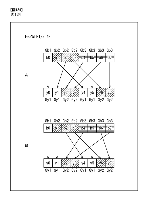
wherein the bit b0 is allocated to the bit yO, the
bit bl to the bit y4, the bit b2 to the bit yl, the bit
b3 to the bit y6, the bit b4 to the bit y2, the bit b5 to
the bit y5, the bit b6 to the bit y3, and the bit b7 to
the bit y7,
wherein a coded rate of the LDPC code having a code
length of 4,320 bits is 1/2,
wherein a parity check matrix of the LDPC code is
configured by arranging elements of l's of an information
matrix that is determined by a parity check matrix
initial value table representing positions of elements of
l's of the information matrix of the parity check matrix
that corresponds to a code length and an information
length according to the coded rate for every 72 columns
in the column direction at a period of 72 columns, and
wherein the parity check matrix initial value table
is formed as follows:
142 150 213 247 507 538 578 828 969 1042 1107 1315
1509 1584 1612 1781 1934 2106 2117
3 17 20 31 97 466 571 580 842 983 1152 1226 1261
1392 1413 1465 1480 2047 2125 49 169 258 548 582 839 873
881 931 995 1145 1209 1639 1654 1776 1826 1865 1906 1956
148 393 396 486 568 806 909 965 1203 1256 1306 1371
1402 1534 1664 1736 1844 1947 2055
16
CA 02809355 2013-02-25
SP311599W000
185 191 263 290 384 769 981 1071 1202 1357 1554
1723 1769 1815 1842 1880 1910 1926 1991
424 444 923 1679
91 436 535 978
362 677 821 1695
1117 1392 1454 2030
35 840 1477 2152
1061 1202 1836 1879
242 286 1140 1538
111 240 481 760
59 1268 1899 2144
737 1299 1395 2072
34 288 810 1903
232 1013 1365 1729
410 783 1066 1187
113 885 1423 1560
760 909 1475 2048
68 254 420 1867
283 325 334 970
168 321 479 554
378 836 1913 1928
101 238 964 1393
304 460 1497 1588
151 192 1075 1614
297 313 677 1303
329 447 1348 1832
582 831 984 1900
[0051]
A data processing device/data processing method
according to a third aspect of the present invention
includes:
17
CA 02809355 2013-02-25
SP311599W000
an interchange means/step that interchanges code
bits of mb bits in accordance with an allocation rule
used for allocating the code bits of an LDPC code to
symbol bits representing a symbol and sets code bits
after interchange as the symbol bits in a case where the
code bits of the LDPC (low density parity check) code
having a code length of N bits are written in a column
direction of a storage means storing the code bits in a
row direction and the column direction, the m bits of the
code bits of the LDPC code read in the row direction are
set as one symbol, a predetermined positive integer is
set as b, the storage means stores the mb bits in the row
direction and stores N/(mb) bits in the column direction,
the code bits of the LDPC code are written in the column
direction of the storage means and then are read in the
row direction, and the code bits of the mb bits read in
the row direction of the storage means form b symbols,
wherein the LDPC code is an LDPC code having a code
length N of 4,320 bits,
wherein the allocation rule is a rule that sets
groups acquired by grouping the code bits of the mb bits
in accordance with an error probability as code bit
groups and groups acquired by grouping the symbol bits of
the mb bits in accordance with an error probability as
symbol bit groups and defines a group set that is a
combination of the code bit group of the code bits and
the symbol bit group of the symbol bits to which the code
bits of the code bit group are allocated and the bit
numbers of the code bits and the symbol bits of each one
of the code bit group and the symbol bit group of the
group set,
18
CA 02809355 2013-02-25
SP311599W000
wherein, in a case where the m bits are four bits,
the integer b is two, and four bits of the code bits are
mapped into one of 16 signal points that are determined
in 16 QAM as one symbol, the code bits of 4 x 2 bits are
grouped into four code bit groups, and the symbol bits of
4 x 2 bits are grouped into two symbol bit groups,
wherein, in the allocation rule, allocation of one
bit of the code bits of the code bit group of which the
error probability is the best to one bit of the symbol
bits of the symbol bit group of which the error
probability is the best, allocation of two bits of the
code bits of the code bit group of which the error
probability is second best to two bits of the symbol bits
of the symbol bit group of which the error probability is
the best, allocation of one bit of the code bits of the
code bit group of which the error probability is second
best to one bit of the symbol bits of the symbol bit
group of which the error probability is second best,
allocation of one bit of the code bits of the code bit
group of which the error probability is third best to one
bit of the symbol bits of the symbol bit group of which
the error probability is the best, and allocation of
three bits of the code bits of the code bit group of
which the error probability is fourth best to three bits
of the symbol bits of the symbol bit group of which the
error probability is second best are defined,
wherein a coded rate of the LDPC code having a code
length of 4,320 bits is 7/12,
wherein a parity check matrix of the LDPC code is
configured by arranging elements of l's of an information
matrix that is determined by a parity check matrix
19
CA 02809355 2013-02-25
SP311599W000
initial value table representing positions of elements of
l's of the information matrix of the parity check matrix
that corresponds to a code length and an information
length according to the coded rate for every 72 columns
in the column direction at a period of 72 columns, and
wherein the parity check matrix initial value table
is formed as follows:
96 246 326 621 668 748 874 965 1022 1108 1117 1142
1300 1469 1481 1627 1702
22 79 122 127 339 359 516 587 1025 1143 1294 1478
1484 1594 1651 1681 1794
80 426 429 506 599 810 892 1016 1117 1246 1277 1281
1316 1384 1713 1729 1753
145 182 305 451 563 570 635 781 827 983 1123
15 1204 1244 1311 1317 1348
11 157 164 292 301 360 636 859 871 895 1138 1164
1206 1268 1454 1613 1783
455 610 1123 1603
631 914 1424 1461
149 507 1275 1468
5 1078 1415 1735
169 772 775 1516
1207 1315 1683 1688
19 1053 1221 1260
933 1095 1597 1628
893 1209 1360 1740
1222 1486 1675 1737
897 1074 1651 1728
115 730 1363 1752
1552 1672 1734 1795
75 1087 1371 1712
20
ak 02809355 2013-02-25
SP311599W000
123 438 839 1074
4 203 1407 1798
441 476 658 1400
380 1341 1741 1774
974 1487 1664 1756
7 273 834 1658
798 1475 1653 1686
12 1237 1539 1709
211 1494 1618 1624
367 1036 1390 1587
18 166 1645 1679
530 1092 1571 1707
588 1593 1689 1707
980 1104 1522 1701
1025 1510 1552 1683
270 340 1326 1770
[0052]
A data processing device/data processing method
according to a fourth aspect of the present invention
includes:
an interchange means/step that interchanges code
bits of mb bits in accordance with an allocation rule
used for allocating the code bits of an LDPC code to
symbol bits representing a symbol and sets code bits
after interchange as the symbol bits in a case where the
code bits of the LDPC (low density parity check) code
having a code length of N bits are written in a column
direction of a storage means storing the code bits in a
row direction and the column direction, the m bits of the
code bits of the LDPC code read in the row direction are
set as one symbol, a predetermined positive integer is
21
CA 02809355 2013-02-25
SP311599W000
set as b, the storage means stores the mb bits in the row
direction and stores N/(mb) bits in the column direction,
the code bits of the LDPC code are written in the column
direction of the storage means and then are read in the
row direction, and the code bits of the mb bits read in
the row direction of the storage means form b symbols,
wherein the LDPC code is an LDPC code having a code
length N of 4,320 bits,
wherein the m bits are four bits, and the integer b
is two,
wherein four bits of the code bits are mapped into
one of 16 signal points that are determined in 16 QAM as
one symbol,
wherein the storage means includes 8 columns
storing 4 x 2 bits in the row direction and stores
4320/(4 x2) bits in the column direction,
wherein, in the interchanging of code bits,
interchanging for allocation according to the allocation
rule is performed with the (#i+1)-th bit from the most
significant bit of the code bits of 4 x 2 bits read in
the row direction of the storage means being bit b#i and
the (#i+1)-th bit from the most significant bit of the
symbol bits of 4 x 2 bits of two consecutive symbols
being bit y4i,
wherein the bit b0 is allocated to the bit yO, the
bit bl to the bit y4, the bit b2 to the bit y5, the bit
b3 to the bit y2, the bit b4 to the bit yl, the bit b5 to
the bit y6, the bit b6 to the bit y3, and the bit b7 to
the bit y7,
wherein a coded rate of the LDPC code having a code
length of 4,320 bits is 7/12,
22
CA 02809355 2013-02-25
SP311599W000
wherein a parity check matrix of the LDPC code is
configured by arranging elements of l's of an information
matrix that is determined by a parity check matrix
initial value table representing positions of elements of
l's of the information matrix of the parity check matrix
that corresponds to a code length and an information
length according to the coded rate for every 72 columns
in the column direction at a period of 72 columns, and
wherein the parity check matrix initial value table
is formed as follows:
96 246 326 621 668 748 874 965 1022 1108 1117 1142
1300 1469 1481 1627 1702
22 79 122 127 339 359 516 587 1025 1143 1294 1478
1484 1594 1651 1681 1794
80 426 429 506 599 810 892 1016 1117 1246 1277 1281
1316 1384 1713 1729 1753
15 145 182 305 451 563 570 635 781 827 983 1123
1204 1244 1311 1317 1348
11 157 164 292 301 360 636 859 871 895 1138 1164
1206 1268 1454 1613 1783
455 610 1123 1603
631 914 1424 1461
149 507 1275 1468
5 1078 1415 1735
169 772 775 1516
1207 1315 1683 1688
19 1053 1221 1260
933 1095 1597 1628
893 1209 1360 1740
1222 1486 1675 1737
897 1074 1651 1728
23
CA 02809355 2013-02-25
SP311599W000
115 730 1363 1752
1552 1672 1734 1795
75 1087 1371 1712
123 438 839 1074
4 203 1407 1798
441 476 658 1400
380 1341 1741 1774
974 1487 1664 1756
7 273 834 1658
798 1475 1653 1686
12 1237 1539 1709
211 1494 1618 1624
367 1036 1390 1587
18 166 1645 1679
530 1092 1571 1707
588 1593 1689 1707
980 1104 1522 1701
1025 1510 1552 1683
270 340 1326 1770
[0053]
A data processing device/data processing method
according to a fifth aspect of the present invention
includes:
an interchange means/step that interchanges code
bits of mb bits in accordance with an allocation rule
used for allocating the code bits of an LDPC code to
symbol bits representing a symbol and sets code bits
after interchange as the symbol bits in a case where the
code bits of the LDPC (low density parity check) code
having a code length of N bits are written in a column
direction of a storage means storing the code bits in a
24
CA 02809355 2013-02-25
SP311599W000
row direction and the column direction, the m bits of the
code bits of the LDPC code read in the row direction are
set as one symbol, a predetermined positive integer is
set as b, the storage means stores the mb bits in the row
direction and stores N/(mb) bits in the column direction,
the code bits of the LDPC code are written in the column
direction of the storage means and then are read in the
row direction, and the code bits of the mb bits read in
the row direction of the storage means form b symbols,
wherein the LDPC code is an LDPC code having a code
length N of 4,320 bits,
wherein the allocation rule is a rule that sets
groups acquired by grouping the code bits of the mb bits
in accordance with an error probability as code bit
groups and groups acquired by grouping the symbol bits of
the mb bits in accordance with an error probability as
symbol bit groups and defines a group set that is a
combination of the code bit group of the code bits and
the symbol bit group of the symbol bits to which the code
bits of the code bit group are allocated and the bit
numbers of the code bits and the symbol bits of each one
of the code bit group and the symbol bit group of the
group set,
wherein, in a case where the m bits are four bits,
the integer b is two, and four bits of the code bits are
mapped into one of 16 signal points that are determined
in 16 QAM as one symbol, the code bits of 4 x 2 bits are
grouped into four code bit groups, and the symbol bits of
4 x 2 bits are grouped into two symbol bit groups,
wherein, in the allocation rule, allocation of one
bit of the code bits of the code bit group of which the
CA 02809355 2013-02-25
SP311599W000
error probability is the best to one bit of the symbol
bits of the symbol bit group of which the error
probability is the best, allocation of three bits of the
code bits of the code bit group of which the error
probability is second best to three bits of the symbol
bits of the symbol bit group of which the error
probability is the best, allocation of one bit of the
code bits of the code bit group of which the error
probability is second best to one bit of the symbol bits
of the symbol bit group of which the error probability is
second best, allocation of one bit of the code bits of
the code bit group of which the error probability is
third best to one bit of the symbol bits of the symbol
bit group of which the error probability is second best,
and allocation of two bits of the code bits of the code
bit group of which the error probability is fourth best
to two bits of the symbol bits of the symbol bit group of
which the error probability is second best are defined,
wherein a coded rate of the LDPC code having a code
length of 4,320 bits is 2/3,
wherein a parity check matrix of the LDPC code is
configured by arranging elements of of an information
matrix that is determined by a parity check matrix
initial value table representing positions of elements of
l's of the information matrix of the parity check matrix
that corresponds to a code length and an information
length according to the coded rate for every 72 columns
in the column direction at a period of 72 columns, and
wherein the parity check matrix initial value table
is formed as follows:
56 291 315 374 378 665 682 713 740 884 923 927 1193
26
CA 02809355 2013-02-25
SP311599W000
1203 1293 1372 1419 1428
1 17 113 402 406 504 559 597 686 697 817 878 983
1007 1034 1142 1231 1431
2 205 350 428 538 605 866 973 1008 1182 1252 1303
1319 1337 1346 1387 1417 1422
50 158 244 424 455 597 830 889 900 945 978 1040
1052 1059 1101 1150 1254 1382 41 53 269 316 449 604 704
752 937 952 1021 1031 1044 1068 1104 1265 1327 1348 601
911 1020-1260
151 674 732 1240
1099 1250 1348 1366
1115 1124 1394 1414
66 250 875 1040
525 603 916 1402
529 561 913 1089
1110 1243 1280 1372
137 656 1316 1369
5 458 1043 1381
1122 1171 1187 1335
18 130 312 1209
534 705 1294
272 727 955 1192
925 1287 1385 1437
11 446 1281 1408
25 614 716 787 1340
615 1147 1411 1416
284 865 1151 1414
202 689 1088 1144
459 633 838 941
30 46 301 1229 1367
476 1031 1120 1418
27
CA 02809355 2013-02-25
SP311599W000
138 336 560 1419
168 357 536 938
1001 1052 1162 1414
349 1039 1353 1426
146 203 530 549
510 545 979 1108
479 1069 1106 1244
743 1019 1275 1348
427 721 1023 1435
73 842 1296 1435
323 1106 1140 1428
1074 1235 1353 1391
[0054]
A data processing device/data processing method
according to a sixth aspect of the present invention
includes:
an interchange means/step that interchanges code
bits of mb bits in accordance with an allocation rule
used for allocating the code bits of an LDPC code to
symbol bits representing a symbol and sets code bits
after interchange as the symbol bits in a case where the
code bits of the LDPC (low density parity check) code
having a code length of N bits are written in a column
direction of a storage means storing the code bits in a
row direction and the column direction, the m bits of the
code bits of the LDPC code read in the row direction are
set as one symbol, a predetermined positive integer is
set as b, the storage means stores the mb bits in the row
direction and stores N/(mb) bits in the column direction,
the code bits of the LDPC code are written in the column
direction of the storage means and then are read in the
28
CA 02809355 2013-02-25
SP311599W000
row direction, and the code bits of the mb bits read in
the row direction of the storage means form b symbols,
wherein the LDPC code is an LDPC code having a code
length N of 4,320 bits,
wherein the m bits are four bits, and the integer b
is two,
wherein four bits of the code bits are mapped into
one of 16 signal points that are determined in 16 QAM as
one symbol,
wherein the storage means includes 8 columns
storing 4 x 2 bits in the row direction and stores
4320/(4 x2) bits in the column direction,
wherein, in the interchanging of code bits,
interchanging for allocation according to the allocation
rule is performed with the (#i+1)-th bit from the most
significant bit of the code bits of 4 x 2 bits read in
the row direction of the storage means being bit b#i and
the (#i+1)-th bit from the most significant bit of the
symbol bits of 4 x 2 bits of two consecutive symbols
being bit y#i,
wherein the bit b0 is allocated to the bit yO, the
bit bl to the bit y4, the bit b2 to the bit y5, the bit
b3 to the bit y2, the bit b4 to the bit yl, the bit b5 to
the bit y6, the bit b6 to the bit y3, and the bit b7 to
the bit y7,
wherein a coded rate of the LDPC code having a code
length of 4,320 bits is 2/3,
wherein a parity check matrix of the LDPC code is
configured by arranging elements of l's of an information
matrix that is determined by a parity check matrix
initial value table representing positions of elements of
29
CA 02809355 2013-02-25
SP311599W000
l's of the information matrix of the parity check matrix
that corresponds to a code length and an information
length according to the coded rate for every 72 columns
in the column direction at a period of 72 columns, and
wherein the parity check matrix initial value table
is formed as follows:
56 291 315 374 378 665 682 713 740 884 923 927 1193
1203 1293 1372 1419 1428
1 17 113 402 406 504 559 597 686 697 817 878 983
1007 1034 1142 1231 1431
2 205 350 428 538 605 866 973 1008 1182 1252 1303
1319 1337 1346 1387 1417 1422
50 158 244 424 455 597 830 889 900 945 978 1040
1052 1059 1101 1150 1254 1382 41 53 269 316 449 604 704
752 937 952 1021 1031 1044 1068 1104 1265 1327 1348 601
= 911 1020 1260
151 674 732 1240
1099 1250 1348 1366
1115 1124 1394 1414
66 250 875 1040
525 603 916 1402
529 561 913 1089
1110 1243 1280 1372
137 656 1316 1369
5 458 1043 1381
1122 1171 1187 1335
18 130 312 1209
534 705 1294
272 727 955 1192
30 925 1287 1385 1437
11 446 1281 1408
30
CA 02809355 2013-02-25
SP311599W000
614 716 787 1340
615 1147 1411 1416
284 865 1151 1414
202 689 1088 1144
459 633 838 941
46 301 1229 1367
476 1031 1120 1418
138 336 560 1419
168 357 536 938
1001 1052 1162 1414
349 1039 1353 1426
146 203 530 549
510 545 979 1108
479 1069 1106 1244
743 1019 1275 1348
427 721 1023 1435
73 842 1296 1435
323 1106 1140 1428
1074 1235 1353 1391
[0055]
A data processing device/data processing method
.according to a seventh aspect of the present invention
includes:
an interchange means/step that interchanges code
bits of mb bits in accordance with an allocation rule
used for allocating the code bits of an LDPC code to
symbol bits representing a symbol and sets code bits
after interchange as the symbol bits in a case where the
code bits of the LDPC (low density parity check) code
having a code length of N bits are written in a column
direction of a storage means storing the code bits in a
31
CA 02809355 2013-02-25
SP311599W000
row direction and the column direction, the m bits of the
code bits of the LDPC code read in the row direction are
set as one symbol, a predetermined positive integer is
set as b, the storage means stores the rob bits in the row
direction and stores N/(mb) bits in the column direction,
the code bits of the LDPC code are written in the column
direction of the storage means and then are read in the
row direction, and the code bits of the mb bits read in
the row direction of the storage means form b symbols,
wherein the LDPC code is an LDPC code having a code
length N of 4,320 bits,
wherein the allocation rule is a rule that sets
groups acquired by grouping the code bits of the rob bits
in accordance with an error probability as code bit
groups and groups acquired by grouping the symbol bits of
the rob bits in accordance with an error probability as
symbol bit groups and defines a group set that is a
combination of the code bit group of the code bits and
the symbol bit group of the symbol bits to which the code
bits of the code bit group are allocated and the bit
numbers of the code bits and the symbol bits of each one
of the code bit group and the symbol bit group of the
group set,
wherein, in a case where the m bits are four bits,
the integer b is two, and four bits of the code bits are
mapped into one of 16 signal points that are determined
in 16 QAM as one symbol, the code bits of 4 x 2 bits are
grouped into three code bit groups, and the symbol bits
of 4 x 2 bits are grouped into two symbol bit groups,
wherein, in the allocation rule, allocation of one
bit of the code bits of the code bit group of which the
32
CA 02809355 2013-02-25
SP311599W000
error probability is the best to one bit of the symbol
bits of the symbol bit group of which the error
probability is the best, allocation of three bits of the
code bits of the code bit group of which the error
probability is second best to three bits of the symbol
bits of the symbol bit group of which the error
probability is the best, allocation of two bits of the
code bits of the code bit group of which the error
probability is second best to two bits of the symbol bits
of the symbol bit group of which the error probability is
second best, and allocation of two bits of the code bits
of the code bit group of which the error probability is
third best to two bits of the symbol bits of the symbol
bit group of which the error probability is second best
are defined,
wherein a coded rate of the LDPC code having a code
length of 4,320 bits is 3/4,
wherein a parity check matrix of the LDPC code is
configured by arranging elements of l's of an information
matrix that is determined by a parity check matrix
initial value table representing positions of elements of
l's of the information matrix of the parity check matrix
that corresponds to a code length and an information
length according to the coded rate for every 72 columns
in the column direction at a period of 72 columns, and
wherein the parity check matrix initial value table
is formed as follows:
3 14 207 304 349 414 577 587 748 761 772 855 920
976 1009 1058 1069
4 61 81 86 136 146 257 392 402 594 812 959 972 1037
1055 1064 1076
33
CA 02809355 2013-02-25
SP311599W000
0 68 160 237 437 512 624 629 652 702 818 858 943
998 1035 1044 1064
42 159 215 254 320 373 382 410 492 630 887 889
911 916 975 1069
5 12 32 298 302 318 425 558 621 670 779 964 967 970
975 1054 1067 1072
124 381 715 981
503 610 633 1030
321 874 900 1020
10 509 817 902 978
3 118 688 911
515 644 848 1067
13 75 721 970
9 464 756 1023
26 219 304 672
5 310 410 695
0 7 267 1040
76 822 873 1043
7 129 1010 1065
115 156 714 1003
163 480 505 1079
238 601 743 1046
216 702 738 912
13 20 166 979
11 14 261 1051
186 476 595 843
13 237 451 532
7 11 594 738
10 225 495 851
520 675 1018 1045
9 352 514 543
34
CA 02809355 2013-02-25
SP311599W000
60 917 1071 1074
471 556 673 1062
345 350 1043 1076
539 788 1061
5 704 851 883 1049
211 233 242 1072
9 1047 1057 1076
18 172 473 1042
365 488 921 968
211 216 554 824
1 709 923 1074
576 647 901 963
71 676 1053 1073
265 738 958 969
66 274 774 811
[0056]
A data processing device/data processing method
according to an eighth aspect of the present invention
includes:
an interchange means/step that interchanges code
bits of rob bits in accordance with an allocation rule
used for allocating the code bits of an LDPC code to
symbol bits representing a symbol and sets code bits
after interchange as the symbol bits in a case where the
code bits of the LDPC (low density parity check) code
having a code length of N bits are written in a column
direction of a storage means storing the code bits in a
row direction and the column direction, the m bits of the
code bits of the LDPC code read in the row direction are
set as one symbol, a predetermined positive integer is
set as b, the storage means stores the rob bits in the row
35
CA 02809355 2013-02-25
SP311599W000
direction and stores N/(mb) bits in the column direction,
the code bits of the LDPC code are written in the column
direction of the storage means and then are read in the
row direction, and the code bits of the mb bits read in
the row direction of the storage means form b symbols,
wherein the LDPC code is an LDPC code having a code
length N of 4,320 bits,
wherein the m bits are four bits, and the integer b
is two, -
wherein four bits of the code bits are mapped into
one of 16 signal points that are determined in 16 QAM as
one symbol,
wherein the storage means includes 8 columns
storing 4 x 2 bits in the row direction and stores
4320/(4 x2) bits in the column direction,
wherein, in the interchanging of code bits,
interchanging for allocation according to the allocation
rule is performed with the (#i+1)-th bit from the most
significant bit of the code bits of 4 x 2 bits read in
the row direction of the storage means being bit b#i and
the (#i+1)-th bit from the most significant bit of the
symbol bits of 4 x 2 bits of two consecutive symbols
being bit y#i,
wherein the bit b0 is allocated to the bit yO, the
bit b1 to the bit y4, the bit b2 to the bit y5, the bit
b3 to the bit y2, the bit b4 to the bit yl, the bit b5 to
the bit y6, the bit b6 to the bit y3, and the bit b7 to
the bit y7,
wherein a coded rate of the LDPC code having a code
length of 4,320 bits is 3/4,
wherein a parity check matrix of the LDPC code is
36
CA 02809355 2013-02-25
SP311599W000
configured by arranging elements of l's of an information
matrix that is determined by a parity check matrix
initial value table representing positions of elements of
l's of the information matrix of the parity check matrix
that corresponds to a code length and an information
length according to the coded rate for every 72 columns
in the column direction at a period of 72 columns, and
wherein the parity check matrix initial value table
is formed as follows:
3 14 207 304 349 414 577 587 748 761 772 855 920
976 1009 1058 1069
4 61 81 86 136 146 257 392 402 594 812 959 972 1037
1055 1064 1076
0 68 160 237 437 512 624 629 652 702 818 858 943
998 1035 1044 1064
10 42 159 215 254 320 373 382 410 492 630 887 889
911 916 975 1069
12 32 298 302 318 425 558 621 670 779 964 967 970
975 1054 1067 1072
124 381 715 981
503 610 633 1030
321 874 900 1020
509 817 902 978
3 118 688 911
515 644 848 1067
13 75 721 970
9 464 756 1023
26 219 304 672
5 310 410 695
0 7 267 1040
76 822 873 1043
37
CA 02809355 2013-02-25
SP311599W000
7 129 1010 1065
115 156 714 1003
163 480 505 1079
238 601 743 1046
216 702 738 912
13 20 166 979
11 14 261 1051
186 476 595 843
13-237 451 532
7 11 594 738
10 225 495 851
520 675 1018 1045
9 352 514 543
60 917 1071 1074
471 556 673 1062
345 350 1043 1076
5 539 788 1061
704 851 883 1049
211 233 242 1072
9 1047 1057 1076
18 172 473 1042
365 488 921 968
211 216 554 824
1 709 923 1074
576 647 901 963
71 676 1053 1073
265 738 958 969
66 274 774 811
[0057]
A data processing device according to a ninth
aspect of the present invention includes:
38
CA 02809355 2013-02-25
SP311599W000
an interchange means that interchanges code bits of
mb bits in accordance with an allocation rule used for
allocating the code bits of an LDPC code to symbol bits
representing a symbol and sets code bits after
interchange as the symbol bits in a case where the code
bits of the LDPC (low density parity check) code having a
code length of N bits are written in a column direction
of a storage means storing the code bits in a row
direction and the column direction, the m bits of the
code bits of the LDPC code read in the row direction are
set as one symbol, a predetermined positive integer is
set as b, the storage means stores the mb bits in the row
direction and stores N/(mb) bits in the column direction,
the code bits of the LDPC code are written in the column
direction of the storage means and then are read in the
row direction, and the code bits of the mb bits read in
the row direction of the storage means form b symbols;
and
a reverse interchanging means that performs a
reverse interchanging process in which the positions of
the code bits after interchange, which are acquired from
a transmission device, are returned to the original
positions,
wherein the LDPC code is an LDPC code having a code
length N of 4,320 bits,
wherein the m bits are four bits, and the integer b
is two,
wherein four bits of the code bits are mapped into
one of 16 signal points that are determined in 16 QAM as
one symbol,
wherein the storage means includes 8 columns
39
CA 02809355 2013-02-25
SP311599W000
storing 4 x 2 bits in the row direction and stores
4320/(4 x 2) bits in the column direction,
wherein the interchange means performs
interchanging for allocation according to the allocation
rule with the (#i+1)-th bit from the most significant bit
of the code bits of 4 x 2 bits read in the row direction
of the storage means being bit b#i and the (#i+1)-th bit
from the most significant bit of the symbol bits of 4 x 2
bits of two consecutive symbols being bit y#i,
wherein the bit b0 is allocated to the bit yO, the
bit bl to the bit y4, the bit b2 to the bit yl, the bit
b3 to the bit y6, the bit b4 to the bit y2, the bit b5 to
the bit y5, the bit b6 to the bit y3, and the bit b7 to
the bit y7,
wherein a coded rate of the LDPC code having a code
length of 4,320 bits is 1/2,
wherein a parity check matrix of the LDPC code is
configured by arranging elements of l's of an information
matrix that is determined by a parity check matrix
initial value table representing positions of elements of
l's of the information matrix of the parity check matrix
that corresponds to a code length and an information
length according to the coded rate for every 72 columns
in the column direction at a period of 72 columns, and
wherein the parity check matrix initial value table
is formed as follows:
142 150 213 247 507 538 578 828 969 1042 1107 1315
1509 1584 1612 1781 1934 2106 2117
3 17 20 31 97 466 571 580 842 983 1152 1226 1261
1392 1413 1465 1480 2047 2125 49 169 258 548 582 839 873
881 931 995 1145 1209 1639 1654 1776 1826 1865 1906 1956
40
CA 02809355 2013-02-25
SP311599W000
148 393 396 486 568 806 909 965 1203 1256 1306 1371
1402 1534 1664 1736 1844 1947 2055
185 191 263 290 384 769 981 1071 1202 1357 1554
1723 1769 1815 1842 1880 1910 1926 1991
424 444 923 1679
91 436 535 978
362 677 821 1695
1117 1392 1454 2030
35-840 1477 2152
1061 1202 1836 1879
242 286 1140 1538
111 240 481 760
59 1268 1899 2144
737 1299 1395 2072
34 288 810 1903
232 1013 1365 1729
410 783 1066 1187
113 885 1423 1560
760 909 1475 2048
68 254 420 1867
283 325 334 970
168 321 479 554
378 836 1913 1928
101 238 964 1393
304 460 1497 1588
151 192 1075 1614
297 313 677 1303
329 447 1348 1832
582 831 984 1900
[0058]
A data processing device according to a tenth
41
CA 02809355 2013-02-25
SP311599W000
aspect of the present invention includes:
an interchange means that interchanges code bits of
mb bits in accordance with an allocation rule used for
allocating the code bits of an LDPC code to symbol bits
representing a symbol and sets code bits after
interchange as the symbol bits in a case where the code
bits of the LDPC (low density parity check) code having a
code length of N bits are written in a column direction
of a storage means storing the code bits in a row
direction and the column direction, the m bits of the
code bits of the LDPC code read in the row direction are
set as one symbol, a predetermined positive integer is
set as b, the storage means stores the mb bits in the row
direction and stores N/(mb) bits in the column direction,
the code bits of the LDPC code are written in the column
direction of the storage means and then are read in the
row direction, and the code bits of the mb bits read in
the row direction of the storage means form b symbols;
and
a reverse interchanging means that performs a
reverse interchanging process in which the positions of
the code bits after interchange, which are acquired from
a transmission device, are returned to the original
positions,
wherein the LDPC code is an LDPC code having a code
length N of 4,320 bits,
wherein the m bits are four bits, and the integer b
is two,
wherein four bits of the code bits are mapped into
one of 16 signal points that are determined in 16 QAM as
one symbol,
42
CA 02809355 2013-02-25
SP311599W000
wherein the storage means includes 8 columns
storing 4 x 2 bits in the row direction and stores
4320/(4 x 2) bits in the column direction,
wherein the interchange means performs
interchanging for allocation according to the allocation
rule with the (#i+1)-th bit from the most significant bit
of the code bits of 4 x 2 bits read in the row direction
of the storage means being bit b#i and the (#i+1)-th bit
from the-most significant bit of the symbol bits of 4 x 2
bits of two consecutive symbols being bit y#i,
wherein the bit b0 is allocated to the bit yO, the
bit bl to the bit y4, the bit b2 to the bit y5, the bit
b3 to the bit y2, the bit b4 to the bit yl, the bit b5 to
the bit y6, the bit b6 to the bit y3, and the bit b7 to
the bit y7,
wherein a coded rate of the LDPC code having a code
length of 4,320 bits is 7/12,
wherein a parity check matrix of the LDPC code is
configured by arranging elements of of an information
matrix that is determined by a parity check matrix
initial value table representing positions of elements of
l's of the information matrix of the parity check matrix
that corresponds to a code length and an information
length according to the coded rate for every 72 columns
in the column direction at a period of 72 columns, and
wherein the parity check matrix initial value table
is formed as follows:
96 246 326 621 668 748 874 965 1022 1108 1117 1142
1300 1469 1481 1627 1702
22 79 122 127 339 359 516 587 1025 1143 1294 1478
1484 1594 1651 1681 1794
43
CA 02809355 2013-02-25
SP311599W000
80 426 429 506 599 810 892 1016 1117 1246 1277 1281
1316 1384 1713 1729 1753
15 145 182 305 451 563 570 635 781 827 983 1123
1204 1244 1311 1317 1348
11 157 164 292 301 360 636 859 871 895 1138 1164
1206 1268 1454 1613 1783
455 610 1123 1603
631 914 1424 1461
149 507 1275 1468
5 1078 1415 1735
169 772 775 1516
1207 1315 1683 1688
19 1053 1221 1260
933 1095 1597 1628
893 1209 1360 1740
1222 1486 1675 1737
897 1074 1651 1728
115 730 1363 1752
1552 1672 1734 1795
75 1087 1371 1712
123 438 839 1074
4 203 1407 1798
441 476 658 1400
380 1341 1741 1774
974 1487 1664 1756
7 273 834 1658
798 1475 1653 1686
12 1237 1539 1709
211 1494 1618 1624
367 1036 1390 1587
18 166 1645 1679
44
CA 02809355 2013-02-25
SP311599W000
530 1092 1571 1707
588 1593 1689 1707
980 1104 1522 1701
1025 1510 1552 1683
270 340 1326 1770
[0059]
A data processing device according to an eleventh
aspect of the present invention includes:
an-interchange means that interchanges code bits of
mb bits in accordance with an allocation rule used for
allocating the code bits of an LDPC code to symbol bits
representing a symbol and sets code bits after
interchange as the symbol bits in a case where the code
bits of the LDPC (low density parity check) code having a
code length of N bits are written in a column direction
of a storage means storing the code bits in a row
direction and the column direction, the m bits of the
code bits of the LDPC code read in the row direction are
set as one symbol, a predetermined positive integer is
set as b, the storage means stores the mb bits in the row
direction and stores N/(mb) bits in the column direction,
the code bits of the LDPC code are written in the column
direction of the storage means and then are read in the
row direction, and the code bits of the mb bits read in
the row direction of the storage means form b symbols;
and
a reverse interchanging means that performs a
reverse interchanging process in which the positions of
the code bits after interchange, which are acquired from
a transmission device, are returned to the original
positions,
45
CA 02809355 2013-02-25
SP311599W000
wherein the LDPC code is an LDPC code having a code
length N of 4,,320 bits,
wherein the m bits are four bits, and the integer b
is two,
wherein four bits of the code bits are mapped into
one of 16 signal points that are determined in 16 QAM as
one symbol,
wherein the storage means includes 8 columns
storing 4 x 2 bits in the row direction and stores
4320/(4 x 2) bits in the column direction,
wherein the interchange means performs
interchanging for allocation according to the allocation
rule with the (#i+1)-th bit from the most significant bit
of the code bits of 4 x 2 bits read in the row direction
of the storage means being bit b#i and the (#i+1)-th bit
from the most significant bit of the symbol bits of 4 x 2
bits of two consecutive symbols being bit y#i,
wherein the bit b0 is allocated to the bit yO, the
bit bl to the bit y4, the bit b2 to the bit y5, the bit
b3 to the bit y2, the bit b4 to the bit yl, the bit b5 to
the bit y6, the bit b6 to the bit y3, and the bit b7 to
the bit y7,
wherein a coded rate of the LDPC code having a code
length of 4,320 bits is 2/3,
wherein a parity check matrix of the LDPC code is
configured by arranging elements of l's of an information
matrix that is determined by a parity check matrix
initial value table representing positions of elements of
l's of the information matrix of the parity check matrix
that corresponds to a code length and an information
length according to the coded rate for every 72 columns
46
CA 02809355 2013-02-25
SP311599W000
in the column direction at a period of 72 columns, and
wherein the parity check matrix initial value table
is formed as follows:
56 291 315 374 378 665 682 713 740 884 923 927 1193
1203 1293 1372 1419 1428
1 17 113 402 406 504 559 597 686 697 817 878 983
1007 1034 1142 1231 1431
2 205 350 428 538 605 866 973 1008 1182 1252 1303
1319 1337 1346 1387 1417 1422
50 158 244 424 455 597 830 889 900 945 978 1040
1052 1059 1101 1150 1254 1382 41 53 269 316 449 604 704
752 937 952 1021 1031 1044 1068 1104 1265 1327 1348 601
911 1020 1260
151 674 732 1240
1099 1250 1348 1366
1115 1124 1394 1414
66 250 875 1040
525 603 916 1402
529 561 913 1089
1110 1243 1280 1372
137 656 1316 1369
5 458 1043 1381
1122 1171 1187 1335
18 130 312 1209
30 534 705 1294
272 727 955 1192
925 1287 1385 1437
11 446 1281 1408
614 716 787 1340
615 1147 1411 1416
284 865 1151 1414
47
CA 02809355 2013-02-25
SP311599W000
202 689 1088 1144
459 633 838 941
46 301 1229 1367
476 1031 1120 1418
138 336 560 1419
168 357 536 938
1001 1052 1162 1414
349 1039 1353 1426
146 203 530 549
510 545 979 1108
479 1069 1106 1244
743 1019 1275 1348
427 721 1023 1435
73 842 1296 1435
323 1106 1140 1428
1074 1235 1353 1391
[0060]
A data processing device according to a twelfth
aspect of the present invention includes:
an interchange means that interchanges code bits of
mb bits in accordance with an allocation rule used for
allocating the code bits of an LDPC code to symbol bits
representing a symbol and sets code bits after
interchange as the symbol bits in a case where the code
bits of the LDPC (low density parity check) code having a
code length of N bits are written in a column direction
of a storage means storing the code bits in a row
direction and the column direction, the m bits of the
code bits of the LDPC code read in the row direction are
set as one symbol, a predetermined positive integer is
set as b, the storage means stores the mb bits in the row
48
CA 02809355 2013-02-25
SP311599W000
direction and stores N/(mb) bits in the column direction,
the code bits of the LDPC code are written in the column
direction of the storage means and then are read in the
row direction, and the code bits of the mb bits read in
the row direction of the storage means form b symbols;
and
a reverse interchanging means that performs a
reverse interchanging process in which the positions of
the code bits after interchange, which are acquired from
a transmission device, are returned to the original
positions,
wherein the LDPC code is an LDPC code having a code
length N of 4,320 bits,
wherein the m bits are four bits, and the integer b
is two,
wherein four bits of the code bits are mapped into
one of 16 signal points that are determined in 16 QAM as
one symbol,
wherein the storage means includes 8 columns
storing 4 x 2 bits in the row direction and stores
4320/(4 x 2) bits in the column direction,
wherein the interchange means performs
interchanging for allocation according to the allocation
rule with the (#i+1)-th bit from the most significant bit
of the code bits of 4 x 2 bits read in the row direction
of the storage means being bit b#i and the (#i+1)-th bit
from the most significant bit of the symbol bits of 4 x 2
bits of two consecutive symbols being bit y#i,
wherein the bit b0 is allocated to the bit yO, the
bit bl to the bit y4, the bit b2 to the bit y5, the bit
b3 to the bit y2, the bit b4 to the bit yl, the bit b5 to
49
CA 02809355 2013-02-25
SP311599W000
the bit y6, the bit b6 to the bit y3, and the bit b7 to
the bit y7,
wherein a coded rate of the LDPC code having a code
length of 4,320 bits is 3/4,
wherein a parity check matrix of the LDPC code is
configured by arranging elements of l's of an information
matrix that is determined by a parity check matrix
initial value table representing positions of elements of
l's of the information matrix of the parity check matrix
that corresponds to a code length and an information
length according to the coded rate for every 72 columns
in the column direction at a period of 72 columns, and
wherein the parity check matrix initial value table
is formed as follows:
3 14 207 304 349 414 577 587 748 761 772 855 920
976 1009 1058 1069
4 61 81 86 136 146 257 392 402 594 812 959 972 1037
1055 1064 1076
998 1035 1044 10640 68 160 237 437 512 624 629 652 702 818 858 943
10 42 159 215 254 320 373 382 410 492 630 887 889
911 916 975 1069
12 32 298 302 318 425 558 621 670 779 964 967 970
975 1054 1067 1072
124 381 715 981
503 610 633 1030
321 874 900 1020
509 817 902 978
3 118 688 911
515 644 848 1067
13 75 721 970
50
CA 02809355 2013-02-25
SP311599W000
9 464 756 1023
26 219 304 672
310 410 695
0 7 267 1040
5 76 822 873 1043
7 129 1010 1065
115 156 714 1003
163 480 505 1079
238 601 743 1046
216 702 738 912
13 20 166 979
11 14 261 1051
186 476 595 843
13 237 451 532
7 11 594 738
10 225 495 851
520 675 1018 1045
9 352 514 543
60 917 1071 1074
471 556 673 1062
345 350 1043 1076
5 539 788 1061
704 851 883 1049
211 233 242 1072
9 1047 1057 1076
18 172 473 1042
365 488 921 968
211 216 554 824
1 709 923 1074
576 647 901 963
71 676 1053 1073
51
CA 02809355 2013-02-25
SP311599W000
265 738 958 969
66 274 774 811
[0061]
According to the first to eighth aspects of the
invention, code bits of mb bits are interchanged in
accordance with an allocation rule used for allocating
the code bits of an LDPC code to symbol bits representing
a symbol and code bits after interchange are set as the
symbol bits in a case where the code bits of the LDPC
(low density parity check) code having a code length of N
bits are written in a column direction of a storage means
storing the code bits in a row direction and the column
direction, the m bits of the code bits of the LDPC code
read in the row direction are set as one symbol, a
predetermined positive integer is set as b, the storage
means stores the mb bits in the row direction and stores
N/(mb) bits in the column direction, the code bits of the
LDPC code are written in the column direction of the
storage means and then are read in the row direction, and
the code bits of the mb bits read in the row direction of
the storage means form b symbols.
[0062]
The LDPC code is an LDPC code having a code length
N of 4,320 bits, and the allocation rule is a rule that
sets groups acquired by grouping the code bits of the mb
bits in accordance with an error probability as code bit
groups and groups acquired by grouping the symbol bits of
the mb bits in accordance with an error probability as
symbol bit groups and defines a group set that is a
combination of the code bit group of the code bits and
the symbol bit group of the symbol bits to which the code
52
CA 02809355 2013-02-25
SP311599W000
bits of the code bit group are allocated and the bit
numbers of the code bits and the symbol bits of each one
of the code bit group and the symbol bit group of the
group set.
[0063]
In addition, the m bits are four bits, the integer
b is two, and four bits of the code bits are mapped into
one of 16 signal points determined in 16 QAM as the one
symbol. -
[0064]
According to the first aspect, the code bits of 4 x
2 bits are grouped into three code bit groups, and the
symbol bits of 4 x 2 bits are grouped into two symbol bit
groups, and the code bits are interchanged in accordance
with the allocation rule in which allocation of one bit
of the code bits of the code bit group of which the error
probability is the best to one bit of the symbol bits of
the symbol bit group of which the error probability is
the best, allocation of two bits of the code bits of the
code bit group of which the error probability is second
best to two bits of the symbol bits of the symbol bit
group of which the error probability is the best,
allocation of one bit of the code bits of the code bit
group of which the error probability is second best to
one bit of the symbol bits of the symbol bit group of
which the error probability is second best, allocation of
one bit of the code bits of the code bit group of which
the error probability is third best to one bit of the
symbol bits of the symbol bit group of which the error
probability is the best, and allocation of three bits of
the code bits of the code bit group of which the error
53
CA 02809355 2013-02-25
SP311599W000
probability is third best to three bits of the symbol
bits of the symbol bit group of which the error
probability is second best are defined.
[0065]
According to the second aspect, 8 columns storing 4
x 2 bits in the row direction are included, the (#i+1)-th
bit from the most significant bit of the code bits of 4 x
2 bits read in the row direction of the storage means,
which stOres 4,320/(4 x 2) bits in the column direction,
is set as bit b#i, the (#i+1)-th bit from the most
significant bit of the symbol bits of 4 x 2 bits of two
consecutive symbols is set as bit y#i, and interchange is
performed in accordance with the allocation rule in which
bit b0 is allocated to bit yO, bit b1 is allocated to bit
y4, bit b2 is allocated to bit yl, bit b3 is allocated to
bit y6, bit b4 is allocated to bit y2, bit b5 is
allocated to bit y5, bit b6 is allocated to bit y3, and
bit b7 is allocated to bit y7.
[0066]
Here, according to the first and second aspects, a
coded rate of the LDPC code having a code length of 4,320
bits is 1/2, a parity check matrix of the LDPC code is
configured by arranging elements of l's of an information
matrix that is determined by a parity check matrix
initial value table representing positions of elements of
l's of the information matrix of the parity check matrix
that corresponds to a code length and an information
length according to the coded rate for every 72 columns
in the column direction at a period of 72 columns, and
the parity check matrix initial value table is formed as
follows.
54
CA 02809355 2013-02-25
SP311599W000
142 150 213 247 507 538 578 828 969 1042 1107 1315
1509 1584 1612 1781 1934 2106 2117
3 17 20 31 97 466 571 580 842 983 1152 1226 1261
1392 1413 1465 1480 2047 2125 49 169 258 548 582 839 873
881 931 995 1145 1209 1639 1654 1776 1826 1865 1906 1956
148 393 396 486 568 806 909 965 1203 1256 1306 1371
1402 1534 1664 1736 1844 1947 2055
185 191 263 290 384 769 981 1071 1202 1357 1554
1723 1769 1815 1842 1880 1910 1926 1991
424 444 923 1679
91 436 535 978
362 677 821 1695
1117 1392 1454 2030
35 840 1477 2152
1061 1202 1836 1879
242 286 1140 1538
111 240 481 760
59 1268 1899 2144
737 1299 1395 2072
34 288 810 1903
232 1013 1365 1729
410 783 1066 1187
113 885 1423 1560
760 909 1475 2048
68 254 420 1867
283 325 334 970
168 321 479 554
378 836 1913 1928
101 238 964 1393
304 460 1497 1588
151 192 1075 1614
CA 02809355 2013-02-25
SP311599W000
297 313 677 1303
329 447 1348 1832
582 831 984 1900
[0067]
According to the third aspect, the code bits of 4 x
2 bits are grouped into four code bit groups, the symbol
bits of 4 x2 bits are grouped into two symbol bit groups,
and the code bits are interchanged in accordance with the
allocation rule in which allocation of one bit of the
code bits of the code bit group of which the error
probability is the best to one bit of the symbol bits of
the symbol bit group of which the error probability is
the best, allocation of two bits of the code bits of the
code bit group of which the error probability is second
best to two bits of the symbol bits of the symbol bit
group of which the error probability is the best,
allocation of one bit of the code bits of the code bit
group of which the error probability is second best to
one bit of the symbol bits of the symbol bit group of
which the error probability is second best, allocation of
one bit of the code bits of the code bit group of which
the error probability is third best to one bit of the
symbol bits of the symbol bit group of which the error
probability is the best, and allocation of three bits of
the code bits of the code bit group of which the error
probability is fourth best to three bits of the symbol
bits of the symbol bit group of which the error
probability is second best are defined.
[0068]
According to the fourth aspect, 8 columns storing 4
x 2 bits in the row direction are included, the (#i+1)-th
56
CA 02809355 2013-02-25
SP311599W000
bit from the most significant bit of the code bits of 4 x
2 bits read in the row direction of the storage means,
which stores 4,320/(4 x 2) bits in the column direction,
is set as bit b#i, the (#i+1)-th bit from the most
significant bit of the symbol bits of 4 x 2 bits of two
consecutive symbols is set as bit y#i, and interchange is
performed in accordance with the allocation rule in which
bit b0 is allocated to bit yO, bit bl is allocated to bit
y4, bit b2 is allocated to bit y5, bit b3 is allocated to
bit y2, bit b4 is allocated to bit yl, bit b5 is
allocated to bit y6, bit b6 is allocated to bit y3, and
bit b7 is allocated to bit y7.
[0069]
Here, according to the third and fourth aspects, a
coded rate of the LDPC code having a code length of 4,320
bits is 7/12, a parity check matrix of the LDPC code is
configured by arranging elements of l's of an information
matrix that is determined by a parity check matrix
initial value table representing positions of elements of
l's of the information matrix of the parity check matrix
that corresponds to a code length and an information
length according to the coded rate for every 72 columns
in the column direction at a period of 72 columns, and
the parity check matrix initial value table is formed as
follows.
96 246 326 621 668 748 874 965 1022 1108 1117 1142
1300 1469 1481 1627 1702
22 79 122 127 339 359 516 587 1025 1143 1294 1478
1484 1594 1651 1681 1794
80 426 429 506 599 810 892 1016 1117 1246 1277 1281
1316 1384 1713 1729 1753
57
CA 02809355 2013-02-25
SP311599W000
15 145 182 305 451 563 570 635 781 827 983 1123
1204 1244 1311 1317 1348
11 157 164 292 301 360 636 859 871 895 1138 1164
1206 1268 1454 1613 1783
455 610 1123 1603
631 914 1424 1461
149 507 1275 1468
5 1078 1415 1735
169 772 775 1516
1207 1315 1683 1688
19 1053 1221 1260
933 1095 1597 1628
893 1209 1360 1740
1222 1486 1675 1737
897 1074 1651 1728
115 730 1363 1752
1552 1672 1734 1795
75 1087 1371 1712
123 438 839 1074
4 203 1407 1798
441 476 658 1400
380 1341 1741 1774
974 1487 1664 1756
7 273 834 1658
798 1475 1653 1686
12 1237 1539 1709
211 1494 1618 1624
367 1036 1390 1587
18 166 1645 1679
530 1092 1571 1707
588 1593 1689 1707
58
CA 02809355 2013-02-25
SP311599W000
980 1104 1522 1701
1025 1510 1552 1683
270 340 1326 1770
[0070]
According to the fifth aspect, the code bits of 4 x
2 bits are grouped into four code bit groups, the symbol
bits of 4 x 2 bits are grouped into two symbol bit groups,
and the code bits are interchanged in accordance with the
allocation rule in which allocation of one bit of the
code bits of the code bit group of which the error
probability is the best to one bit of the symbol bits of
the symbol bit group of which the error probability is
the best, allocation of three bits of the code bits of
the code bit group of which the error probability is
second best to three bits of the symbol bits of the
symbol bit group of which the error probability is the
best, allocation of one bit of the code bits of the code
bit group of which the error probability is second best
to one bit of the symbol bits of the symbol bit group of
which the error probability is second best, allocation of
one bit of the code bits of the code bit group of which
the error probability is third best to one bit of the
symbol bits of the symbol bit group of which the error
probability is second best, and allocation of two bits of
the code bits of the code bit group of which the error
probability is fourth best to two bits of the symbol bits
of the symbol bit group of which the error probability is
second best are defined.
[0071]According to the sixth aspect, 8 columns storing 4
x 2 bits in the row direction are included, the (#i+1)-th
59
CA 02809355 2013-02-25
SP311599W000
bit from the most significant bit of the code bits of 4 x
2 bits read in the row direction of the storage means,
which stores 4,320/(4 x 2) bits in the column direction,
is set as bit b#i, the (#i+1)-th bit from the most
significant bit of the symbol bits of 4 x 2 bits of two
consecutive symbols is set as bit y#i, and interchange is
performed in accordance with the allocation rule in which
bit b0 is allocated to bit yO, bit bl is allocated to bit
y4, bit b2 is allocated to bit y5, bit b3 is allocated to
bit y2, bit b4 is allocated to bit yl, bit b5 is
allocated to bit y6, bit b6 is allocated to bit y3, and
bit b7 is allocated to bit y7.
[0072]
Here, according to the fifth and sixth aspects, a
coded rate of the LDPC code having a code length of 4,320
bits is 2/3, a parity check matrix of the LDPC code is
configured by arranging elements of l's of an information
matrix that is determined by a parity check matrix
initial value table representing positions of elements of
l's of the information matrix of the parity check matrix
that corresponds to a code length and an information
length according to the coded rate for every 72 columns
in the column direction at a period of 72 columns, and
the parity check matrix initial value table is formed as
follows.
56 291 315 374 378 665 682 713 740 884 923 927 1193
1203 1293 1372 1419 1428
1 17 113 402 406 504 559 597 686 697 817 878 983
1007 1034 1142 1231 1431
2 205 350 428 538 605 866 973 1008 1182 1252 1303
1319 1337 1346 1387 1417 1422
CA 02809355 2013-02-25
SP311599W000
50 158 244 424 455 597 830 889 900 945 978 1040
1052 1059 1101 1150 1254 1382 41 53 269 316 449 604 704
752 937 952 1021 1031 1044 1068 1104 1265 1327 1348 601
911 1020 1260
151 674 732 1240
1099 1250 1348 1366
1115 1124 1394 1414
66 250 875 1040
525 603 916 1402
529 561 913 1089
1110 1243 1280 1372
137 656 1316 1369
5 458 1043 1381
1122 1171 1187 1335
18 130 312 1209
30 534 705 1294
272 727 955 1192
925 1287 1385 1437
11 446 1281 1408
614 716 787 1340
615 1147 1411 1416
284 865 1151 1414
202 689 1088 1144
459 633 838 941
46 301 1229 1367
476 1031 1120 1418
138 336 560 1419
168 357 536 938
1001 1052 1162 1414
349 1039 1353 1426
146 203 530 549
61
CA 02809355 2013-02-25
SP311599W000
510 545 979 1108
479 1069 1106 1244
743 1019 1275 1348
427 721 1023 1435
73 842 1296 1435
323 1106 1140 1428
1074 1235 1353 1391
[0073]
According to the seventh aspect, the code bits of 4
x 2 bits are grouped into three code bit groups, the
symbol bits of 4 x 2 bits are grouped into two symbol bit
groups, and the code bits are interchanged in accordance
with the allocation rule in which allocation of one bit
of the code bits of the code bit group of which the error
probability is the best to one bit of the symbol bits of
the symbol bit group of which the error probability is
the best, allocation of three bits of the code bits of
the code bit group of which the error probability is
second best to three bits of the symbol bits of the
symbol bit group of which the error probability is the
best, allocation of two bits of the code bits of the code
bit group of which the error probability is second best
to two bits of the symbol bits of the symbol bit group of
which the error probability is second best, and
allocation of two bits of the code bits of the code bit
group of which the error probability is third best to two
bits of the symbol bits of the symbol bit group of which
the error probability is second best are defined.
[0074]
According to the eighth aspect, 8 columns storing 4
x 2 bits in the row direction are included, the (#i+1)-th
62
CA 02809355 2013-02-25
SP311599W000
bit from the most significant bit of the code bits of 4 x
2 bits read in the row direction of the storage means,
which stores 4,320/(4 x 2) bits in the column direction,
is set as bit b#i, the (#i+1)-th bit from the most
significant bit of the symbol bits of 4 x 2 bits of two
consecutive symbols is set as bit y#i, and interchange is
performed in accordance with the allocation rule in which
bit b0 is allocated to bit yO, bit bl is allocated to bit
y4, bit b2 is allocated to bit y5, bit b3 is allocated to
bit y2, bit b4 is allocated to bit yl, bit b5 is
allocated to bit y6, bit b6 is allocated to bit y3, and
bit b7 is allocated to bit y7.
[0075]
Here, according to the seventh and eighth aspects,
a coded rate of the LDPC code having a code length of
4,320 bits is 3/4, a parity check matrix of the LDPC code
is configured by arranging elements of of an
information matrix that is determined by a parity check
matrix initial value table representing positions of
elements of l's of the information matrix of the parity
check matrix that corresponds to a code length and an
information length according to the coded rate for every
72 columns in the column direction at a period of 72
columns, and the parity check matrix initial value table
is formed as follows.
3 14 207 304 349 414 577 587 748 761 772 855 920
976 1009 1058 1069
4 61 81 86 136 146 257 392 402 594 812 959 972 1037
1055 1064 1076
0 68 160 237 437 512 624 629 652 702 818 858 943
998 1035 1044 1064
63
CA 02809355 2013-02-25
SP311599W000
42 159 215 254 320 373 382 410 492 630 887 889
911 916 975 1069
12 32 298 302 318 425 558 621 670 779 964 967 970
975 1054 1067 1072
5 124 381 715 981
503 610 633 1030
321 874 900 1020
509 817 902 978
3 118 688 911
10 515 644 848 1067
13 75 721 970
9 464 756 1023
26 219 304 672
5 310 410 695
0 7 267 1040
76 822 873 1043
7 129 1010 1065
115 156 714 1003
163 480 505 1079
238 601 743 1046
216 702 738 912
13 20 166 979
11 14 261 1051
186 476 595 843
13 237 451 532
7 11 594 738
10 225 495 851
520 675 1018 1045
9 352 514 543
60 917 1071 1074
471 556 673 1062
64
CA 02809355 2013-02-25
SP311599W000
345 350 1043 1076
539 788 1061
704 851 883 1049
211 233 242 1072
5 9 1047 1057 1076
18 172 473 1042
365 488 921 968
211 216 554 824
1 709 923 1074
576 647 901 963
71 676 1053 1073
265 738 958 969
66 274 774 811
[0076]
According to the ninth aspect of the present
invention, a reverse interchange process is performed in
which the positions of the code bits after interchanging,
which are acquired in the second aspect, are returned to ,
the original positions.
[0077]
According to the tenth aspect of the present
invention, a reverse interchange process is performed in
which the positions of the code bits after interchanging,
which are acquired in the fourth aspect, are returned to
the original positions.
[0078]
According to the eleventh aspect of the present
invention, a reverse interchange process is performed in
which the positions of the code bits after interchanging,
which are acquired in the sixth aspect, are returned to
the original positions.
65
CA 02809355 2013-02-25
SP311599W000
[0079]
According to the twelfth aspect of the present
invention, a reverse interchange process is performed in
which the positions of the code bits after interchanging,
which are acquired in the eighth aspect, are returned to
the original positions.
[0080]
Here, the data processing device may be an
independent device or an internal block configuring one
device.
EFFECTS OF THE INVENTION
[0081]
According to the first to twelfth aspects, the
resistance to error can be improved.
BRIEF DESCRIPTION OF DRAWINGS
[0082]
Fig. 1 is a diagram that illustrates a parity check
matrix H of an LDPC code.
Fig. 2 is a flowchart that illustrates the sequence
of decoding an LDPC code.
Fig. 3 is a diagram that illustrates an example of
a parity check matrix of an LDPC code.
Fig. 4 is a diagram that illustrates a Tanner graph
of a parity check matrix.
Fig. 5 is a diagram that illustrates a variable
node.
Fig. 6 is a diagram that illustrates a check node.
Fig. 7 is a diagram that illustrates a
configuration example of a transmission system according
66
CA 02809355 2013-02-25
SP311599W000
to an embodiment of the present invention.
Fig. 8 is a block diagram that illustrates a
configuration example of a transmission device 11.
Fig. 9 is a block diagram that illustrates a
configuration example of a bit interleaver 116.
Fig. 10 is a diagram that illustrates a parity
check matrix.
Fig. 11 is a diagram that illustrates a parity
matrix.
Fig. 12 is a diagram that illustrates a parity
check matrix of an LDPC code that is defined in the
standard of DVB-S.2.
Fig. 13 is a diagram that illustrates a parity
check matrix of an LDPC code that is defined in the
standard of DVB-S.2.
Fig. 14 is a diagram that illustrates the
arrangement of signal points of 16 QAM.
Fig. 15 is a diagram that illustrates the
arrangement of signal points of 64 QAM.
Fig. 16 is a diagram that illustrates the
arrangement of signal points of 64 QAM.
Fig. 17 is a diagram that illustrates the
arrangement of signal points of 64 QAM.
Fig. 18 is a diagram that illustrates the process
of a demultiplexer 25.
Fig. 19 is a diagram that illustrates the process
of the demultiplexer 25.
Fig. 20 is a diagram that illustrates a Tanner
graph for decoding of an LDPC code.
Fig. 21 represents diagrams that illustrate a
parity matrix HT having a staircase structure and a
67
ak 02809355 2013-02-25
SP311599W000
Tanner graph corresponding to the parity matrix HT.
Fig. 22 is a diagram that illustrates the parity
matrix HT of the parity check matrix H that corresponds
to the LDPC code after parity interleaving.
Fig. 23 is a diagram that illustrates a transformed
parity check matrix.
Fig. 24 is a diagram that illustrates the process
of a column twist interleaver 24.
Fig. 25 is a diagram that illustrates the number of
columns of a memory 31 that is necessary for column twist
interleaving and addresses of write starting positions
thereof.
Fig. 26 is a diagram that illustrates the number of
columns of the memory 31 that is necessary for column
twist interleaving and addresses of write starting
positions thereof.
Fig. 27 is a flowchart that illustrates the process
performed by the bit interleaver 116 and a QAM encoder
117.
Fig. 28 is a diagram that illustrates a model of a
communication channel employed in a simulation.
Fig. 29 is a diagram that illustrates the relation
between an error rate and a Doppler frequency fd of a
flutter that is acquired through a simulation.
Fig. 30 is a diagram that illustrates the relation
between an error rate and a Doppler frequency fd of a
flutter that is acquired through a simulation.
Fig. 31 is a block diagram that illustrates a
configuration example of an LDPC encoder 115.
Fig. 32 is a flowchart that illustrates the process
of the LDPC encoder 115.
68
CA 02809355 2013-02-25
SP311599W000
Fig. 33 is a diagram that illustrates an example of
a parity check matrix initial value table for a coded
rate of 1/4 and a code length of 16,200.
Fig. 34 is a diagram that illustrates a method of
acquiring a parity check matrix H from the initial value
table of the parity check matrix.
Fig. 35 is a diagram that illustrates an example of
an initial value table of a parity check matrix having a
coded rate of 1/4 and a code length of 4320.
Fig. 36 is a diagram that illustrates an example of
an initial value table of a parity check matrix having a
coded rate of 1/3 and a code length of 4320.
Fig. 37 is a diagram that illustrates an example of
an initial value table of a parity check matrix having a
coded rate of 5/12 and a code length of 4320.
Fig. 38 is a diagram that illustrates an example of
an initial value table of a parity check matrix having a
coded rate of 1/2 and a code length of 4320.
Fig. 39 is a diagram that illustrates an example of
an initial value table of a parity check matrix having a
coded rate of 7/12 and a code length of 4320.
Fig. 40 is a diagram that illustrates an example of
an initial value table of a parity check matrix having a
coded rate of 2/3 and a code length of 4320.
Fig. 41 is a diagram that illustrates an example of
an initial value table of a parity check matrix having a
coded rate of 3/4 and a code length of 4320.
Fig. 42 is a diagram that illustrates an example of
an initial value table of a parity check matrix having a
coded rate of 5/6 and a code length of 4320.
Fig. 43 is a diagram that illustrates an example of
69
CA 02809355 2013-02-25
SP311599W000
an initial value table of a parity check matrix having a
coded rate of 11/12 and a code length of 4320.
Fig. 44 is a diagram that illustrates an example of
a Tanner graph of an ensemble of a degree sequence having
a column weight of 3 and a row weight of 6.
Fig. 45 is a diagram that illustrates an example of
a Tanner Graph of an ensemble of a multi-edge type.
Fig. 46 is a diagram that illustrates a minimal
cycle length and a performance threshold of a parity
check matrix of an LDPC code having a code length of 4320.
Fig. 47 is a diagram that illustrates a parity
check matrix of an LDPC code having a code length of 4320.
Fig. 48 is a diagram that illustrates a parity
check matrix of an LDPC code having a code length of 4320.
Fig. 49 is a diagram that illustrates the number of
columns of the memory 31 that is necessary for column
twist interleaving and addresses of write starting
positions thereof.
Fig. 50 is a diagram that illustrates a simulation
result of a BER in a case where column twist interleaving
is performed.
Fig. 51 is a diagram that illustrates an
interchange process according to the current mode.
Fig. 52 is a diagram that illustrates an
interchange process according to the current mode.
Fig. 53 is a diagram that illustrates code bit
groups and symbol bit groups in a case where an LDPC code
having a code length of 4k and a coded rate of 1/4 is
modulated in 64 QAM, and a multiple b is two.
Fig. 54 is a diagram that illustrates an allocation
rule in a case where an LDPC code having a code length of
70
CA 02809355 2013-02-25
SP311599W000
4k and a coded rate of 1/4 is modulated in 64 QAM, and
the multiple b is two.
Fig. 55 is a diagram that illustrates the
interchange of code bits according to the allocation rule
in a case where an LDPC code having a code length of 4k
and a coded rate of 1/4 is modulated in 64 QAM, and the
multiple b is two.
Fig. 56 is a diagram that illustrates a code bit
group and a symbol bit group in a case where an LDPC code
having a code length of 4k and a coded rate of 1/3 is
modulated in 64 QAM, and the multiple b is two.
Fig. 57 is a diagram that illustrates an allocation
rule in a case where an LDPC code having a code length of
4k and a coded rate of 1/3 is modulated in 64 QAM, and
the multiple b is two.
Fig. 58 is a diagram that illustrates the
interchange of code bits according to the allocation rule
in a case where an LDPC code having a code length of 4k
and a coded rate of 1/3 is modulated in 64 QAM, and the
multiple b is two.
Fig. 59 is a diagram that illustrates a code bit
group and a symbol bit group in a case where an LDPC code
having a code length of 4k and a coded rate of 5/12 is
modulated in 64 QAM, and the multiple b is two.
Fig. 60 is a diagram that illustrates an allocation
rule in a case where an LDPC code having a code length of
4k and a coded rate of 5/12 is modulated in 64 QAM, and
the multiple b is two.
Fig. 61 is a diagram that illustrates the
interchange of code bits according to the allocation rule
in a case where an LDPC code having a code length of 4k
71
CA 02809355 2013-02-25
SP311599W000
and a coded rate of 5/12 is modulated in 64 QAM, and the
multiple b is two.
Fig. 62 is a diagram that illustrates a code bit
group and a symbol bit group in a case where an LDPC code
having a code length of 4k and a coded rate of 1/2 is
modulated in 64 QAM, and the multiple b is two.
Fig. 63 is a diagram that illustrates an allocation
rule in a case where an LDPC code having a code length of
4k and a coded rate of 1/2 is modulated in 64 QAM, and
the multiple b is two.
Fig. 64 is a diagram that illustrates the
interchange of code bits according to the allocation rule
in a case where an LDPC code having a code length of 4k
and a coded rate of 1/2 is modulated in 64 QAM, and the
multiple b is two.
Fig. 65 is a diagram that illustrates a code bit
group and a symbol bit group in a case where an LDPC code
having a code length of 4k and a coded rate of 7/12 is
modulated in 64 QAM, and the multiple b is two.
Fig. 66 is a diagram that illustrates an allocation
rule in a case where an LDPC code having a code length of
4k and a coded rate of 7/12 is modulated in 64 QAM, and
the multiple b is two.
Fig. 67 is a diagram that illustrates the
interchange of code bits according to the allocation rule
in a case where an LDPC code having a code length of 4k
and a coded rate of 7/12 is modulated in 64 QAM, and the
multiple b is two.
Fig. 68 is a diagram that illustrates a code bit
group and a symbol bit group in a case where an LDPC code
having a code length of 4k and a coded rate of 2/3 is
72
CA 02809355 2013-02-25
SP311599W000
modulated in 64 QAM, and the multiple b is two.
Fig. 69 is a diagram that illustrates an allocation
rule in a case where an LDPC code having a code length of
4k and a coded rate of 2/3 is modulated in 64 QAM, and
the multiple b is two.
Fig. 70 is a diagram that illustrates the
interchange of code bits according to the allocation rule
in a case where an LDPC code having a code length of 4k
and a coded rate of 2/3 is modulated in 64 QAM, and the
multiple b is two.
Fig. 71 is a diagram that illustrates a code bit
group and a symbol bit group in a case where an LDPC code
having a code length of 4k and a coded rate of 3/4 is
modulated in 64 QAM, and the multiple b is two.
Fig. 72 is a diagram that illustrates an allocation
rule in a case where an LDPC code having a code length of
4k and a coded rate of 3/4 is modulated in 64 QAM, and
the multiple b is two.
Fig. 73 is a diagram that illustrates the
interchange of code bits according to the allocation rule
in a case where an LDPC code having a code length of 4k
and a coded rate of 3/4 is modulated in 64 QAM, and the
multiple b is two.
Fig. 74 is a diagram that illustrates a code bit
group and a symbol bit group in a case where an LDPC code
having a code length of 4k and a coded rate of 5/6 is
modulated in 64 QAM, and the multiple b is two.
Fig. 75 is a diagram that illustrates an allocation
rule in a case where an LDPC code having a code length of
4k and a coded rate of 5/6 is modulated in 64 QAM, and
the multiple b is two.
73
CA 02809355 2013-02-25
SP311599W000
Fig. 76 is a diagram that illustrates the
interchange of code bits according to the allocation rule
in a case where an LDPC code having a code length of 4k
and a coded rate of 5/6 is modulated in 64 QAM, and the
multiple b is two.
Fig. 77 is a diagram that illustrates a code bit
group and a symbol bit group in a case where an LDPC code
having a code length of 4k and a coded rate of 11/12 is
modulated in 64 QAM, and the multiple b is two.
Fig. 78 is a diagram that illustrates an allocation
rule in a case where an LDPC code having a code length of
4k and a coded rate of 11/12 is modulated in 64 QAM, and
the multiple b is two.
Fig. 79 is a diagram that illustrates the
interchange of code bits according to the allocation rule
in a case where an LDPC code having a code length of 4k
and a coded rate of 11/12 is modulated in 64 QAM, and the
multiple b is two.
Fig. 80 is a diagram that illustrates a code bit
group and a symbol bit group in a case where an LDPC code
having a code length of 4k and a coded rate of 1/4 is
modulated in 16 QAM, and the multiple b is two.
Fig. 81 is a diagram that illustrates an allocation
rule in a case where an LDPC code having a code length of
4k and a coded rate of 1/4 is modulated in 16 QAM, and
the multiple b is two.
Fig. 82 is a diagram that illustrates the
interchange of code bits according to the allocation rule
in a case where an LDPC code having a code length of 4k
and a coded rate of 1/4 is modulated in 16 QAM, and the
multiple b is two.
74
CA 02809355 2013-02-25
SP311599W000
Fig. 83 is a diagram that illustrates a code bit
group and a symbol bit group in a case where an LDPC code
having a code length of 4k and a coded rate of 1/3 is
modulated in 16 QAM, and the multiple b is two.
Fig. 84 is a diagram that illustrates an allocation
rule in a case where an LDPC code having a code length of
4k and a coded rate of 1/3 is modulated in 16 QAM, and
the multiple b is two.
Fig. 85 is a diagram that illustrates the
interchange of code bits according to the allocation rule
in a case where an LDPC code having a code length of 4k
and a coded rate of 1/3 is modulated in 16 QAM, and the
multiple b is two.
Fig. 86 is a diagram that illustrates a code bit
group and a symbol bit group in a case where an LDPC code
having a code length of 4k and a coded rate of 5/12 is
modulated in 16 QAM, and the multiple b is two.
Fig. 87 is a diagram that illustrates an allocation
rule in a case where an LDPC code having a code length of
4k and a coded rate of 5/12 is modulated in 16 QAM, and
the multiple b is two.
Fig. 88 is a diagram that illustrates the
interchange of code bits according to the allocation rule
in a case where an LDPC code having a code length of 4k
and a coded rate of 5/12 is modulated in 16 QAM, and the
multiple b is two.
Fig. 89 is a diagram that illustrates a code bit
group and a symbol bit group in a case where an LDPC code
having a code length of 4k and a coded rate of 1/2 is
modulated in 16 QAM, and the multiple b is two.
Fig. 90 is a diagram that illustrates an allocation
75
CA 02809355 2013-02-25
SP311599W000
rule in a case where an LDPC code having a code length of
4k and a coded rate of 1/2 is modulated in 16 QAM, and
the multiple b is two.
Fig. 91 is a diagram that illustrates the
interchange of code bits according to the allocation rule
in a case where an LDPC code having a code length of 4k
and a coded rate of 1/2 is modulated in 16 QAM, and the
multiple b is two.
Fig. 92 is a diagram that illustrates a code bit
group and a symbol bit group in a case where an LDPC code
having a code length of 4k and a coded rate of 7/12 is
modulated in 16 QAM, and the multiple b is two.
Fig. 93 is a diagram that illustrates an allocation
rule in a case where an LDPC code having a code length of
4k and a coded rate of 7/12 is modulated in 16 QAM, and
the multiple b is two.
Fig. 94 is a diagram that illustrates the
interchange of code bits according to the allocation rule
in a case where an LDPC code having a code length of 4k
and a coded rate of 7/12 is modulated in 16 QAM, and the
multiple b is two.
Fig. 95 is a diagram that illustrates a code bit
group and a symbol bit group in a case where an LDPC code
having a code length of 4k and a coded rate of 2/3 is
modulated in 16 QAM, and the multiple b is two.
Fig. 96 is a diagram that illustrates an allocation
rule in a case where an LDPC code having a code length of
4k and a coded rate of 2/3 is modulated in 16 QAM, and
the multiple b is two.
Fig. 97 is a diagram that illustrates the
interchange of code bits according to the allocation rule
76
CA 02809355 2013-02-25
SP311599W000
in a case where an LDPC code having a code length of 4k
and a coded rate of 2/3 is modulated in 16 QAM, and the
multiple b is two.
Fig. 98 is a diagram that illustrates a code bit
group and a symbol bit group in a case where an LDPC code
having a code length of 4k and a coded rate of 3/4 is
modulated in 16 QAM, and the multiple b is two.
Fig. 99 is a diagram that illustrates an allocation
rule in a case where an LDPC code having a code length of
4k and a coded rate of 3/4 is modulated in 16 QAM, and
the multiple b is two.
Fig. 100 is a diagram that illustrates the
interchange of code bits according to the allocation rule
in a case where an LDPC code having a code length of 4k
and a coded rate of 3/4 is modulated in 16 QAM, and the
multiple b is two.
Fig. 101 is a diagram that illustrates a code bit
group and a symbol bit group in a case where an LDPC code
having a code length of 4k and a coded rate of 5/6 is
modulated in 16 QAM, and the multiple b is two.
Fig. 102 is a diagram that illustrates an
allocation rule in a case where an LDPC code having a
code length of 4k and a coded rate of 5/6 is modulated in
16 QAM, and the multiple b is two.
Fig. 103 is a diagram that illustrates the
interchange of code bits according to the allocation rule
in a case where an LDPC code having a code length of 4k
and a coded rate of 5/6 is modulated in 16 QAM, and the
multiple b is two.
Fig. 104 is a diagram that illustrates a code bit
group and a symbol bit group in a case where an LDPC code
77
CA 02809355 2013-02-25
SP311599W000
having a code length of 4k and a coded rate of 11/12 is
modulated in 16 QAM, and the multiple b is two.
Fig. 105 is a diagram that illustrates an
allocation rule in a case where an LDPC code having a
code length of 4k and a coded rate of 11/12 is modulated
in 16 QAM, and the multiple b is two.
Fig. 106 is a diagram that illustrates the
interchange of code bits according to the allocation rule
in a case where an LDPC code having a code length of 4k
and a coded rate of 11/12 is modulated in 16 QAM, and the
multiple b is two.
Fig. 107 is a diagram that illustrates a simulation
result of a BER in a case where an LDPC code having a
code length of 4k and a coded rate of 1/4 is modulated in
64 QAM, and the multiple b is two.
Fig. 108 is a diagram that illustrates a simulation
result of a BER in a case where an LDPC code having a
code length of 4k and a coded rate of 1/3 is modulated in
64 QAM, and the multiple b is two.
Fig. 109 is a diagram that illustrates a simulation
result of a BER in a case where an LDPC code having a
code length of 4k and a coded rate of 5/12 is modulated
in 64 QAM, and the multiple b is two.
Fig. 110 is a diagram that illustrates a simulation
result of a BER in a case where an LDPC code having a
code length of 4k and a coded rate of 1/2 is modulated in
64 QAM, and the multiple b is two.
Fig. 111 is a diagram that illustrates a simulation
result of a BER in a case where an LDPC code having a
code length of 4k and a coded rate of 7/12 is modulated
in 64 QAM, and the multiple b is two.
78
CA 02809355 2013-02-25
SP311599W000
Fig. 112 is a diagram that illustrates a simulation
result of a BER in a case where an LDPC code having a
code length of 4k and a coded rate of 2/3 is modulated in
64 QAM, and the multiple b is two.
Fig. 113 is a diagram that illustrates a simulation
result of a BER in a case where an LDPC code having a
code length of 4k and a coded rate of 3/4 is modulated in
64 QAM, and the multiple b is two.
Fig. 114 is a diagram that illustrates a simulation
result of a BER in a case where an LDPC code having a
code length of 4k and a coded rate of 5/6 is modulated in
64 QAM, and the multiple b is two.
Fig. 115 is a diagram that illustrates a simulation
result of a BER in a case where an LDPC code having a
code length of 4k and a coded rate of 11/12 is modulated
in 64 QAM, and the multiple b is two.
Fig. 116 is a diagram that illustrates a simulation
result of a BER in a case where an LDPC code having a
code length of 4k and a coded rate of 1/4 is modulated in
16 QAM, and the multiple b is two.
Fig. 117 is a diagram that illustrates a simulation
result of a BER in a case where an LDPC code having a
code length of 4k and a coded rate of 1/3 is modulated in
16 QAM, and the multiple b is two.
Fig. 118 is a diagram that illustrates a simulation
result of a BER in a case where an LDPC code having a
code length of 4k and a coded rate of 5/12 is modulated
in 16 QAM, and the multiple b is two.
Fig. 119 is a diagram that illustrates a simulation
result of a BER in a case where an LDPC code having a
code length of 4k and a coded rate of 1/2 is modulated in
79
CA 02809355 2013-02-25
SP311599W000
16 QAM, and the multiple b is two.
Fig. 120 is a diagram that illustrates a simulation
result of a BER in a case where an LDPC code having a
code length of 4k and a coded rate of 7/12 is modulated
in 16 QAM, and the multiple b is two.
Fig. 121 is a diagram that illustrates a simulation
result of a BER in a case where an LDPC code having a
code length of 4k and a coded rate of 2/3 is modulated in
16 QAM, and the multiple b is two.
Fig. 122 is a diagram that illustrates a simulation
result of a BER in a case where an LDPC code having a
code length of 4k and a coded rate of 3/4 is modulated in
16 QAM, and the multiple b is two.
Fig. 123 is a diagram that illustrates a simulation
result of a BER in a case where an LDPC code having a
code length of 4k and a coded rate of 5/6 is modulated in
16 QAM, and the multiple b is two.
Fig. 124 is a diagram that illustrates a simulation
result of a BER in a case where an LDPC code having a
code length of 4k and a coded rate of 11/12 is modulated
in 16 QAM, and the multiple b is two.
Fig. 125 is a diagram that illustrates an example
of an initial value table of a parity check matrix having
a coded rate of 1/2 and a code length of 4320.
Fig. 126 is a diagram that illustrates an example
of an initial value table of a parity check matrix having
a coded rate of 7/12 and a code length of 4320.
Fig. 127 is a diagram that illustrates an example
of an initial value table of a parity check matrix having
a coded rate of 2/3 and a code length of 4320.
Fig. 128 is a diagram that illustrates an example
80
CA 02809355 2013-02-25
SP311599W000
of an initial value table of a parity check matrix having
a coded rate of 3/4 and a code length of 4320.
Fig. 129 is a diagram that illustrates a minimal
cycle length and a performance threshold of a parity
check matrix of an LDPC code having a code length of 4320.
Fig. 130 is a diagram that illustrates a parity
check matrix of an LDPC code having a code length of 4320.
Fig. 131 is a diagram that illustrates a simulation
result of a BER.
Fig. 132 is a diagram that illustrates a code bit
group and a symbol bit group in a case where a second 4k
code having a coded rate of 1/2 is modulated in 16 QAM,
and the multiple b is two.
Fig. 133 is a diagram that illustrates an
allocation rule in a case where the second 4k code having
a coded rate of 1/2 is modulated in 16 QAM, and the
multiple b is two.
Fig. 134 is a diagram that illustrates the
interchange of code bits according to the allocation rule
in a case where the second 4k code having a coded rate of
1/2 is modulated in 16 QAM, and the multiple b is two.
Fig. 135 is a diagram that illustrates a code bit
group and a symbol bit group in a case where a second 4k
code having a coded rate of 7/12 is modulated in 16 QAM,
and the multiple b is two.
Fig. 136 is a diagram that illustrates an
allocation rule in a case where the second 4k code having
a coded rate of 7/12 is modulated in 16 QAM, and the
multiple b is two.
Fig. 137 is a diagram that illustrates the
interchange of code bits according to the allocation rule
81
CA 02809355 2013-02-25
SP311599W000
in a case where the second 4k code having a coded rate of
7/12 is modulated in 16 QAM, and the multiple b is two.
Fig. 138 is a diagram that illustrates a code bit
group and a symbol bit group in a case where a second 4k
code having a coded rate of 2/3 is modulated in 16 QAM,
and the multiple b is two.
Fig. 139 is a diagram that illustrates an
allocation rule in a case where the second 4k code having
a coded rate of 2/3 is modulated in 16 QAM, and the
multiple b is two.
Fig. 140 is a diagram that illustrates the
interchange of code bits according to the allocation rule
in a case where the second 4k code having a coded rate of
2/3 is modulated in 16 QAM, and the multiple b is two.
Fig. 141 is a diagram that illustrates a code bit
group and a symbol bit group in a case where a second 4k
code having a coded rate of 3/4 is modulated in 16 QAM,
and the multiple b is two.
Fig. 142 is a diagram that illustrates an
allocation rule in a case where the second 4k code having
a coded rate of 3/4 is modulated in 16 QAM, and the
multiple b is two.
Fig. 143 is a diagram that illustrates the
interchange of code bits according to the allocation rule
in a case where the second 4k code having a coded rate of
3/4 is modulated in 16 QAM, and the multiple b is two.
Fig. 144 is a block diagram that illustrates a
configuration example of a reception device 12.
Fig. 145 is a block diagram that illustrates a
configuration example of a bit deinterleaver 165.
Fig. 146 is a flowchart of a process that is
82
CA 02809355 2013-02-25
SP311599W000
performed by a QAM decoder 164, the bit deinterleaver 165,
and an LDPC decoder 166.
Fig. 147 is a diagram that illustrates an example
of a parity check matrix of an LDPC code.
Fig. 148 is a diagram that illustrates a matrix
(transformed parity check matrix) that is acquired by
performing row replacement and column replacement for a
parity check matrix.
Fig. 149 is a diagram that illustrates a
transformed parity check matrix that is divided in units
of 5 x 5.Fig. 150 is a block diagram that illustrates a
configuration example of a decoding device that performs
P node calculations altogether.
Fig. 151 is a block diagram that illustrates a
configuration example of an LDPC decoder 166.
Fig. 152 is a diagram that illustrates the process
of a multiplexer 54 that configures the bit deinterleaver
165. Fig. 153 is a diagram that illustrates the process
of a column twist deinterleaver 55.
Fig. 154 is a block diagram that illustrates
another configuration example of the bit deinterleaver
165. Fig. 155 is a block diagram that illustrates a
first configuration example of a reception system to
which the reception device 12 can be applied.
Fig. 156 is a block diagram that illustrates a
second configuration example of a reception system to
which the reception device 12 can be applied.
Fig. 157 is a block diagram that illustrates a
83
CA 02809355 2013-02-25
SP311599W000
third configuration example of a reception system to
which the reception device 12 can be applied.
Fig. 158 is a block diagram that illustrates a
configuration example of a computer according to an
embodiment of the present invention.
MODE FOR CARRYING OUT THE INVENTION
[0083]
[Configuration Example of Transmission System
According to Present Invention]
[0084]
Fig. 7 illustrates a configuration example of a
transmission system (here, a system represents a logical
aggregation of a plurality of devices regardless whether
or not the devices of the configurations are disposed in
the same casing) according to an embodiment of the
present invention.
[0085]
In Fig. 7, the transmission system is configured by
a transmission device 11 and a reception device 12.
[0086]
The transmission device 11 sends (broadcasts)
(transmits) a program that is dedicatedly used for a
fixed terminal or a mobile terminal. In other words, the
transmission device 11, for example, encodes target data
that is a transmission target such as video data or audio
data as a program that is dedicatedly used for a fixed
terminal or a mobile terminal in an LDPC code and
transmits the LDPC code, for example, through a
communication channel 13 that is a ground wave.
[0087]
84
CA 02809355 2013-02-25
SP311599W000
The reception device 12, for example, is a mobile
terminal, receives the LDPC code that is transmitted from
the transmission device 11 through the communication
channel 13, decodes the LDPC code into the target data,
and outputs the target data.
[0088]
Here, the LDPC code that is used in the
transmission system illustrated in Fig. 7 is known to
show an extremely high capability in an AWGN (Additive
White Gaussian Noise) communication channel.
[0089]
However, in the communication channel 13 of a
ground wave or the like, there is a case where a burst
error or erasure occurs. For example, in an OFDM
(Orthogonal Frequency Division Multiplexing) system,
under a multi-path environment in which a D/U (Desired to
Undesired Ratio) is 0 dB (the power of undesired = echo
is the same as the power of desired = the power of main
path), there is a case where the power of a specific
symbol is zero (erasure) in accordance with a delay of an
echo (a path other than the main path).
[0090]
In addition, also in a flutter (a communication
channel to which an echo of a Doppler frequency is added
with a delay of zero), in a case where the D/U is 0 dB,
there is a case where the power of all the symbols of the
OFDM at specific time is zero (erasure) due to- the
Doppler frequency.
[0091]
Furthermore, there is a case where a burst error
occurs based on the status of a wiring formed from a
85
CA 02809355 2013-02-25
SP311599W000
reception unit (not illustrated in the figure) on the
reception device 12 side such as an antenna that receives
a signal transmitted from the transmission device 11 to
the reception device 12 or the instability of the power
of the reception device 12.
[0092]
Meanwhile, in the decoding of an LDPC code, in a
column of the parity check matrix H and, further, in a
variable node that corresponds to the code bit of the
LDPC code, as illustrated in Fig. 5 described above, the
variable node calculation represented in Equation (1) is
performed which accompanies the addition of the code bit
(the received value un thereof) of the LDPC code, and
accordingly, when an error occurs in the code bit that is
used for the variable node calculation, the accuracy of a
requested message decreases.
[0093]
In addition, in the decoding of an LDPC code, at a
check node, the check node calculation represented in
Equation (7) is performed using messages acquired at the
variable nodes connected to the check node, and
accordingly, when the number of check nodes having errors
(including erasure) that occur at the same time at a
plurality of variable nodes (code bits of the LDPC code
that correspond thereto) connected thereto increases, the
decoding capability is degraded.
[0094]
In other words, for example, when two or more
variable nodes connected to a check node have erasure at
the same time, the check node returns a message of an
equal probability for a probability of a value of zero
86
CA 02809355 2013-02-25
SP311599W000
and a probability of a value of one to all the variable
nodes. In such a case, the check node that returns the
message of an equal probability does not contribute to
one decoding process (one set of a variable node
calculation and a check node calculation), and, as a
result, the number of repetitions of the decoding process
needs to be large, whereby the decoding capability is
degraded, and the power consumption of the reception
device 12 that decodes the LDPC code increases.
[0095]
Therefore, in the transmission system illustrated
in Fig. 7, the resistance to a burst error or erasure is
improved while the capability in the AWGN communication
channel is maintained.
[0096]
[Configuration Example of Transmission Device 11]
[0097]
Fig. 8 is a block diagram that illustrates a
configuration exampleof the transmission device 11
illustrated in Fig. 7.
[0098]
In the transmission device 11, one or more input
streams as target data are supplied to a mode
adaptation/multiplexer 111.
[0099]
The mode adaptation/multiplexer 111 performs mode
selection and multiplexing of one or more input streams
supplied thereto and supplies data acquired as a result
thereof to a padder 112.
[0100]
The padder 112 performs zero filling (insertion of
87
CA 02809355 2013-02-25
SP311599W000
Null), which is necessary, for the data supplied from the
mode adaptation/multiplexer 111 and supplies data
acquired as a result thereof to a BB scrambler 113.
[0101]
The BB scrambler 113 performs an energy diffusion
process for the data supplied from the padder 112 and
supplies data that is acquired as a result thereof to a
BCH encoder 114.
[0102]
The BCH encoder 114 performs BCH encoding for the
data supplied from the BE scrambler 113 and supplies data
that is acquired as a result thereof to an LDPC encoder
115 as LDPC target data that is a target for LDPC
encoding.
[0103]
The LDPC encoder 115 performs LDPC encoding for the
LDPC target data supplied from the BCH encoder 114 in
accordance with a parity check matrix in which a parity
matrix that is a part of the LDPC code corresponding to a
parity bit has a staircase structure and outputs an LDPC
code in which the LDPC target data is set as information
bits.
[0104]In other words, the LDPC encoder 115 performs LDPC
encoding for encoding the LDPC target data in an LDPC
code such as an LDPC code, for example, defined in the
standard of DVB-T.2 and outputs the LDPC code acquired as
a result thereof.
[0105]
Here, in the standard of the DVB-T.2, an LDPC code
defined in the standard of DVB-S.2 is employed except for
88
CA 02809355 2013-02-25
SP311599W000
a case where a code length is 16,200 bits, and a coded
rate is 3/5. The LDPC code defined in the standard of
the DVB-T.2 is an IRA (Irregular Repeat Accumulate) code,
and a parity matrix of the parity check matrix of the
LDPC code has a staircase structure. The parity matrix
and the staircase structure will be described below. The
IRA code, for example, is described in, "Irregular
Repeat-Accumulate Codes," H. Jin, A. Khandekar, and R. J.
McEliece, in Proceedings of 2nd International Symposium
on Turbo codes and Related Topics, pp. 1-8, Sept. 2000.
[0106]
The LDPC code that is output from the LDPC encoder
115 is supplied to a bit interleaver 116.
[0107]
The bit interleaver 116 performs bit interleaving
to be described below for the LDPC code supplied from the
LDPC encoder 115 and supplies the LDPC code after the bit
interleaving to a QAM encoder 117.
[0108]
The QAM encoder 117 performs orthogonal modulation
(multi-value modulation) by mapping the LDPC code
supplied from the bit interleaver 116 into a signal point
of the orthogonal modulation that represents one symbol
in units (symbol units) code bits of the LDPC code of one
bit or more.
[0109]
In other words, the QAM encoder 117 performs
orthogonal modulation by mapping the LDPC code supplied
from the bit interleaver 116 into a signal point defined
in a modulation mode used for performing orthogonal
modulation of the LDPC code on an IQ plane (IQ
89
CA 02809355 2013-02-25 =
SP311599W000
constellation) defined by an I axis representing an I
component that is in phase with a carrier wave and a Q
axis representing a Q component orthogonal to the carrier
wave.
[0110]
Here, as modulation modes of the orthogonal
modulation performed by the QAM encoder 117, for example,
there are modulation modes that include modulation modes
defined in the standard of DVB-T, in other words, for
example, there are QPSK (Quadrature Phase Shift Keying),
16 QAM (Quadrature Amplitude Modulation), 64 QAM, 256 QAM,
1024 QAM, and 4096 QAM. In the QAM encoder 117, the
modulation mode of the orthogonal modulation, for example,
is set in advance, for example, in accordance with an
operation of an operator of the transmission device 11.
In addition, in the QAM encoder 117, for example, 4 PAM
(Pulse Amplitude Modulation) and any other type of
orthogonal modulation can be performed.
[0111]
Data (symbols mapped into signal points) acquired
by the process performed in the QAM encoder 117 is
supplied to a time interleaver 118.
[0112]
The time interleaver 118 performs time interleaving
(interleaving in the time direction) in units of symbols
for the data (symbols) supplied from the QAM encoder 117
and supplies data acquired as a result thereof to an
MISO/MIMO encoder 119.
[0113]
The MISO/MIMO encoder 119 performs time-space
encoding for the data (symbols) supplied from the time
90
CA 02809355 2013-02-25
SP311599W000
interleaver 118 and supplies resultant data to a
frequency interleaver 120.
[0114]
The frequency interleaver 120 performs frequency
interleaving (interleaving in the frequency direction) in
units of symbols for the data (symbols) supplied from the
MISO/MIMO encoder 119 and supplies resultant data to a
frame builder & resource allocation unit 131.
[0115]
Meanwhile, for example, control data (signalling)
used for transmission control such as a preamble called
Li or the like is supplied to a BCH encoder 121.
[0116]
The BCH encoder 121 performs BCH encoding for the
control data supplied thereto, similarly to the BCH
encoder 114, and supplies data acquired as a result
thereof to an LDPC encoder 122.
[0117]
The LDPC encoder 122 performs LDPC encoding for the
data supplied from the BCH encoder 121 as LDPC target
data, similarly to the LDPC encoder 115, and supplies an
LDPC code acquired as a result thereof to a QAM encoder
123.
[0118]
The QAM encoder 123, similarly to the QAM encoder
117, maps the LDPC code supplied from the LDPC encoder
122 in units of code bits (in units of symbols) of one or
more bits of the LDPC code into a signal point of
orthogonal modulation representing one symbol, performs
orthogonal modulation for resultant data, and supplies
data (symbols) acquired as a result thereof to a
91
CA 02809355 2013-02-25
SP311599W000
frequency interleaver 124.
[0119]
The frequency interleaver 124, similarly to the
frequency interleaver 120, performs frequency
interleaving for the data (symbols) supplied from the QAM
encoder 123 in units of symbols and supplies resultant
data to a frame builder & resource allocation unit 131.
[0120]
The frame builder & resource allocation unit 131
inserts pilot symbols at necessary positions of the data
(symbols) supplied from the frequency interleavers 120
and 124, configures a frame configured by symbols of a
predetermined number using the resultant data (symbols)
and supplies the frame to an OFDM generation unit 132.
[0121]
The OFDM generation unit 132 generates an OFDM
signal corresponding to the frame supplied from the frame
builder & resource allocation unit 131 based on the frame
and transmits the OFDM signal through a communication
channel 13 (Fig. 7).
[0122]
Fig. 9 illustrates a configuration example of the
bit interleaver 116 illustrated in Fig. 8.
[0123]
The bit interleaver 116 is a data processing device
that interleaves data and is configured by a parity
interleaver 23, a column twist interleaver 24, and a
demultiplexer (DEMUX) 25.
[0124]
The parity interleaver 23 performs parity
interleaving in which a parity bit of the LDPC code
92
CA 02809355 2013-02-25
SP311599W000
supplied from the LDPC encoder 115 is interleaved at a
position of another parity bit and supplies an LDPC code
after the parity interleaving to the column twist
interleaver 24.
[0125]
The column twist interleaver 24 performs column
twist interleaving for the LDPC code supplied from the
parity interleaver 23 and supplies the LDPC code after
the column twist interleaving to the demultiplexer 25.
[0126]
In other words, in the QAM encoder 117 illustrated
in Fig. 8, the LDPC code is transmitted with the code
bits of one or more bits of the LDPC code being mapped
into a signal point representing one symbol of the
orthogonal modulation.
[0127]
In the column twist interleaver 24, for example,
column twist interleaving as will be described below is
performed as a sorting process in which the code bits of
the LDPC code supplied from the parity interleaver 23 are
sorted such that a plurality of code bits of the LDPC
code that correspond to "1" that is present in one
arbitrary row of the parity check matrix used by the LDPC
encoder 115 are not included in one symbol.
[0128]
The demultiplexer 25 acquires an LDPC code of which
the resistance to the AWGN is improved by performing an
interchange process in which the positions of two or more
code bits of the LDPC code that form a symbol are
interchanged for the LDPC code supplied from the column
twist interleaver 24. Then, the demultiplexer 25
93
ak. 02809355 2013-02-25
SP311599W000
supplies two or more code bits of the LDPC code acquired
by the interchange process to the QAM encoder 117 (Fig.
8) as a symbol.
[0129]
Next, Fig. 10 illustrates a parity check matrix H
that is used for encoding an LDPC by the LDPC encoder 115
illustrated in Fig. 8.
[0130]
The parity check matrix H has an LDGM (Low-Density
Generation Matrix) structure and can be represented in
Equation H = [HAIHT] (a matrix in which elements of an
information matrix HA are set as left-side elements, and
elements of a parity matrix HT are set as right-side
elements) by using the information matrix HA of the part
of the code bits of the LDPC code that corresponds to
information bits and the parity matrix HT that
corresponds to the parity bits.
[0131]
Here, out of the code bits of one LDPC code (one
code word), the number of information bits and the number
of parity bits are referred to as an information length K
and a parity length M, respectively, and the number of
the code bits of one LDPC code is referred to as a code
length N (= K + M).
[0132]
The information length K and the parity length M
with respect to a specific LDPC code of a code length N
are determined based on the coded rate. In addition, the
parity check matrix H is a matrix of M rows x N columns.
In addition, the information matrix HA is a matrix of M x
K, and the parity matrix HT is a matrix of M x M.
94
CA 02809355 2013-02-25
SP311599W000
[0133]
Fig. 11 illustrates a parity matrix HT of a parity
check matrix H of an LDPC code defined in the standard of
DVB-T.2 (and DVB-S.2).
[0134]
In the parity matrix HT of the parity check matrix
H of an LDPC code defined in the standard of DVB-T.2, as
illustrated in Fig. 11, elements of l's have a staircase
structure in which the elements are aligned in a
staircase pattern in a sense. The row weight of the
parity matrix HT is 1 for a first row and 2 for all the
remaining rows. In addition, the column weight is 1 for
the last row and is 2 for all the remaining rows.
[0135]
As above, the LDPC code of the parity check matrix
H in which the parity matrix HT has a staircase structure
can be easily generated by using the parity check matrix
H.
[0136]
_ 20 In other words, the LDPC code (one code word) is
represented as a row vector c, and row vector acquired by
transposing the row vector is represented as cT. In the
row vector c that is an LDPC code, the part of
information bits is represented as a row vector A, and
the part of parity bits is represented as a row vector T.
[0137]
In such a case, the row vector c can be represented
in Equation c = [AIT] (a row vector in which the elements
of the row vector A are set as left-side elements, and
the elements of the row vector T are set as right-side
elements) using the row vector A as information bits and
95
CA 02809355 2013-02-25
SP311599W000
the row vector T as parity bits.
[0138]
The parity check matrix H and the row vector c =
[AIT] as an LDPC code need to satisfy Equation HcT = 0,
and the row vector T as parity bits configuring the row
vector c = [AIT] satisfying Equation HcT = 0 can be
acquired sequentially (in turns) by setting the elements
of each row to 0 in order from the elements of the first
row of the column vector HcT represented in Equation HcT
= 0 in a case where the parity matrix HT of the parity
check matrix H = [HAIHT] has a staircase structure
illustrated in Fig. 11.
[0139]
Fig. 12 is a diagram that illustrates the parity
check matrix H of an LDPC code that is defined in the
standard of DVB-T.2.
[0140]
In the parity check matrix H of the LDPC code
defined in the standard of DVB-T.2, the column weight is
set to X for KX columns from the first column, the column
weight is set to 3 for the subsequent 1(3 columns, the
column weight is set to 2 for the subsequent (M-1)
columns, and the column weight is set to 1 for the last 1
column.
[0141]
Here, KX + 1(3 + M - 1 + 1 is the same as the code
length N.
[0142]
Fig. 13 is a diagram that illustrates column
numbers KX, 1(3, and M and the column weight X for each
coded rate r of the LDPC code defined in the standard of
96
CA 02809355 2013-02-25
SP311599W000
DVB-T.2.
[0143]
In the standard of DVB-T.2, LDPC codes of code
lengths N of 64,800 bits and 16,200 bits are defined.
[0144]
For the LDPC code of which the code length N is
64,800 bits, 11 coded rates (nominal rates) of 1/4, 1/3,
2/5, 1/2, 3/5, 2/3, 3/4, 4/5, 5/6, 8/9, and 9/10 are
defined, and, for the LDPC code of which the code length
N is 16,200 bits, 10 coded rates of 1/4, 1/3, 2/5, 1/2,
3/5, 2/3, 3/4, 4/5, 5/6, and 8/9 are defined.
[0145]
Hereinafter, the code length N of 64,800 bits is
also referred to as 64k bits, and the code length N of
16,200 bits is also referred to as 16k bits.
[0146]
In an LDPC code, it is known that a code bit
corresponding to larger column weight of the parity check
matrix H has a lower error rate.
[0147]
In the parity check matrix H defined in the
standard of DVB-T.2 illustrated in Figs. 12 and 13, as a
column is located on the further front side (left side),
the column weight tends to be large, and, accordingly, in
an LDPC code corresponding to the parity check matrix H,
a code bit located on the further front side is stronger
for error (has resistance to error), and the last code
bit tends to be weak for error.
[0148]
Fig. 14 illustrates the arrangement of 16 symbols
(signal points corresponding thereto) on an IQ plane in a
97
CA 02809355 2013-02-25
SP311599W000
case where 16 QAM is performed by the QAM encoder 117
illustrated in Fig. 8.
[0149]
In other words, A of Fig. 14 illustrates symbols of
the 16 QAM defined in DVB-T.2.
[0150]
In the 16 QAM, one symbol is represented using four
bits, and 16 (= 24) symbols are present. The 16 symbols
are arranged with the origin point of the IQ plane set as
the center thereof such that the I direction x the Q
direction has a form of 4 x 4 squares.
[0151]
When an (i+1)-th bit from the most significant bit
of a bit row represented by one symbol is denoted by a
bit yi, four bits represented by one symbol of the 16 QAM
can be represented as bits Yof Ylf 172, and y3 in order
from the most significant bit. In a case where the
modulation mode is the 16 QAM, 4 bits of the code bits of
the LDPC code are formed as a symbol (symbol value) of 4
bits yo to y3 (symbolized).
[0152]
B of Fig. 14 illustrates bit boundaries of 4 bits
(hereinafter, also referred to as symbol bits) yo to Y3
represented by symbols of the 16 QAM.
[0153]
Here, the bit boundary of a symbol bit yi (in Fig.
14, i = 0, 1, 2, or 3) represents a boundary between a
symbol of which the symbol bit yi is 0 and a symbol of
which the symbol bit yi is 1.
[0154]
As illustrated in B of Fig. 14, for the most
98
CA 02809355 2013-02-25
SP311599W000
significant symbol bit yo out of four symbol bits yo to y3
represented by a symbol of the 16 QAM, only one position
on the Q axis of the IQ plane forms a bit boundary, and,
for the second (second from the most significant bit)
symbol bit yl, only one position on the I axis of the IQ
plane forms a bit boundary.
[0155]
In addition, for the third symbol bit y2, in the 4
x 4 symbols, two positions including a position between
the first and second symbols from the left and a position
between the third and fourth symbols form bit boundaries.
[0156]
Furthermore, for the fourth symbol bit y3, in the 4
x 4 symbols, two positions including a position between
the first and second rows from the top and a position
between the third and fourth rows form bit boundaries.
[0157]
It is difficult for a symbol bit yi represented by
a symbol to have an error as the number of symbols
located far from the bit boundary increases (the error
probability is low), and it is easy for the symbol bit yi
to have an error as the number of symbols located close
to the bit boundary increases (the error probability is
high).
[0158]
When a bit in which an error is difficult to occur
(strong for error) is referred to as a "strong bit", and
a bit in which an error is easy to occur (weak for error)
is referred to as a "weak bit", out of four symbol bits
yo to y3 of a symbol of the 16 QAM, the most significant
symbol bit yo and the second symbol bit yl are strong
99
ak 02809355 2013-02-25
SP311599W000
bits, and the third symbol bit y2 and the fourth symbol
bit y3 are weak bits.
[0159]
Figs. 15 to 17 illustrate the arrangements of 64
symbols (signal points corresponding thereto) on an IQ
plane in a case where 64 QAM is performed by the QAM
encoder 117 illustrated in Fig. 8, in other words,
symbols of 16 QAM of DVB-T.2.
[0160]
In the 64 QAM, one symbol is represented using six
bits, and 64 (= 26) symbols are present. The 64 symbols
are arranged with the origin point of the IQ plane set as
the center thereof such that the I direction x the Q
direction has a form of 8 x 8 squares.
[0161]
Symbol bits of one symbol of the 64 QAM can be
represented as bits yo, Vlr 172, Y3r Y4r and y5 in order
from the most significant bit. In a case where the
modulation mode is the 64 QAM, 6 bits of the code bits of
the LDPC code are formed as a symbol of 6 bits yo to y5.
[0162]
Here, Fig. 15 illustrates bit boundaries of the
most significant symbol bit yo and the second symbol bit
Y1 out of the symbol bits yo to y5 of symbols of the 64
QAM, respectively, Fig. 16 illustrates bit boundaries of
the third symbol bit y2 and the fourth symbol bit y3,
respectively, and Fig. 17 illustrates bit boundaries of
the fifth symbol bit y4 and the sixth symbol bit y5,
respectively.
[0163]
As illustrated in Fig. 15, for each one of the most
100
ak 02809355 2013-02-25
SP311599W000
significant symbol bit yo and the second symbol bit yl,
only one position forms a bit boundary, as illustrated in
Fig. 16, for each one of the third symbol bit y2 and the
fourth symbol bit y3, two positions form bit boundaries,
and, as illustrated in Fig. 17, for each one of the fifth
symbol bit y4 and the sixth symbol bit 175, four positions
form bit boundaries.
[0164]
Thus, out of symbol bits yo to y5 of symbols of the
64 QAM, the most significant symbol bit yo and the second
symbol bit yi are strong bits, and the third symbol bit
y2 and the fourth symbol bit y3 are strong bits next
thereto. In addition, the fifth symbol bit y4 and the
sixth symbol bit y5 are weak bits.
[0165]
Based on Figs. 14 and 15 to 17, it can be
understood that, out of symbol bits of symbols of
orthogonal modulation, high-order bits tend to be strong
bits, and low-order bits tend to be weak bits.
[0166]
Here, as described with reference to Figs. 12 and
13, out of LDPC codes output by the LDPC encoder 115 (Fig.
8), there are code bits that are strong for error and
code bits that are weak for error.
[0167]
In addition, as described with reference to Figs.
14 to 17, out of symbol bits of symbols of the orthogonal
modulation performed by the QAM encoder 117, there are
strong bits and weak bits.
[0168]
Thus, when the code bits of the LDPC code that are
101
CA 02809355 2013-02-25
SP311599W000
weak for error are allocated to weak symbol bits of
symbols of the orthogonal modulation, the resistance to
error decreases as a whole.
[0169]
Thus, in a trend for allocating code bits of the
LDPC code that are weak for error to strong bits (symbol
bits) of symbols of the orthogonal modulation, an
interleaver that interleaves code bits of the LDPC code
is proposed.
[0170]
The demultiplexer 25 illustrated in Fig. 9 can
perform the process of the interleaver.
[0171]
Fig. 18 is a diagram that illustrates the process
of the demultiplexer 25 illustrated in Fig. 9.
[0172]
In other words, A of Fig. 18 illustrates a
functional configuration example of the demultiplexer 25.
[0173]
The demultiplexer 25 is configured by a memory 31
and an interchange unit 32.
[0174]
An LDPC code is supplied to the memory 31 from the
LDPC encoder 115.
[0175]
The memory 31 has a memory capacity of mb bits in
the row (horizontal) direction and N/(mb) bits in the
column (vertical) direction, writes code.bits of the LDPC
code supplied thereto in the column direction, reads the
code bits in the row direction, and supplies the code
bits to the interchange unit 32.
102
CA 02809355 2013-02-25
SP311599W000
[0176]
Here, N (= information length K + parity length M),
as described above, represents the code length of the
LDPC code.
[0177]
In addition, m represents the number of bits of
code bits of the LDPC code that forms one symbol, and b
is a predetermined positive integer and is a multiple
used for integral multiplication of m. The demultiplexer
25, as described above, forms the code bits of the LDPC
code as a symbol (symbolizes), and the multiple b
represents the number of symbols acquired by one
symbolization process of the demultiplexer 25 in a sense.
[0178]
A of Fig. 18 represents a configuration example of
the demultiplexer 25 in a case where the modulation mode
is 64 QAM, and, accordingly, the number m of bits of the
code bits of the LDPC code that forms one symbol is six.
[0179]
In A of Fig. 18, the multiple b is one, and,
accordingly, the memory 31 has a memory capacity of N/(6
x 1) x (6 x 1) bits in the column direction x the row
direction.
[0180]
Hereinafter, a memory area of the memory 31 that
has one bit in the row direction and extends in the
column direction will be referred to as a column as is
appropriate. In A of Fig. 18, the memory 31 is
configured by 6 (= 6 x 1) columns.
[0181]
In the demultiplexer 25, writing of the code bits
103
ak 02809355 2013-02-25
SP311599W000
of the LDPC code from the upper side of the columns
configuring the memory 31 to the lower side (column
direction) is performed from the left side toward the
column located on the right side.
[0182]
Then, when the writing of the code bits up to the
bottommost part of the rightmost column is completed,
code bits are read in units of six bits (mb bits) in the
row direction from the first row of all the columns
configuring the memory 31, and the code bits are supplied
to the interchange unit 32.
[0183]
The interchange unit 32 performs an interchange
process in which the positions of 6-bit code bits
supplied from the memory 31 are interchanged and outputs
6 bits acquired as a result thereof as 6 symbol bits yo,
Yi, Y. 173, Y4, y5 representing one symbol of the 64 QAM.
[0184]
In other words, code bits of mb bits (here, 6 bits)
are read from the memory 31 in the row direction, and,
when an i-th bit (i = 0, 1, mb-1) from the most
significant bit of the code bits of mb bits read from the
memory 31 is represented as a bit bi, the 6-bit code bits
read from the memory 31 in the row direction can be
represented as bits bo, 101, b2, b2, b4, and b5 in order
from the most significant bit.
[0185]
Based on the row weight described with reference to
Figs. 12 and 13, code bits located on the side of the bit
130 are code bits that are strong for error, and code bits
located on the side of the bit b5 are code bits that are
104
ak 02809355 2013-02-25
SP311599W000
weak for error.
[0186]
The interchange unit 32 can perform an interchange
process in which the positions of the 6-bit code bits 130
to b5 supplied from the memory 31 are interchanged such
that code bits that are weak for error out of the 6-bit
code bits bo to b5 supplied from the memory 31 are
allocated to strong bits out of symbol bits yo to y5 of
one symbol of the 64 QAM.
[0187]
Here, as interchange modes for interchanging the 6-
bit code bits bo to b5 supplied from the memory 31 and
allocating the code bits to 6 symbol bits yo to y5
representing one symbol of the 64 QAM, various modes are
proposed by companies.
[0188]
B of Fig. 18 illustrates a first interchange mode,
C of Fig. 18 illustrates a second interchange mode, and D
of Fig. 18 illustrates a third interchange mode.
[0189]
In B to D of Fig. 18 (similar also in the case of
Fig. 19 to be described later), a segment joining bits bi
and yj represents the allocation of the code bit bi to
the symbol bit yj of a symbol (interchange of the
position of the code bit with the position of the symbol
bit yj).
[0190]
As the first interchange mode illustrated in B of
Fig. 18, a mode is proposed in which any one out of three
types of interchange methods is employed, and, as the
second interchange mode illustrated in C of Fig. 18, a
105
CA 02809355 2013-02-25
SP311599W000
mode is proposed in which any one out of two types of
interchange methods is employed.
[0191]
As the third interchange mode illustrated in D of
Fig. 18, a mode is proposed in which six types of
interchange methods are sequentially selected and used.
[0192]
Fig. 19 illustrates a configuration example of the
demultiplexer 25 and a fourth interchange mode in a case
where the modulation mode is the 64 QAM (accordingly, the
number m of bits of the code bits of an LDPC code that
are mapped into one symbol is, similarly to the case
illustrated in Fig. 18, 6 bits) and the multiple b is 2.
[0193]
In a case where the multiple b is 2, the memory 31
has a memory capacity of N/(6 x 2) x (6 x 2) bits in the
column direction x the row direction and is configured by
12 (= 6 x 2) columns.
[0194]
A of Fig. 19 illustrates the sequence of writing an
LDPC code into the memory 31.
[0195]
In the demultiplexer 25, as described with
reference to Fig. 18, writing of the code bits of the
LDPC code from the upper side of the columns configuring
the memory 31 to the lower side (column direction) is
performed from the left side toward the column located on
the right side.
[0196]
Then, when the writing of the code bits up to the
bottommost part of the rightmost column is completed,
106
ak 02809355 2013-02-25
SP311599W000
code bits are read in units of 12 bits (mb bits) in the
row direction from the first row of all the columns
configuring the memory 31, and the code bits are supplied
to the interchange unit 32.
[0197]
The interchange unit 32 performs an interchange
process in which the positions of 12-bit code bits
supplied from the memory 31 are interchanged in
accordance with the fourth interchange mode and outputs
12 bits acquired as a result thereof as 12 bits
representing two symbols (b symbols) of 64 QAM, in other
words, 6 symbol bits yo, 171, Y2, Y3/ Y4, Y5 representing
one symbol of the 64 QAM, and 6 symbol bits yo, Yi, Y2, 173,
Y4, Y5 representing the next one symbol.
[0198]
Here, B of Fig. 19 illustrates the fourth
interchange mode of the interchange process performed by
the interchange unit 32 illustrated in A of Fig. 19.
[0199]
In a case where the multiple b is 2 (similar even
in a case where the multiple is three or more), in the
interchange process, code bits of mb bits can be
allocated to mb-bit symbol bits of consecutive b symbols.
Hereinafter, including a case illustrated in Fig. 19, for
the convenience of description, an (i+1)-th bit of the
mb-bit symbol bits of consecutive b symbols from the most
significant bit will be represented as a bit (symbol bit)
yi.
[0200]In addition, an appropriate interchange method, in
other words, whether or not an error rate in the AWGN
107
CA 02809355 2013-02-25
SP311599W000
communication channel is further improved is differently
determined based on the coded rate and the code length of
the LDPC code, the modulation mode, and the like.
[0201][Parity Interleaving]
[0202]
Next, parity interleaving performed by the parity
interleaver 23 illustrated in Fig. 9 will be described
with reference to Figs. 20 to 22.
[0203]
Fig. 20 illustrates a Tanner graph (a part thereof)
of a parity check matrix of an LDPC code.
[0204]
As illustrated in Fig. 20, when a plurality of, for
example, two variable nodes (code bits corresponding
thereto) connected to a check node have errors such as
being erasures at the same time, the check node returns a
message of an equal probability for a probability of a
value of zero and a probability of a value of one to all
the variable nodes connected to the check node.
Accordingly, when a plurality of variable nodes connected
to the same check node become erasures at the same time
or the like, the decoding capability is degraded.
[0205]An LDPC code defined in the standard of DVB-T.2,
which is output by the LDPC encoder 115 illustrated in
Fig. 8, is an IRA code, and the parity matrix HT of the
parity check matrix H, as illustrated in Fig. 11, has a
staircase structure.
[0206]
Fig. 21 illustrates a parity matrix HT having a
108
CA 02809355 2013-02-25
SP311599W000
staircase structure and a Tanner graph corresponding to
the parity matrix HT.
[0207]
In other words, A of Fig. 21 illustrates a parity
matrix HT having a staircase structure, and B of Fig. 21
illustrates a Tanner graph corresponding to the parity
matrix HT illustrated in A of Fig. 21.
[0208]
In the parity matrix HT having the staircase
structure, in each row, elements of l's are adjacent to
each other (except for the first row). Accordingly, in
the Tanner graph of the parity matrix HT, two variable
nodes adjacent to each other that correspond to rows of
two elements adjacent to each other of which the values
of the parity matrix HT are l's are connected to the same
check node.
[0209]
Thus, when parity bits corresponding to two
variable nodes adjacent to each other described above
have errors at the same time due to a burst error,
erasure, and the like, the check node connected to two
variable nodes (variable nodes acquiring messages using
parity bits) corresponding to the two parity bits having
errors returns a message of an equal probability of a
probability of a value of 0 and a probability of a value
of 1 to the variable nodes connected to the check node,
and accordingly, the decoding performance is degraded.
Then, when a burst length (the number of bits of the
parity bits having consecutive errors) is large, the
number of check nodes returning the messages of an equal
probability increases, and the decoding capability is
109
CA 02809355 2013-02-25
SP311599W000
further degraded.
[0210]
Thus, in order to prevent the degradation of the
decoding capability described above, the parity
interleaver 23 (Fig. 9) performs parity interleaving in
which the parity bit of the LDPC code supplied from the
LDPC encoder 115 is interleaved at the position of
another parity bit.
[0211]
Fig. 22 illustrates the parity matrix HT of the
parity check matrix H that corresponds to the LDPC code
after parity interleaving performed by the parity
interleaver 23 illustrated in Fig. 9.
[0212]
Here, the information matrix HA of the parity check
matrix H that corresponds to the LDPC code defined in the
standard of DVB-T.2, which is output by the LDPC encoder
115, has a cyclic structure.
[0213]
The cyclic structure represents a structure in
which a column coincides with another column when it is
cyclically shifted, and, for example, also includes a
structure in which, for every P columns, the position of
"1" of each row of the P columns is a position acquired
by cyclically shifting the first column of the P columns
in the column direction by a value that is in proportion
to a value q acquired by dividing the parity length M.
Hereinafter, as is appropriate, the P columns in the
cyclic structure are referred to as the number of unit
columns of the cyclic structure.
[0214]
110
CA 02809355 2013-02-25
SP311599W000
As LDPC codes defined in the standard of DVB-T.2,
as described with reference to Figs. 12 and 13, there are
two types of LDPC codes having code lengths N of 64,800
bits and 16,200 bits, and, for any one of the two types
of the LDPC codes, the number P of unit columns of the
cyclic structure is defined as 360 that is one of
divisors except for "1" and M out of the divisors of the
parity length M.
[0215]
In addition, the parity length M is a value other
than a prime number that is represented by Equation M = q
x P=qx 360 using a value q that is different in
accordance with the coded rate. Accordingly, the value q,
similarly to the number P of unit columns of the cyclic
structure, is one of divisors except for "1" and M out of
the divisors of the parity length M and can be acquired
by dividing the parity length M by the number P of unit
columns of the cyclic structure (the product of P and q
that are divisors of the parity length M becomes the
parity length M).
[0216]
As described above, when the information length is
K, an integer that is equal to or more than zero and less
than P is x, and an integer that is equal to or greater
than zero and less than q is y, the parity interleaver 23
interleaves a (K + qx + y + 1)-th code bit out of the
code bits of an N-bit LDPC code at the position of a (K +
Py + x + 1)-th code bit as parity interleaving.
[0217]
Since the (K + qx + y + 1)-th code bit and the (K +
Py + x + 1)-th code bit are code bits after the (K + 1)-
111
CA 02809355 2013-02-25
SP311599W000
th code bit, the code bits are parity bits, and
accordingly, the positions of the parity bits of the LDPC
code are moved by on the parity interleaving.
[0218]
According to such parity interleaving, the number
of variable nodes (parity bits corresponding thereto)
connected to a same check node decreases by the number P
of unit columns of the cyclic structure, that is, here,
360 bits, and accordingly, in a case where the burst
length is less than 360 bits, a situation can be avoided
in which a plurality of variable nodes connected to the
same check node have errors at the same time, whereby the
resistance to a burst error can be improved.
[0219]
In addition, the LDPC code after parity
interleaving in which the (K + qx + y + 1)-th code bit is
interleaved at the position of the (K + Py + x + 1)-th
code bit coincides with an LDPC code of a parity check
matrix (hereinafter, also referred to as a transformed
parity check matrix) acquired by column replacement in
which the (K + qx + y +1)-th column of the original
parity check matrix H is replaced with the (K + Py + x +
1)-th column.
[0220]
In the parity matrix of the transformed parity
check matrix, as illustrated in Fig. 22, a pseudo cyclic
structure in units of P columns (in Fig. 22, 360 columns)
appears.
[0221]Here, the pseudo cyclic structure represents a
structure in which a cyclic structure is formed except
112
CA 02809355 2013-02-25
SP311599W000
for a part thereof. In the transformed parity check
matrix acquired by performing column replacement
corresponding to parity interleaving for the parity check
matrix of an LDPC code defined in the standard of DVB-T.2,
the number of elements of l's is less than one (an
element of 0 is present) in a portion (a shift matrix to
be described later) of the 360-th row x 360-th column of
the right corner portion, and, in that point, not a
(complete) cyclic structure but a pseudo cyclic structure
in a sense is formed.
[0222]
In addition, the transformed parity check matrix
illustrated in Fig. 22 is a matrix acquired by performing
for the original parity check matrix H not only column
replacement corresponding to parity interleaving but also
row replacement (row replacement) such that the
transformed check parity matrix is configured as a
constitutive matrix to be described later.
[0223]
[Column Twist Interleaving]
[0224]
Next, column twist interleaving as the sorting
process performed by the column twist interleaver 24
illustrated in Fig. 9 will be described with reference to
Figs. 23 to 26.
[0225]
The transmission device 11 illustrated in Fig. 8
transmits one or more bits of the code bits of the LDPC
code as one symbol. In other words, for example, in a
case where two code bits are configured as one symbol,
for example, QPSK is used as the modulation mode, and, in
113
CA 02809355 2013-02-25
SP311599W000
a case where four code bits are configured as one symbol,
for example, 16 QAM is used as the modulation mode.
[0226]
In a case where two or more code bits are
transmitted as one symbol, when an erasure or the like
occurs in a symbol, all the code bits of the symbol have
errors (erasures).
[0227]
Accordingly, for improving the decoding capability,
in order to decrease a probability of the occurrence of
erasures at the same time in a plurality of variable
nodes (code bits corresponding thereto) connected to the
same check node, it is necessary to avoid a connection of
variable nodes corresponding to code bits of one symbol
to the same check node.
[0228]
Meanwhile, as descried above, in the parity check
matrix H of an LDPC code defined in the standard of DVB-
T.2, which is output by the LDPC encoder 115, the
information matrix HA has a cyclic structure, and the
parity matrix HT has a staircase structure. As described
with reference to Fig. 22, in the transformed parity
check matrix that is a parity check matrix of an LDPC
code after parity interleaving, a cyclic structure (more
precisely, the pseudo cyclic structure as described
above) appears also in the parity matrix.
[0229]
Fig. 23 illustrates a transformed parity check
matrix.
[0230]
In other words, A of Fig. 23 illustrates a
114
CA 02809355 2013-02-25
SP311599W000
transformed parity check matrix of a parity check matrix
H of an LDPC code having a code length N of 64,800 bits
and a coded rate (r) of 3/4.
[0231]
In A of Fig. 23, in the transformed parity check
matrix, the position of an element having a value of 1 is
represented as a point H.
[0232]
B of Fig. 23 illustrates a process performed by the
demultiplexer 25 (Fig. 9) for an LDPC code of the
transformed parity check matrix illustrated in A of Fig.
23, that is, an LDPC code after parity interleaving as a
target.
[0233]
In B of Fig. 23, code bits of the LDPC code after
parity interleaving are written into four columns
configuring the memory 31 of the demultiplexer 25 in the
column direction by using the modulation mode as 16 QAM.
[0234]
The code bits written into the four columns
configuring the memory 31 in the column direction are
read in units of four bits in the row direction so as to
form one symbol.
[0235]
In this case, the code bits Bo, Bi/ B2/ and B3 of
four bits forming one symbol may be code bits
corresponding to l's present in an arbitrary one row of
the transformed parity check matrix of A illustrated in
Fig. 23, and, in such a case, variable nodes
corresponding to the code bits Bo, B1/ B2/ and B3 are
connected to a same check node.
115
CA 02809355 2013-02-25
SP311599W000
[0236]
Accordingly, in a case where the code bits Bo, Bl,
B2, and B3 of four bits forming one symbol are code bits
corresponding to l's present in an arbitrary one row of
the transformed parity check matrix, when an erasure
occurs in the symbol, an appropriate message is not
acquired in the same check node to which the variable
nodes corresponding to the code bits Bo, Blr B2, and B3
are connected, whereby the decoding capability is
degraded.
[0237]
Also for a coded rate other than the coded rate of
3/4, similarly, a plurality of code bits corresponding to
a plurality of variable nodes connected to a same check
node may be formed as one symbol of the 16 QAM.
[0238]
Thus, the column twist interleaver 24 performs
column twist interleaving in which code bits of the LDPC
code after parity interleaving, which are supplied from
the parity interleaver 23, are interleaved such that a
plurality of code bits corresponding to l's present in an
arbitrary one row of the transformed parity check matrix
are not included in one symbol.
[0239]
Fig. 24 is a diagram that illustrates the column
twist interleaving.
[0240]
In other words, Fig. 24 illustrates the memory 31
(Figs. 18 and 19) of the demultiplexer 25.
[0241]
The memory 31, as illustrated in Fig. 18, has a
116
CA 02809355 2013-02-25
SP311599W000
memory capacity of storing mb bits in the column'
(vertical) direction and N/(mb) bits in the row
(horizontal) direction and is configured by mb columns.
Then, the column twist interleaver 24 writes code bits of
the LDPC code into the memory 31 in the column direction
and controls the write starting position at the time of
reading in the row direction, whereby performing the
column twist interleaving.
[0242]
In other words, the column twist interleaver 24
appropriately changes the write starting position from
which writing of a code bit is started for each one of a
plurality of columns, thereby configuring a plurality of
code bits forming one symbol, which are read in the row
direction, not to be code bits corresponding to l's
present in an arbitrary one row of the transformed parity
check matrix (the code bits of the LDPC code are sorted
such that a plurality of code bits corresponding to 1'
present in an arbitrary one row of the parity check
matrix are not included in the same symbol).
[0243]
Here, Fig. 24 illustrates a configuration example
of the memory 31 in a case where the modulation mode is
16 QAM, and the multiple b described with reference to
Fig. 18 is 1. Accordingly, the number m of bits of the
code bits of an LDPC code that form one symbol is four,
and the memory 31 is configured by four (= mb) columns.
[0244]
The column twist interleaver 24 (instead of the
demultiplexer 25 illustrated in Fig. 18) performs writing
of the code bits of the LDPC code from the upper side. of
117
CA 02809355 2013-02-25
SP311599W000
the four columns configuring the memory 31 to the lower
side (column direction) from the left side toward the
column located on the right side.
[0245]
Then, when the writing of the code bits up to the
rightmost column is completed, the column twist
interleaver 24 reads code bits in units of four bits (mb
bits) in the row direction from the first row of all the
columns configuring the memory 31 and outputs the code
bits as an LDPC code after the column twist interleaving
to the interchange unit 32 (Figs. 18 and 19) of the
demultiplexer 25.
[0246]
However, when the address of the position of the
lead (uppermost) of each column is 0, and the address of
each position in the column direction is represented as
an integer in the ascending order, in the column twist
interleaver 24, the write starting position is set to a
position of address 0 for the leftmost column, the write
starting position is set to a position of address 2 for
the second column (from the left side), the write
starting position is set to a position of address 4 for
the third column, and the write starting position is set
to a position of address 7 for the fourth column.
[0247]
For each column having the write starting position
other than the position of address 0, after the code bit
is written up to the lowermost position, the writing
position is returned to the lead (the position of address
0), and writing is performed up to a position prior to
the write starting position. Thereafter, writing for the
118
CA 02809355 2013-02-25
SP311599W000
next column (the right side) is performed.
[0248]
By performing the column twist interleaving as
above, for an LDPC code defined in the standard of DVB-
T.2, it can be avoided that a plurality of code bits
corresponding to a plurality of variable nodes connected
to the same check node form one symbol (are included in
the same symbol) of 16 QAM, whereby the decoding
capability in a communication channel having an erasure
can be improved.
[0249]
Fig. 25 illustrates the number of columns of the
memory 31 necessary for column twist interleaving and the
addresses of the write starting positions thereof for
each modulation mode for LDPC codes, which are defined in
the standard of DVB-T.2, having a code length N of 64,800
and 11 coded rates.
[0250]
By employing a multiple b of 1 and employing, for
example, QPSK as the modulation mode, in a case where the
number m of bits of one symbol is two bits, as
illustrated in Fig. 25, the memory 31 has two columns
storing 2 x 1 (= mb) bits in the row direction and stores
64,800/(2 x 1) bits in the column direction.
[0251]
Out of the two columns of the memory 31, the write
starting position of a first column is the position of
address 0, and the write starting position of a second
column is the position of address 2.
[0252]
For example, in a case where one of the first to
119
CA 02809355 2013-02-25
SP311599W000
third interchange modes illustrated in Fig. 18 is
employed as the interchange mode of the interchange
process performed by the demultiplexer 25 (Fig. 9) or the
like, the multiple b is 1.
[0253]
By employing a multiple b of 2 and employing, for
example, QPSK as the modulation mode, in a case where the
number m of bits of one symbol is two bits, as
illustrated in Fig. 25, the memory 31 has four columns
storing 2 x 2 bits in the row direction and stores
64,800/(2 x 2) bits in the column direction.
[0254]
Out of the four columns of the memory 31, the write
starting position of a first column is the position of
address 0, the write starting position of a second column
is the position of address 2, the write starting position
of a third column is the position of address 4, and the
write starting position of a fourth column is the
position of address 7.
[0255]
For example, in a case where the fourth interchange
mode illustrated in Fig. 19 is employed as the
interchange mode of the interchange process performed by
the demultiplexer 25 (Fig. 9) or the like, the multiple b
is 2.
[0256]
By employing a multiple b of 1 and employing, for
example, 16 QAM as the modulation mode, in a case where
the number m of bits of one symbol is four bits, as
illustrated in Fig. 25, the memory 31 has four columns
storing 4 x 1 bits in the row direction and stores
120
CA 02809355 2013-02-25
SP311599W000
64,800/(4 x 1) bits in the column direction.
[0257]
Out of the four columns of the memory 31, the write
starting position of a first column is the position of
address 0, the write starting position of a second column
is the position of address 2, the write starting position
of a third column is the position of address 4, and the
write starting position of a fourth column is the
position of address 7.
[0258]
By employing a multiple b of 2 and employing, for
example, 16 QAM as the modulation mode, in a case where
the number m of bits of one symbol is four bits, as
illustrated in Fig. 25, the memory 31 has eight columns
storing 4 x 2 bits in the row direction and stores
64,800/(4 x 2) bits in the column direction.
[0259]
Out of the eight columns of the memory 31, the
write starting position of a first column is the position
of address 0, the write starting position of a second
column is the position of address 0, the write starting
position of a third column is the position of address 2,
the write starting position of a fourth column is the
position of address 4, the write starting position of a
fifth column is the position of address 4, the write
starting position of a sixth column is the position of
address 5, the write starting position of a seventh
column is the position of address 7, and the write
starting position of an eighth column is the position of
address 7.
[0260]
121
CA 02809355 2013-02-25
SP311599W000
By employing a multiple b of 1 and employing, for
example, 64 QAM as the modulation mode, in a case where
the number m of bits of one symbol is six bits, as
illustrated in Fig. 25, the memory 31 has six columns
storing 6 x 1 bits in the row direction and stores
64,800/(6 x 1) bits in the column direction.
[0261]
Out of the six columns of the memory 31, the write
starting position of a first column is the position of
address 0, the write starting position of a second column
is the position of address 2, the write starting position
of a third column is the position of address 5, the write
starting position of a fourth column is the position of
address 9, the write starting position of a fifth column
is the position of address 10, and the write starting
position of a sixth column is the position of address 13.
[0262]
By employing a multiple b of 2 and employing, for
example, 64 QAM as the modulation mode, in a case where
the number m of bits of one symbol is six bits, as
illustrated in Fig. 25, the memory 31 has 12 columns
storing 6 x 2 bits in the row direction and stores
64,800/(6 x 2) bits in the column direction.
[0263]
Out of the twelve columns of the memory 31, the
write starting position of a first column is the position
of address 0, the write starting position of a second
column is the position of address 0, the write starting
position of a third column is the position of address 2,
the write starting position of a fourth column is the
position of address 2, the write starting position of a
122
CA 02809355 2013-02-25
SP311599W000
fifth column is the position of address 3, the write
starting position of a sixth column is the position of
address 4, the write starting position of a seventh
column is the position of address 4, the write starting
position of an eighth column is the position of address 5,
the write starting position of a ninth column is the
position of address 5, the write starting position of a
tenth column is the position of address 7, the write
starting position of an eleventh column is the position
of address 8, and the write starting position of a
twelfth column is the position of address 9.
[0264]
By employing a multiple b of 1 and employing, for
example, 256 QAM as the modulation mode, in a case where
the number m of bits of one symbol is eight bits, as
illustrated in Fig. 25, the memory 31 has 8 columns
storing 8 x 1 bits in the row direction and stores
64,800/(8 x 1) bits in the column direction.
[0265]
Out of the eight columns of the memory 31, the
write starting position of a first column is the position
of address 0, the write starting position of a second
column is the position of address 0, the write starting
position of a third column is the position of address 2,
the write starting position of a fourth column is the
position of address 4, the write starting position of a
fifth column is the position of address 4, the write
starting position of a sixth column is the position of
address 5, the write starting position of a seventh
column is the position of address 7, and the write
starting position of an eighth column is the position of
123
CA 02809355 2013-02-25
SP311599W000
address 7.
[0266]
By employing a multiple b of 2 and employing, for
example, 256 QAM as the modulation mode, in a case where
the number m of bits of one symbol is eight bits, as
illustrated in Fig. 25, the memory 31 has 16 columns
storing 8 x 2 bits in the row direction and stores
64,800/(8 x 2) bits in the column direction.
[0267]
Out of the sixteen columns of the memory 31, the
write starting position of a first column is the position
of address 0, the write starting position of a second
column is the position of address 2, the write starting
position of a third column is the position of address 2,
the write starting position of a fourth column is the
position of address 2, the write starting position of a
fifth column is the position of address 2, the write
starting position of a sixth column is the position of
address 3, the write starting position of a seventh
column is the position of address 7, the write starting
position of an eighth column is the position of address
15, the write starting position of a ninth column is the
position of address 16, the write starting position of a
tenth column is the position of address 20, the write
starting position of an eleventh column is the position
of address 22, the write starting position of a twelfth
column is the position of address 22, the write starting
position of a thirteenth column is the position of
address 27, the write starting position of a fourteenth
column is the position of address 27, the write starting
position of a fifteenth column is the position of address
124
CA 02809355 2013-02-25
SP311599W000
28, and the write starting position of a sixteenth column
is the position of address 32.
[0268]
By employing a multiple b of 1 and employing, for
example, 1024 QAM as the modulation mode, in a case where
the number m of bits of one symbol is ten bits, as
illustrated in Fig. 25, the memory 31 has ten columns
storing 10 x 1 bits in the row direction and stores
64,800/(10 x 1) bits in the column direction.
[0269]
Out of the ten columns of the memory 31, the write
starting position of a first column is the position of
address 0, the write starting position of a second column
is the position of address 3, the write starting position
of a third column is the position of address 6, the write
starting position of a fourth column is the position of
address 8, the write starting position of a fifth column
is the position of address 11, the write starting
position of a sixth column is the position of address 13,
the write starting position of a seventh column is the
position of address 15, the write starting position of an
eighth column is the position of address 17, the write
starting position of a ninth column is the position of
address 18, and the write starting position of a tenth
column is the position of address 20.
[0270]
By employing a multiple b of 2 and employing, for
example, 1024 QAM as the modulation mode, in a case where
the number m of bits of one symbol is ten bits, as
illustrated in Fig. 25, the memory 31 has 20 columns
storing 10 x 2 bits in the row direction and stores
125
CA 02809355 2013-02-25
SP311599W000
64,800/(10 x 2) bits in the column direction.
[0271]
Out of the 20 columns of the memory 31, the write
starting position of a first column is the position of
address 0, the write starting position of a second column
is the position of address 1, the write starting position
of a third column is the position of address 3, the write
starting position of a fourth column is the position of
address 4, the write starting position of a fifth column
is the position of address 5, the write starting position
of a sixth column is the position of address 6, the write
starting position of a seventh column is the position of
address 6, the write starting position of an eighth
column is the position of address 9, the write starting
position of a ninth column is the position of address 13,
the write starting position of a tenth column is the
position of address 14, the write starting position of an
eleventh column is the position of address 14, the write
starting position of a twelfth column is the position of
address 16, the write starting position of a thirteenth
column is the position of address 21, the write starting
position of a fourteenth column is the position of
address 21, the write starting position of a fifteenth
column is the position of address 23, the write starting
position of a sixteenth column is the position of address
25, the write starting position of a seventeenth column
is the position of address 25, the write starting
position of an eighteenth column is the position of
address 26, the write starting position of a nineteenth
column is the position of address 28, and the write
starting position of a twentieth column is the position
126
CA 02809355 2013-02-25
SP311599W000
of address 30.
[0272]
By employing a multiple b of 1 and employing, for
example, 4096 QAM as the modulation mode, in a case where
the number m of bits of one symbol is 12 bits, as
illustrated in Fig. 25, the memory 31 has 12 columns
storing 12 x 1 bits in the row direction and stores
64,800/(12 x 1) bits in the column direction.
[0273]
Out of the 12 columns of the memory 31, the write
starting position of a first column is the position of
address 0, the write starting position of a second column
is the position of address 0, the write starting position
of a third column is the position of address 2, the write
starting position of a fourth column is the position of
address 2, the write starting position of a fifth column
is the position of address 3, the write starting position
of a sixth column is the position of address 4, the write
starting position of a seventh column is the position of
address 4, the write starting position of an eighth
column is the position of address 5, the write starting
position of a ninth column is the position of address 5,
the write starting position of a tenth column is the
position of address 7, the write starting position of an
eleventh column is the position of address 8, and the
write starting position of a twelfth column is the
position of address 9.
[0274]
By employing a multiple b of 2 and employing, for
example, 4096 QAM as the modulation mode, in a case where
the number m of bits of one symbol is 12 bits, as
127
CA 02809355 2013-02-25
SP311599W000
illustrated in Fig. 25, the memory 31 has 24 columns
storing 12 x 2 bits in the row direction and stores
64,800/(12 x 2) bits in the column direction.
[0275]
Out of the 24 columns of the memory 31, the write
starting position of a first column is the position of
address 0, the write starting position of a second column
is the position of address 5, the write starting position
of a third column is the position of address 8, the write
starting position of a fourth column is the position of
address 8, the write starting position of a fifth column
is the position of address 8, the write starting position
of a sixth column is the position of address 8, the write
starting position of a seventh column is the position of
address 10, the write starting position of an eighth
column is the position of address 10, the write starting
position of a ninth column is the position of address 10,
the write starting position of a tenth column is the
position of address 12, the write starting position of an
eleventh column is the position of address 13, the write
starting position of a twelfth column is the position of
address 16, the write starting position of a thirteenth
column is the position of address 17, the write starting
position of a fourteenth column is the position of
address 19, the write starting position of a fifteenth
column is the position of address 21, the write starting
position of a sixteenth column is the position of address
22, the write starting position of a seventeenth column
is the position of address 23, the write starting
position of an eighteenth column is the position of
address 26, the write starting position of a nineteenth
128
CA 02809355 2013-02-25
SP311599W000
column is the position of address 37, the write starting
position of a twentieth column is the position of address
39, the write starting position of a twenty-first column
is the position of address 40, the write starting
position of a twenty-second column is the position of
address 41, a twenty-third column is the position of
address 41, and a twenty-fourth column is the position of
address 41.
[0276]
Fig. 26 illustrates the number of columns of the
memory 31 necessary for column twist interleaving and the
addresses of the write starting positions thereof for
each modulation mode for LDPC codes, which are defined in
the standard of DVB-T.2, having a code length N of 16,200
and 10 coded rates.
[0277]
By employing a multiple b of 1 and employing, for
example, QPSK as the modulation mode, in a case where the
number m of bits of one symbol is two bits, as
illustrated in Fig. 26, the memory 31 has two columns
storing 2 x 1 bits in the row direction and stores
16,200/(2 x 1) bits in the column direction.
[0278]
Out of the two columns of the memory 31, the write
starting position of a first column is the position of
address 0, and the write starting position of a second
column is the position of address 0.
[0279]
By employing a multiple b of 2 and employing, for
example, QPSK as the modulation mode, in a case where the
number m of bits of one symbol is two bits, as
129
CA 02809355 2013-02-25
SP311599W000
illustrated in Fig. 26, the memory 31 has four columns
storing 2 x 2 bits in the row direction and stores
16,200/(2 x 2) bits in the column direction.
[0280]
Out of the four columns of the memory 31, the write
starting position of a first column is the position of
address 0, the write starting position of a second column
is the position of address 2, the write starting position
of a third column is the position of address 3, and the
write starting position of a fourth column is the
position of address 3.
[0281]
By employing a multiple b of 1 and employing, for
example, 16 QAM as the modulation mode, in a case where
the number in of bits of one symbol is four bits, as
illustrated in Fig. 26, the memory 31 has four columns
storing 4 x 1 bits in the row direction and stores
16,200/(4 x 1) bits in the column direction.
[0282]
Out of the four columns of the memory 31, the write
starting position of a first column is the position of
address 0, the write starting position of a second column
is the position of address 2, the write starting position
of a third column is the position of address 3, and the
write starting position of a fourth column is the
position of address 3.
[0283]
By employing a multiple b of 2 and employing, for
example, 16 QAM as the modulation mode, in a case where
the number m of bits of one symbol is four, as
illustrated in Fig. 26, the memory 31 has eight columns
130
CA 02809355 2013-02-25
SP311599W000
storing 4 x 2 bits in the row direction and stores
16,200/(4 x 2) bits in the column direction.
[0284]
Out of the eight columns of the memory 31, the
write starting position of a first column is the position
of address 0, the write starting position of a second
column is the position of address 0, the write starting
position of a third column is the position of address 0,
the write starting position of a fourth column is the
position of address 1, the write starting position of a
fifth column is the position of address 7, the write
starting position of a sixth column is the position of
address 20, the write starting position of a seventh
column is the position of address 20, and the write
starting position of an eighth column is the position of
address 21.
[0285]
By employing a multiple b of 1 and employing, for
example, 64 QAM as the modulation mode, in a case where
the number m of bits of one symbol is six, as illustrated
in Fig. 26, the memory 31 has six columns storing 6 x 1
bits in the row direction and stores 16,200/(6 x 1) bits
in the column direction.
[0286]
Out of the six columns of the memory 31, the write
starting position of a first column is the position of
address 0, the write starting position of a second column
is the position of address 0, the write starting position
of a third column is the position of address 2, the write
starting position of a fourth column is the position of
address 3, the write starting position of a fifth column
131
CA 02809355 2013-02-25
SP311599W000
is the position of address 7, and the write starting
position of a sixth column is the position of address 7.
[0287]
By employing a multiple b of 2 and employing, for
example, 64 QAM as the modulation mode, in a case where
the number m of bits of one symbol is six, as illustrated
in Fig. 26, the memory 31 has 12 columns storing 6 x 2
bits in the row direction and stores 16,200/(6 x 2) bits
in the column direction.
[0288]
Out of the twelve columns of the memory 31, the
write starting position of a first column is the position
of address 0, the write starting position of a second
column is the position of address 0, the write starting
position of a third column is the position of address 0,
the write starting position of a fourth column is the
position of address 2, the write starting position of a
fifth column is the position of address 2, the write
starting position of a sixth column is the position of
address 2, the write starting position of a seventh
column is the position of address 3, the write starting
position of an eighth column is the position of address 3,
the write starting position of a ninth column is the
position of address 3, the write starting position of a
tenth column is the position of address 6, the write
starting position of an eleventh column is the position
of address 7, and the write starting position of a
twelfth column is the position of address 7.
[0289]
By employing a multiple b of 1 and employing, for
example, 256 QAM as the modulation mode, in a case where
132
CA 02809355 2013-02-25
SP311599W000
the number m of bits of one symbol is eight, as
illustrated in Fig. 26, the memory 31 has 8 columns
storing 8 x 1 bits in the row direction and stores
16,200/(8 x 1) bits in the column direction.
[0290]
Out of the eight columns of the memory 31, the
write starting position of a first column is the position
of address 0, the write starting position of a second
column is the position of address 0, the write starting
position of a third column is the position of address 0,
the write starting position of a fourth column is the
position of address 1, the write starting position of a
fifth column is the position of address 7, the write
starting position of a sixth column is the position of
address 20, the write starting position of a seventh
column is the position of address 20 and the write
starting position of an eighth column is the position of
address 21.
[0291]By employing a multiple b of 1 and employing, for
example, 1024 QAM as the modulation mode, in a case where
the number m of bits of one symbol is ten, as illustrated
in Fig. 26, the memory 31 has ten columns storing 10 x 1
bits in the row direction and stores 16,200/(10 x 1) bits
in the column direction.
[0292]
Out of the ten columns of the memory 31, the write
starting position of a first column is the position of
address 0, the write starting position of a second column
is the position of address 1, the write starting position
of a third column is the position of address 2, the write
133
CA 02809355 2013-02-25
SP311599W000
starting position of a fourth column is the position of
address 2, the write starting position of a fifth column
is the position of address 3, the write starting position
of a sixth column is the position of address 3, the write
starting position of a seventh column is the position of
address 4, the write starting position of an eighth
column is the position of address 4, the write starting
position of a ninth column is the position of address 5,
and the write starting position of a tenth column is the
position of address 7.
[0293]
By employing a multiple b of 2 and employing, for
example, 1024 QAM as the modulation mode, in a case where
the number m of bits of one symbol is ten, as illustrated
in Fig. 26, the memory 31 has 20 columns storing 10 x 2
bits in the row direction and stores 16,200/(10 x 2) bits
in the column direction.
[0294]
Out of the 20 columns of the memory 31, the write
starting position of a first column is the position of
address 0, the write starting position of a second column
is the position of address 0, the write starting position
of a third column is the position of address 0, the write
starting position of a fourth column is the position of
address 2, the write starting position of a fifth column
is the position of address 2, the write starting position
of a sixth column is the position of address 2, the write
starting position of a seventh column is the position of
address 2, the write starting position of an eighth
column is the position of address 2, the write starting
position of a ninth column is the position of address 5,
134
CA 02809355 2013-02-25
SP311599W000
the write starting position of a tenth column is the
position of address 5, the write starting position of an
eleventh column is the position of address 5, the write
starting position of a twelfth column is the position of
address 5, the write starting position of a thirteenth
column is the position of address 5, the write starting
position of a fourteenth column is the position of
address 7, the write starting position of a fifteenth
column is the position of address 7, the write starting
position of a sixteenth column is the position of address
7, the write starting position of a seventeenth column is
the position of address 7, the write starting position of
an eighteenth column is the position of address 8, the
write starting position of a nineteenth column is the
position of address 8, and the write starting position of
a twentieth column is the position of address 10.
[0295]
By employing a multiple b of 1 and employing, for
example, 4096 QAM as the modulation mode, in a case where
the number m of bits of one symbol is 12, as illustrated
in Fig. 26, the memory 31 has 12 columns storing 12 x 1
bits in the row direction and stores 16,200/(12 x 1) bits
in the column direction.
[0296]
Out of the 12 columns of the memory 31, the write
starting position of a first column is the position of
address 0, the write starting position of a second column
is the position of address 0, the write starting position
of a third column is the position of address 0, the write
starting position of a fourth column is the position of
address 2, the write starting position of a fifth column
135
CA 02809355 2013-02-25
SP311599W000
is the position of address 2, the write starting position
of a sixth column is the position of address 2, the write
starting position of a seventh column is the position of
address 3, the write starting position of an eighth
column is the position of address 3, the write starting
position of a ninth column is the position of address 3,
the write starting position of a tenth column is the
position of address 6, the write starting position of an
eleventh column is the position of address 7, and the
write starting position of a twelfth column is the
position of address 7.
[0297]
By employing a multiple b of 2 and employing, for
example, 4096 QAM as the modulation mode, in a case where
the number m of bits of one symbol is 12, as illustrated
in Fig. 26, the memory 31 has 24 columns storing 12 x 2
bits in the row direction and stores 16,200/(12 x 2) bits
in the column direction.
[0298]
Out of the 24 columns of the memory 31, the write
starting position of a first column is the position of
address 0, the write starting position of a second column
is the position of address 0, the write starting position
of a third column is the position of address 0, the write
starting position of a fourth column is the position of
address 0, the write starting position of a fifth column
is the position of address 0, the write starting position
of a sixth column is the position of address 0, the write
starting position of a seventh column is the position of
address 0, the write starting position of an eighth
column is the position of address 1, the write starting
136
CA 02809355 2013-02-25
SP311599W000
position of a ninth column is the position of address 1,
the write starting position of a tenth column is the
position of address 1, the write starting position of an
eleventh column is the position of address 2, the write
starting position of a twelfth column is the position of
address 2, the write starting position of a thirteenth
column is the position of address 2, the write starting
position of a fourteenth column is the position of
address 3, the write starting position of a fifteenth
column is the position of address 7, the write starting
position of a sixteenth column is the position of address
9, the write starting position of a seventeenth column is
the position of address 9, the write starting position of
an eighteenth column is the position of address 9, the
write starting position of a nineteenth column is the
position of address 10, the write starting position of a
twentieth column is the position of address 10, the write
starting position of a twenty-first column is the
position of address 10, the write starting position of a
twenty-second column is the position of address 10, the
write starting position of a twenty-third column is the
position of address 10, and the write starting position
of a twenty-fourth column is the position of address 11.
[0299]Fig. 27 is a flowchart that illustrates the process
performed by the LDPC encoder 115, the bit interleaver
116, and the QAM encoder 117 illustrated in Fig. 8.
[0300]
The LDPC encoder 115 waits for the supply of an
LDPC target data from the BCH encoder 114, in Step S101,
encodes the LDPC target data in an LDPC code, supplies
137
CA 02809355 2013-02-25
SP311599W000
the LDPC code to the bit interleaver 116, and the process
proceeds to Step S102.
[0301]
The bit interleaver 116, in Step S102, performs bit
interleaving for the LDPC code supplied from the LDPC
encoder 115 as a target, supplies a symbol acquired by
symbolizing the LDPC code after the bit interleaving to
the QAM encoder 117, and the process proceeds to Step
S103.
[0302]
In other words, in Step S102, in the bit
interleaver 116 (Fig. 9), the parity interleaver 23
performs parity interleaving for the LDPC code supplied
from the LDPC encoder 115 as a target and supplies the
LDPC code after the parity interleaving to the column
twist interleaver 24.
[0303]
The column twist interleaver 24 performs column
twist interleaving for the LDPC code supplied from the
parity interleaver 23 as a target and supplies the
interleaved LDPC code to the demultiplexer 25.
[0304]
The demultiplexer 25 interchanges the code bits of
the LDPC code after the column twist interleaving
performed by the column twist interleaver 24 and performs
an interchange process in which the code bits after the
interchange are set as symbol bits (bits representing a
symbol) of a symbol.
[0305]
Here, the interchange process performed by the
demultiplexer 25 can be performed in accordance with not
138
CA 02809355 2013-02-25
SP311599W000
only the first to fourth interchange modes illustrated in
Figs. 18 and 19 but also an allocation rule. The
allocation rule is a rule used for allocating the code
bits of an LDPC code to symbol bits representing a symbol
and will be described later in detail.
[0306]
The symbol acquired by the interchange process
performed by the demultiplexer 25 is supplied from the
demultiplexer 25 to the QAM encoder 117.
[0307]
The QAM encoder 117, in Step S103, maps the symbol
supplied from the demultiplexer 25 into a signal point
determined in the modulation mode of orthogonal
modulation performed by the QAM encoder 117 so as to be
orthogonally modulated and supplies data acquired as a
result thereof to the time interleaver 118.
[0308]
By performing the parity interleaving and column
twist interleaving as above, the resistance to an erasure
or a burst error in a case where a plurality of code bits
of an LDPC code is transmitted as one symbol can be
improved.
[0309]
Here, in Fig. 9, for the convenience of description,
although the parity interleaver 23 that is a block
performing the parity interleaving and the column twist
interleaver 24 that is a block performing the column
twist interleaving are separately configured, the parity
interleaver 23 and the column twist interleaver 24 may be
integrally configured.
[0310]
139
CA 02809355 2013-02-25
SP311599W000
In other words, both the parity interleaving and
the column twist interleaving can be performed by writing
and reading a code bits into/from a memory and can be
represented by a matrix transforming an address (write
address) for writing a code bit into an address (read
address) reading a code bit.
[0311]Accordingly, when a matrix acquired by multiplying
a matrix representing the parity interleaving and a
matrix representing the column twist interleaving is
acquired, by transforming a code bit using the matrix,
the parity interleaving is performed, and a result of the
column twist interleaving of an LDPC code after the
parity interleaving can be acquired.
[0312]Furthermore, in addition to the parity interleaver
23 and the column twist interleaver 24, the demultiplexer
may be integrally configured.
[0313]
20 In other words, the interchange process performed
by the demultiplexer 25 also can be represented by a
matrix transforming a write address of the memory 31
storing an LDPC code into a read address.
25 [0314]Accordingly, a matrix that is acquired by
multiplying a matrix representing the parity interleaving,
a matrix representing the column twist interleaving, and
a matrix representing the interchange process together is
acquired, the parity interleaving, the column twist
interleaving, and the interchange process can be
performed together using the matrix.
140
CA 02809355 2013-02-25
SP311599W000
[0315]
In addition, any one of the parity interleaving and
the column twist interleaving or both thereof may not be
performed.
[0316]
Next, a simulation for measuring an error rate (bit
error rate) performed for the transmission device 11
illustrated in Fig. 8 will be described with reference to
Figs. 28 to 30.
[0317]
The simulation is performed by employing a
communication channel that has a flutter having a D/U of
0 dB.
[0318]
Fig. 28 illustrates a model of a communication
channel employed in the simulation.
[0319]
In other words, A of Fig. 28 illustrates a model of
a flutter employed in the simulation.
[0320]
In addition, B of Fig. 28 illustrates a model of a
communication channel having a flutter represented by the
model illustrated in A of Fig. 28.
[0321]
In B of Fig. 28, H illustrates a model of the
flutter illustrated in A of Fig. 28. In B of Fig. 28, N
represents ICI (Inter Carrier Interference), and an
expected value ElN2] of the power is approximated in the
AWGN by simulation.
[0322]
Figs. 29 and 30 illustrate the relation between an
141
cp, 02809355 2013-02-25
SP311599W000
error rate and a Doppler frequency fd of a flutter that
is acquired through a simulation.
[0323]
Fig. 29 illustrates the relation between an error
rate and a Doppler frequency fd in a case where the
modulation mode is 16 QAM, the coded rate r is 3/4, and
the interchange mode is the first interchange mode. Fig.
30 illustrates the relation between an error rate and a
Doppler frequency fd in a case where the modulation mode
is 64 QAM, the coded rate r is 5/6, and the interchange
mode is the first interchange mode.
[0324]
In addition, in Figs. 29 and 30, a thick line
represents the relation between an error rate and a
Doppler frequency fd in a case where all the parity
interleaving, the column twist interleaving, and the
interchange process are performed, and a thin line
represents the relation between an error rate and a
Doppler frequency fd in a case where only the interchange
process out of the parity interleaving, the column twist
interleaving, and the interchange process is performed.
[0325]
In any one of Figs. 29 and 30, it can be understood
that the error rate is improved (decreases) in the case
where all the parity interleaving, the column twist
interleaving, and the interchange process are performed
than in the case where only the interchange process is
performed.
[0326]
[Configuration Example of LDPC Encoder 115]
[0327]
142
CA 02809355 2013-02-25
SP311599W000
Fig. 31 is a block diagram that illustrates a
configuration example of the LDPC encoder 115 illustrated
in Fig. 8.
[0328]
In addition, the LDPC encoder 122 illustrated in
Fig. 8 is similarly configured.
[0329]
As illustrated with reference to Figs. 12 and 13,
in the standard of DVB-T.2, LDPC codes having two kinds
of code lengths N including 64,800 bits and 16,200 bits
are defined.
[0330]
For the LDPC code having a code length N of 64,800
bits, 11 coded rates of 1/4, 1/3, 2/5, 1/2, 3/5, 2/3, 3/4,
4/5, 5/6, 8/9, and 9/10 are defined, and, for the LDPC
code having a code length N of 16,200 bits, 10 coded
rates of 1/4,1/3,2/5,1/2,3/5,2/3,3/4,4/5,5/6, and 8/9 are
defined (Figs. 12 and 13).
[0331]
The LDPC encoder 115, for example, can perform
encoding (error correction code (ECC) encoding) according
to the LDPC codes, which have the code lengths N of
64,800 bits and 16,200 bits, of each coded rate in
accordance with a parity check matrix H prepared for each
code length N and each coded rate.
[0332]
The LDPC encoder 115 is configured by an encoding
processing unit 601 and a storage unit 602.
[0333]
The encoding processing unit 601 is configured by a
coded rate setting unit 611, an initial value table
143
ak 02809355 2013-02-25
SP311599W000
reading unit 612, a parity check matrix generating unit
613, an information bit reading unit 614, an encoding
parity calculating unit 615, and a control unit 616,
performs LDPC encoding of LDPC target data supplied to
the LDPC encoder 115, and supplies an LDPC code acquired
as a result thereof to the bit interleaver 116 (Fig. 8).
[0334]
In other words, the coded rate setting unit 611,
for example, sets a code length N and a coded rate of the
LDPC code in accordance with an operator's operation or
the like.
[0335]
The initial value table reading unit 612 reads a
parity check matrix initial value table, which will be
described later, corresponding to the code length N and
the coded rate set by the coded rate setting unit 611
from the storage unit 602.
[0336]
The parity check matrix generating unit 613
generates a parity check matrix H by arranging elements
of l's of the information matrix HA corresponding to the
information length K (= code length N - parity length M)
according to the code length N and the coded rate set by
the coded rate setting unit 611 in the column direction
at the period of 360 columns (the number P of unit
columns of the cyclic stricture) based on the parity
check matrix initial value table read by the initial
value table reading unit 612 and stores the generated
parity check matrix in the storage unit 602.
[0337]
The information bit reading unit 614 reads
144
CA 02809355 2013-02-25
SP311599W000
(extracts) information bits corresponding to the
information length K from the LDPC target data supplied
from the LDPC encoder 115.
[0338]
The encoding parity calculating unit 615 reads the
parity check matrix H generated by the parity check
matrix generating unit 613 from the storage unit 602 and
calculates a parity bit for the information bits read by
the information bit reading unit 614 based on a
predetermined equation using the parity check matrix H,
thereby generating a code word (LDPC codes).
[0339]
The control unit 616 controls each block that
configures the encoding processing unit 601.
[0340]
In the storage unit 602, a plurality of parity
check matrix initial value tables corresponding to a
plurality of coded rates illustrated in Figs. 12 and 13
and the like, for example, for code lengths N of 64,800
bits and 16,200 bits are stored. In addition, the
storage unit 602 temporarily stores data necessary for
the process of the encoding processing unit 601.
[0341]
Fig. 32 is a flowchart that illustrates the process
of the LDPC encoder 115 illustrated in Fig. 31.
[0342]
In Step S201, the coded rate setting unit 611
determines (sets) a code length N and a coded rate r for
performing LDPC encoding.
[0343]
In Step S202, the initial value table reading unit
145
ak 02809355 2013-02-25
SP311599W000
612 reads a parity check matrix initial value table,
which is set in advance, corresponding to the code length
N and the coded rate r determined by the coded rate
setting unit 611 from the storage unit 602.
[0344]
In Step S203, the parity check matrix generating
unit 613 acquires (generates) a parity check matrix H of
an LDPC code having the code length N and the coded rate
r determined by the coded rate setting unit 611 by using
the parity check matrix initial value table read from the
storage unit 602 by the initial value table reading unit
612 and stores the parity check matrix in the storage
unit 602 by supplying the parity check matrix thereto.
[0345]
In Step S204, the information bit reading unit 614
reads information bits of an information length K (= N x
r) corresponding to the code length N and the coded rate
r determined by the coded rate setting unit 611 from the
LDPC target data supplied from the LDPC encoder 115 and
reads the parity check matrix H acquired by the parity
check matrix generating unit 613 from the storage unit
602 and supplies the information bits and the parity
check matrix to the encoding parity calculating unit 615.
[0346]
In Step S205, the encoding parity calculating unit
615 sequentially calculates parity bits of the code word
c satisfying Equation (8).
[0347]
HcT = 0
... (8)
[0348]
146
ak 02809355 2013-02-25
SP311599W000
In Equation (8), c represents a row vector as a
code word (LDPC code), and cT represents the
transposition of the row vector c.
[0349]
Here, as described above, in a case where, in the
row vector c as the LDPC code (one code word), the part
of information bits is represented by a row vector A, and
the part of parity bits is represented by a row vector T,
the row vector c can be represented by Equation c = [AIT]
using the row vector A as the information bits and the
row vector T as the parity bits.
[0350]
The parity check matrix H and the row vector c =
[AIT] as an LDPC code need to satisfy Equation HoT = 0,
and the row vector T as parity bits configuring the row
vector c = [ACT] satisfying Equation HoT = 0 can be
sequentially acquired by setting the elements of each row
to zero in order from the elements of the first row of
the column vector HcT included in Equation HoT = 0 in a
case where the parity matrix HT of the parity check
matrix H = [HAIHT] has the staircase structure
illustrated in Fig. 11.
[0351]When the parity bits T for the information bits A
are acquired, the encoding parity calculating unit 615
outputs a code word c = [AIT] represented by using the
information bits A and the parity bits T as a result of
the LDPC encoding of the information bits A.
[0352]Thereafter, in Step S206, the control unit 616
determines whether or not the LDPC encoding ends. In a
147
CA 02809355 2013-02-25
SP311599W000
case where the LDPC encoding is determined not to end in
Step S206, in other words, for example, in a case where
there is still LDPC target data for which the LDPC
encoding is to be performed, the process is returned to
Step S201 (or Step S204), and then, the process of Step
S201 (or Step S204) to Step S206 is repeated.
[0353]
On the other hand, in a case where the LDPC
encoding is determined to end in Step S206, in other
words, for example, in a case where there is no LDPC
target data for which the LDPC encoding is to be
performed, the LDPC encoder 115 ends the process.
[0354]
As above, the parity check matrix initial value
table corresponding to each code length N and each coded
rate r is prepared, and the LDPC encoder 115 performs
LDPC encoding for a predetermined code length N and a
predetermined coded rate r using the parity check matrix
H generated from the parity check matrix initial value
table corresponding to the predetermined code length N
and the predetermined coded rate r.
[0355]
Table][Example of Parity Check Matrix Initial Value
[0356]
The parity check matrix initial value table is a
table representing the positions of elements of l's of
the information matrix HA (Fig. 10) of the parity check
matrix H corresponding to the information length K
according to the code length N and the coded rate r of
the LDPC code (the LDPC code defined by the parity check
148
CA 02809355 2013-02-25
SP311599W000
matrix H) for each 360 columns (the number P of unit
columns of the cyclic structure) and is prepared in
advance for each parity check matrix H of each code
length N and each coded rate r.
[0357]
Fig. 33 is a diagram that illustrates an example of
the parity check matrix initial value table.
[0358]
In other words, Fig. 33 illustrates a parity check
matrix initial value table for a parity check matrix H
having a code length N of 16,200 bits and a coded rate r
of 1/4 defined in the standard of DVB-T.2.
[0359]
The parity check matrix generating unit 613 (Fig.
31) acquires a parity check matrix H as below by using
the parity check matrix initial value table.
[0360]
Fig. 34 illustrates a method of acquiring the
parity check matrix H from the parity check matrix
initial value table.
[0361]
The parity check matrix initial value table
illustrated in Fig. 34 represents a parity check matrix
initial value table for a parity check matrix H having a
code length N of 16,200 bits and a coded rate r of 2/3
defined in the standard of DVB-T.2.
[0362]
The parity check matrix initial value table, as
described above, is a table representing the positions of
elements of l's of the information matrix HA (Fig. 10)
corresponding to the information length K according to
149
CA 02809355 2013-02-25
SP311599W000
the code length N and the coded rate r of the LDPC code
for each 360 columns (the number P of unit columns of the
cyclic structure) and, in the i-th row, a row number (a
row number when the row number of the first row of the
parity check matrix H is 0) of the (1 + 360 x (i-1))-th
element of "1" of the parity check matrix H corresponding
to the number of the column weights included in the (1 +
360 x (i-1))-th column is aligned.
[0363]
Here, since the parity matrix HT (Fig. 10) of the
parity check matrix H corresponding to the parity length
M is determined as illustrated in Fig. 21, according to
the parity check matrix initial value table, the
information matrix HA (Fig. 10) of the parity check
matrix H corresponding to the information length K is
acquired.
[0364]
The row number k+1 of the parity check matrix
initial value table differs in accordance with the
information length K.
[0365]
Between the information length K and the row number
k+1 of the parity check matrix initial value table, the
relation of Equation (9) is satisfied.
[0366]
K = (k + 1) X 360
... (9)
[0367]
Here, 360 represented in Equation (9) is the number
P of unit columns of the cyclic structure described with
reference to Fig. 22.
150
CA 02809355 2013-02-25
SP311599W000
[0368]
In the parity check matrix initial value table
illustrated in Fig. 34, 13 numerical values are aligned
from the first row to the third row, and three numerical
values are aligned from the fourth row to the (k+1)-th
row (the 30th row in Fig. 34).
[0369]
Accordingly, the column weight of the parity check
matrix H acquired from the parity check matrix initial
value table illustrated in Fig. 34 is 13 from the first
column to the ((1 + 360) x (3 - 1) - 1)-th column and is
3 from the ((1 + 360) x (3 - 1))-th column to the K-th
column.
[0370]
In the first row of the parity check matrix initial
value table illustrated in Fig. 34, 0, 2084, 1613, 1548,
1286, 1460, 3196, 4297, 2481, 3369, 3451, 4620, and 2622
are arranged, and this represents that, in the first
column of the parity check matrix H, the elements of rows
having row numbers of 0, 2084, 1613, 1548, 1286, 1460,
3196, 4297, 2481, 3369, 3451, 4620, and 2622 are l's (in
addition, the other elements are O's).
[0371]
In addition, in the second row of the parity check
matrix initial value table illustrated in Fig. 34, 1, 122,
1516, 3448, 2880, 1407, 1847, 3799, 3529, 373, 971, 4358,
and 3108 are arranged, and this represents that, in the
361st (= 1 + 360 x (2 - 1)) column of the parity check
matrix H, the elements of rows having row numbers of 1,
122, 1516, 3448, 2880, 1407, 1847, 3799, 3529, 373, 971,
4358, and 3108 are l's.
151
ak 02809355 2013-02-25
SP311599W000
[0372]
As above, the parity check matrix initial value
table represents the positions of elements of l's of the
information matrix HA of the parity check matrix H for
each 360 columns.
[0373]
In each column other than the (1 + 360 x (i - 1))-
th column of the parity check matrix H, in other words,
each one of the (2 + 360 x (i - 1))-th column to the (360
xi)-th column, the (1 + 360 x (i - 1))-th element of "1"
determined based on the parity check matrix initial value
table is arranged by being cyclically shifted
periodically according to the parity length M to the
lower side (lower side of the column).
[0374]
In other words, for example, the (2 + 360 x (i -
1))-th column is acquired by cyclically shifting the (1 +
360 x (i - 1))-th column by M/360 (= q) to the lower side,
and the next (3 + 360 x (i - 1))-th column is acquired by
cyclically shifting the (1 + 360 x (i - 1))-th column by
2 x M/360(= 2 x q) to the lower side (cyclically shifting
the (2 + 360 x (i - 1))-th column by M/360 (= q) to the
lower side).
[0375]
When the j-th column (j-th from the left side)
numerical value of the i-th row (the i-th from the upper
side) of the parity check matrix initial value table is
represented as hi,j, and the row number of the j-th
element of "1" of the w-th column of the parity check
matrix H is represented as H,j, the row number H,j of the
element of "1" of the w-th column of the parity check
152
CA 02809355 2013-02-25
SP311599W000
matrix H other than the (1 + 360 x (i - 1))-th column can
be acquired from Equation (10).
[0376]
= mod{hi,j + mod((w - 1), P) x q, M)
... (10)
[0377]
Here, mod(x, y) represents a remainder acquired by
dividing x by y.
[0378]
In addition, P is the number of unit columns of the
cyclic structure described above, and, for example, is
360 as described above in the standard of DVB-T.2.
Furthermore, q is a value M/360 acquired by dividing the
parity length M by the number P (= 360) of unit columns
of the cyclic structure.
[0379]
The parity check matrix generating unit 613 (Fig.
31) specifies a row number of the (1 + 360 x (i - 1))-th
element of "1" of the parity check matrix H based on the
parity check matrix initial value table.
[0380]
In addition, the parity check matrix generating
unit 613 (Fig. 31) acquires the row number H,j of the
element of "1" of the w-th column of the parity check
matrix H other than the (1 + 360 x (i - 1))-th column
based on Equation (10) and generates a parity check
matrix H in which the elements of the row numbers
acquired as above are l's.
[0381]
[LDPC Code Having Code Length N of 4320 Bits]
[0382]
153
CA 02809355 2013-02-25
SP311599W000
In a case where digital broadcasting dedicatedly
used for mobile terminals can be performed while the
specifications of a transmission device and a reception
device compliant with DVB-T.2, which is a standard of
digital broadcasting dedicatedly used for fixed terminals,
are not changed as possibly as can, it is advantageous in
terms of cost.
[0383]
However, according to DVB-T.2, while LDPC codes
having code lengths N of 64k bits and 16k bits are
defined, an LDPC code having a shorter code length is not
defined.
[0384]
Meanwhile, the amount of memory and a delay
required for decoding an LDPC code or the like are
smaller for an LDPC code of a short code length than
those for an LDPC code of a long code length, and
accordingly, the LDPC code of a short code length may be
useful for digital broadcasting dedicatedly used for
mobile terminals.
[0385]
Thus, the transmission device 11 (Fig. 7) can
perform digital broadcasting dedicatedly used for mobile
terminals by using an LDPC code of a code length shorter
than the code length of the LDPC code (LDPC codes having
code lengths N of 64k bits and 16k bits) defined in DVB-
T.2 as an LDPC code (hereinafter, also referred to as a
mobile LDPC code) for the digital broadcasting
dedicatedly used for mobile terminals.
[0386]
In addition, in the mobile LDPC code, from the
154
ak 02809355 2013-02-25
SP311599W000
viewpoint of maintaining the compatibility with DVB-T.2
as possibly as can, similarly to the LDPC code defined in
the DVB-T.2, the parity matrix HT of the parity check
matrix H has a staircase structure (Fig. 11).
[0387]
Furthermore, in the mobile LDPC code, similarly to
the LDPC code defined in the DVB-T.2, the information
matrix HA of the parity check matrix H has a cyclic
structure, and the number P of unit columns of the cyclic
structure is 360.
[0388]
In addition, the code length N of the mobile LDPC
code is shorter than that of the LDPC code defined in
DVB-T.2 and (similarly to the LDPC code defined in DVB-
T.2) is a multiple of the number P of unit columns of the
cyclic structure, for example, 4,320 bits (hereinafter,
also referred to as 4k bits).
[0389]
Figs. 35 to 43 are diagrams illustrating examples
of the parity check matrix initial value table of an LDPC
code having a code length N of 4k bits (for mobile) as
described above.
[0390]In other words, Fig. 35 illustrates a parity check
matrix initial value table for a parity check matrix H
having a code length N of 4k bits and a coded rate r of
1/4.
[0391]
Fig. 36 illustrates a parity check matrix initial
value table for a parity check matrix H having a code
length N of 4k bits and a coded rate r of 1/3.
155
CA 02809355 2013-02-25
SP311599W000
[0392]
Fig. 37 illustrates a parity check matrix initial
value table for a parity check matrix H having a code
length N of 4k bits and a coded rate r of 5/12.
[0393]
Fig. 38 illustrates a parity check matrix initial
value table for a parity check matrix H having a code
length N of 4k bits and a coded rate r of 1/2.
[0394]
Fig. 39 illustrates a parity check matrix initial
value table for a parity check matrix H having a code
length N of 4k bits and a coded rate r of 7/12.
[0395]
Fig. 40 illustrates a parity check matrix initial
value table for a parity check matrix H having a code
length N of 4k bits and a coded rate r of 2/3.
[0396]
Fig. 41 illustrates a parity check matrix initial
value table for a parity check matrix H having a code
length N of 4k bits and a coded rate r of 3/4.
[0397]
Fig. 42 illustrates a parity check matrix initial
value table for a parity check matrix H having a code
length N of 4k bits and a coded rate r of 5/6.
[0398]
Fig. 43 illustrates a parity check matrix initial
value table for a parity check matrix H having a code
length N of 4k bits and a coded rate r of 11/12.
[0399]
For the digital broadcasting dedicatedly used for
mobile terminals, the LDPC encoder 115 (Figs. 8 and 31)
156
ak 02809355 2013-02-25
SP311599W000
performs encoding into an LDPC code having a code length
N of 4k bits and a coded rate r of one of nine kinds of
1/4, 1/3, 5/12, 1/2, 7/12, 2/3, 3/4, 5/6, and, 11/12 by
using the parity check matrix H acquired from the parity
check matrix initial value table illustrated in Figs. 35
to 43.
[0400]
LDPC codes acquired by using the parity check
matrix H acquired from the parity check matrix initial
value table illustrated in Figs. 35 to 43 are LDPC codes
having high capability.
[0401]
Here, an LDPC code having high capability is an
LDPC code that is acquired from an appropriate parity
check matrix H.
[0402]
In addition, when an LDPC code acquired from the
parity check matrix H is transmitted at a low Es/No (a
signal power-to-noise power ratio per one symbol) or a
low Eb/No (a signal power-to-noise power ratio per one
bit), an appropriate parity check matrix H is a parity
check matrix satisfying a predetermined condition in
which the BER (Bit Error Rate) is small.
[0403]
The appropriate parity check matrix H can be
acquired, for example, by performing a simulation of
measuring the BER when LDPC codes acquired from various
parity check matrices satisfying a predetermined
condition are transmitted at a low Es/No.
[0404]
As the predetermined condition to be satisfied by
157
CA 02809355 2013-02-25
SP311599W000
an appropriate parity check matrix H, for example, there
is a condition that an analysis result acquired by using
a method of analyzing the capability of a code called
density evolution is good, a condition in which a loop of
elements of l's called cycle-4 does not exist, or the
like.
[0405]
Here, when elements of l's are densely present in
the information matrix HA, like cycle-4, it is known that
the decoding capability of the LDPC code is degraded, and
accordingly, as a predetermined condition to be satisfied
by an appropriate parity check matrix H, it is required
that cycle-4 does not exist.
[0406]
The predetermined condition to be satisfied by an
appropriate parity check matrix H can be appropriately
determined from a viewpoint of the improvement of the
decoding capability of the LDPC code, easiness
(simplification) of the decoding process of the LDPC code,
and the like.
[0407]
Figs. 44 and 45 are diagrams illustrating a density
evolution acquired as an analysis result as the
predetermined condition to be satisfied by an appropriate
parity check matrix H.
[0408]
The density evolution is a code analysis method for
calculating an expected value of an error probability for
all LDPC codes (ensemble) having a code length N of
infinity that is specified by a degree sequence to be
described later.
158
CA 02809355 2013-02-25
SP311599W000
[0409]
For example, as the variance value of noise further
increases from zero on an AWGN channel, first, the
expected value of the error probability of an ensemble is
zero, and, when the variance value of noise is equal to
or more than a threshold, the expected value is not zero.
[0410]
According to the density evolution, by comparing
the thresholds (hereinafter, also referred to as
capability thresholds) of the variance value of noise for
which the expected value of the error probability is not
zero, the capability (the degree of appropriateness of a
parity check matrix) of an ensemble can be determined.
[0411]In addition, for a specific LDPC code, by
determining an ensemble to which the LDPC code belongs
and performing density evolution for the ensemble, a
rough capability of the LDPC code can be estimated.
[0412]
Thus, when an ensemble having a high capability is
found, an LDPC code having a high capability can be found
from among LDPC codes belonging to the ensemble.
[0413]
Here, the degree sequence described above
represents, for a code length N of an LDPC code, a ratio
of variable nodes or check nodes having weight of each
value.
[0414]
For example, a regular (3,6) LDPC code having a
coded rate of 1/2 belongs to an ensemble that is
specified by a degree sequence in which the weight
159
CA 02809355 2013-02-25
SP311599W000
(column weight) of all the variable nodes is 3, and the
weight (row weight) of all the check nodes is 6.
[0415]
Fig. 44 illustrates a Tanner graph of such an
ensemble.
[0416]
In the Tanner graph illustrated in Fig. 44, the
number of variable nodes each represented by a white
circle (0 mark) in the figure which are present is N that
is the same as the code length N, and the number of check
nodes each represented by a square (0 mark) in the figure
which are present is N/2 that is the same as a value
acquired by multiplying the code length N by a ratio 1/2.
[0417]
Three branches (edges), the number of which is the
same as the column weight, are connected to each variable
node, and thus a total of 3N branches connected to N
variable nodes are present.
[0418]
In addition, six branches (edges), the number of
which is the same as the row weight, are connected to
each check node, and thus a total of 3N branches
connected to N/2 check nodes are present.
[0419]Furthermore, in the Tanner graph illustrated in Fig.
44, one interleaver is present.
[0420]
The interleaver randomly rearranges the 3N branches
connected to the N variable nodes and connects each
branch after the rearrangement to one of the 3N branches
connected to the N/2 check nodes.
160
CA 02809355 2013-02-25
SP311599W000
[0421]
In the interleaver, there are only (3N)! (= (3N) x
(3N - 1) x x 1) kinds of rearrangement patterns for
rearranging 3N branches connected to the N variable nodes.
Accordingly, an ensemble specified by a degree sequence
in which the weight of all the variable nodes is 3, and
the weight of all the check nodes is 6 is a set of (3N)!
LDPC codes.
[0422]
In a simulation for acquiring an LDPC code having a
high capability (appropriate parity check matrix), a
multi-edge type ensemble is used in the density evolution.
[0423]
In the multi-edge type, the interleaver through
which the branches connected to the variable nodes and
the branches connected to the check node pass is divided
into a plurality of parts (multi edges), and accordingly,
the specifying of the ensemble is performed more
accurately.
[0424]
Fig. 45 is a diagram that illustrates an example of
a Tanner Graph of an ensemble of a multi-edge type.
[0425]
In the Tanner graph illustrated in Fig. 45, two
interleavers including a first interleaver and a second
interleaver are present.
[0426]
In addition, in the Tanner graph illustrated in Fig.
45, only vi variable nodes each having one branch
connected to the first interleaver and zero branch
connected to the second interleaver are present, only v2
161
ak 02809355 2013-02-25
SP311599W000
variable nodes each having one branch connected to the
first interleaver and two branches connected to the
second interleaver are present, and only v3 variable
nodes each having zero branch connected to the first
interleaver and two branches connected to the second
interleaver are present.
[0427]
Furthermore, in the Tanner graph illustrated in Fig.
45, only cl check nodes each having two branches
connected to the first interleaver and zero branch
connected to the second interleaver are present, only c2
check nodes each having two branches connected to the
first interleaver and two branches connected to the
second interleaver are present, and only c3 check nodes
each having zero branch connected to the first
interleaver and three branches connected to the second
interleaver are present.
[0428]
Here, the density evolution and the implementation
thereof, for example, are written in "On the Design of
Low-Density Parity-Check Codes within 0.0045 dB of the
Shannon Limit", S.Y. Chung, G.D. Forney, T.J. Richardson,
R. Urbanke, IEEE Communications Leggers, VOL. 5, NO. 2,
Feb 2001.
[0429]
In a simulation for acquiring a mobile LDPC code
(the parity check matrix initial value table thereof)
illustrated in Figs. 35 to 43, an ensemble of which the
capability threshold, which is Eb/No, at which the BER
starts to fall (decrease) in accordance with the density
evolution of the multi-edge type is a predetermined value
162
CA 02809355 2013-02-25
SP311599W000
or less is searched for, and, among the LDPC codes
belonging to the ensemble, an LDPC code decreasing the
BER in a plurality of modulation modes used for digital
broadcasting dedicatedly used for mobile terminals such
as 16 QAM or 64 QAM is selected as an LDPC code having a
high capability.
[0430]
Here, as described above, in the digital
broadcasting dedicatedly used for mobile terminals, an
LDPC code of 4k bits of which the code length N is
shorter than that of LDPC codes (LDPC codes having code
lengths N of 16k and 64k) defined in DVB-T.2 has
resistance to error in the communication channel 13 (Fig.
7) that is lower than an LDPC code having a long code
length N defined in DVB-T.2.
[0431]
Accordingly, in the digital broadcasting
dedicatedly used for mobile terminals, in order to
improve the resistance to error, a modulation mode in
which the number of signal points is relatively small
such as QPSK, 16 QAM or 64 QAM is employed.
[0432]
The parity check matrix initial value tables
illustrated in Figs. 35 to 43 described above are the
parity check matrix initial value tables of an LDPC code
having a code length N of 4k bits that are acquired
through the simulation as described above.
[0433]
Fig. 46 is a diagram illustrating a minimum cycle
length and a capability threshold of the parity check
matrix H that is acquired from the parity check matrix
163
CA 02809355 2013-02-25
SP311599W000
initial value tables of nine kinds of LDPC codes having a
code length N of 4k bits and coded rates r of 1/4, 1/3,
5/12, 1/2, 7/12, 2/3, 3/4, 5/6, and 11/12 illustrated in
Figs. 35 to 43.
[0434]
In the parity check matrix H acquired from the
parity check matrix initial value tables illustrated in
Figs. 35 to 43, the minimum cycle length of the parity
check matrices H having coded rates r of 1/4 and 1/3 is 8
cycles, and the minimum cycle length of the parity check
matrices H having coded rates r of 5/12, 1/2, 7/12, 2/3,
3/4, 5/6, and 11/12 is 6 cycles.
[0435]
Accordingly, in the parity check matrix H acquired
from the parity check matrix initial value tables
illustrated in Figs. 35 to 43, the cycle-4 is not present.
[0436]
In addition, as the coded rate r decreases, the
redundancy of the LDPC code increases, and accordingly,
the capability threshold is improved (decreases) as the
coded rate r decreases.
[0437]
Fig. 47 is a diagram illustrating the parity check
matrix H (hereinafter, also referred to as a parity check
matrix H of a mobile LDPC code) of Figs. 35 to 43
(acquired from the parity check matrix initial value
tables).
[0438]
In the parity check matrix H of the mobile LDPC
code, a column weight is set to X for KX columns from the
first column, a column weight is set to Y for the
164
CA 02809355 2013-02-25
SP311599W000
subsequent KY columns, a column weight is set to two for
the subsequent (M-1) columns, and a column weight is set
to one for the last column.
[0439]
Here, KX + KY + M - 1 + 1 is the same as the code
length N = 4320 bits.
[0440]
Fig. 48 is a diagram illustrating the number of
columns KX, KY, and M and the column weights X and Y for
each coded rate r (= 1/4, 1/3, 5/12, 1/2, 7/12, 2/3, 3/4,
5/6, and 11/12) of the mobile LDPC code.
[0441]
For a parity check matrix H of a mobile LDPC code
having a code length N of 4k, similarly to the parity
check matrix defined in DVB-T.2 described with reference
to Figs. 12 and 13, as a column is located on the further
front side (left side), the column weight tends to be
large, and accordingly, a code of the mobile LDPC code
that is located on the further front side tends to be
strong for error (has resistance to error).
[0442]
[Column Twist Interleaving of LDPC Code Having Code
Length N of 4320 Bits]
[0443]
In the LDPC encoder 115 (Figs. 8 and 31), in a case
where LDPC encoding into a mobile LDPC code is performed
using the parity check matrices H illustrated in Figs. 35
to 43 (acquired from the parity check matrix initial
value tables), the write starting position of each column
(Fig. 24) of the memory 31 in column twist interleaving
as a rearrangement process performed by the column twist
165
CA 02809355 2013-02-25
SP311599W000
interleaver 24 (Fig. 9) is different from the write
starting position (Figs. 25 and 26) in the case of an
LDPC code defined in DVB-T.2.
[0444]
Fig. 49 is a diagram that illustrates the number of
columns of the memory 31 that are necessary for column
twist interleaving and addresses of write starting
positions thereof for mobile LDPC codes.
[0445]
In other words, Fig. 49 illustrates the number of
columns of the memory 31 necessary for column twist
interleaving and the addresses of the write starting
positions thereof for each modulation mode for mobile
LDPC codes, which are illustrated in Figs. 35 to 43,
having a code length N of 4k bits and nine kinds (can be
acquired from the parity check matrix H acquired from the
parity check matrix initial value tables) of coded rates
r of 1/4, 1/3, 5/12, 1/2, 7/12, 2/3, 3/4, 5/6, and 11/12.
[0446]
In addition, for the mobile LDPC codes, as the
modulation modes, as described above, QPSK, 16 QAM, and
64 QAM having relatively small numbers of signal points
are employed.
[0447]
By employing a multiple b of 1 and employing the
QPSK as the modulation mode, in a case where the number m
of bits of one symbol is two, the memory 31 has two
columns storing 2 x 1 bits in the row direction and
stores N/(mb) = 4320/(2 x 1) bits in the column direction.
[0448]
Out of the two columns of the memory 31, the write
166
CA 02809355 2013-02-25
SP311599W000
starting position of a first column is the position of
address 0, and the write starting position of a second
column is the position of address 2.
[0449]
By employing a multiple b of 2 and employing the
QPSK as the modulation mode, in a case where the number m
of bits of one symbol is two, the memory 31 has four
columns storing 2 x 2 bits in the row direction and
stores N/(mb) = 4320/(2 x 2) bits in the column direction.
[0450]
Out of the four columns of the memory 31, the write
starting position of a first column is the position of
address 0, the write starting position of a second column
is the position of address 0, the write starting position
of a third column is the position of address 1, and the
write starting position of a fourth column is the
position of address 0.
[0451]
By employing a multiple b of 1 and employing 16 QAM
as the modulation mode, in a case where the number m of
bits of one symbol is four, the memory 31 has four
columns storing 4 x 1 bits in the row direction and
stores N/(mb) = 4320/(4 x 1) bits in the column direction.
[0452]
The write starting positions of four columns of the
memory 31 are the same as those of a case where the
multiple b is 2, and the QPSK is employed as the
modulation mode.
[0453]
In other words, out of the four columns of the
memory 31, the write starting position of a first column
167
CA 02809355 2013-02-25
SP311599W000
is the position of address 0, the write starting position
of a second column is the position of address 0, the
write starting position of a third column is the position
of address 1, and the write starting position of a fourth
column is the position of address 0.
[0454]
By employing a multiple b of 2 and employing 16 QAM
as the modulation mode, in a case where the number m of
bits of one symbol is four, the memory 31 has eight
columns storing 4 x 2 bits in the row direction and
stores N/(mb) = 4320/(4 x 2) bits in the column direction.
[0455]
Out of the eight columns of the memory 31, the
write starting position of a first column is the position
of address 0, the write starting position of a second
column is the position of address 8, the write starting
position of a third column is the position of address 10,
the write starting position of a fourth column is the
position of address 10, the write starting position of a
fifth column is the position of address 25, the write
starting position of a sixth column is the position of
address 54, the write starting position of a seventh
column is the position of address 62, and the write
starting position of an eighth column is the position of
address 69.
[0456]
By employing a multiple b of 1 and employing the 64
QAM as the modulation mode, in a case where the number m
of bits of one symbol is six, the memory 31 has six
columns storing 6 x 1 bits in the row direction and
stores N/(mb) = 4320/(6 x 1) bits in the column direction.
168
CA 02809355 2013-02-25
SP311599W000
[0457]
Out of the six columns of the memory 31, the write
starting position of a first column is the position of
address 0, the write starting position of a second column
is the position of address 0, the write starting position
of a third column is the position of address 1, the write
starting position of a fourth column is the position of
address 1, the write starting position of a fifth column
is the position of address 0, and the write starting
position of a sixth column is the position of address 0.
[0458]
By employing a multiple b of 2 and employing, for
example, 64 QAM as the modulation mode, in a case where
the number m of bits of one symbol is six, as illustrated
in Fig. 49, the memory 31 has 12 columns storing 6 x 2
bits in the row direction and stores 4320/(6 x 2) bits in
the column direction.
[0459]
Out of the twelve columns of the memory 31, the
write starting position of a first column is the position
of address 0, the write starting position of a second
column is the position of address 2, the write starting
position of a third column is the position of address 10,
the write starting position of a fourth column is the
position of address 12, the write starting position of a
fifth column is the position of address 15, the write
starting position of a sixth column is the position of
address 17, the write starting position of a seventh
column is the position of address 20, the write starting
position of an eighth column is the position of address
21, the write starting position of a ninth column is the
169
CA 02809355 2013-02-25
SP311599W000
position of address 23, the write starting position of a
tenth column is the position of address 25, the write
starting position of an eleventh column is the position
of address 26, and the write starting position of a
twelfth column is the position of address 30.
[0460]
By performing the column twist interleaving as
above for the mobile LDPC code having a code length N of
4k bits illustrated in Figs. 35 to 43, it can be avoided
that a plurality of code bits corresponding to a
plurality of variable nodes connected to the same node
form one symbol (are included in one symbol) of the QPSK,
the 16 QAM, or the 64 QAM, whereby the decoding
capability in a communication channel having an erasure
can be improved.
[0461]
Fig. 50 is a diagram that illustrates a simulation
result of a BER in a case where column twist interleaving
is performed for a mobile LDPC code.
[0462]
In the simulation, a communication channel
(channel) in which Rayleigh fading having an erasure
probability of 0.167, at which a symbol is erased, occurs
is considered, an LDPC code (Fig. 40) having a code
length N of 4k bits and a coded rate of 2/3 is employed
as the mobile LDPC code, and the QPSK is employed as the
modulation mode.
[0463]
In Fig. 50, the horizontal axis represents Es/No (a
signal-to-noise power ratio per symbol), and the vertical
axis represents the BER.
170
CA 02809355 2013-02-25
SP311599W000
[0464]
In addition, in Fig. 50, a solid line represents a
BER in a case where both parity interleaving and column
twist interleaving are performed, and a dotted line
represents a BER in a case where parity interleaving is
performed without performing column twist interleaving.
[0465]
Based on Fig. 50, in the case where the column
twist interleaving is performed, compared to the case
where the column twist interleaving is not performed, the
BER is improved as a whole, and accordingly, it is
understood that the resistance to error is improved.
[0466]
[Interchange Process of LDPC Code Having Code
Length N of 4320 Bits]
[0467]
In a case where a mobile LDPC code having a short
code length N described above, that is, an LDPC code
having a code length N of 4k bits is employed in digital
broadcasting dedicatedly used for mobile terminals, the
resistance to error in the communication channel 13 (Fig.
7) decreases.
[0468]Thus, in the digital broadcasting dedicatedly used
for mobile terminals, it is preferable to take a
countermeasure for improving the resistance to error.
[0469]
As a countermeasure for improving the resistance to
error, other than a method employing a modulation mode in
which the number of signal points is relatively small
such as the 16 QAM or the 64 QAM as described above, for
171
CA 02809355 2013-02-25
SP311599W000
example, there is an interchange process performed by the
demultiplexer 25 (Fig. 9).
[0470]
In the interchange process, while there, for
example, are the first to fourth interchange modes
described above and interchange modes defined in the
standard of DVB-T.2 and the like as interchange modes in
which code bits of an LDPC code defined in the standard
of DVB-T.2 or the like are interchanged, in a case where
the digital broadcasting dedicatedly used for mobile
terminals is performed using the above-described LDPC
code (mobile LDPC code) having a code length N of 4k bits,
it is necessary to employ an interchange process that is
appropriate for the LDPC code having a code length N of
4k bits.
[0471]
In addition, as an interchange process employing
for the LDPC code having a code length N of 4k bits, it
is preferable that an interchange process of a type for
further improving the resistance to error is employed.
[0472]
Thus, the demultiplexer 25 (Fig. 9), as described
with reference to Fig. 27, is configured to perform an
interchange process in accordance with an allocation rule.
[0473]
Hereinafter, an interchange process according to an
allocation rule will be described, and, before the
description, an interchange process according to an
interchange mode (hereinafter, referred to as a current
mode) that has been already proposed will be described.
[0474]
172
CA 02809355 2013-02-25
SP311599W000
In a case where an interchange process is performed
in accordance with the current mode for an LDPC code
(hereinafter, referred to as a defined code) defined in
DVB-T.2 or the like by the demultiplexer 25, the
interchange process will be described with reference to
Figs. 51 and 52.
[0475]
Fig. 51 illustrates an example of an interchange
process of the current mode in a case where the LDPC code
is an LDPC code having a code length N of 64,800 bits and
a coded rate of 3/5 defined in DVB-T.2.
[0476]
In other words, A of Fig. 51 illustrates an example
of the interchange process of the current mode in a case
where the LDPC code is a defined code having a code
length N of 64,800 bits and a coded rate of 3/5, the
modulation mode is the 16 QAM, and the multiple b is 2.
[0477]
In a case where the modulation mode is the 16 QAM,
4 (= m) bits of the code bits are mapped into any one of
16 signal points defined in the 16 QAM as one symbol.
[0478]
In addition, in a case where the code length N is
64,800 bits, and the multiple b is 2, the memory 31 (Figs.
18 and 19) of the demultiplexer 25 has 8 columns storing
4 x 2 (= mb) bits in the row direction and stores
64,800/(4 x 2) bits in the column direction.
[0479]
In the demultiplexer 25, when the code bits of an
LDPC code are written in the column direction of the
memory 31, and writing of code bits (one code word) of
173
CA 02809355 2013-02-25
SP311599W000
64,800 bits is completed, the code bits written into the
memory 31 are read in units of 4 x 2 (= mb) bits in the
row direction and are supplied to the interchange unit 32
(Figs. 18 and 19).
[0480]
The interchange unit 32 interchanges the code bits
bo to b7 of 4 x 2 (= mb) bits such that the code bits bo,
131, b2, b3, b4, 135, b6, and b7 of 4 x 2 (= mb) bits read
from the memory 31, for example, as illustrated in A of
Fig. 51, are allocated to symbol bits yo, y1, y2r Y31 Y4r
Y5, y6, and y7 of 4 x 2 (= mb) bits of consecutive 2 (= b)
symbols.
[0481]
In other words, the interchange unit 32 performs an
interchange process in which:
the code bit 130 is allocated to the symbol bit y7;
the code bit bl to the symbol bit yi;
the code bit b2 to the symbol bit y4;
the code bit b3 to the symbol bit Y2;
the code bit b4 to the symbol bit y5;
the code bit b5 to the symbol bit y3;
the code bit b6 to the symbol bit y6; and
the code bit b7 to the symbol bit Yo.
[0482]
B of Fig. 51 illustrates an example of the
interchange process of the current mode in a case where
the LDPC code is a defined code having a code length N of
64,800 bits and a coded rate of 3/5, the modulation mode
is the 64 QAM, and the multiple b is 2.
[0483]
In a case where the modulation mode is the 64 QAM,
174
CA 02809355 2013-02-25
SP311599W000
6 (= m) bits of the code bits are mapped into any one of
64 signal points defined in the 64 QAM as one symbol.
[0484]
In addition, in a case where the code length N is
64,800 bits, and the multiple b is 2, the memory 31 (Figs.
18 and 19) of the demultiplexer 25 has 12 columns storing
6 x 2 (= mb) bits in the row direction and stores
64,800/(6 x 2) bits in the column direction.
[0485]
In the demultiplexer 25, when the code bits of an
LDPC code are written in the column direction of the
memory 31, and writing of code bits (one code word) of
64,800 bits is completed, the code bits written into the
memory 31 are read in units of 6 x 2 (= mb) bits in the
row direction and are supplied to the interchange unit 32
(Figs. 18 and 19).
[0486]
The interchange unit 32 interchanges the code bits
bo to b11 of 6 x 2 (= mb) bits such that the code bits bo,
b1, b2, b3, b4, b8, 106, b7, b8, 108, 1010, and b11 of 6 x 2 (=
mb) bits read from the memory 31, for example, as
illustrated in B of Fig. 51, are allocated to symbol bits
Yo Y1 r Y2, Y3, Y4, Y5, Y6 r Y7, Y8, Y;, Y10, and yil of 6 x 2
(= mb) bits of consecutive 2 (= b) symbols.
[0487]
In other words, the interchange unit 32 performs an
interchange process in which:
the code bit bo is allocated to the symbol bit yll;
the code bit bl to the symbol bit y7;
the code bit b2 to the symbol bit y3;
the code bit b3 to the symbol bit yn;
175
CA 02809355 2013-02-25
S9311599W000
the code bit b4 to the symbol bit y6;
the code bit 106 to the symbol bit y2;
the code bit b6 to the symbol bit y9;
the code bit b7 to the symbol bit y6;
the code bit b6 to the symbol bit yi;
the code bit b9 to the symbol bit y9;
the code bit 1310 to the symbol bit y4; and
the code bit b11 to the symbol bit yo.
[0488]
C of Fig. 51 illustrates an example of the
interchange process of the current mode in a case where
the LDPC code is a defined code having a code length N of
64,800 bits and a coded rate of 3/5, the modulation mode
is the 256 QAM, and the multiple b is 2.
[0489]
In a case where the modulation mode is the 256 QAM,
8 (= m) bits of the code bits are mapped into any one of
256 signal points defined in the 256 QAM as one symbol.
[0490]In addition, in a case where the code length N is
64,800 bits, and the multiple b is 2, the memory 31 (Figs.
18 and 19) of the demultiplexer 25 has 16 columns storing
8 x 2 (= mb) bits in the row direction and stores
64,800/(8 x 2) bits in the column direction.
[0491]
In the demultiplexer 25, when the code bits of an
LDPC code are written in the column direction of the
memory 31, and writing of code bits (one code word) of
64,800 bits is completed, the code bits written into the
memory 31 are read in units of 8 x 2 (= mb) bits in the
row direction and are supplied to the interchange unit 32
176
CA 02809355 2013-02-25
SP311599W000
(Figs. 18 and 19).
[0492]
The interchange unit 32 interchanges the code bits
bo to b15 of 8 x 2 (= mb) bits such that the code bits bo,
b1, b2, b3, b4, b5, b6, b7, 108, b9, blo, bll, b12, b13, b14,
and b15 of 8 x 2 (= mb) bits read from the memory 31, for
example, as illustrated in C of Fig. 51, are allocated to
symbol bits yo, yi, y2r 173, y4, y5, y6r y7, y8, 179, Y10, Yllt
1712, Y13, 1714, and 1715 of 8 x 2 (= mb) bits of consecutive
2 (= b) symbols.
[0493]
In other words, the interchange unit 32 performs an
interchange process in which:
the code bit 130 is allocated to the symbol bit y15;
the code bit bl to the symbol bit yi;
the code bit b2 to the symbol bit 1/13;
the code bit b3 to the symbol bit y3;
the code bit b4 to the symbol bit y8;
the code bit b5 to the symbol bit yil;
the code bit b6 to the symbol bit y8;
the code bit b7 to the symbol bit y5;
the code bit b8 to the symbol bit ylo;
the code bit b9 to the symbol bit y6;
the code bit blo to the symbol bit Y4;
the code bit b11 to the symbol bit y7;
the code bit b12 to the symbol bit y12;
the code bit b13 to the symbol bit y2;
the code bit b14 to the symbol bit y14; and
the code bit b15 to the symbol bit Yo.
[0494]
Fig. 52 illustrates an example of the interchange
177
CA 02809355 2013-02-25
SP311599W000
process of the current mode in a case where the LDPC code
is a defined code having a code length N of 16,200 bits
and a coded rate of 3/5.
[0495]
In other words, A of Fig. 52 illustrates an example
of the interchange process of the current mode in a case
where the LDPC code is an LDPC code having a code length
N of 16,200 bits and a coded rate of 3/5, the modulation
mode is the 16 QAM, and the multiple b is 2.
[0496]
In a case where the modulation mode is the 16 QAM,
4 (= m) bits of the code bits are mapped into any one of
16 signal points defined in the 16 QAM as one symbol.
[0497]
In addition, in a case where the code length N is
16,200 bits, and the multiple b is 2, the memory 31 (Figs.
18 and 19) of the demultiplexer 25 has 8 columns storing
4 x 2 (= rob) bits in the row direction and stores
16,200/(4 x 2) bits in the column direction.
[0498]
In the demultiplexer 25, when the code bits of an
LDPC code are written in the column direction of the
memory 31, and writing of code bits (one code word) of
16,200 bits is completed, the code bits written into the
memory 31 are read in units of 4 x 2 (= rob) bits in the
row direction and are supplied to the interchange unit 32
(Figs. 18 and 19).
[0499]
The interchange unit 32 interchanges the code bits
100 to b7 of 4 x 2 (= rob) bits such that the code bits bo,
bl, b2, b3, b4, b5, b6, and b7 of 4 x 2 (= rob) bits read
178
ak 02809355 2013-02-25
SP311599W000
from the memory 31, for example, as illustrated in A of
Fig. 52, are allocated to symbol bits yo, Yi, Y2r Y3r Y4r
y5, y6, and y7 of 4 x 2 (= mb) bits of consecutive 2 (= b)
symbols.
[0500]
In other words, the interchange unit 32, similarly
to the case of A of Fig. 51 described above, performs an
interchange process in which symbol bits bo to b7 are
allocated to symbol bits yo to y7.
[0501]
B of Fig. 52 illustrates an example of the
interchange process of the current mode in a case where
the LDPC code is a defined code having a code length N of
16,200 bits and a coded rate of 3/5, the modulation mode
is the 64 QAM, and the multiple b is 2.
[0502]
In a case where the modulation mode is the 64 QAM,
6 (= m) bits of the code bits are mapped into any one of
64 signal points defined in the 64 QAM as one symbol.
[0503]
In addition, in a case where the code length N is
16,200 bits, and the multiple b is 2, the memory 31 (Figs.
18 and 19) of the demultiplexer 25 has 12 columns storing
6 x 2 (= mb) bits in the row direction and stores
16,200/(6 x 2) bits in the column direction.
[0504]
In the demultiplexer 25, when the code bits of an
LDPC code are written in the column direction of the
memory 31, and writing of code bits (one code word) of
16,200 bits is completed, the code bits written into the
memory 31 are read in units of 6 x 2 (= mb) bits in the
179
CA 02809355 2013-02-25
SP311599W000
row direction and are supplied to the interchange unit 32
(Figs. 18 and 19).
[0505]
The interchange unit 32 interchanges the code bits
bo to b11 of 6 x 2 (= mb) bits such that the code bits bo,
bl, b2, b3, b4, b5, b8, b7, b8, b8, blo, and b11 of 6 x 2 (=
mb) bits read from the memory 31, for example, as
illustrated in B of Fig. 52, are allocated to symbol bits
yo, Y1 r Y2, y3, y4, y5 r y6, y7, y8, y9, Y10, and yil of 6 x 2
(= mb) bits of consecutive 2 (= b) symbols.
[0506]
In other words, the interchange unit 32, similarly
to the case of B of Fig. 51 described above, performs an
interchange process in which code bits bo to bn are
allocated to symbol bits yo to yil.
[0507]
C of Fig. 52 illustrates an example of the
interchange process of the current mode in a case where
the LDPC code is a defined code having a code length N of
16,200 bits and a coded rate of 3/5, the modulation mode
is the 256 QAM, and the multiple b is 1.
[0508]
In a case where the modulation mode is the 256 QAM,
8 (= m) bits of the code bits are mapped into any one of
256 signal points defined in the 256 QAM as one symbol.
[0509]
In addition, in a case where the code length N is
16,200 bits, and the multiple b is 1, the memory 31 (Figs.
18 and 19) of the demultiplexer 25 has 8 columns storing
8 x 1 (= mb) bits in the row direction and stores
16,200/(8 x 1) bits in the column direction.
180
CA 02809355 2013-02-25
SP311599W000
[0510]
In the demultiplexer 25, when the code bits of an
LDPC code are written in the column direction of the
memory 31, and writing of code bits (one code word) of
16,200 bits is completed, the code bits written into the
memory 31 are read in units of 8 x 1 (= mb) bits in the
row direction and are supplied to the interchange unit 32
(Figs. 18 and 19).
[0511]
The interchange unit 32 interchanges the code bits
130 to b7 of 8 x 1 (= mb) bits such that the code bits bo,
bl, b2, b3, b4, b5, b6, and b7 of 8 x 1 (= mb) bits read
from the memory 31, for example, as illustrated in C of
Fig. 52, are allocated to symbol bits yo, yl, 172, Y3, Y4,
y5, y6, and y7 of 8 x 1 (= mb) bits of 1 (= b) symbol.
[0512]
In other words, the interchange unit 32 performs an
interchange process in which:
the code bit bo is allocated to the symbol bit y7;
the code bit bl to the symbol bit y3;
the code bit b2 to the symbol bit yi;
the code bit b3 to the symbol bit y5;
the code bit b4 to the symbol bit y2;
the code bit b5 to the symbol bit y6;
the code bit b6 to the symbol bit y4; and
the code bit b7 to the symbol bit yo;
[0513]
Next, an interchange process (hereinafter, also
referred to as an interchange process according to a new
interchange mode) according to an allocation rule will be
described.
181
CA 02809355 2013-02-25
SP311599W000
[0514]
In addition, in the digital broadcasting
dedicatedly used for mobile terminals, a modulation mode
in which the number of signal points is small such as
QPSK, 16 QAM or 64 QAM is employed, and, here, the new
interchange mode will be described for the case of the 16
QAM and the case of the 64 QAM.
[0515]
In a case where the modulation mode is the QPSK,
there is no superiority or inferiority of the strength
for error described with reference to Figs. 14 to 17
between two symbol bits yo and yl representing four
symbols (signal points) of the QPSK, and accordingly, the
interchange process does not need to be performed (even
when the interchange process is performed, the resistance
to error does not change).
[0516]
Figs. 53 to 55 are diagrams illustrating the new
interchange mode.
[0517]
In the new interchange mode, the interchange unit
32 of the demultiplexer 25 performs the interchange of
code bits of mb bits in accordance with an allocation
rule determined in advance.
[0518]
The allocation rule is a rule used for allocating
code bits of an LDPC code to symbol bits. In the
allocation rule, a group set that is a combination of a
code bit group of code bits and a symbol bit group of
symbol bits that allocates code bits of the code bit
group, the code bit group of the group set, code bits of
182
CA 02809355 2013-02-25
SP311599W000
each symbol bit group, and the number of bits
(hereinafter, also referred to as a group bit number) of
the symbol bits are defined.
[0519]
Here, between the code bits, as described above,
there is a difference in the error probability, and there
is a difference in the error probability also between the
symbol bits. A code bit group is a group in which code
bits are divided based on the error probability, and a
symbol bit group is a group in which symbol bits are
divided based on the error probability.
[0520]
Fig. 53 is a diagram that illustrates code bit
groups and symbol bit groups in a case where the LDPC
code is a mobile LDPC code having a code length N of 4320
bits and a coded rate of 1/4, the modulation mode is 64
QAM, and the multiple b is 2.
[0521]
In this case, the code bits of 6 x 2 (= rob) bits
read from the memory 31 can be divided into three code
bit groups Gbl, Gb2, and Gb3 as illustrated in A of Fig.
53 based on differences in the error probability.
[0522]
Here, a code bit group Gb#i is a group in which the
error probability of code bits belonging to the code bit
group Gbfti is good (low) as the suffix #i becomes smaller.
[0523]
Hereinafter, the (#i+1)-th bit from the most
significant bit of the code bits of rob bits read in the
row direction from the memory 31 is represented as a bit
b#i, and the (#i+1)-th bit from the most significant bit
183
CA 02809355 2013-02-25
SP311599W000
of symbol bits of rub bits of consecutive b symbols is
represented as a bit y#i.
[0524]
In A of Fig. 53, a code bit b0 belongs to the code
bit group Gbl, code bits bl and b2 belong to the code bit
group Gb2, and code bits b3, b4, b5, b6, b7, b8, b9, b10,
and bll belong to the code bit group Gb3.
[0525]
In a case where the modulation mode is 64 QAM, and
the multiple b is 2, the symbol bits of 6 x 2 (= rub) bits
can be divided into three symbol bit groups Gyl, Gy2, and
Gy3, as illustrated in B of Fig. 53, based on differences
in the error probability.
[0526]
Here, a symbol bit group Gy#i, similarly to the
code bit groups, is a group in which the error
probability of symbol bits belonging to the symbol bit
group Gy#i is good as the suffix #i becomes smaller.
[0527]
In B of Fig. 53, symbol bits yO, yl, y6, and y7
belong to the symbol bit group Gyl, symbol bits y2, y3,
y8, and y9 belong to the symbol bit group Gy2, and symbol
bits y4, y5, y10, and yll belong to the symbol bit group
Gy3.
[0528]
Fig. 54 illustrates an allocation rule in a case
where the LDPC code is a mobile LDPC code having a code
length N of 4320 bits and a coded rate of 1/4, the
modulation mode is 64 QAM, and the multiple b is 2.
[0529]
In the allocation rule illustrated in Fig. 54, a
184
CA 02809355 2013-02-25
SP311599W000
combination of the code bit group Gbl and the symbol bit
group Gy3 is defined as one group set. In addition, the
group bit number of the group set is defined as one bit.
[0530]
Hereinafter, the group set and the group bit number
are collectively referred to as group set information.
In addition, for example, a group set of the code bit
group Gbl and the symbol bit group Gy3 and one bit that
is the group bit number of the group set are written as
group set information (Gbl, Gy3, 1).
[0531]
In the allocation rule illustrated in Fig. 54, in
addition to the group set information (Gbl, Gy3, 1),
group set information (Gb2, Gy3, 2), (Gb3, Gy3, 1), (Gb3,
Gy2, 4), and (Gb3, Gyl, 4) are defined.
[0532]
For example, the group set information (Gbl, Gy3,
1) represents that one bit of code bits belonging to the
code bit group Gbl is allocated to one bit of symbol bits
belonging to the symbol bit group Gy3.
[0533]
Accordingly, in the allocation rule illustrated in
Fig. 54, according to the group set information (Gbl, Gy3,
1), allocation of one bit of the code bits of the code
bit group Gbl of which the error probability is the best
to one bit of the symbol bits of the symbol bit group Gy3
of which the error probability is third best is defined,
according to the group set information (Gb2, Gy3, 2),
allocation of two bits of the code bits of the code bit
group Gb2 of which the error probability is second best
to two bits of the symbol bits of the symbol bit group
185
CA 02809355 2013-02-25
SP311599W000
Gy3 of which the error probability is third best is
defined, according to the group set information (Gb3, Gy3,
1), allocation of one bit of the code bits of the code
bit group Gb3 of which the error probability is third
best to one bit of the symbol bits of the symbol bit
group Gy3 of which the error probability is third best is
defined, according to the group set information (Gb3, Gy2,
4), allocation of four bits of the code bits of the code
bit group Gb3 of which the error probability is third
best to four bits of the symbol bits of the symbol bit
group Gy2 of which the error probability is second best
is defined, and, according to the group set information
(Gb3, Gyl, 4), allocation of four bits of the code bits
of the code bit group Gb3 of which the error probability
is third best to four bits of the symbol bits of the
symbol bit group Gyl of which the error probability is
the best is defined.
[0534]
As described above, the code bit groups are groups
in which code bits are divided based on the error
probability, and the symbol bit groups are groups in
which symbol bits are divided based on the error
probability. Accordingly, the allocation rule can be
regarded as defining a combination of an error
probability of a code bit and an error probability of a
symbol bit to which the code bit is allocated.
[0535]
In this way, the allocation rule defining a
combination of an error probability of a code bit and an
error probability of a symbol bit to which the code bit
is assigned, for example, is determined through a
186
CA 02809355 2013-02-25
SP311599W000
simulation of measuring the BER or the like such that the
resistance to error (resistance to a noise) is improved.
[0536]
In addition, even when an allocation destination of
a code bit of a code bit group is changed within bits
belonging to the same symbol bit group, the resistance to
error is not (mostly) influenced.
[0537]
Accordingly, in order to improve the resistance to
error, group set information minimizing the BER (Bit
Error Rate), in other words, a combination (group set) of
a code bit group of code bits and a symbol bit group of
symbol bits to which the code bits of the code bit group
are allocated, code bit groups of the group set and the
bit numbers (group bit numbers) of the code bits and
symbol bits of the code bit group and the symbol bit
group of the group set are defined as an allocation rule,
and code bits may be interchanged in accordance with the
allocation rule such that the code bits are allocated to
the symbol bits.
[0538]
However, a specific allocation method of allocating
a specific code bit to a symbol bit according to the
allocation rule needs to be determined in advance between
the transmission device 11 and the reception device 12
(Fig. 7).
[0539]
Fig. 55 illustrates an example of the interchange
of code bits according to the allocation rule illustrated
in Fig. 54.
[0540]
187
CA 02809355 2013-02-25
SP311599W000
In other words, A of Fig. 55 illustrates a first
example of the interchange of code bits according to the
allocation rule illustrated in Fig. 54 in a case where
the LDPC code is a mobile LDPC code having a code length
N of 4320 bits and a coded rate of 1/4, the modulation
mode is 64 QAM, and the multiple b is 2.
[0541]
In a case where the LDPC code is a mobile LDPC code
having a code length N of 4320 bits and a coded rate of
1/4, the modulation mode is 64 QAM, and the multiple b is
2, in the demultiplexer 25, code bits written into the
memory 31 of (4320/(6 x 2)) x (6 x 2) bits in the column
direction x the row direction are read in units of 6 x 2
(= mb) bits in the row direction and are supplied to the
interchange unit 32 (Figs. 18 and 19).
[0542]
The interchange unit 32 interchanges code bits b0
to bll of 6 x 2 (= mb) bits according to the allocation
rule illustrated in Fig. 54 such that the code bits b0 to
bll of 6 x 2 (= mb) bits read from the memory 31 are, for
example, as illustrated in A of Fig. 55, allocated to
symbol bits y0 to yll of 6 x 2 (= mb) bits of two (= b)
symbols.
[0543]
In other words, the interchange unit 32 performs an
interchange process in which:
the code bit b0 is allocated to the symbol bit yll;
the code bit bl to the symbol bit y10;
the code bit b2 to the symbol bit y4;
the code bit b3 to the symbol bit y5;
the code bit b4 to the symbol bit y2;
188
CA 02809355 2013-02-25
SP311599W000
the code bit b5 to the symbol bit y3;
the code bit b6 to the symbol bit y8;
the code bit b7 to the symbol bit y9;
the code bit b8 to the symbol bit y6;
the code bit b9 to the symbol bit y7;
the code bit b10 to the symbol bit yl; and
the code bit bll to the symbol bit yO.
[0544]
B of Fig. 55 illustrates a second example of the
interchange of code bits according to the allocation rule
illustrated in Fig. 54 in a case where the LDPC code is a
mobile LDPC code having a code length N of 4320 bits and
a coded rate of 1/4, the modulation mode is 64 QAM, and
the multiple b is 2.
[0545]
As illustrated in B of Fig. 55, the interchange
unit 32 performs an interchange process for code bits b0
to b11 of 6 x 2 (= mb) bits read from the memory 31,
according to the allocation rule illustrated in Fig. 54,
in which:
the code bit b0 is allocated to the symbol bit y11;
the code bit bl to the symbol bit y10;
the code bit b2 to the symbol bit y4;
the code bit b3 to the symbol bit y5;
the code bit b4 to the symbol bit y9;
the code bit b5 to the symbol bit y8;
the code bit b6 to the symbol bit y3;
the code bit b7 to the symbol bit y2;
the code bit b8 to the symbol bit y0;
the code bit b9 to the symbol bit yl;
the code bit b10 to the symbol bit y6; and
189
CA 02809355 2013-02-25
SP311599W000
the code bit bll to the symbol bit y7.
[0546]
Here, all the methods of allocating a code bit b#i
to a symbol bit y#i illustrated in A of Fig. 55 and B of
Fig. 55 are in accordance with the allocation rule
(follow the allocation rule) illustrated in Fig. 54.
[0547]
Fig. 56 is a diagram that illustrates code bit
groups and symbol bit groups in a case where the LDPC
code is a mobile LDPC code having a code length N of 4320
bits and a coded rate of 1/3, the modulation mode is 64
QAM, and the multiple b is 2.
[0548]
In this case, the code bits of 6 x 2 (= mio) bits
read from the memory 31 can be divided into three code
bit groups Gbl, Gb2, and Gb3 as illustrated in A of Fig.
56 based on differences in the error probability.
[0549]
In A of Fig. 56, a code bit b0 belongs to the code
bit group Gb1, code bits bl to b3 belong to the code bit
group Gb2, and code bits b4 to b11 belong to the code bit
group Gb3.
[0550]
In a case where the modulation mode is 64 QAM, and
the multiple b is 2, the symbol bits of 6 x 2 (= nib) bits
can be divided into three symbol bit groups Gy1, Gy2, and
Gy3, as illustrated in B of Fig. 56, based on differences
in the error probability.
[0551]
In B of Fig. 56, similarly to B of Fig. 53, symbol
bits yO, yl, y6, and y7 belong to the symbol bit group
190
CA 02809355 2013-02-25
SP311599W000
Gyl, symbol bits y2, y3, y8, and y9 belong to the symbol
bit group Gy2, and symbol bits y4, y5, y10, and yll
belong to the symbol bit group Gy3.
[0552]
Fig. 57 illustrates an allocation rule in a case
where the LDPC code is a mobile LDPC code having a code
length N of 4320 bits and a coded rate of 1/3, the
modulation mode is 64 QAM, and the multiple b is 2.
[0553]
In the allocation rule illustrated in Fig. 57,
group set information (Gbl, Gyl, 1), (Gb2, Gy3, 2), (Gb2,
Gyl, 1), (Gb3, Gy3, 2), (Gb3, Gy2, 4), and (Gb3, Gyl, 2)
are defined.
[0554]
In other words, in the allocation rule illustrated
in Fig. 57, according to the group set information (Gbl,
Gyl, 1), allocation of one bit of the code bits of the
code bit group Gbl of which the error probability is the
best to one bit of the symbol bits of the symbol bit
group Gyl of which the error probability is the best is
defined, according to the group set information (Gb2, Gy3,
2), allocation of two bits of the code bits of the code
bit group Gb2 of which the error probability is second
best to two bits of the symbol bits of the symbol bit
group Gy3 of which the error probability is third best is
defined, according to the group set information (Gb2, Gyl,
1), allocation of one bit of the code bits of the code
bit group Gb2 of which the error probability is second
best to one bit of the symbol bits of the symbol bit
group Gyl of which the error probability is the best is
defined, according to the group set information (Gb3, Gy3,
191
CA 02809355 2013-02-25
SP311599W000
2), allocation of two bits of the code bits of the code
bit group Gb3 of which the error probability is third
best to two bits of the symbol bits of the symbol bit
group Gy3 of which the error probability is third best is
defined, according to the group set information (Gb3, Gy2,
4), allocation of four bits of the code bits of the code
bit group Gb3 of which the error probability is third
best to four bits of the symbol bits of the symbol bit
group Gy2 of which the error probability is second best
is defined, and, according to the group set information
(Gb3, Gyl, 2), allocation of two bits of the code bits of
the code bit group Gb3 of which the error probability is
third best to two bits of the symbol bits of the symbol
bit group Gyl of which the error probability is the best
is defined.
[0555]
Fig. 58 illustrates an example of the interchange
of code bits according to the allocation rule illustrated
in Fig. 57.
[0556]
In other words, A of Fig. 58 illustrates a first
example of the interchange of code bits according to the
allocation rule illustrated in Fig. 57 in a case where
the LDPC code is a mobile LDPC code having a code length
N of 4320 bits and a coded rate of 1/3, the modulation
mode is 64 QAM, and the multiple b is 2.
[0557]
In a case where the LDPC code is ajmabile LDPC code
having a code length N of 4320 bits and a coded rate of
1/3, the modulation mode is 64 QAM, and the multiple b is
2, in the demultiplexer 25, code bits written into the
192
CA 02809355 2013-02-25
SP311599W000
memory 31 of (4320/(6 x 2)) x (6 x 2) bits in the column
direction x the row direction are read in units of 6 x 2
(= mb) bits in the row direction and are supplied to the
interchange unit 32 (Figs. 18 and 19).
[0558]
The interchange unit 32 interchanges code bits b0
to bll of 6 x 2 (= nib) bits according to the allocation
rule illustrated in Fig. 57 such that the code bits b0 to
bll of 6 x 2 (= nib) bits read from the memory 31 are, for
example, as illustrated in A of Fig. 58, allocated to
symbol bits y0 to yll of 6 x 2 (= nib) bits of two (= b)
symbols.
[0559]
In other words, the interchange unit 32 performs an
interchange process in which:
the code bit b0 is allocated to the symbol bit y0;
the code bit bl to the symbol bit yll;
the code bit b2 to the symbol bit yl;
the code bit b3 to the symbol bit y10;
the code bit b4 to the symbol bit y4;
the code bit b5 to the symbol bit y8;
the code bit b6 to the symbol bit y2;
the code bit b7 to the symbol bit y9;
the code bit b8 to the symbol bit y3;
the code bit b9 to the symbol bit y7;
the code bit b10 to the symbol bit y5; and
the code bit bll to the symbol bit y6.
[0560]
B of Fig. 58 illustrates a second example of the
interchange of code bits according to the allocation rule
illustrated in Fig. 57 in a case where the LDPC code is a
193
CA 02809355 2013-02-25
SP311599W000
mobile LDPC code having a code length N of 4320 bits and
a coded rate of 1/3, the modulation mode is 64 QAM, and
the multiple b is 2.
[0561]
As illustrated in B of Fig. 58, the interchange
unit 32 performs an interchange process for code bits b0
to bll of 6 x 2 (= mb) bits read from the memory 31,
according to the allocation rule illustrated in Fig. 57,
in which:the code bit b0 is allocated to the symbol bit y0;
the code bit bl to the symbol bit y10;
the code bit b2 to the symbol bit yl;
the code bit b3 to the symbol bit yll;
the code bit b4 to the symbol bit y5;
the code bit b5 to the symbol bit y3;
the code bit b6 to the symbol bit y9;
the code bit b7 to the symbol bit y2;
the code bit b8 to the symbol bit y8;
the code bit b9 to the symbol bit y6;
the code bit b10 to the symbol bit y4; and
the code bit bll to the symbol bit y7.
[0562]
Fig. 59 is a diagram that illustrates code bit
groups and symbol bit groups in a case where the LDPC
code is a mobile LDPC code having a code length N of 4320
bits and a coded rate of 5/12, the modulation mode is 64
QAM, and the multiple b is 2.
[0563]
In this case, the code bits of 6 x 2 (= mb) bits
read from the memory 31 can be divided into three code
bit groups Gbl, Gb2, and Gb3 as illustrated in A of Fig.
194
CA 02809355 2013-02-25
SP311599W000
59 based on differences in the error probability.
[0564]
In A of Fig. 59, a code bit b0 belongs to the code
bit group Gbl, code bits bl to b4 belong to the code bit
group Gb2, and code bits b5 to bll belong to the code bit
group Gb3.
[0565]
In a case where the modulation mode is 64 QAM, and
the multiple b is 2, the symbol bits of 6 x 2 (= mb) bits
can be divided into three symbol bit groups Gyl, Gy2, and
Gy3, as illustrated in B of Fig. 59, based on differences
in the error probability.
[0566]
In B of Fig. 59, similarly to B of Fig. 53, symbol
bits yO, yl, y6, and y7 belong to the symbol bit group
Gyl, symbol bits y2, y3, y8, and y9 belong to the symbol
bit group Gy2, and symbol bits y4, y5, y10, and yll
belong to the symbol bit group Gy3.
[0567]
Fig. 60 illustrates an allocation rule in a case
where the LDPC code is a mobile LDPC code having a code
length N of 4320 bits and a coded rate of 5/12, the
modulation mode is 64 QAM, and the multiple b is 2.
[0568]
In the allocation rule illustrated in Fig. 60,
group set information (Gbl, Gyl, 1), (Gb2, Gy3, 3), (Gb2,
Gyl, 1), (Gb3, Gy2, 4), (Gb3, Gyl, 2), and (Gb3, Gy3, 1)
are defined.
[0569]
In other words, in the allocation rule illustrated
in Fig. 60, according to the group set information (Gbl,
195
CA 02809355 2013-02-25
SP311599W000
Gyl, 1), allocation of one bit of the code bits of the
code bit group Gb1 of which the error probability is the
best to one bit of the symbol bits of the symbol bit
group Gyl of which the error probability is the best is
defined, according to the group set information (Gb2, Gy3,
3), allocation of three bits of the code bits of the code
bit group Gb2 of which the error probability is second
best to three bits of the symbol bits of the symbol bit
group Gy3 of which the error probability is third best is
defined, according to the group set information (Gb2, Gyl,
1), allocation of one bit of the code bits of the code
bit group Gb2 of which the error probability is second
best to one bit of the symbol bits of the symbol bit
group Gyl of which the error probability is the best is
defined, according to the group set information (Gb3, Gy2,
4), allocation of four bits of the code bits of the code
bit group Gb3 of which the error probability is third
best to four bits of the symbol bits of the symbol bit
group Gy2 of which the error probability is second best
is defined, according to the group set information (Gb3,
Gyl, 2), allocation of two bits of the code bits of the
code bit group Gb3 of which the error probability is
third best to two bits of the symbol bits of the symbol
bit group Gyl of which the error probability is the best
is defined, and, according to the group set information
(Gb3, Gy3, 1), allocation of one bit of the code bits of
the code bit group Gb3 of which the error probability is
third best to one bit of the symbol bits of the symbol
bit group Gy3 of which the error probability is third
best is defined.
[0570]
196
CA 02809355 2013-02-25
SP311599W000
Fig. 61 illustrates an example of the interchange
of code bits according to the allocation rule illustrated
in Fig. 60.
[0571]
In other words, A of Fig. 61 illustrates a first
example of the interchange of code bits according to the
allocation rule illustrated in Fig. 60 in a case where
the LDPC code is a mobile LDPC code having a code length
N of 4320 bits and a coded rate of 5/12, the modulation
mode is 64 QAM, and the multiple b is 2.
[0572]
In a case where the LDPC code is a mobile LDPC code
having a code length N of 4320 bits and a coded rate of
5/12, the modulation mode is 64 QAM, and the multiple b
is 2, in the demultiplexer 25, code bits written into the
memory 31 of (4320/(6 x 2)) x (6 x 2) bits in the column
direction x the row direction are read in units of 6 x 2
(= mb) bits in the row direction and are supplied to the
interchange unit 32 (Figs. 18 and 19).
[0573]
The interchange unit 32 interchanges code bits b0
to bll of 6 x 2 (= mb) bits according to the allocation
rule illustrated in Fig. 60 such that the code bits b0 to
bll of 6 x 2 (= mb) bits read from the memory 31 are, for
example, as illustrated in A of Fig. 61, allocated to
symbol bits y0 to yll of 6 x 2 (= mb) bits of two (= b)
symbols.
[0574]
In other words, the interchange unit 32 performs an
interchange process in which:
the code bit b0 is allocated to the symbol bit y0;
197
CA 02809355 2013-02-25
SP311599W000
the code bit bl to the symbol bit yll;
the code bit b2 to the symbol bit yl;
the code bit b3 to the symbol bit y10;
the code bit b4 to the symbol bit y4;
the code bit b5 to the symbol bit y8;
the code bit b6 to the symbol bit y2;
the code bit b7 to the symbol bit y9;
the code bit b8 to the symbol bit y3;
the code bit b9 to the symbol bit y7;
the code bit b10 to the symbol bit y5; and
the code bit bib to the symbol bit y6.
[0575]
B of Fig. 61 illustrates a second example of the
interchange of code bits according to the allocation rule
illustrated in Fig. 60 in a case where the LDPC code is a
mobile LDPC code having a code length N of 4320 bits and
a coded rate of 5/12, the modulation mode is 64 QAM, and
the multiple b is 2.
[0576]
As illustrated in B of Fig. 61, the interchange
unit 32 performs an interchange process for code bits b0
to bll of 6 x 2 (= mb) bits read from the memory 31,
according to the allocation rule illustrated in Fig. 60,
in which:
the code bit b0 is allocated to the symbol bit y0;
the code bit bl to the symbol bit y4;
the code bit b2 to the symbol bit yl;
the code bit b3 to the symbol bit yll;
the code bit b4 to the symbol bit y10;
the code bit b5 to the symbol bit y3;
the code bit b6 to the symbol bit y9;
198
CA 02809355 2013-02-25
S2311599W000
the code bit b7 to the symbol bit y2;
the code bit b8 to the symbol bit y8;
the code bit b9 to the symbol bit y6;
the code bit b10 to the symbol bit y5; and
the code bit bll to the symbol bit y7.
[0577]
Fig. 62 is a diagram that illustrates code bit
groups and symbol bit groups in a case where the LDPC
code is a mobile LDPC code having a code length N of 4320
bits and a coded rate of 1/2, the modulation mode is 64
QAM, and the multiple b is 2.
[0578]
In this case, the code bits of 6 x 2 (= mb) bits
read from the memory 31 can be divided into three code
bit groups Gbl, Gb2, and Gb3 as illustrated in A of Fig.
62 based on differences in the error probability.
[0579]
In A of Fig. 62, a code bit b0 belongs to the code
bit group Gbl, code bits bl to b5 belong to the code bit
group Gb2, and code bits b6 to bll belong to the code bit
group Gb3.
[0580]
In a case where the modulation mode is 64 QAM, and
the multiple b is 2, the symbol bits of 6 x 2 (= mb) bits
can be divided into three symbol bit groups Gyl, Gy2, and
Gy3, as illustrated in B of Fig. 62, based on differences
in the error probability.
[0581]
In B of Fig. 62, similarly to B of Fig. 53, symbol
bits yO, yl, y6, and y7 belong to the symbol bit group
Gyl, symbol bits y2, y3, y8, and y9 belong to the symbol
199
CA 02809355 2013-02-25
SP311599W000
bit group Gy2, and symbol bits y4, y5, y10, and y11
belong to the symbol bit group Gy3.
[0582]
Fig. 63 illustrates an allocation rule in a case
where the LDPC code is a mobile LDPC code having a code
length N of 4320 bits and a coded rate of 1/2, the
modulation mode is 64 QAM, and the multiple b is 2.
[0583]
In'the allocation rule illustrated in Fig. 63,
group set information (Gbl, Gyl, 1), (Gb2, Gy3, 3), (Gb2,
Gyl, 1), (Gb2, Gy2, 1), (Gb3, Gy2, 3), (Gb3, Gyl, 2), and
(Gb3, Gy3, 1) are defined.
[0584]
In other words, in the allocation rule illustrated
in Fig. 63, according to the group set information (Gbl,
Gyl, 1), allocation of one bit of the code bits of the
code bit group Gbl of which the error probability is the
best to one bit of the symbol bits of the symbol bit
group Gyl of which the error probability is the best is
defined, according to the group set information (Gb2, Gy3,
3), allocation of three bits of the code bits of the code
bit group Gb2 of which the error probability is second
best to three bits of the symbol bits of the symbol bit
group Gy3 of which the error probability is third best is
defined, according to the group set information (Gb2, Gyl,
1), allocation of one bit of the code bits of the code
bit group Gb2 of which the error probability is second
best to one bit of the symbol bits of the symbol bit
group Gyl of which the error probability is the best is
defined, according to the group set information (Gb2, Gy2,
1), allocation of one bit of the code bits of the code
200
CA 02809355 2013-02-25
SP311599W000
bit group Gb2 of which the error probability is second
best to one bit of the symbol bits of the symbol bit
group Gy2 of which the error probability is second best
is defined, according to the group set information (Gb3,
Gy2, 3), allocation of three bits of the code bits of the
code bit group Gb3 of which the error probability is
third best to three bits of the symbol bits of the symbol
bit group Gy2 of which the error probability is second
best is defined, according to the group set information
(Gb3, Gyl, 2), allocation of two bits of the code bits of
the code bit group Gb3 of which the error probability is
third best to two bits of the symbol bits of the symbol
bit group Gyl of which the error probability is the best
is defined, and, according to the group set information
(Gb3, Gy3, 1), allocation of one bit of the code bits of
the code bit group Gb3 of which the error probability is
third best to one bit of the symbol bits of the symbol
bit group Gy3 of which the error probability is third
best is defined.
[0585]
Fig. 64 illustrates an example of the interchange
of code bits according to the allocation rule illustrated
in Fig. 63.
[0586]
In other words, A of Fig. 64 illustrates a first
example of the interchange of code bits according to the
allocation rule illustrated in Fig. 63 in a case where
the LDPC code is a mobile LDP Q code having a code length
N of 4320 bits and a coded rate of 1/2, the modulation
mode is 64 QAM, and the multiple b is 2.
[0587]
201
CA 02809355 2013-02-25
SP311599W000
In a case where the LDPC code is a mobile LDPC code
having a code length N of 4320 bits and a coded rate of
1/2, the modulation mode is 64 QAM, and the multiple b is
2, in the demultiplexer 25, code bits written into the
memory 31 of (4320/(6 x 2)) x (6 x 2) bits in the column
direction x the row direction are read in units of 6 x 2
(= rob) bits in the row direction and are supplied to the
interchange unit 32 (Figs. 18 and 19).
[0588] =
The interchange unit 32 interchanges code bits b0
to b11 of 6 x 2 (= mb) bits according to the allocation
rule illustrated in Fig. 63 such that the code bits b0 to
bll of 6 x 2 (= rob) bits read from the memory 31 are, for
example, as illustrated in A of Fig. 64, allocated to
symbol bits y0 to yll of 6 x 2 (= rob) bits of two (= b)
symbols.
[0589]
In other words, the interchange unit 32 performs an
interchange process in which:
the code bit b0 is allocated to the symbol bit y0;
the code bit bl to the symbol bit yll;
the code bit b2 to the symbol bit yl;
the code bit b3 to the symbol bit y10;
the code bit b4 to the symbol bit y4;
the code bit b5 to the symbol bit y8;
the code bit b6 to the symbol bit y2;
the code bit b7 to the symbol bit y9;
the code bit b8 to the symbol bit y3;
the code bit b9 to the symbol bit y7;
the code bit b10 to the symbol bit y5; and
the code bit bll to the symbol bit y6.
202
CA 02809355 2013-02-25
SP311599W000
[0590]
B of Fig. 64 illustrates a second example of the
interchange of code bits according to the allocation rule
illustrated in Fig. 63 in a case where the LDPC code is a
mobile LDPC code having a code length N of 4320 bits and
a coded rate of 1/2, the modulation mode is 64 QAM, and
the multiple b is 2.
[0591]
As'illustrated in B of Fig. 64, the interchange
unit 32 performs an interchange process for code bits b0
to b11 of 6 x 2 (= mb) bits read from the memory 31,
according to the allocation rule illustrated in Fig. 63,
in which:
the code bit b0 is allocated to the symbol bit y0;
the code bit bl to the symbol bit y4;
the code bit b2 to the symbol bit yl;
the code bit b3 to the symbol bit y11;
the code bit b4 to the symbol bit y10;
the code bit b5 to the symbol bit y8;
the code bit b6 to the symbol bit y9;
the code bit b7 to the symbol bit y2;
the code bit b8 to the symbol bit y3;
the code bit b9 to the symbol bit y7;
the code bit b10 to the symbol bit y5; and
the code bit bll to the symbol bit y6.
[0592]
Fig. 65 is a diagram that illustrates code bit
groups and symbol bit groups in a case where the LDPC
code is a mobile LDPC code having a code length N of 4320
bits and a coded rate of 7/12, the modulation mode is 64
QAM, and the multiple b is 2.
203
CA 02809355 2013-02-25
SP311599W000
[0593]
In this case, the code bits of 6 x 2 (= mb) bits
read from the memory 31 can be divided into three code
bit groups Gbl, Gb2, and Gb3 as illustrated in A of Fig.
65 based on differences in the error probability.
[0594]
In A of Fig. 65, a code bit b0 belongs to the code
bit group Gbl, code bits bl to b6 belong to the code bit
group Gb2, and code bits b7 to bll belong to the code bit
group Gb3.
[0595]
In a case where the modulation mode is 64 QAM, and
the multiple b is 2, the symbol bits of 6 x 2 (= mb) bits
can be divided into three symbol bit groups Gyl, Gy2, and
Gy3, as illustrated in B of Fig. 65, based on differences
in the error probability.
[0596]
In B of Fig. 65, similarly to B of Fig. 53, symbol
bits yO, y1, y6, and y7 belong to the symbol bit group
Gyl, symbol bits y2, y3, y8, and y9 belong to the symbol
bit group Gy2, and symbol bits y4, y5, y10, and y11
belong to the symbol bit group Gy3.
[0597]
Fig. 66 illustrates an allocation rule in a case
where the LDPC code is a mobile LDPC code having a code
length N of 4320 bits and a coded rate of 7/12, the
modulation mode is 64 QAM, and the multiple b is 2.
[0598]
In the allocation rule illustrated in Fig. 66,
group set information (Gbl, Gyl, 1), (Gb2, Gy3, 3), (Gb2,
Gyl, 1), (Gb2, Gy2, 2), (Gb3, Gy2, 2), (Gb3, Gyl, 2), and
204
CA 02809355 2013-02-25
SP311599W000
(Gb3, Gy3, 1) are defined.
[0599]
In other words, in the allocation rule illustrated
in Fig. 66, according to the group set information (Gbl,
Gyl, 1), allocation of one bit of the code bits of the
code bit group Gbl of which the error probability is the
best to one bit of the symbol bits of the symbol bit
group Gyl of which the error probability is the best is
defined, according to the group set information (Gb2, Gy3,
3), allocation of three bits of the code bits of the code
bit group Gb2 of which the error probability is second
best to three bits of the symbol bits of the symbol bit
group Gy3 of which the error probability is third best is
defined, according to the group set information (Gb2, Gyl,
1), allocation of one bit of the code bits of the code
bit group Gb2 of which the error probability is second
best to one bit of the symbol bits of the symbol bit
group Gyl of which the error probability is the best is
defined, according to the group set information (Gb2, Gy2,
2), allocation of two bits of the code bits of the code
bit group Gb2 of which the error probability is second
best to two bits of the symbol bits of the symbol bit
group Gy2 of which the error probability is second best
is defined, according to the group set information (Gb3,
Gy2, 2), allocation of two bits of the code bits of the
code bit group Gb3 of which the error probability is
third best to two bits of the symbol bits of the symbol
bit group Gy2 of which the error probability is second
best is defined, according to the group set information
(Gb3, Gyl, 2), allocation of two bits of the code bits of
the code bit group Gb3 of which the error probability is
205
CA 02809355 2013-02-25
SP311599W000
third best to two bits of the symbol bits of the symbol
bit group Gyl of which the error probability is the best
is defined, and, according to the group set information
(Gb3, Gy3, 1), allocation of one bit of the code bits of
the code bit group Gb3 of which the error probability is
third best to one bit of the symbol bits of the symbol
bit group Gy3 of which the error probability is third
best is defined.
[0600] -
Fig. 67 illustrates an example of the interchange
of code bits according to the allocation rule illustrated
in Fig. 66.
[0601]
In other words, A of Fig. 67 illustrates a first
example of the interchange of code bits according to the
allocation rule illustrated in Fig. 66 in a case where
the LDPC code is a mobile LDPC code having a code length
N of 4320 bits and a coded rate of 7/12, the modulation
mode is 64 QAM, and the multiple b is 2.
[0602]
In a case where the LDPC code is a mobile LDPC code
having a code length N of 4320 bits and a coded rate of
7/12, the modulation mode is 64 QAM, and the multiple b
is 2, in the demultiplexer 25, code bits written into the
memory 31 of (4320/(6 x 2)) x (6 x 2) bits in the column
direction x the row direction are read in units of 6 x 2
(= mb) bits in the row direction and are supplied to the
interchange unit 32 (Figs. 18 and 19).
[0603]
The interchange unit 32 interchanges code bits b0
to bll of 6 x 2 (= mb) bits according to the allocation
206
CA 02809355 2013-02-25
SP311599W000
rule illustrated in Fig. 66 such that the code bits b0 to
bll of 6 x 2 (= mb) bits read from the memory 31 are, for
example, as illustrated in A of Fig. 67, allocated to
symbol bits y0 to yll of 6 x 2 (= mb) bits of two (= b)
symbols.
[0604]
In other words, the interchange unit 32 performs an
interchange process in which:
the code bit b0 is allocated to the symbol bit y0;
the code bit bl to the symbol bit yll;
the code bit b2 to the symbol bit yl;
the code bit b3 to the symbol bit y10;
the code bit b4 to the symbol bit y4;
the code bit b5 to the symbol bit y8;
the code bit b6 to the symbol bit y2;
the code bit b7 to the symbol bit y9;
the code bit b8 to the symbol bit y3;
the code bit b9 to the symbol bit y7;
the code bit b10 to the symbol bit y5; and
the code bit bll to the symbol bit y6.
[0605]
B of Fig. 67 illustrates a second example of the
interchange of code bits according to the allocation rule
illustrated in Fig. 66 in a case where the LDPC code is a
mobile LDPC code having a code length N of 4320 bits and
a coded rate of 7/12, the modulation mode is 64 QAM, and
the multiple b is 2.
[0606]
As illustrated in B of Fig. 67, the interchange
unit 32 performs an interchange process for code bits b0
to bll of 6 x 2 (= mb) bits read from the memory 31,
207
CA 02809355 2013-02-25
SP311599W000
according to the allocation rule illustrated in Fig. 66,
in which:
the code bit b0 is allocated to the symbol bit y0;
the code bit bl to the symbol bit y4;
the code bit b2 to the symbol bit yl;
the code bit b3 to the symbol bit yll;
the code bit b4 to the symbol bit y10;
the code bit b5 to the symbol bit y2;
the code bit b6 to the symbol bit y8;
the code bit b7 to the symbol bit y3;
the code bit b8 to the symbol bit y9;
the code bit b9 to the symbol bit y7;
the code bit b10 to the symbol bit y5; and
the code bit bbl to the symbol bit y6.
[0607]
Fig. 68 is a diagram that illustrates code bit
groups and symbol bit groups in a case where the LDPC
code is a mobile LDPC code having a code length N of 4320
bits and a coded rate of 2/3, the modulation mode is 64
QAM, and the multiple b is 2.
[0608]
In this case, the code bits of 6 x 2 (= rob) bits
read from the memory 31 can be divided into three code
bit groups Gbl, Gb2, and Gb3 as illustrated in A of Fig.
68 based on differences in the error probability.
[0609]
In A of Fig. 68, a code bit b0 belongs to the code
bit group Gbl, code bits bl to b7 belong to the code bit
group Gb2, and code bits b8 to b11 belong to the code bit
group Gb3.
[0610]
208
CA 02809355 2013-02-25
SP311599W000
In a case where the modulation mode is 64 QAM, and
the multiple b is 2, the symbol bits of 6 x 2 (= mb) bits
can be divided into three symbol bit groups Gyl, Gy2, and
Gy3, as illustrated in B of Fig. 68, based on differences
in the error probability.
[0611]
In B of Fig. 68, similarly to B of Fig. 53, symbol
bits yO, yl, y6, and y7 belong to the symbol bit group
Gyl, symbol bits y2, y3, y8, and y9 belong to the symbol
bit group Gy2, and symbol bits y4, y5, y10, and yll
belong to the symbol bit group Gy3.
[0612]
Fig. 69 illustrates an allocation rule in a case
where the LDPC code is a mobile LDPC code having a code
length N of 4320 bits and a coded rate of 2/3, the
modulation mode is 64 QAM, and the multiple b is 2.
[0613]
In the allocation rule illustrated in Fig. 69,
group set information (Gbl, Gy2, 1), (Gb2, Gy2, 1), (Gb2,
Gy3, 3), (Gb2, Gyl, 3), (Gb3, Gy3, 1), (Gb3, Gy2, 2), and
(Gb3, Gyl, 1) are defined.
[0614]
In other words, in the allocation rule illustrated
in Fig. 69, according to the group set information (Gbl,
Gy2, 1), allocation of one bit of the code bits of the
code bit group Gbl of which the error probability is the
best to one bit of the symbol bits of the symbol bit
group Gy2 of which the error probability is second best
is defined, according to the group set information (Gb2,
Gy2, 1), allocation of one bit of the code bits of the
code bit group Gb2 of which the error probability is
209
CA 02809355 2013-02-25
SP311599W000
second best to one bit of the symbol bits of the symbol
bit group Gy2 of which the error probability is second
best is defined, according to the group set information
(Gb2, Gy3, 3), allocation of three bits of the code bits
of the code bit group Gb2 of which the error probability
is second best to three bits of the symbol bits of the
symbol bit group Gy3 of which the error probability is
third best is defined, according to the group set
information (Gb2, Gyl, 3), allocation of three bits of
the code bits of the code bit group Gb2 of which the
error probability is second best to three bits of the
symbol bits of the symbol bit group Gyl of which the
error probability is the best is defined, according to
the group set information (Gb3, Gy3, 1), allocation of
one bit of the code bits of the code bit group Gb3 of
which the error probability is third best to one bit of
the symbol bits of the symbol bit group Gy3 of which the
error probability is third best is defined, according to
the group set information (Gb3, Gy2, 2), allocation of
two bits of the code bits of the code bit group Gb3 of
which the error probability is third best to two bits of
the symbol bits of the symbol bit group Gy2 of which the
error probability is second best is defined, and,
according to the group set information (Gb3, Gyl, 1),
allocation of one bit of the code bits of the code bit
group Gb3 of which the error probability is third best to
one bit of the symbol bits of the symbol bit group Gyl of
which the error probability is the best is defined.
[0615]
Fig. 70 illustrates an example of the interchange
of code bits according to the allocation rule illustrated
210
CA 02809355 2013-02-25
SP311599W000
in Fig. 69.
[0616]
In other words, A of Fig. 70 illustrates a first
example of the interchange of code bits according to the
allocation rule illustrated in Fig. 69 in a case where
the LDPC code is a mobile LDPC code having a code length
N of 4320 bits and a coded rate of 2/3, the modulation
mode is 64 QAM, and the multiple b is 2.
[0617] -
In a case where the LDPC code is a mobile LDPC code
having a code length N of 4320 bits and a coded rate of
2/3, the modulation mode is 64 QAM, and the multiple b is
2, in the demultiplexer 25, code bits written into the
memory 31 of (4320/(6 x 2)) x (6 x 2) bits in the column
direction x the row direction are read in units of 6 x 2
(= mb) bits in the row direction and are supplied to the
interchange unit 32 (Figs. 18 and 19).
[0618]
The interchange unit 32 interchanges code bits b0
to bll of 6 x 2 (= mb) bits according to the allocation
rule illustrated in Fig. 69 such that the code bits b0 to
bll of 6 x 2 (= mb) bits read from the memory 31 are, for
example, as illustrated in A of Fig. 70, allocated to
symbol bits y0 to yll of 6 x 2 (= mb) bits of two (= b)
symbols.
[0619]
In other words, the interchange unit 32 performs an
interchange process in which:
the code bit b0 is allocated to the symbol bit y2;
the code bit bl to the symbol bit y8;
the code bit b2 to the symbol bit y5;
211
CA 02809355 2013-02-25
SP311599W000
the code bit b3 to the symbol bit yll;
the code bit b4 to the symbol bit y0;
the code bit b5 to the symbol bit y6;
the code bit b6 to the symbol bit yl;
the code bit b7 to the symbol bit y10;
the code bit b8 to the symbol bit y4;
the code bit b9 to the symbol bit y9;
the code bit b10 to the symbol bit y3; and
the code bit bll to the symbol bit y7.
[0620]
B of Fig. 70 illustrates a second example of the
interchange of code bits according to the allocation rule
illustrated in Fig. 69 in a case where the LDPC code is a
mobile LDPC code having a code length N of 4320 bits and
a coded rate of 2/3, the modulation mode is 64 QAM, and
the multiple b is 2.
[0621]
As illustrated in B of Fig. 70, the interchange
unit 32 performs an interchange process for code bits b0
to bll of 6 x 2 (= mb) bits read from the memory 31,
according to the allocation rule illustrated in Fig. 69,
in which:
the code bit b0 is allocated to the symbol bit y2;
the code bit bl to the symbol bit y8;
the code bit b2 to the symbol bit yll;
the code bit b3 to the symbol bit y5;
the code bit b4 to the symbol bit y0;
the code bit b5 to the symbol bit y6;
the code bit b6 to the symbol bit yl;
the code bit b7 to the symbol bit y10;
the code bit b8 to the symbol bit y4;
212
CA 02809355 2013-02-25
SP311599W000
the code bit b9 to the symbol bit y3;
the code bit b10 to the symbol bit y9; and
the code bit b11 to the symbol bit y7.
[0622]
Fig. 71 is a diagram that illustrates code bit
groups and symbol bit groups in a case where the LDPC
code is a mobile LDPC code having a code length N of 4320
bits and a coded rate of 3/4, the modulation mode is 64
QAM, and-the multiple b is 2.
[0623]
In this case, the code bits of 6 x 2 (= mb) bits
read from the memory 31 can be divided into three code
bit groups Gbl, Gb2, and Gb3 as illustrated in A of Fig.
71 based on differences in the error probability.
[0624]
In A of Fig. 71, a code bit b0 belongs to the code
bit group Gbl, code bits bl to b8 belong to the code bit
group Gb2, and code bits b9 to b11 belong to the code bit
group Gb3.
[0625]
In a case where the modulation mode is 64 QAM, and
the multiple b is 2, the symbol bits of 6 x 2 (= mb) bits
can be divided into three symbol bit groups Gyl, Gy2, and
Gy3, as illustrated in B of Fig. 71, based on differences
in the error probability.
[0626]
In B of Fig. 71, similarly to B of Fig. 53, symbol
bits yO, y1, y6, and y7 belong to the symbol bit group
Gyl, symbol bits y2, y3, y8, and y9 belong to the symbol
bit group Gy2, and symbol bits y4, y5, y10, and yll
belong to the symbol bit group Gy3.
213
CA 02809355 2013-02-25
SP311599W000
[0627]
Fig. 72 illustrates an allocation rule in a case
where the LDPC code is a mobile LDPC code having a code
length N of 4320 bits and a coded rate of 3/4, the
modulation mode is 64 QAM, and the multiple b is 2.
[0628]
In the allocation rule illustrated in Fig. 72,
group set information (Gbl, Gy2, 1), (Gb2, Gy2, 1), (Gb2,
Gy3, 4), -(Gb2, Gyl, 3), (Gb3, Gy2, 2), and (Gb3, Gyl, 1)
are defined.
[0629]
In other words, in the allocation rule illustrated
in Fig. 72, according to the group set information (Gbl,
Gy2, 1), allocation of one bit of the code bits of the
code bit group Gbl of which the error probability is the
best to one bit of the symbol bits of the symbol bit
group Gy2 of which the error probability is second best
is defined, according to the group set information (Gb2,
Gy2, 1), allocation of one bit of the code bits of the
code bit group Gb2 of which the error probability is
second best to one bit of the symbol bits of the symbol
bit group Gy2 of which the error probability is second
best is defined, according to the group set information
(Gb2, Gy3, 4), allocation of four bits of the code bits
of the code bit group Gb2 of which the error probability
is second best to four bits of the symbol bits of the
symbol bit group Gy3 of which the error probability is
third best is defined, according to the group set
information (Gb2, Gyl, 3), allocation of three bits of
the code bits of the code bit group Gb2 of which the
error probability is second best to three bits of the
214
CA 02809355 2013-02-25
SP311599W000
symbol bits of the symbol bit group Gyl of which the
error probability is the best is defined, according to
the group set information (Gb3, Gy2, 2), allocation of
two bits of the code bits of the code bit group Gb3 of
which the error probability is third best to two bits of
the symbol bits of the symbol bit group Gy2 of which the
error probability is second best is defined, and,
according to the group set information (Gb3, Gyl, 1),
allocation of one bit of the code bits of the code bit
group Gb3 of which the error probability is third best to
one bit of the symbol bits of the symbol bit group Gyl of
which the error probability is the best is defined.
[0630]
Fig. 73 illustrates an example of the interchange
of code bits according to the allocation rule illustrated
in Fig. 72.
[0631]
In other words, A of Fig. 73 illustrates a first
example of the interchange of code bits according to the
allocation rule illustrated in Fig. 72 in a case where
the LDPC code is a mobile LDPC code having a code length
N of 4320 bits and a coded rate of 3/4, the modulation
mode is 64 QAM, and the multiple b is 2.
[0632]
In a case where the LDPC code is a mobile LDPC code
having a code length N of 4320 bits and a coded rate of
3/4, the modulation mode is 64 QAM, and the multiple b is
2, in the demultiplexer 25, code bits written into the
memory 31 of (4320/(6 x 2)) x (6 x 2) bits in the column
direction x the row direction are read in units of 6 x 2
(= mb) bits in the row direction and are supplied to the
215
CA 02809355 2013-02-25
SP311599W000
interchange unit 32 (Figs. 18 and 19).
[0633]
The interchange unit 32 interchanges code bits b0
to b11 of 6 x 2 (= mb) bits according to the allocation
rule illustrated in Fig. 72 such that the code bits b0 to
bll of 6 x 2 (= mb) bits read from the memory 31 are, for
example, as illustrated in A of Fig. 73, allocated to
symbol bits y0 to y11 of 6 x 2 (= mb) bits of two (= b)
symbols.-
[0634]
In other words, the interchange unit 32 performs an
interchange process in which:
the code bit b0 is allocated to the symbol bit y2;
the code bit bl to the symbol bit y8;
the code bit b2 to the symbol bit y5;
the code bit b3 to the symbol bit yll;
the code bit b4 to the symbol bit y0;
the code bit b5 to the symbol bit y6;
the code bit b6 to the symbol bit yl;
the code bit b7 to the symbol bit y10;
the code bit b8 to the symbol bit y4;
the code bit b9 to the symbol bit y9;
the code bit b10 to the symbol bit y3; and
the code bit bll to the symbol bit y7.
[0635]
B of Fig. 73 illustrates a second example of the
interchange of code bits according to the allocation rule
illustrated in Fig. 72 in a case where the LDPC code is a
mobile LDPC code having a code length N of 4320 bits and
a coded rate of 3/4, the modulation mode is 64 QAM, and
the multiple b is 2.
216
CA 02809355 2013-02-25
SP311599W000
[0636]
As illustrated in B of Fig. 73, the interchange
unit 32 performs an interchange process for code bits b0
to bll of 6 x 2 (= mb) bits read from the memory 31,
according to the allocation rule illustrated in Fig. 72,
in which:
the code bit b0 is allocated to the symbol bit y2;
the code bit bl to the symbol bit y8;
the code bit b2 to the symbol bit y4;
the code bit b3 to the symbol bit y10;
the code bit b4 to the symbol bit yl;
the code bit b5 to the symbol bit y0;
the code bit b6 to the symbol bit y6;
the code bit b7 to the symbol bit yll;
the code bit b8 to the symbol bit y5;
the code bit b9 to the symbol bit y3;
the code bit b10 to the symbol bit y9; and
the code bit bll to the symbol bit y7.
[0637]
Fig. 74 is a diagram that illustrates code bit
groups and symbol bit groups in a case where the LDPC
code is a mobile LDPC code having a code length N of 4320
bits and a coded rate of 5/6, the modulation mode is 64
QAM, and the multiple b is 2.
[0638]
In this case, the code bits of 6 x 2 (= rob) bits
read from the memory 31 can be divided into three code
bit groups Gbl, Gb2, and Gb3 as illustrated in A of Fig.
74 based on differences in the error probability.
[0639]
In A of Fig. 74, code bits b0 and bl belong to the
217
CA 02809355 2013-02-25
SP311599W000
code bit group Gbl, code bits b2 to b9 belong to the code
bit group Gb2, and code bits b10 and bll belong to the
= code bit group Gb3.
[0640]
In a case where the modulation mode is 64 QAM, and
the multiple b is 2, the symbol bits of 6 x 2 (= mb) bits
can be divided into three symbol bit groups Gyl, Gy2, and
Gy3, as illustrated in B of Fig. 74, based on differences
in the error probability.
[0641]
In B of Fig. 74, similarly to B of Fig. 53, symbol
bits yO, yl, y6, and y7 belong to the symbol bit group
Gyl, symbol bits y2, y3, y8, and y9 belong to the symbol
bit group Gy2, and symbol bits y4, y5, y10, and yll
belong to the symbol bit group Gy3.
[0642]
Fig. 75 illustrates an allocation rule in a case
where the LDPC code is a mobile LDPC code having a code
length N of 4320 bits and a coded rate of 5/6, the
modulation mode is 64 QAM, and the multiple b is 2.
[0643]
In the allocation rule illustrated in Fig. 75,
group set information (Gbl, Gy2, 2), (Gb2, Gy3, 4), (Gb2,
Gyl, 3), (Gb2, Gy2, 1), (Gb3, Gy2, 1), and (Gb3, Gyl, 1)
are defined.
[0644]
In other words, in the allocation rule illustrated
in Fig. 75, according to the group set information (Gbl,
Gy2, 2), allocation of two bits of the code bits of the
code bit group Gbl of which the error probability is the
best to two bits of the symbol bits of the symbol bit
218
CA 02809355 2013-02-25
SP311599W000
group Gy2 of which the error probability is second best
is defined, according to the group set information (Gb2,
Gy3, 4), allocation of four bits of the code bits of the
code bit group Gb2 of which the error probability is
second best to four bits of the symbol bits of the symbol
bit group Gy3 of which the error probability is third
best is defined, according to the group set information
(Gb2, Gyl, 3), allocation of three bits of the code bits
of the code bit group Gb2 of which the error probability
is second best to three bits of the symbol bits of the
symbol bit group Gyl of which the error probability is
the best is defined, according to the group set
information (Gb2, Gy2, 1), allocation of one bit of the
code bits of the code bit group Gb2 of which the error
probability is second best to one bit of the symbol bits
of the symbol bit group Gy2 of which the error
probability is second best is defined, according to the
group set information (Gb3, Gy2, 1), allocation of one
bit of the code bits of the code bit group Gb3 of which
the error probability is third best to one bit of the
symbol bits of the symbol bit group Gy2 of which the
error probability is second best is defined, and,
according to the group set information (Gb3, Gyl, 1),
allocation of one bit of the code bits of the code bit
group Gb3 of which the error probability is third best to
one bit of the symbol bits of the symbol bit group Gyl of
which the error probability is the best is defined.
[0645]
Fig. 76 illustrates an example of the interchange
of code bits according to the allocation rule illustrated
in Fig. 75.
219
CA 02809355 2013-02-25
SP311599W000
[0646]
In other words, A of Fig. 76 illustrates a first
example of the interchange of code bits according to the
allocation rule illustrated in Fig. 75 in a case where
the LDPC code is a mobile LDPC code having a code length
N of 4320 bits and a coded rate of 5/6, the modulation
mode is 64 QAM, and the multiple b is 2.
[0647]
In'a case where the LDPC code is a mobile LDPC code
having a code length N of 4320 bits and a coded rate of
5/6, the modulation mode is 64 QAM, and the multiple b is
2, in the demultiplexer 25, code bits written into the
memory 31 of (4320/(6 x 2)) x (6 x 2) bits in the column
direction x the row direction are read in units of 6 x 2
(= rob) bits in the row direction and are supplied to the
interchange unit 32 (Figs. 18 and 19).
[0648]
The interchange unit 32 interchanges code bits b0
to bll of 6 x 2 (= rob) bits according to the allocation
rule illustrated in Fig. 75 such that the code bits b0 to
bll of 6 x 2 (= rob) bits read from the memory 31 are, for
example, as illustrated in A of Fig. 76, allocated to
symbol bits y0 to yll of 6 x 2 (= rob) bits of two (= b)
symbols.
[0649]
In other words, the interchange unit 32 performs an
interchange process in which:
the code bit b0 is allocated to the symbol bit y2;
the code bit bl to the symbol bit y8;
the code bit b2 to the symbol bit y5;
the code bit b3 to the symbol bit yll;
220
CA 02809355 2013-02-25
SP311599W000
the code bit b4 to the symbol bit y0;
the code bit b5 to the symbol bit y6;
the code bit b6 to the symbol bit yl;
the code bit b7 to the symbol bit y10;
the code bit b8 to the symbol bit y4;
the code bit b9 to the symbol bit y9;
the code bit b10 to the symbol bit y3; and
the code bit bll to the symbol bit y7.
[0650] -
B of Fig. 76 illustrates a second example of the
interchange of code bits according to the allocation rule
illustrated in Fig. 75 in a case where the LDPC code is a
mobile LDPC code having a code length N of 4320 bits and
a coded rate of 5/6, the modulation mode is 64 QAM, and
the multiple b is 2.
[0651]
As illustrated in B of Fig. 76, the interchange
unit 32 performs an interchange process for code bits b0
to bll of 6 x 2 (= mb) bits read from the memory 31,
according to the allocation rule illustrated in Fig. 75,
in which:
the code bit b0 is allocated to the symbol bit y8;
the code bit bl to the symbol bit y2;
the code bit b2 to the symbol bit y4;
the code bit b3 to the symbol bit y10;
the code bit b4 to the symbol bit y6;
the code bit b5 to the symbol bit y0;
the code bit b6 to the symbol bit yl;
the code bit b7 to the symbol bit yll;
the code bit b8 to the symbol bit y5;
the code bit b9 to the symbol bit y9;
221
CA 02809355 2013-02-25
SP311599W000
the code bit b10 to the symbol bit y3; and
the code bit b11 to the symbol bit y7.
[0652]
Fig. 77 is a diagram that illustrates code bit
groups and symbol bit groups in a case where the LDPC
code is a mobile LDPC code having a code length N of 4320
bits and a coded rate of 11/12, the modulation mode is 64
QAM, and the multiple b is 2.
[0653] -
In this case, the code bits of 6 x 2 (= mb) bits
read from the memory 31 can be divided into three code
bit groups Gbl, Gb2, and Gb3 as illustrated in A of Fig.
77 based on differences in the error probability.
[0654]
In A of Fig. 77, a code bit b0 belongs to the code
bit group Gbl, code bits bl to b10 belong to the code bit
group Gb2, and a code bit bll belongs to the code bit
group Gb3.
[0655]
In a case where the modulation mode is 64 QAM, and
the multiple b is 2, the symbol bits of 6 x 2 (= mb) bits
can be divided into three symbol bit groups Gy1, Gy2, and
Gy3, as illustrated in B of Fig. 77, based on differences
in the error probability.
[0656]
In B of Fig. 77, similarly to B of Fig. 53, symbol
bits yO, yl, y6, and y7 belong to the symbol bit group
Gyl, symbol bits y2, y3, y8, and y9 belong to the symbol
bit group Gy2, and symbol bits y4, y5, y10, and yll
belong to the symbol bit group Gy3.
[0657]
222
CA 02809355 2013-02-25
SP311599W000
Fig. 78 illustrates an allocation rule in a case
where the LDPC code is a mobile LDPC code having a code
length N of 4320 bits and a coded rate of 11/12, the
modulation mode is 64 QAM, and the multiple b is 2.
[0658]
In the allocation rule illustrated in Fig. 78,
group set information (Gbl, Gy2, 1), (Gb2, Gy2, 3), (Gb2,
Gy3, 4), (Gb2, Gyl, 3), (Gb3, Gyl, 1) are defined.
[0659] =
In other words, in the allocation rule illustrated
in Fig. 78, according to the group set information (Gbl,
Gy2, 1), allocation of one bit of the code bits of the
code bit group Gbl of which the error probability is the
best to one bit of the symbol bits of the symbol bit
group Gy2 of which the error probability is second best
is defined, according to the group set information (Gb2,
Gy2, 3), allocation of three bits of the code bits of the
code bit group Gb2 of which the error probability is
second best to three bits of the symbol bits of the
symbol bit group Gy2 of which the. error probability is
second best is defined, according to the group set
information (Gb2, Gy3, 4), allocation of four bits of the
code bits of the code bit group Gb2 of which the error
probability is second best to four bits of the symbol
bits of the symbol bit group Gy3 of which the error
probability is third best is defined, according to the
group set information (Gb2, Gyl, 3), allocation of three
bits of the code bits of the code bit group Gb2 of which
the error probability is second best to three bits of the
symbol bits of the symbol bit group Gyl of which the
error probability is the best is defined, and, according
223
CA 02809355 2013-02-25
SP311599W000
to the group set information (Gb3, Gy1, 1), allocation of
one bit of the code bits of the code bit group Gb3 of
which the error, probability is third best to one bit of
the symbol bits of the symbol bit group Gyl of which the
error probability is the best is defined.
[0660]
Fig. 79 illustrates an example of the interchange
of code bits according to the allocation rule illustrated
in Fig. 78.
[0661]
In other words, A of Fig. 79 illustrates a first
example of the interchange of code bits according to the
allocation rule illustrated in Fig. 78 in a case where
the LDPC code is a mobile LDPC code having a code length
N of 4320 bits and a coded rate of 11/12, the modulation
mode is 64 QAM, and the multiple b is 2.
[0662]
In a case where the LDPC code is a mobile LDPC code
having a code length N of 4320 bits and a coded rate of
11/12, the modulation mode is 64 QAM, and the multiple b
is 2, in the demultiplexer 25, code bits written into the
memory 31 of (4320/(6 x 2)) x (6 x 2) bits in the column
direction x the row direction are read in units of 6 x 2
(= nib) bits in the row direction and are supplied to the
interchange unit 32 (Figs. 18 and 19).
[0663]
The interchange unit 32 interchanges code bits b0
to bll of 6 x 2 (= nib) bits according to the allocation
rule illustrated in Fig. 78 such that the code bits b0 to
bll of 6 x 2 (= mb) bits read from the memory 31 are, for
example, as illustrated in A of Fig. 79, allocated to
224
CA 02809355 2013-02-25
SP311599W000
symbol bits y0 to y11 of 6 x 2 (= rob) bits of two (= b)
symbols.
[0664]
In other words, the interchange unit 32 performs an
interchange process in which:
the code bit b0 is allocated to the symbol bit y2;
the code bit bl to the symbol bit y8;
the code bit b2 to the symbol bit y5;
the code bit b3 to the symbol bit yll;
the code bit b4 to the symbol bit y0;
the code bit b5 to the symbol bit y6;
the code bit b6 to the symbol bit yl;
the code bit b7 to the symbol bit y10;
the code bit b8 to the symbol bit y4;
the code bit b9 to the symbol bit y9;
the code bit b10 to the symbol bit y3; and
the code bit b11 to the symbol bit y7.
[0665]
B of Fig. 79 illustrates a second example of the
interchange of code bits according to the allocation rule
illustrated in Fig. 78 in a case where the LDPC code is a
mobile LDPC code having a code length N of 4320 bits and
a coded rate of 11/12, the modulation mode is 64 QAM, and
the multiple b is 2.
[0666]
As illustrated in B of Fig. 79, the interchange
unit 32 performs an interchange process for code bits b0
to bll of 6 x 2 (= mb) bits read from the memory 31,
according to the allocation rule illustrated in Fig. 78,
in which:
the code bit b0 is allocated to the symbol bit y2;
225
CA 02809355 2013-02-25
SP311599W000
the code bit bl to the symbol bit y3;
the code bit b2 to the symbol bit y10;
the code bit b3 to the symbol bit y4;
the code bit b4 to the symbol bit y6;
the code bit b5 to the symbol bit yl;
the code bit b6 to the symbol bit y0;
the code bit b7 to the symbol bit y11;
the code bit b8 to the symbol bit y5;
the code bit b9 to the symbol bit y8;
the code bit b10 to the symbol bit y9; and
the code bit b11 to the symbol bit y7.
[0667]
Fig. 80 is a diagram that illustrates code bit
groups and symbol bit groups in a case where the LDPC
code is a mobile LDPC code having a code length N of 4320
bits and a coded rate of 1/4, the modulation mode is 16
QAM, and the multiple b is 2.
[0668]
In this case, the code bits of 4 x 2 (= mb) bits
read from the memory 31 can be divided into three code
bit groups Gbl, Gb2, and Gb3 as illustrated in A of Fig.
80 based on differences in the error probability.
[0669]
In A of Fig. 80, a code bit b0 belongs to the code
bit group Gbl, a code bit bl belongs to the code bit
group Gb2, and code bits b2 to b7 belong to the code bit
group Gb3.
[0670]
In a case where the modulation mode is 16 QAM, and
the multiple b is 2, the symbol bits of 4 x 2 (= mb) bits
can be divided into two symbol bit groups Gyl and Gy2, as
226
CA 02809355 2013-02-25
SP311599W000
illustrated in B of Fig. 80, based on differences in the
error probability.
[0671]
In B of Fig. 80, symbol bits yO, yl, y4, and y5
belong to the symbol bit group Gyl, and symbol bits y2,
y3, y6, and y7 belong to the symbol bit group Gy2.
[0672]
Fig. 81 illustrates an allocation rule in a case
where the LDPC code is a mobile LDPC code having a code
length N of 4320 bits and a coded rate of 1/4, the
modulation mode is 16 QAM, and the multiple b is 2.
[0673]
In the allocation rule illustrated in Fig. 81,
group set information (Gbl, Gy2, 1), (Gb2, Gy2, 1), (Gb3,
Gy2, 2), and (Gb3, Gyl, 4) are defined.
[0674]
In other words, in the allocation rule illustrated
in Fig. 81, according to the group set information (Gbl,
Gy2, 1), allocation of one bit of the code bits of the
code bit group Gbl of which the error probability is the
best to one bit of the symbol bits of the symbol bit
group Gy2 of which the error probability is second best
is defined, according to the group set information (Gb2,
Gy2, 1), allocation of one bit of the code bits of the
code bit group Gb2 of which the error probability is
second best to one bit of the symbol bits of the symbol
bit group Gy2 of which the error probability is second
best is defined, according to the group set information
(Gb3, Gy2, 2), allocation of two bits of the code bits of
the code bit group Gb3 of which the error probability is
third best to two bits of the symbol bits of the symbol
227
CA 02809355 2013-02-25
SP311599W000
bit group Gy2 of which the error probability is second
best is defined, and, according to the group set
information (Gb3, Gyl, 4), allocation of four bits of the
code bits of the code bit group Gb3 of which the error
probability is third best to four bits of the symbol bits
of the symbol bit group Gyl of which the error
probability is the best is defined.
[0675]
Fig-. 82 illustrates an example of the interchange
of code bits according to the allocation rule illustrated
in Fig. 81.
[0676]
In other words, A of Fig. 82 illustrates a first
example of the interchange of code bits according to the
allocation rule illustrated in Fig. 81 in a case where
the LDPC code is a mobile LDPC code having a code length
N of 4320 bits and a coded rate of 1/4, the modulation
mode is 16 QAM, and the multiple b is 2.
[0677]
In a case where the LDPC code is a mobile LDPC code
having a code length N of 4320 bits and a coded rate of
1/4, the modulation mode is 16 QAM, and the multiple b is
2, in the demultiplexer 25, code bits written into the
memory 31 of (4320/(4 x 2)) x (4 x 2) bits in the column
direction x the row direction are read in units of 4 x 2
(= mb) bits in the row direction and are supplied to the
interchange unit 32 (Figs. 18 and 19).
[0678]
The interchange unit 32 interchanges code bits b0
to b7 of 4 x 2 (= mb) bits according to the allocation
rule illustrated in Fig. 81 such that the code bits b0 to
228
CA 02809355 2013-02-25
SP311599W000
b7 of 4 x 2 (= mb) bits read from the memory 31 are, for
example, as illustrated in A of Fig. 82, allocated to
symbol bits y0 to y7 of 4 x 2 (= mb) bits of two (= b)
symbols.
[0679]
In other words, the interchange unit 32 performs an
interchange process in which:
the code bit b0 is allocated to the symbol bit y7;
the code bit bl to the symbol bit y6;
the code bit b2 to the symbol bit y4;
the code bit b3 to the symbol bit y3;
the code bit b4 to the symbol bit y2;
the code bit b5 to the symbol bit y5;
the code bit b6 to the symbol bit yl; and
the code bit b7 to the symbol bit yO.
[0680]
B of Fig. 82 illustrates a second example of the
interchange of code bits according to the allocation rule
illustrated in Fig. 81 in a case where the LDPC code is a
mobile LDPC code having a code length N of 4320 bits and
a coded rate of 1/4, the modulation mode is 16 QAM, and
the multiple b is 2.
[0681]
As illustrated in B of Fig. 82, the interchange
unit 32 performs an interchange process for code bits b0
to b7 of 4 x 2 (= mb) bits read from the memory 31,
according to the allocation rule illustrated in Fig. 81,
in which:
the code bit b0 is allocated to the symbol bit y7;
the code bit bl to the symbol bit y6;
the code bit b2 to the symbol bit yl;
229
CA 02809355 2013-02-25
SP311599W000
the code bit b3 to the symbol bit y2;
the code bit b4 to the symbol bit y3;
the code bit b5 to the symbol bit y4;
the code bit b6 to the symbol bit y0; and
the code bit b7 to the symbol bit y5.
[0682]
Fig. 83 is a diagram that illustrates code bit
groups and symbol bit groups in a case where the LDPC
code is a mobile LDPC code having a code length N of 4320
bits and a coded rate of 1/3, the modulation mode is 16
QAM, and the multiple b is 2.
[0683]
In this case, the code bits of 4 x 2 (= mb) bits
read from the memory 31 can be divided into four code bit
groups Gbl, Gb2, Gb3, and Gb4 as illustrated in A of Fig.
83 based on differences in the error probability.
[0684]
In A of Fig. 83, a code bit b0 belongs to the code
bit group Gbl, a code bit bl belongs to the code bit
group Gb2, a code bit b2 belongs to the code bit group
Gb3, and code bits b3 to b7 belong to the code bit group
Gb4.
[0685]
In a case where the modulation mode is 16 QAM, and
the multiple b is 2, the symbol bits of 4 x 2 (= mb) bits
can be divided into two symbol bit groups Gyl and Gy2, as
illustrated in B of Fig. 83, based on differences in the
error probability.
[0686]
In B of Fig. 83, similarly to the case of B of Fig.
80, symbol bits yO, yl, y4, and y5 belong to the symbol
230
CA 02809355 2013-02-25
SP311599W000
bit group Gyl, and symbol bits y2, y3, y6, and y7 belong
to the symbol bit group Gy2.
[0687]
Fig. 84 illustrates an allocation rule in a case
where the LDPC code is a mobile LDPC code having a code
length N of 4320 bits and a coded rate of 1/3, the
modulation mode is 16 QAM, and the multiple b is 2.
[0688]
In-the allocation rule illustrated in Fig. 84,
group set information (Gbl, Gy2, 1), (Gb2, Gy2, 1), (Gb3,
Gyl, 1), (Gb4, Gy2, 2), and (Gb4, Gyl, 3) are defined.
[0689]
In other words, in the allocation rule illustrated
in Fig. 84, according to the group set information (Gbl,
Gy2, 1), allocation of one bit of the code bits of the
code bit group Gbl of which the error probability is the
best to one bit of the symbol bits of the symbol bit
group Gy2 of which the error probability is second best
is defined, according to the group set information (Gb2,
Gy2, 1), allocation of one bit of the code bits of the
code bit group Gb2 of which the error probability is
second best to one bit of the symbol bits of the symbol
bit group Gy2 of which the error probability is second
best is defined, according to the group set information
(Gb3, Gyl, 1), allocation of one bit of the code bits of
the code bit group Gb3 of which the error probability is
third best to one bit of the symbol bits of the symbol
bit group Gyl of which the error probability is the best
is defined, according to the group set information (Gb4,
Gy2, 2), allocation of two bits of the code bits of the
code bit group Gb4 of which the error probability is
231
CA 02809355 2013-02-25
SP311599W000
fourth best to two bits of the symbol bits of the symbol
bit group Gy2 of which the error probability is second
best is defined, and, according to the group set
information (Gb4, Gyl, 3), allocation of three bits of
the code bits of the code bit group Gb4 of which the
error probability is fourth best to three bits of the
symbol bits of the symbol bit group Gy1 of which the
error probability is the best is defined.
[0690] -
Fig. 85 illustrates an example of the interchange
of code bits according to the allocation rule illustrated
in Fig. 84.
[0691]
In other words, A of Fig. 85 illustrates a first
example of the interchange of code bits according to the
allocation rule illustrated in Fig. 84 in a case where
the LDPC code is a mobile LDPC code having a code length
N of 4320 bits and a coded rate of 1/3, the modulation
mode is 16 QAM, and the multiple b is 2.
[0692]
In a case where the LDPC code is a mobile LDPC code
having a code length N of 4320 bits and a coded rate of
1/3, the modulation mode is 16 QAM, and the multiple b is
2, in the demultiplexer 25, code bits written into the
memory 31 of (4320/(4 x 2)) x (4 x 2) bits in the column
direction x the row direction are read in units of 4 x 2
(= mb) bits in the row direction and are supplied to the
interchange unit 32 (Figs. 18 and 19).
[0693]
The interchange unit 32 interchanges code bits b0
to b7 of 4 x 2 (= mb) bits according to the allocation
232
CA 02809355 2013-02-25
SP311599W000
rule illustrated in Fig. 84 such that the code bits b0 to
b7 of 4 x 2 (= mb) bits read from the memory 31 are, for
example, as illustrated in A of Fig. 85, allocated to
symbol bits y0 to y7 of 4 x 2 (= rob) bits of two (= b)
symbols.
[0694]
In other words, the interchange unit 32 performs an
interchange process in which:
the code bit b0 is allocated to the symbol bit y7;
the code bit bl to the symbol bit y6;
the code bit b2 to the symbol bit y4;
the code bit b3 to the symbol bit y3;
the code bit b4 to the symbol bit y2;
the code bit b5 to the symbol bit y5;
the code bit b6 to the symbol bit yl; and
the code bit b7 to the symbol bit yO.
[0695]
B of Fig. 85 illustrates a second example of the
interchange of code bits according to the allocation rule
illustrated in Fig. 84 in a case where the LDPC code is a
mobile LDPC code having a code length N of 4320 bits and
a coded rate of 1/3, the modulation mode is 16 QAM, and
the multiple b is 2.
[0696]
As illustrated in B Fig. 85, the interchange unit
32 performs an interchange process for code bits b0 to b7
of 4 x 2 (= rob) bits read from the memory 31, according
to the allocation rule illustrated in Fig. 84, in which:
the code bit b0 is allocated to the symbol bit y7;
the code bit bl to the symbol bit y6;
the code bit b2 to the symbol bit y4;
233
CA 02809355 2013-02-25
SP311599W000
the code bit b3 to the symbol bit y2;
the code bit b4 to the symbol bit y3;
the code bit b5 to the symbol bit y0;
the code bit b6 to the symbol bit y5; and
the code bit b7 to the symbol bit yl.
[0697]
Fig. 86 is a diagram that illustrates code bit
groups and symbol bit groups in a case where the LDPC
code is a mobile LDPC code having a code length N of 4320
bits and a coded rate of 5/12, the modulation mode is 16
QAM, and the multiple b is 2.
[0698]
In this case, the code bits of 4 x 2 (= mb) bits
read from the memory 31 can be divided into four code bit
groups Gbl, Gb2, Gb3, and Gb4 as illustrated in A of Fig.
86 based on differences in the error probability.
[0699]
In A of Fig. 86, a code bit b0 belongs to the code
bit group Gbl, code bits bl and b2 belong to the code bit
group Gb2, a code bit b3 belongs to the code bit group
Gb3, and code bits b4 to b7 belong to the code bit group
Gb4.
[0700]
In a case where the modulation mode is 16 QAM, and
the multiple b is 2, the symbol bits of 4 x 2 (= rob) bits
can be divided into two symbol bit groups Gyl and Gy2, as
illustrated in B of Fig. 86, based on differences in the
error probability.
[0701]
In B of Fig. 86, similarly to the case of B of Fig.
80, symbol bits yO, yl, y4, and y5 belong to the symbol
234
CA 02809355 2013-02-25
SP311599W000
bit group Gyl, and symbol bits y2, y3, y6, and y7 belong
to the symbol bit group Gy2.
[0702]
Fig. 87 illustrates an allocation rule in a case
where the LDPC code is a mobile LDPC code having a code
length N of 4320 bits and a coded rate of 5/12, the
modulation mode is 16 QAM, and the multiple b is 2.
[0703]
In-the allocation rule illustrated in Fig. 87,
group set information (Gbl, Gyl, 1), (Gb2, Gyl, 1), (Gb2,
Gy2, 1), (Gb3, Gy2, 1), (Gb4, Gyl, 2), and (Gb4, Gy2, 2)
are defined.
[0704]
In other words, in the allocation rule illustrated
in Fig. 87, according to the group set information (Gbl,
Gyl, 1), allocation of one bit of the code bits of the
code bit group Gbl of which the error probability is the
best to one bit of the symbol bits of the symbol bit
group Gyl of which the error probability is the best is
defined, according to the group set information (Gb2, Gyl,
1), allocation of one bit of the code bits of the code
bit group Gb2 of which the error probability is second
best to one bit of the symbol bits of the symbol bit
group Gyl of which the error probability is the best is
defined, according to the group set information (Gb2, Gy2,
1), allocation of one bit of the code bits of the code
bit group Gb2 of which the error probability is second
best to one bit of the symbol bits of the symbol bit
group Gy2 of which the error probability is second best
is defined, according to the group set information (Gb3,
Gy2, 1), allocation of one bit of the code bits of the
235
CA 02809355 2013-02-25
SP311599W000
code bit group Gb3 of which the error probability is
third best to one bit of the symbol bits of the symbol
bit group Gy2 of which the error probability is second
best is defined, according to the group set information
(Gb4, Gyl, 2), allocation of two bits of the code bits of
the code bit group Gb4 of which the error probability is
fourth best to two bits of the symbol bits of the symbol
bit group Gyl of which the error probability is the best
is defined, and, according to the group set information
(Gb4, Gy2, 2), allocation of two bits of the code bits of
the code bit group Gb4 of which the error probability is
fourth best to two bits of the symbol bits of the symbol
bit group Gy2 of which the error probability is second
best is defined.
[0705]
Fig. 88 illustrates an example of the interchange
of code bits according to the allocation rule illustrated
in Fig. 87.
[0706]
In other words, A of Fig. 88 illustrates a first
example of the interchange of code bits according to the
allocation rule illustrated in Fig. 87 in a case where
the LDPC code is a mobile LDPC code having a code length
N of 4320 bits and a coded rate of 5/12, the modulation
mode is 16 QAM, and the multiple b is 2.
[0707]
In a case where the LDPC code is a mobile LDPC code
having a code length N of 4320 bits and a coded rate of
5/12, the modulation mode is 16 QAM, and the multiple b
is 2, in the demultiplexer 25, code bits written into the
memory 31 of (4320/(4 x 2)) x (4 x 2) bits in the column
236
CA 02809355 2013-02-25
SP311599W000
direction x the row direction are read in units of 4 x 2
(= rob) bits in the row direction and are supplied to the
interchange unit 32 (Figs. 18 and 19).
[0708]
The interchange unit 32 interchanges code bits b0
to b7 of 4 x 2 (= rob) bits according to the allocation
rule illustrated in Fig. 87 such that the code bits b0 to
b7 of 4 x 2 (= mb) bits read from the memory 31 are, for
example, :as illustrated in A of Fig. 88, allocated to
symbol bits y0 to y7 of 4 x 2 (= rob) bits of two (= b)
symbols.
[0709]
In other words, the interchange unit 32 performs an
interchange process in which:
the code bit b0 is allocated to the symbol bit y0;
the code bit bl to the symbol bit y4;
the code bit b2 to the symbol bit y2;
the code bit b3 to the symbol bit y6;
the code bit b4 to the symbol bit yl;
the code bit b5 to the symbol bit y5;
the code bit b6 to the symbol bit y3; and
the code bit b7 to the symbol bit y7.
[0710]
B of Fig. 88 illustrates a second example of the
interchange of code bits according to the allocation rule
illustrated in Fig. 87 in a case where the LDPC code is a
mobile LDPC code having a code length N of 4320 bits and
a coded rate of 5/12, the modulation mode is 16 QAM, and
the multiple b is 2.
[0711]
As illustrated in B of Fig. 88, the interchange
237
CA 02809355 2013-02-25
SP311599W000
unit 32 performs an interchange process for code bits b0
to b7 of 4 x 2 (= rob) bits read from the memory 31,
according to the allocation rule illustrated in Fig. 87,
in which:
the code bit b0 is allocated to the symbol bit y0;
the code bit bl to the symbol bit y4;
the code bit b2 to the symbol bit y2;
the code bit b3 to the symbol bit y6;
the code bit b4 to the symbol bit y5;
the code bit b5 to the symbol bit yl;
the code bit b6 to the symbol bit y3; and
the code bit b7 to the symbol bit y7.
[0712]
Fig. 89 is a diagram that illustrates code bit
groups and symbol bit groups in a case where the LDPC
code is a mobile LDPC code having a code length N of 4320
bits and a coded rate of 1/2, the modulation mode is 16
QAM, and the multiple b is 2.
[0713]
In this case, the code bits of 4 x 2 (= mb) bits
read from the memory 31 can be divided into three code
bit groups Gbl, Gb2, and Gb3 as illustrated in A of Fig.
89 based on differences in the error probability.
[0714]
In A of Fig. 89, a code bit b0 belongs to the code
bit group Gbl, code bits bl to b3 belong to the code bit
group Gb2, and code bits b4 to b7 belong to the code bit
group Gb3.
[0715]
In a case where the modulation mode is 16 QAM, and
the multiple b is 2, the symbol bits of 4 x 2 (= rob) bits
238
CA 02809355 2013-02-25
SP311599W000
can be divided into two symbol bit groups Gyl and Gy2, as
illustrated in B of Fig. 89, based on differences in the
error probability.
[0716]
In B of Fig. 89, similarly to the case of B of Fig.
80, symbol bits yO, yl, y4, and y5 belong to the symbol
bit group Gyl, and symbol bits y2, y3, y6, and y7 belong
to the symbol bit group Gy2.
[0717] =
Fig. 90 illustrates an allocation rule in a case
where the. LDPC code is a mobile LDPC code having a code
length N of 4320 bits and a coded rate of 1/2, the
modulation mode is 16 QAM, and the multiple b is 2.
[0718]In the allocation rule illustrated in Fig. 90,
group set information (Gbl, Gy2, 1), (Gb2, Gy2, 2), (Gb2,
Gyl, 1), (Gb3, Gy2, 1), and (Gb3, Gyl, 3) are defined.
[0719]
In other words, in the allocation rule illustrated
in Fig. 90, according to the group set information (Gbl,
Gy2, 1), allocation of one bit of the code bits of the
code bit group Gbl of which the error probability is the
best to one bit of the symbol bits of the symbol bit
group Gy2 of which the error probability is second best
is defined, according to the group set information (Gb2,
Gy2, 2), allocation of two bits of the code bits of the
code bit group Gb2 of which the error probability is
second best to two bits of the symbol bits of the symbol
bit group Gy2 of which the error probability is second
best is defined, according to the group set information
(Gb2, Gyl, 1), allocation of one bit of the code bits of
239
CA 02809355 2013-02-25
SP311599W000
the code bit group Gb2 of which the error probability is
second best to one bit of the symbol bits of the symbol
bit group Gyl of which the error probability is the best
is defined, according to the group set information (Gb3,
Gy2, 1), allocation of one bit of the code bits of the
code bit group Gb3 of which the error probability is
third best to one bit of the symbol bits of the symbol
bit group Gy2 of which the error probability is second
best is defined, and, according to the group set
information (Gb3, Gyl, 3), allocation of three bits of
the code bits of the code bit group Gb3 of which the
error probability is third best to three bits of the
symbol bits of the symbol bit group Gyl of which the
error probability is the best is defined.
[0720]
Fig. 91 illustrates an example of the interchange
of code bits according to the allocation rule illustrated
in Fig. 90.
[0721]
In other words, A of Fig. 91 illustrates a first
example of the interchange of code bits according to the
allocation rule illustrated in Fig. 90 in a case where
the LDPC code is a mobile LDPC code having a code length
N of 4320 bits and a coded rate of 1/2, the modulation
mode is 16 QAM, and the multiple b is 2.
[0722]
In a case where the LDPC code is a mobile LDPC code
having a code length N of 4320 bits and a coded rate of
1/2, the modulation mode is 16 QAM, and the multiple b is
2, in the demultiplexer 25, code bits written into the
memory 31 of (4320/(4 x 2)) x (4 x 2) bits in the column
240
CA 02809355 2013-02-25
SP311599W000
direction x the row direction are read in units of 4 x 2
(= mb) bits in the row direction and are supplied to the
interchange unit 32 (Figs. 18 and 19).
[0723]
The interchange unit 32 interchanges code bits b0
to b7 of 4 x 2 (= mb) bits according to the allocation
rule illustrated in Fig. 90 such that the code bits b0 to
b7 of 4 x 2 (= mb) bits read from the memory 31 are, for
example, :as illustrated in A of Fig. 91, allocated to
symbol bits y0 to y7 of 4 x 2 (= mb) bits of two (= b)
symbols.
[0724]
In other words, the interchange unit 32 performs an
interchange process in which:
the code bit b0 is allocated to the symbol bit y7;
the code bit bl to the symbol bit y6;
the code bit b2 to the symbol bit y4;
the code bit b3 to the symbol bit y3;
the code bit b4 to the symbol bit y2;
the code bit b5 to the symbol bit y5;
the code bit b6 to the symbol bit y1; and
the code bit b7 to the symbol bit yO.
[0725]
B of Fig. 91 illustrates a second example of the
interchange of code bits according to the allocation rule
illustrated in Fig. 90 in a case where the LDPC code is a
mobile LDPC code having a code length N of 4320 bits and
a coded rate of 1/2, the modulation mode is 16 QAM, and
the multiple b is 2.
[0726]
As illustrated B of Fig. 91, the interchange unit
241
CA 02809355 2013-02-25
SP311599W000
32, according to the allocation rule illustrated in Fig.
90, for code bits b0 to b7 of 4 x 2 (= mb) bits read from
the memory 31, in which:
the code bit b0 is allocated to the symbol bit y7;
the code bit bl to the symbol bit y3;
the code bit b2 to the symbol bit y4;
the code bit b3 to the symbol bit y6;
the code bit b4 to the symbol bit y2;
the code bit b5 to the symbol bit y0;
the code bit b6 to the symbol bit y5; and
the code bit b7 to the symbol bit yl.
[0727]
Fig. 92 is a diagram that illustrates code bit
groups and symbol bit groups in a case where the LDPC
code is a mobile LDPC code having a code length N of 4320
bits and a coded rate of 7/12, the modulation mode is 16
QAM, and the multiple b is 2.
[0728]
In this case, the code bits of 4 x 2 (= mb) bits
read from the memory 31 can be divided into four code bit
groups Gbl, Gb2, Gb3, and Gb4 as illustrated in A of Fig.
92 based on differences in the error probability.
[0729]
In A of Fig. 92, a code bit b0 belongs to the code
bit group Gbl, code bits bl to b3 belong to the code bit
group Gb2, a code bit b4 belongs to the code bit group
Gb3, and code bits b5 to b7 belong to the code bit group
Gb4.
[0730]
In a case where the modulation mode is 16 QAM, and
the multiple b is 2, the symbol bits of 4 x 2 (= mb) bits
242
CA 02809355 2013-02-25
SP311599W000
can be divided into two symbol bit groups Gyl and Gy2, as
illustrated in B of Fig. 92, based on differences in the
error probability.
[0731]
In B of Fig. 92, similarly to the case of B of Fig.
80, symbol bits yO, yl, y4, and y5 belong to the symbol
bit group Gyl, and symbol bits y2, y3, y6, and y7 belong
to the symbol bit group Gy2.
[0732] -
Fig. 93 illustrates an allocation rule in a case
where the LDPC code is a mobile LDPC code having a code
length N of 4320 bits and a coded rate of 7/12, the
modulation mode is 16 QAM, and the multiple b is 2.
[0733]
In the allocatidn rule illustrated in Fig. 93,
group set information (Gbl, Gyl, 1), (Gb2, Gyl, 1), (Gb2,
Gy2, 2), (Gb3, Gyl, 1), (Gb4, Gyl, 1), and (Gb4, Gy2, 2)
are defined.
[0734]
In other words, in the allocation rule illustrated
in Fig. 93, according to the group set information (Gbl,
Gyl, 1), allocation of one bit of the code bits of the
code bit group Gbl of which the error probability is the
best to one bit of the symbol bits of the symbol bit
group Gyl of which the error probability is the best is
defined, according to the group set information (Gb2, Gyl,
1), allocation of one bit of the code bits of the code
bit group Gb2 of which the error probability is second
best to one bit of the symbol bits of the symbol bit
group Gyl of which the error probability is the best is
defined, according to the group set information (Gb2, Gy2,
243
CA 02809355 2013-02-25
SP311599W000
2), allocation of two bits of the code bits of the code
bit group Gb2 of which the error probability is second
best to two bits of the symbol bits of the symbol bit
group Gy2 of which the error probability is second best
is defined, according to the group set information (Gb3,
Gyl, 1), allocation of one bit of the code bits of the
code bit group Gb3 of which the error probability is
third best to one bit of the symbol bits of the symbol
bit group Gylof which the error probability is the best
is defined, according to the group set information (Gb4,
Gyl, 1), allocation of one bit of the code bits of the
code bit group Gb4 of which the error probability is
fourth best to one bit of the symbol bits of the symbol
bit group Gyl of which the error probability is the best
is defined, and, according to the group set information
(Gb4, Gy2, 2), allocation of two bits of the code bits of
the code bit group Gb4 of which the error probability is
fourth best to two bits of the symbol bits of the symbol
bit group Gy2 of which the error probability is second
best is defined.
[0735]
Fig. 94 illustrates an example of the interchange
of code bits according to the allocation rule illustrated
in Fig. 93.
[0736]
In other words, A of Fig. 94 illustrates a first
example of the interchange of code bits according to the
allocation rule illustrated in Fig. 93 in a case where
the LDPC code is a mobile LDPC code having a code length
N of 4320 bits and a coded rate of 7/12, the modulation
mode is 16 QAM, and the multiple b is 2.
244
CA 02809355 2013-02-25
SP311599W000
[0737]
In a case where the LDPC code is a mobile LDPC code
having a code length N of 4320 bits and a coded rate of
7/12, the modulation mode is 16 QAM, and the multiple b
is 2, in the demultiplexer 25, code bits written into the
memory 31 of (4320/(4 x 2)) x (4 x 2) bits in the column
direction x the row direction are read in units of 4 x 2
(= mb) bits in the row direction and are supplied to the
interchange unit 32 (Figs. 18 and 19).
[0738]
The interchange unit 32 interchanges code bits b0
to b7 of 4 x 2 (= mb) bits according to the allocation
rule illustrated in Fig. 93 such that the code bits b0 to
b7 of 4 x 2 (= mb) bits read from the memory 31 are, for
example, as illustrated in A of Fig. 94, allocated to
symbol bits y0 to y7 of 4 x 2 (= mb) bits of two (= b)
symbols.
[0739]
In other words, the interchange unit 32 performs an
interchange process in which:
the code bit b0 is allocated to the symbol bit y0;
the code bit b1 to the symbol bit y4;
the code bit b2 to the symbol bit y2;
the code bit b3 to the symbol bit y6;
the code bit b4 to the symbol bit yl;
the code bit b5 to the symbol bit y5;
the code bit b6 to the symbol bit y3; and
the code bit b7 to the symbol bit y7.
[0740]
B of Fig. 94 illustrates a second example of the
interchange of code bits according to the allocation rule
245
CA 02809355 2013-02-25
SP311599W000
illustrated in Fig. 93 in a case where the LDPC code is a
mobile LDPC code having a code length N of 4320 bits and
a coded rate of 7/12, the modulation mode is 16 QAM, and
the multiple b is 2.
[0741]
As illustrated in B of Fig. 94, the interchange
unit 32 performs an interchange process for code bits b0
to b7 of 4 x 2 (= mb) bits read from the memory 31,
according to the allocation rule illustrated in Fig. 93,
in which:
the code bit b0 is allocated to the symbol bit y0;
the code bit bl to the symbol bit y4;
the code bit b2 to the symbol bit y6;
the code bit b3 to the symbol bit y2;
the code bit b4 to the symbol bit yl;
the code bit b5 to the symbol bit y5;
the code bit b6 to the symbol bit y7; and
the code bit b7 to the symbol bit y3.
[0742]
Fig. 95 is a diagram that illustrates code bit
groups and symbol bit groups in a case where the LDPC
code is a mobile LDPC code having a code length N of 4320
bits and a coded rate of 2/3, the modulation mode is 16
QAM, and the multiple b is 2.
[0743]
In this case, the code bits of 4 x 2 (= rob) bits
read from the memory 31 can be divided into four code bit
groups Gbl, Gb2, Gb3, and Gb4 as illustrated in A of Fig.
95 based on differences in the error probability.
[0744]
In A of Fig. 95, a code bit b0 belongs to the code
246
CA 02809355 2013-02-25
SP311599W000
bit group Gbl, code bits bl to b4 belong to the code bit
group Gb2, a code bit b5 belongs to the code bit group
Gb3, and code bits b6 and b7 belong to the code bit group
Gb4.
[0745]
In a case where the modulation mode is 16 QAM, and
the multiple b is 2, the symbol bits of 4 x 2 (= mb) bits
can be divided into two symbol bit groups Gyl and Gy2, as
illustrated in B of Fig. 95, based on differences in the
error probability.
[0746]
In B of Fig. 95, similarly to the case of B of Fig.
80, symbol bits yO, yl, y4, and y5 belong to the symbol
bit group Gyl, and symbol bits y2, y3, y6, and y7 belong
to the symbol bit group Gy2.
[0747]
Fig. 96 illustrates an allocation rule in a case
where the LDPC code is a mobile LDPC code having a code
length N of 4320 bits and a coded rate of 2/3, the
modulation mode is 16 QAM, and the multiple b is 2.
[0748]
In the allocation rule illustrated in Fig. 96,
group set information (Gbl, Gyl, 1), (Gb2, Gyl, 2), (Gb2,
Gy2, 2), (Gb3, Gyl, 1), and (Gb4, Gy2, 2) are defined.
[0749]
In other words, in the allocation rule illustrated
in Fig. 96, according to the group set information (Gbl,
Gyl, 1), allocation of one bit of the code bits of the
code bit group Gbl of which the error probability is the
best to one bit of the symbol bits of the symbol bit
group Gyl of which the error probability is the best is
247
=
CA 02809355 2013-02-25
SP311599W000
defined, according to the group set information (Gb2, Gyl,
2), allocation of two bits of the code bits of the code
bit group Gb2 of which the error probability is second
best to two bits of the symbol bits of the symbol bit
group Gyl of which the error probability is the best is
defined, according to the group set information (Gb2, Gy2,
2), allocation of two bits of the code bits of the code
bit group Gb2 of which the error probability is second
best to two bits of the symbol bits of the symbol bit
group Gy2 of which the error probability is second best
is defined, according to the group set information (Gb3,
Gyl, 1), allocation of one bit of the code bits of the
code bit group Gb3 of which the error probability is
third best to one bit of the symbol bits of the symbol
bit group Gyl of which the error probability is the best
is defined, and according to the group set information
(Gb4, Gy2, 2), allocation of two bits of the code bits of
the code bit group Gb4 of which the error probability is
fourth best to two bits of the symbol bits of the symbol
bit group Gy2 of which the error probability is second
best is defined.
[0750]
Fig. 97 illustrates an example of the interchange
of code bits according to the allocation rule illustrated
in Fig. 96.
[0751]
In other words, A of Fig. 97 illustrates a first
example of the interchange of code bits according to the
allocation rule illustrated in Fig. 96 in a case where
the LDPC code is a mobile LDPC code having a code length
N of 4320 bits and a coded rate of 2/3, the modulation
248
CA 02809355 2013-02-25
SP311599W000
mode is 16 QAM, and the multiple b is 2.
[0752]
In a case_ where the LDPC code is a mobile LDPC code
having a code length N of 4320 bits and a coded rate of
2/3, the modulation mode is 16 QAM, and the multiple b is
2, in the demultiplexer 25, code bits written into the
memory 31 of (4320/(4 x 2)) x (4 x 2) bits in the column
direction x the row direction are read in units of 4 x 2
(= rob) bits in the row direction and are supplied to the
interchange unit 32 (Figs. 18 and 19).
[0753]
The interchange unit 32 interchanges code bits b0
to b7 of 4 x 2 (= rob) bits according to the allocation
rule illustrated in Fig. 96 such that the code bits b0 to
b7 of 4 x 2 (= rob) bits read from the memory 31 are, for
example, as illustrated in A of Fig. 97, allocated to
symbol bits y0 to y7 of 4 x 2 (= rob) bits of two (= b)
symbols.
[0754]
In other words, the interchange unit 32 performs an
interchange process in which:
the code bit b0 is allocated to the symbol bit y0;
the code bit bl to the symbol bit y4;
the code bit b2 to the symbol bit y2;
the code bit b3 to the symbol bit y6;
the code bit b4 to the symbol bit yl;
the code bit b5 to the symbol bit y5;
the code bit b6 to the symbol bit y3; and
the code bit b7 to the symbol bit y7.
[0755]
B of Fig. 97 illustrates a second example of the
249
CA 02809355 2013-02-25
SP311599W000
interchange of code bits according to the allocation rule
illustrated in Fig. 96 in a case where the LDPC code is a
mobile LDPC code having a code length N of 4320 bits and
a coded rate of 2/3, the modulation mode is 16 QAM, and
the multiple b is 2.
[0756]
As illustrated in B Fig. 97, the interchange unit
32 performs an interchange process, according to the
allocation rule illustrated in Fig. 96, for code bits b0
to b7 of 4 x 2 (= mb) bits read from the memory 31, in
which:
the code bit b0 is allocated to the symbol bit y0;
the code bit bl to the symbol bit yl;
the code bit b2 to the symbol bit y6;
the code bit b3 to the symbol bit y2;
the code bit b4 to the symbol bit y4;
the code bit b5 to the symbol bit y5;
the code bit b6 to the symbol bit y7; and
the code bit b7 to the symbol bit y3.
[0757]
Fig. 98 is a diagram that illustrates code bit
groups and symbol bit groups in a case where the LDPC
code is a mobile LDPC code having a code length N of 4320
bits and a coded rate of 3/4, the modulation mode is 16
QAM, and the multiple b is 2.
[0758]
In this case, the code bits of 4 x 2 (= mb) bits
read from the memory 31 can be divided into three code
bit groups Gbl, Gb2, and Gb3 as illustrated in A of Fig.
98 based on differences in the error probability.
[0759]
250
CA 02809355 2013-02-25
SP311599W000
In A of Fig. 98, a code bit b0 belongs to the code
bit group Gbl, code bits bl to b5 belong to the code bit
group Gb2, and code bits b6 to b7 belong to the code bit
group Gb3.
[0760]
In a case where the modulation mode is 16 QAM, and
the multiple b is 2, the symbol bits of 4 x 2 (= mb) bits
can be divided into two symbol bit groups Gyl and Gy2, as
illustrated in B of Fig. 98, based on differences in the
error probability.
[0761]
In B of Fig. 98, similarly to the case of B of Fig.
80, symbol bits yO, y1, y4, and y5 belong to the symbol
bit group Gyl, and symbol bits y2, y3, y6, and y7 belong
to the symbol bit group Gy2.
[0762]
Fig. 99 illustrates an allocation rule in a case
where the LDPC code is a mobile LDPC code having a code
length N of 4320 bits and a coded rate of 3/4, the
modulation mode is 16 QAM, and the multiple b is 2.
[0763]
In the allocation rule illustrated in Fig. 99,
group set information (Gbl, Gyl, 1), (Gb2, Gyl, 3), (Gb2,
Gy2, 2), and (Gb3, Gy2, 2) are defined.
[0764]
In other words, in the allocation rule illustrated
in Fig. 99, according to the group set information (Gbl,
Gyl, 1), allocation of one bit of the code bits of the
code bit group Gbl of which the error probability is the
best to one bit of the symbol bits of the symbol bit
group Gyl of which the error probability is the best is
251
CA 02809355 2013-02-25
SP311599W000
defined, according to the group set information (Gb2, Gyl,
3), allocation of three bits of the code bits of the code
bit group Gb2 of which the error probability is second
best to three bits of the symbol bits of the symbol bit
group Gyl of which the error probability is the best is
defined, according to the group set information (Gb2, Gy2,
2), allocation of two bits of the code bits of the code
bit group Gb2 of which the error probability is second
best to two bits of the symbol bits of the symbol bit
group Gy2 of which the error probability is second best
is defined, and, according to the group set information
(Gb3, Gy2, 2), allocation of two bits of the code bits of
the code bit group Gb3 of which the error probability is
third best to two bits of the symbol bits of the symbol
bit group Gy2 of which the error probability is second
best is defined.
[0765]
Fig. 100 illustrates an example of the interchange
of code bits according to the allocation rule illustrated
in Fig. 99.
[0766]
In other words, A of Fig. 100 illustrates a first
example of the interchange of code bits according to the
allocation rule illustrated in Fig. 99 in a case where
the LDPC code is a mobile LDPC code having a code length
N of 4320 bits and a coded rate of 3/4, the modulation
mode is 16 QAM, and the multiple b is 2.
[0767]
In a case where the LDPC code is a mobile LDPC code
having a code length N of 4320 bits and a coded rate of
3/4, the modulation mode is 16 QAM, and the multiple b is
252
CA 02809355 2013-02-25
SP311599W000
2, in the demultiplexer 25, code bits written into the
memory 31 of (4320/(4 x 2)) x (4 x 2) bits in the column
direction x the row direction are read in units of 4 x 2
(= mb) bits in the row direction and are supplied to the
interchange unit 32 (Figs. 18 and 19).
[0768]
The interchange unit 32 interchanges code bits b0
to b7 of 4 x 2 (= mb) bits according to the allocation
rule illustrated in Fig. 99 such that the code bits b0 to
b7 of 4 x 2 (= mb) bits read from the memory 31 are, for
example, as illustrated in A of Fig. 100, allocated to
symbol bits y0 to y7 of 4 x 2 (= mb) bits of two (= b)
symbols.
[0769]
In other words, the interchange unit 32 performs an
interchange process in which:
the code bit b is allocated to the symbol bit y0;
the code bit bl to the symbol bit y4;
the code bit b2 to the symbol bit y2;
the code bit b3 to the symbol bit y6;
the code bit b4 to the symbol bit yl;
the code bit b5 to the symbol bit y5;
the code bit b6 to the symbol bit y3; and
the code bit b7 to the symbol bit y7.
[0770]
B of Fig. 100 illustrates a second example of the
interchange of code bits according to the allocation rule
illustrated in Fig. 99 in a case where the LDPC code is a
mobile LDPC code having a code length N of 4320 bits and
a coded rate of 3/4, the modulation mode is 16 QAM, and
the multiple b is 2.
253
CA 02809355 2013-02-25
SP311599W000
[0771]
As illustrated in B of Fig. 100, the interchange
unit 32 performs an interchange process for code bits b0
to b7 of 4 x 2 (= rob) bits read from the memory 31,
according to the allocation rule illustrated in Fig. 99,
in which:
the code bit b0 is allocated to the symbol bit y0;
the code bit bl to the symbol bit y5;
the code bit b2 to the symbol bit y6;
the code bit b3 to the symbol bit y2;
the code bit b4 to the symbol bit y4;
the code bit b5 to the symbol bit y1;
the code bit b6 to the symbol bit y7; and
the code bit b7 to the symbol bit y3.
[0772]
Fig. 101 is a diagram that illustrates code bit
groups and symbol bit groups in a case where the LDPC
code is a mobile LDPC code having a code length N of 4320
bits and a coded rate of 5/6, the modulation mode is 16
QAM, and the multiple b is 2.
[0773]
In this case, the code bits of 4 x 2 (= rob) bits
read from the memory 31 can be divided into five code bit
groups Gbl, Gb2, Gb3, Gb4, and Gb5 as illustrated in A of
Fig. 101 based on differences in the error probability.
[0774]
In A of Fig. 101, a code bit b0 belongs to the code
bit group Gb1, a code bit bl belongs to the code bit
group Gb2, code bits b2 to b5 belong to the code bit
group Gb3, a code bit b6 belongs to the code bit group
Gb4, and a code bit b7 belongs to the code bit group Gb5.
254
CA 02809355 2013-02-25
SP311599W000
[0775]
In a case where the modulation mode is 16 QAM, and
the multiple b is 2, the symbol bits of 4 x 2 (= mb) bits
can be divided into two symbol bit groups Gyl and Gy2, as
illustrated in B of Fig. 101, based on differences in the
error probability.
[0776]
In B of Fig. 101, similarly to the case of B of Fig.
80, symbol bits yO, yl, y4, and y5 belong to the symbol
bit group Gyl, and symbol bits y2, y3, y6, and y7 belong
to the symbol bit group Gy2.
[0777]
Fig. 102 illustrates an allocation rule in a case
where the LDPC code is a mobile LDPC code having a code
length N of 4320 bits and a coded rate of 5/6, the
modulation mode is 16 QAM, and the multiple b is 2.
[0778]
In the allocation rule illustrated in Fig. 102,
group set information (Gbl, Gyl, 1), (Gb2, Gyl, 1), (Gb3,
Gy2, 2), (Gb3, Gyl, 2), (Gb4, Gy2, 1), and (Gb5, Gy2, 1)
are defined.
[0779]
In other words, in the allocation rule illustrated
in Fig. 102, according to the group set information (Gbl,
Gyl, 1), allocation of one bit of the code bits of the
code bit group Gbl of which the error probability is the
best to one bit of the symbol bits of the symbol bit
group Gyl of which the error probability is the best is
defined, according to the group set information (Gb2, Gyl,
1), allocation of one bit of the code bits of the code
bit group Gb2 of which the error probability is second
255
CA 02809355 2013-02-25
SP311599W000
best to one bit of the symbol bits of the symbol bit
group Gyl of which the error probability is the best is
defined, according to the group set information (Gb3, Gy2,
2), allocation of two bits of the code bits of the code
bit group Gb3 of which the error probability is third
best to two bits of the symbol bits of the symbol bit
group Gy2 of which the error probability is second best
is defined, according to the group set information (Gb3,
Gyl, 2), allocation of two bits of the code bits of the
code bit group Gb3 of which the error probability is
third best to two bits of the symbol bits of the symbol
bit group Gyl of which the error probability is the best
is defined, according to the group set information (Gb4,
Gy2, 1), allocation of one bit of the code bits of the
code bit group Gb4 of which the error probability is
fourth best to one bit of the symbol bits of the symbol
bit group Gy2 of which the error probability is second
best is defined, and according to the group set
information (Gb5, Gy2, 1), allocation of one bit of the
code bits of the code bit group Gb5 of which the error
probability is fifth best to one bit of the symbol bits
of the symbol bit group Gy2 of which the error
probability is second best is defined.
[0780]
Fig. 103 illustrates an example of the interchange
of code bits according to the allocation rule illustrated
in Fig. 102.
[0781]
In other words, A of Fig. 103 illustrates a first
example of the interchange of code bits according to the
allocation rule illustrated in Fig. 102 in a case where
256
CA 02809355 2013-02-25
SP311599W000
the LDPC code is a mobile LDPC code having a code length
N of 4320 bits and a coded rate of 5/6, the modulation
mode is 16 QAM, and the multiple b is 2.
[0782]
In a case where the LDPC code is a mobile LDPC code
having a code length N of 4320 bits and a coded rate of
5/6, the modulation mode is 16 QAM, and the multiple b is
2, in the demultiplexer 25, code bits written into the
memory 31 of (4320/(4 x 2)) x (4 x 2) bits in the column
direction x the row direction are read in units of 4 x 2
(= rub) bits in the row direction and are supplied to the
interchange unit 32 (Figs. 18 and 19).
[0783]
The interchange unit 32 interchanges code bits b0
to b7 of 4 x 2 (= mb) bits according to the allocation
rule illustrated in Fig. 102 such that the code bits b0
to b7 of 4 x 2 (= rub) bits read from the memory 31 are,
for example, as illustrated in A of Fig. 103, allocated
to symbol bits y0 to y7 of 4 x 2 (= rub) bits of two (= b)
symbols.
[0784]
In other words, the interchange unit 32 performs an
interchange process in which:
the code bit b0 is allocated to the symbol bit y0;
the code bit bl to the symbol bit y4;
the code bit b2 to the symbol bit y2;
the code bit b3 to the symbol bit y6;
the code bit b4 to the symbol bit yl;
the code bit b5 to the symbol bit y5;
the code bit b6 to the symbol bit y3; and
the code bit b7 to the symbol bit y7.
257
CA 02809355 2013-02-25
SP311599W000
[0785]
B of Fig. 103 illustrates a second example of the
interchange of code bits according to the allocation rule
illustrated in Fig. 102 in a case where the LDPC code is
a mobile LDPC code having a code length N of 4320 bits
and a coded rate of 5/6, the modulation mode is 16 QAM,
and the multiple b is 2.
[0786]
As illustrated in B of Fig. 103, the interchange
unit 32 performs an interchange process for code bits b0
to b7 of 4 x 2 (= mb) bits read from the memory 31,
according to the allocation rule illustrated in Fig. 102,
in which:
the code bit b0 is allocated to the symbol bit y0;
the code bit bl to the symbol bit y4;
the code bit b2 to the symbol bit y6;
the code bit b3 to the symbol bit y2;
the code bit b4 to the symbol bit y5;
the code bit b5 to the symbol bit yl;
the code bit b6 to the symbol bit y3; and
the code bit b7 to the symbol bit y7.
[0787]
Fig. 104 is a diagram that illustrates code bit
groups and symbol bit groups in a case where the LDPC
code is a mobile LDPC code having a code length N of 4320
bits and a coded rate of 11/12, the modulation mode is 16
QAM, and the multiple b is 2.
[0788]
In this case, the code bits of 4 x 2 (= mb) bits
read from the memory 31 can be divided into three code
bit groups Gb1, Gb2, and Gb3 as illustrated in A of Fig.
258
CA 02809355 2013-02-25
SP311599W000
104 based on differences in the error probability.
[0789]
In A of Fig. 104, a code bit b0 belongs to the code
bit group Gbl, code bits bl to b6 belong to the code bit
group Gb2, and a code bit b7 belongs to the code bit
group Gb3.
[0790]
In a case where the modulation mode is 16 QAM, and
the multiple b is 2, the symbol bits of 4 x 2 (= rob) bits
can be divided into two symbol bit groups Gyl and Gy2, as
illustrated in B of Fig. 104, based on differences in the
error probability.
[0791]
In B of Fig. 104, similarly to the case of B of Fig.
80, symbol bits yO, yl, y4, and y5 belong to the symbol
bit group Gyl, and symbol bits y2, y3, y6, and y7 belong
to the symbol bit group Gy2.
[0792]
Fig. 105 illustrates an allocation rule in a case
where the LDPC code is a mobile LDPC code having a code
length N of 4320 bits and a coded rate of 11/12, the
modulation mode is 16 QAM, and the multiple b is 2.
[0793]
In the allocation rule illustrated in Fig. 105,
group set information (Gbl, Gyl, 1), (Gb2, Gy2, 3), (Gb2,
Gyl, 3), and (Gb3, Gy2, 1) are defined.
[0794]
In other words, in the allocation rule illustrated
in Fig. 105, according to the group set information (Gbl,
Gyl, 1), allocation of one bit of the code bits of the
code bit group Gbl of which the error probability is the
259
CA 02809355 2013-02-25
SP311599W000
best to one bit of the symbol bits of the symbol bit
group Gyl of which the error probability is the best is
defined, according to the group set information (Gb2, Gy2,
3), allocation of three bits of the code bits of the code
bit group Gb2 of which the error probability is second
best to three bits of the symbol bits of the symbol bit
group Gy2 of which the error probability is second best
is defined, according to the group set information (Gb2,
Gyl, 3), allocation of three bits of the code bits of the
code bit group Gb2 of which the error probability is
second best to three bits of the symbol bits of the
symbol bit group Gyl of which the error probability is
the best is defined, and, according to the group set
information (Gb3, Gy2, 1), allocation of one bit of the
code bits of the code bit group Gb3 of which the error
probability is third best to one bit of the symbol bits
of the symbol bit group Gy2 of which the error
probability is second best is defined.
[0795]
Fig. 106 illustrates an example of the interchange
of code bits according to the allocation rule illustrated
in Fig. 105.
[0796]
In other words, A of Fig. 106 illustrates a first
example of the interchange of code bits according to the
allocation rule illustrated in Fig. 105 in a case where
the LDPC code is a mobile LDPC code having a code length
N of 4320 bits and a coded rate of 11/12, the modulation
mode is 16 QAM, and the multiple b is 2.
[0797]
In a case where the LDPC code is a mobile LDPC code
260
CA 02809355 2013-02-25
BP311599W000
having a code length N of 4320 bits and a coded rate of
11/12, the modulation mode is 16 QAM, and the multiple b
is 2, in the demultiplexer 25, code bits written into the
memory 31 of (4320/(4 x 2)) x (4 x 2) bits in the column
direction x the row direction are read in units of 4 x 2
(= mb) bits in the row direction and are supplied to the
interchange unit 32 (Figs. 18 and 19).
[0798]
The interchange unit 32 interchanges code bits b0
to b7 of 4 x 2 (= nib) bits according to the allocation
rule illustrated in Fig. 105 such that the code bits b0
to b7 of 4 x 2 (= nib) bits read from the memory 31 are,
for example, as illustrated in A of Fig. 106, allocated
to symbol bits y0 to y7 of 4 x 2 (= rob) bits of two (= b)
symbols.
[0799]
In other words, the interchange unit 32 performs an
interchange process in which:
the code bit b0 is allocated to the symbol bit y0;
the code bit bl to the symbol bit y4;
the code bit b2 to the symbol bit y2;
the code bit b3 to the symbol bit y6;
the code bit b4 to the symbol bit yl;
the code bit b5 to the symbol bit y5;
the code bit b6 to the symbol bit y3; and
the code bit b7 to the symbol bit y7.
[0800]
B of Fig. 106 illustrates a second example of the
interchange of code bits according to the allocation rule
illustrated in Fig. 105 in a case where the LDPC code is
a mobile LDPC code having a code length N of 4320 bits
261
CA 02809355 2013-02-25
SP311599W000
and a coded rate of 11/12, the modulation mode is 16 QAM,
and the multiple b is 2.
[0801]
As illustrated in B of Fig. 106, the interchange
unit 32 performs an interchange process for code bits b0
to b7 of 4 x 2 (= mb) bits read from the memory 31,
according to the allocation rule illustrated in Fig. 105,
in which:
the code bit b is allocated to the symbol bit y0;
the code bit bl to the symbol bit y5;
the code bit b2 to the symbol bit y3;
the code bit b3 to the symbol bit y2;
the code bit b4 to the symbol bit y4;
the code bit b5 to the symbol bit yl;
the code bit b6 to the symbol bit y6; and
the code bit b7 to the symbol bit y7.
[0802]
Figs. 107, 108, 109, 110, 111, 112, 113, 114, 115,
116, 117, 118, 119, 120, 121, 122, 123 and 124 illustrate
simulation results of BERs (Bit Error Rates) in a case
where the interchange process of the new interchange mode
is performed and a case where the interchange process is
not performed.
[0803]
In other words, Figs. 107 to 115 illustrate BERs in
a case where mobile LDPC codes (Figs. 35 to 43) having a
code length N of 4320 and coded rates of 1/4, 1/3, 5/12,
1/2, 7/12, 2/3, 3/4, 5/6, and 11/12 are set as targets,
and 64 QAM is employed as the modulation mode.
[0804]
Figs. 116 to 124 illustrate BERs in a case where
262
CA 02809355 2013-02-25
SP311599W000
mobile LDPC codes having a code length N of 4320 and
coded rates of 1/4, 1/3, 5/12, 1/2, 7/12, 2/3, 3/4, 5/6,
and 11/12 are set as targets, and 16 QAM is employed as
the modulation mode.
[0805]
Here, in Figs. 107 to 124, the multiple b is 2.
[0806]
In Figs. 107 to 123, the horizontal axis represents
the Es/No (a signal-to-noise power ratio per symbol), and
the vertical axis represents the BER. In addition, a
white circle (0) represents the BER in a case where the
interchange process of the new interchange mode is
performed, and asterisk represents the BER in a case
where the interchange process is not performed.
[0807]
As illustrated in Figs. 107 to 124, according to
the interchange process of the new interchange mode,
compared to a case where the interchange process is not
performed, the BER is improved as a whole or at an Es/No
of a certain level and above, and accordingly, it can be
understood that the resistance to error is improved.
[0808]
Here, as a method of interchanging code bits of an
LDPC code in the interchange process performed by the
interchange unit 32, in other words, a pattern
(hereinafter, also referred to as a bit allocation
pattern) of allocation of code bits of an LDPC code and
symbol bits representing a symbol, for LDPC codes having
mutually-different coded rates, bit allocation patterns
dedicatedly used for the LDPC codes can be employed.
[0809]
263
CA 02809355 2013-02-25
SP311599W000
However, when the bit allocation patterns
dedicatedly used for LDPC codes are employed for the LDPC
codes having mutually-different coded rates, it is
necessary to mount a plurality of bit allocation patterns
in the transmission device 11, and the bit allocation
pattern need to be changed (switched) for LDPC codes
having mutually-different coded rates.
[0810]
Meanwhile, according to the interchange process
described with reference to Figs. 53 to 106, the number
of the bit allocation patterns to be mounted in the
transmission device 11 can decrease.
[0811]
In other words, in a case where the code length N
is 4320 bits, and the modulation mode is 64 QAM, by
employing a bit allocation pattern for allocating code
bits b0, bl, b2, b3, b4, b5, b6, b7, b8, b9, b10, and bll
to symbol bits yll, y10, y4, y5, y2, y3, y8, y9, y6, y7,
yl, and yO, which is illustrated in A of Fig. 55, for an
LDPC code having a coded rate of 1/4, employing a bit
allocation pattern for allocating code bits b0 to bll to
symbol bits yO, yll, yl, y10, y4, y8, y2, y9, y3, y7, y5,
and y6, which is illustrated in A of Figs. 58, 61, 64,
and 67, for LDPC codes having coded rates of 1/3, 5/12,
1/2, and, 7/12, and employing a bit allocation pattern
for allocating code bits b0 to bll to symbol bits y2, y8,
y5, yll, yO, y6, yl, y10, y4, y9, y3, and y7, which is
illustrated in A of Figs. 70, 73, 76, and 79, for LDPC
codes having coded rates of 2/3, 3/4, 5/6, and 11/12,
only three patterns of the bit allocation pattern may be
mounted in the transmission device 11.
264
CA 02809355 2013-02-25
SP311599W000
[0812]
In addition, in a case where the code length N is
4320 bits, and the modulation mode is 16 QAM, by
employing a bit allocation pattern for allocating code
bits b0 to b7 to symbol bits y7, y6, y4, y3, y2, y5, yl,
and yO, which is illustrated in A of Figs. 82, 85, and 91,
for LDPC codes having a coded rate of 1/4, 1/3, and 1/2
and employing a bit allocation pattern for allocating
code bits b0 to b7 to symbol bits yO, y4, y2, y6, yl, y5,
y3, and y7, which is illustrated in A of Figs. 88, 94, 97,
100, 103, and 106, for LDPC codes having coded rates of
5/12, 7/12, 2/3, 3/4, 5/6, and,11/12, only two patterns
of the bit allocation pattern may be mounted in the
transmission device 11.
[0813]
In this embodiment, for the convenience of
description, while the interchange unit 32 of the
demultiplexer 25 has been described to perform the
interchange process for code bits read from the memory 31
as targets, the interchange process may be performed by
controlling writing or reading of code bits into/from the
memory 31.
[0814]In other words, the interchange process, for
example, may be performed by performing control of the
address (read-out address) from which a code bit is read
such that the reading of code bits from the memory 31 is
performed in the order of code bits after the interchange.
[0815]
[LDPC Code (Second 4k Code) Having Code Length N of
4320 Bits]
265
CA 02809355 2013-02-25
SP311599W000
[0816]
However, for an LDPC code (hereinafter, also
referred to as a first 4k code) having a code length of
4k bits acquired using the parity check matrix acquired
from the parity check matrix initial value tables
illustrated in Figs. 35 to 43, from the viewpoint of
maintaining the compatibility with DVB-T.2 as possibly as
can, similarly to the case of an LDPC code defined in
DVB-T.2, 360 defined in DVB-T.2 is employed as the number
P of column units of the cyclic structure.
[0817]However, there are cases where the compatibility
with DVB-T.2 is requested to be sacrificed more or less
so as to improve the BER.
[0818]
Figs. 125 to 128 are diagrams illustrating examples
of the parity check matrix initial value table of a
second 4k code that is a mobile LDPC code having a code
length of 4k bits other than the first 4k code.
[0819]
In other words, Fig. 125 illustrates a parity check
matrix initial value table for a parity check matrix H
having a code length N of 4k bits and a coded rate r of
1/2.
[0820]
Fig. 126 illustrates a parity check matrix initial
value table for a parity check matrix H having a code
length N of 4k bits and a coded rate r of 7/12.
[0821]
Fig. 127 illustrates a parity check matrix initial
value table for a parity check matrix H having a code
266
CA 02809355 2013-02-25
SP311599W000
length N of 4k bits and a coded rate r of 2/3.
[0822]
Fig. 128 illustrates a parity check matrix initial
value table for a parity check matrix H having a code
length N of 4k bits and a coded rate r of 3/4.
[0823]
In addition, the parity matrix of the parity check
matrix acquired from the parity check matrix initial
value tables illustrated in Figs. 125 to 128 has a
staircase structure (Fig. 11).
[0824]Furthermore, for the second 4k code that is an LDPC
code having a code length of 4k bits acquired using the
parity check matrix acquired from the parity check matrix
initial value tables illustrated in Figs. 125 to 128,
similarly to the LDPC code defined in DVB-T.2, the
information matrix of the parity check matrix H has a
cyclic structure.
[0825]
However, for the second 4k code, the number P of
unit columns of the cyclic structure is not 360 but 72
that is one divisor of 360.
[0826]The LDPC encoder 115 (Figs. 8 and 31) can perform
LDPC encoding into any one of the second 4k code having a
code length N of 4k bits and a coded rate r of any one of
four types including 1/2, 7/12, 2/3, and 3/4 by using a
parity check matrix acquired from the parity check matrix
initial value tables illustrated in Figs. 125 to 128.
[0827]
In other words, the LDPC encoder 115 sets the
267
CA 02809355 2013-02-25
SP311599W000
number P of unit columns of the cyclic structure not to
360 but to 72, acquires a parity check matrix from the
parity check matrix initial value tables illustrated in
Figs. 125 to 128, similarly to the case described with
reference to Fig. 34, and performs LDPC encoding into the
second 4k code using the parity check matrix.
[0828]
The second 4k code (the parity check matrix initial
value tables thereof) illustrated in Figs. 125 to 128 are
acquired by performing the same simulation as the
simulation for acquiring the first 4k code illustrated in
Figs. 35 to 43.
[0829]
In other words, in a simulation for acquiring the
second 4k code, an ensemble of which the capability
threshold, which is Eb/No, at which the BER starts to
fall (decrease) in accordance with the density evolution
of the multi-edge type is a predetermined value or less
is searched for, and, among the LDPC codes belonging to
the ensemble, an LDPC code decreasing the BER in a
plurality of modulation modes used for digital
broadcasting dedicatedly used for mobile terminals such
as 16 QAM or 64 QAM is selected as an LDPC code having a
high capability.
[0830]
Accordingly, in the simulation for acquiring the
second 4k code, similarly to the simulation for acquiring
the first 4k code, in order to improve the resistance to
error, a modulation mode in which the number of signal
points is relatively small such as QPSK, 16 QAM or 64 QAM
is employed.
268
CA 02809355 2013-02-25
SP311599W000
[0831]
Fig. 129 is a diagram illustrating a minimum cycle
length and a capability threshold of the parity check
matrix that is acquired from the parity check matrix
initial value tables of the second 4k codes having four
coded rates r of 1/2, 7/12, 2/3, and 3/4 illustrated in
Figs. 125 to 128.
[0832]
All the minimum cycle lengths of the parity check
matrix acquired from the parity check matrix initial
value tables illustrated in Figs. 125 to 128 are six
cycles, and the cycle-4 is not present.
[0833]
In addition, as the coded rate r decreases, the
redundancy of the LDPC code increases, and accordingly,
the capability threshold is improved (decreases) as the
coded rate r decreases.
[0834]
Fig. 130 is a diagram illustrating the parity check
matrix (of the second 4k code acquired from the parity
check matrix initial value table) of Figs. 125 to 128.
[0835]
In the parity check matrix of the second 4k code,
similarly to the case of the first 4k code described with
reference to Figs. 47 and 48, a column weight is set to X
for KX columns from the first column, a column weight is
set to Y for the subsequent KY columns, a column weight
is set to two for the subsequent (M-1) columns, and a
column weight is set to one for the last column.
[0836]
Here, KX + KY + M - 1 + 1 is the same as the code
269
CA 02809355 2013-02-25
SP311599W000
length N = 4320 bits.
[0837]
The number of columns KX, KY, and M and the column
weights X and Y of the second 4k code for each coded rate
r of 1/2, 7/12, 2/3, and 3/4 are represented in Fig. 130.
[0838]
For a parity check matrix of the second 4k code,
similarly to the parity check matrix defined in DVB-T.2
described with reference to Figs. 12 and 13 or the parity
check matrix of the first 4k code, as a column is located
on the further front side (left side), the column weight
tends to be large, and accordingly, a code bit of the
second 4k code that is located on the further front side
tends to be strong for error (has resistance to error).
[0839]
Fig. 131 is a diagram illustrating a simulation
result of the BER that is performed for the second 4k
code.
[0840]
In the simulation, an AWGN communication channel
(channel) is considered, BPSK is employed as the
modulation mode, and, as the repetition decoding number C,
50 is employed.
[0841]
In Fig. 131, the horizontal axis represents Es/No
(a signal-to-noise power ratio per symbol), and the
vertical axis represents the BER.
[0842]
According to the inventors of the present
disclosure, it is checked that the BER of the second 4k
code is improved more than that of the first 4k code for
270
CA 02809355 2013-02-25
SP311599W000
any one of the coded rates r 1/2, 7/12, 2/3, and 3/4, and,
according to the second 4k code, the resistance to error
can be improved.
[0843]
[Interchange Process in Case of Using Second 4k
Code]
[0844]
In the transmission device 11 (Fig. 7), in a case
where a second 4k code is used, in order to improve the
resistance to error, an interchange process (interchange
process according to a new interchange mode) according to
the allocation rule, which is performed by the
interchange unit 32, will be described.
[0845]
Fig. 132 illustrates a code bit group and a symbol
bit group in a case where the LDPC code is a second 4k
code having a coded rate of 1/2, the modulation mode is
16 QAM, and the multiple b is two.
[0846]
In this case, the code bits of 4 x 2 (= rob) bits
read from the memory 31 can be divided into three code
bit groups Gbl, Gb2, and Gb3 as illustrated in A of Fig.
132 based on differences in the error probability.
[0847]
In A of Fig. 132, a code bit b0 belongs to the code
bit group Gbl, code bits bl to b3 belong to the code bit
group Gb2, and code bits b4 to b7 belong to the code bit
group Gb3.
[0848]
In a case where the modulation mode is 16 QAM, and
the multiple b is 2, the symbol bits of 4 x 2 (= rob) bits
271
CA 02809355 2013-02-25
SP311599W000
can be divided into two symbol bit groups Gyl and Gy2, as
illustrated in B of Fig. 132, based on differences in the
error probability.
[0849]
In B of Fig. 132, symbol bits yO, yl, y4, and y5
belong to the symbol bit group Gyl, and symbol bits y2,
y3, y6, and y7 belong to the symbol bit group Gy2.
[0850]Fig. 133 illustrates an allocation rule in a case
where the LDPC code is a second 4k code having a code
length N of 4,320 bits and a coded rate of 1/2, the
modulation mode is 16 QAM, and the multiple b is two.
[0851]
In the allocation rule illustrated in Fig. 133,
group set information (Gbl, Gyl, 1), (Gb2, Gyl, 2), (Gb2,
Gy2, 1), (Gb3, Gyl, 1), and (Gb3, Gy2, 3) are defined.
[0852]
In other words, in the allocation rule illustrated
in Fig. 133, according to the group set information (Gbl,
Gyl, 1), allocation of one bit of the code bits of the
code bit group Gbl of which the error probability is the
best to one bit of the symbol bits of the symbol bit
group Gyl of which the error probability is the best is
defined, according to the group set information (Gb2, Gyl,
2), allocation of two bits of the code bits of the code
bit group Gb2 of which the error probability is second
best to two bits of the symbol bits of the symbol bit
group Gyl of which the error probability is the best is
defined, according to the group set information (Gb2, Gy2,
1), allocation of one bit of the code bits of the code
bit group Gb2 of which the error probability is second
272
CA 02809355 2013-02-25
SP311599W000
best to one bit of the symbol bits of the symbol bit
group Gy2 of which the error probability is second best
is defined, according to the group set information (Gb3,
Gyl, 1), allocation of one bit of the code bits of the
code bit group Gb3 of which the error probability is
third best to one bit of the symbol bits of the symbol
bit group Gyl of which the error probability is the best
is defined, and, according to the group set information
(Gb3, Gy2, 3), allocation of three bits of the code bits
of the code bit group Gb3 of which the error probability
is third best to three bits of the symbol bits of the
symbol bit group Gy2 of which the error probability is
second best is defined.
[0853]
Fig. 134 illustrates an example of the interchange
of code bits according to the allocation rule illustrated
in Fig. 133.
[0854]
In other words, A of Fig. 134 illustrates a first
example of the interchange of code bits according to the
allocation rule illustrated in Fig. 133 in a case where
the LDPC code is a second 4k code having a coded rate of
1/2, the modulation mode is 16 QAM, and the multiple b is
two.
[0855]
In a case where the LDPC code is a second 4k code
having a coded rate of 1/2, the modulation mode is 16 QAM,
and the multiple b is 2, in the demultiplexer 25, code
bits written into the memory 31 of (4320/(4 x 2)) x (4 x
2) bits in the column direction x the row direction are
read in units of 4 (I) 2 (= mb) bits in the row direction
273
CA 02809355 2013-02-25
SP311599W000
and are supplied to the interchange unit 32 (Figs. 18 and
19).
[0856]
The interchange unit 32 interchanges code bits b0
to b7 of 4 x 2 (= mb) bits according to the allocation
rule illustrated in Fig. 133 such that the code bits b0
to b7 of 4 x 2 (= mb) bits read from the memory 31 are,
for example, as illustrated in A of Fig. 134, allocated
to symbol bits y0 to y7 of 4 x 2 (= mb) bits of two (= b)
symbols.
[0857]
In other words, the interchange unit 32 performs an
interchange process in which:
the code bit b0 is allocated to the symbol bit y0;
the code bit bl to the symbol bit y4;
the code bit b2 to the symbol bit yl;
the code bit b3 to the symbol bit y6;
the code bit b4 to the symbol bit y2;
the code bit b5 to the symbol bit y5;
the code bit b6 to the symbol bit y3; and
the code bit b7 to the symbol bit y7.
[0858]
B of Fig. 134 illustrates a second example of the
interchange of code bits according to the allocation rule
illustrated in Fig. 133 in a case where the LDPC code is
a second 4k code having a coded rate of 1/2, the
modulation mode is 16 QAM, and the multiple b is two.
[0859]
As illustrated B of Fig. 134, the interchange unit
32 performs an interchange process for code bits b0 to b7
of 4 x 2 (= mb) bits read from the memory 31, according
274
CA 02809355 2013-02-25
SP311599W000
to the allocation rule illustrated in Fig. 133 in which:
the code bit b0 is allocated to the symbol bit y0;
the code bit bl to the symbol bit yl;
the code bit b2 to the symbol bit y4;
the code bit b3 to the symbol bit y6;
the code bit b4 to the symbol bit y2;
the code bit b5 to the symbol bit y5;
the code bit b6 to the symbol bit y7; and
the code bit b7 to the symbol bit y3.
[0860]
Fig. 135 illustrates code bit groups and symbol bit
groups in a case where the LDPC code is a second 4k code
having a coded rate of 7/12, the modulation mode is 16
QAM, and the multiple b is two.
[0861]
In this case, the code bits of 4 x 2 (= mb) bits
read from the memory 31 can be divided into four code bit
groups Gbl, Gb2, Gb3, and Gb4 as illustrated in A of Fig.
135 based on differences in the error probability.
[0862]
In A of Fig. 135, a code bit b0 belongs to the code
bit group Gbl, code bits bl to b3 belong to the code bit
group Gb2, a code bit b4 belongs to the code bit group
Gb3, and code bits b5 to b7 belong to the code bit group
Gb4.
[0863]
In a case where the modulation mode is 16 QAM, and
the multiple b is 2, the symbol bits of 4 x 2 (= mb) bits
can be divided into two symbol bit groups Gyl and Gy2, as
illustrated in B of Fig. 135, based on differences in the
error probability.
275
CA 02809355 2013-02-25
SP311599W000
[0864]
In B of Fig. 135, symbol bits yO, yl, y4, and y5
belong to the symbol bit group Gyl, and symbol bits y2,
y3, y6, and y7 belong to the symbol bit group Gy2.
[0865]
Fig. 136 illustrates an allocation rule in a case
where the LDPC code is a second 4k code having a code
length N of 4,320 bits and a coded rate of 7/12, the
modulation mode is 16 QAM, and the multiple b is two.
[0866]
In the allocation rule illustrated in Fig. 136,
group set information (Gbl, Gyl, 1), (Gb2, Gyl, 2), (Gb2,
Gy2, 1), (Gb3, Gyl, 1), and (Gb4, Gy2, 3) are defined.
[0867]
In other words, in the allocation rule illustrated
in Fig. 136, according to the group set information (Gbl,
Gyl, 1), allocation of one bit of the code bits of the
code bit group Gbl of which the error probability is the
best to one bit of the symbol bits of the symbol bit
group Gyl of which the error probability is the best is
defined, according to the group set information (Gb2, Gyl,
2), allocation of two bits of the code bits of the code
bit group Gb2 of which the error probability is second
best to two bits of the symbol bits of the symbol bit
group Gyl of which the error probability is the best is
defined, according to the group set information (Gb2, Gy2,
1), allocation of one bit of the code bits of the code
bit group Gb2 of which the error probability is second
best to one bit of the symbol bits of the symbol bit
group Gy2 of which the error probability is second best
is defined, according to the group set information (Gb3,
276
CA 02809355 2013-02-25
SP311599W000
Gyl, 1), allocation of one bit of the code bits of the
code bit group Gb3 of which the error probability is
third best to one bit of the symbol bits of the symbol
bit group Gyl of which the error probability is the best
is defined, and, according to the group set information
(Gb4, Gy2, 3), allocation of three bits of the code bits
of the code bit group Gb4 of which the error probability
is fourth best to three bits of the symbol bits of the
symbol bit group Gy2 of which the error probability is
second best is defined.
[0868]
Fig. 137 illustrates an example of the interchange
of code bits according to the allocation rule illustrated
in Fig. 136.
[0869]
In other words, A of Fig. 137 illustrates a first
example of the interchange of code bits according to the
allocation rule illustrated in Fig. 136 in a case where
the LDPC code is a second 4k code having a coded rate of
7/12, the modulation mode is 16 QAM, and the multiple b
is two.
[0870]
In a case where the LDPC code is a second 4k code
having a coded rate of 7/12, the modulation mode is 16
QAM, and the multiple b is 2, in the demultiplexer 25,
code bits written into the memory 31 of (4320/(4 x 2)) x
(4 x 2) bits in the column direction x the row direction
are read in units of 4 x 2 (= mb) bits in the row
direction and are supplied to the interchange unit 32
(Figs. 18 and 19).
[0871]
277
CA 02809355 2013-02-25
SP311599W000
The interchange unit 32 interchanges code bits b0
to b7 of 4 x 2 (= mb) bits according to the allocation
rule illustrated in Fig. 136 such that the code bits b0
to b7 of 4 x 2 (= mb) bits read from the memory 31 are,
for example, as illustrated in A of Fig. 137, allocated
to symbol bits y0 to y7 of 4 x 2 (= mb) bits of two (= b)
symbols.
[0872] In other words, the interchange unit 32
performs an interchange process in which:
the code bit b0 is allocated to the symbol bit y0;
the code bit bl to the symbol bit y4;
the code bit b2 to the symbol bit y5;
the code bit b3 to the symbol bit y2;
the code bit b4 to the symbol bit yl;
the code bit b5 to the symbol bit y6;
the code bit b6 to the symbol bit y3; and
the code bit b7 to the symbol bit y7.
[0873]
B of Fig. 137 illustrates a second example of the
interchange of code bits according to the allocation rule
illustrated in Fig. 136 in a case where the LDPC code is
a second 4k code having a coded rate of 7/12, the
modulation mode is 16 QAM, and the multiple b is two.
[0874]
As illustrated B of Fig. 137, the interchange unit
32 performs an interchange process for code bits b0 to b7
of 4 x 2 (= mb) bits read from the memory 31, according
to the allocation rule illustrated in Fig. 136, in which:
the code bit b0 is allocated to the symbol bit yl;
the code bit bl to the symbol bit y5;
the code bit b2 to the symbol bit y4;
278
CA 02809355 2013-02-25
SP311599W000
the code bit b3 to the symbol bit y2;
the code bit b4 to the symbol bit y0;
the code bit b5 to the symbol bit y3;
the code bit b6 to the symbol bit y6; and
the code bit b7 to the symbol bit y7.
[0875]
Fig. 138 illustrates code bit groups and symbol bit
groups in a case where the LDPC code is a second 4k code
having a coded rate of 2/3, the modulation mode is 16 QAM,
and the multiple b is two.
[0876]
In this case, the code bits of 4 x 2 (= rob) bits
read from the memory 31 can be divided into four code bit
groups Gbl, Gb2, Gb3, and Gb4 as illustrated in A of Fig.
138 based on differences in the error probability.
[0877]
In A of Fig. 138, a code bit b0 belongs to the code
bit group Gbl, code bits bl to b4 belong to the code bit
group Gb2, a code bit b5 belongs to the code bit group
Gb3, and code bits b6 and b7 belong to the code bit group
Gb4.
[0878]
In a case where the modulation mode is 16 QAM, and
the multiple b is 2, the symbol bits of 4 x 2 (= rob) bits
can be divided into two symbol bit groups Gyl and Gy2, as
illustrated in B of Fig. 138, based on differences in the
error probability.
[0879]
In B of Fig. 138, symbol bits yO, yl, y4, and y5
belong to the symbol bit group Gyl, and symbol bits y2,
y3, y6, and y7 belong to the symbol bit group Gy2.
279
CA 02809355 2013-02-25
SF311599W000
[0880]
Fig. 139 illustrates an allocation rule in a case
where the LD?C code is a second 4k code having a code
length N of 4,320 bits and a coded rate of 2/3, the
modulation mode is 16 QAM, and the multiple b is two.
[0881]
In the allocation rule illustrated in Fig. 139,
group set information (Gbl, Gyl, 1), (Gb2, Gyl, 3), (Gb2,
Gy2, 1), (Gb3, Gy2, 1), and (Gb4, Gy2, 2) are defined.
[0882]
In other words, in the allocation rule illustrated
in Fig. 139, according to the group set information (Gbl,
Gyl, 1), allocation of one bit of the code bits of the
code bit group Gbl of which the error probability is the
best to one bit of the symbol bits of the symbol bit
group Gyl of which the error probability is the best is
defined, according to the group set information (Gb2, Gyl,
3), allocation of three bits of the code bits of the code
bit group Gb2 of which the error probability is second
best to three bits of the symbol bits of the symbol bit
group Gyl of which the error probability is the best is
defined, according to the group set information (Gb2, Gy2,
1), allocation of one bit of the code bits of the code
bit group Gb2 of which the error probability is second
best to one bit of the symbol bits of the symbol bit
group Gy2 of which the error probability is second best
is defined, according to the group set information (Gb3,
Gy2, 1), allocation of one bit of the code bits of the
code bit group Gb3 of which the error probability is
third best to one bit of the symbol bits of the symbol
bit group Gy2 of which the error probability is second
280
CA 02809355 2013-02-25
SP311599W000
best is defined, and, according to the group set
information (Gb4, Gy2, 2), allocation of two bits of the
code bits of the code bit group Gb4 of which the error
probability is fourth best to two bits of the symbol bits
of the symbol bit group Gy2 of which the error
probability is second best is defined.
[0883]
Fig. 140 illustrates an example of the interchange
of code bits according to the allocation rule illustrated
in Fig. 139.
[0884]
In other words, A of Fig. 140 illustrates a first
example of the interchange of code bits according to the
allocation rule illustrated in Fig. 139 in a case where
the LDPC code is a second 4k code having a coded rate of
2/3, the modulation mode is 16 QAM, and the multiple b is
two.
[0885]
In a case where the LDPC code is a second 4k code
having a coded rate of 2/3, the modulation mode is 16 QAM,
and the multiple b is 2, in the demultiplexer 25, code
bits written into the memory 31 of (4320/(4 x 2)) x (4 x
2) bits in the column direction x the row direction are
read in units of 4 x 2 (= mb) bits in the row direction
and are supplied to the interchange unit 32 (Figs. 18 and
19).
[0886]
The interchange unit 32 interchanges code bits b0
to b7 of 4 x 2 (= rob) bits according to the allocation
rule illustrated in Fig. 139 such that the code bits b0
to b7 of 4 x 2 (= rob) bits read from the memory 31 are,
281
CA 02809355 2013-02-25
SP311599W000
for example, as illustrated in A of Fig. 140, allocated
to symbol bits y0 to y7 of 4 x 2 (= rob) bits of two (= b)
symbols.
[0887]
In other words, the interchange unit 32 performs an
interchange process in which:
the code bit b0 is allocated to the symbol bit y0;
the code bit bl to the symbol bit y4;
the code bit b2 to the symbol bit y5;
the code bit b3 to the symbol bit y2;
the code bit b4 to the symbol bit yl;
the code bit b5 to the symbol bit y6;
the code bit b6 to the symbol bit y3; and
the code bit b7 to the symbol bit y7.
[0888]
B of Fig. 140 illustrates a second example of the
interchange of code bits according to the allocation rule
illustrated in Fig. 139 in a case where the LDPC code is
a second 4k code having a coded rate of 2/3, the
modulation mode is 16 QAM, and the multiple b is two.
[0889]
As illustrated B of Fig. 140, the interchange unit
32 performs an interchange process for code bits b0 to b7
of 4 x 2 (= rob) bits read from the memory 31, according
to the allocation rule illustrated in Fig. 139, in which:
the code bit b0 is allocated to the symbol bit y4;
the code bit bl to the symbol bit y0;
the code bit b2 to the symbol bit yl;
the code bit b3 to the symbol bit y7;
the code bit b4 to the symbol bit y5;
the code bit b5 to the symbol bit y6;
282
CA 02809355 2013-02-25
SP311599W000
the code bit b6 to the symbol bit y3; and
the code bit b7 to the symbol bit y2.
[0890]
Fig. 141 illustrates code bit groups and symbol bit
groups in a case where the LDPC code is a second 4k code
having a coded rate of 3/4, the modulation mode is 16 QAM,
and the multiple b is two.
[0891]
In this case, the code bits of 4 x 2 (= rob) bits
read from the memory 31 can be divided into three code
bit groups Gbl, Gb2, and Gb3 as illustrated in A of Fig.
141 based on differences in the error probability.
[0892]
In A of Fig. 141, a code bit b0 belongs to the code
bit group Gbl, code bits bl to b5 belong to the code bit
group Gb2, and code bits b6 and b7 belong to the code bit
group Gb3.
[0893]
In a case where the modulation mode is 16 QAM, and
the multiple b is 2, the symbol bits of 4 x 2 (= mb) bits
can be divided into two symbol bit groups Gyl and Gy2, as
illustrated in B of Fig. 141, based on differences in the
error probability.
[0894]
In B of Fig. 141, symbol bits yO, yl, y4, and y5
belong to the symbol bit group Gyl, and symbol bits y2,
y3, y6, and y7 belong to the symbol bit group Gy2.
[0895]
Fig. 142 illustrates an allocation rule in a case
where the LDPC code is a second 4k code having a code
length N of 4,320 bits and a coded rate of 3/4, the
283
CA 02809355 2013-02-25
SP311599W000
modulation mode is 16 QAM, and the multiple b is two.
[0896]
In the allocation rule illustrated in Fig. 142,
group set information (Gbl, Gyl, 1), (Gb2, Gyl, 3), (Gb2,
Gy2, 2), and (Gb3, Gy2, 2) are defined.
[0897]
In other words, in the allocation rule illustrated
in Fig. 142, according to the group set information (Gbl,
Gyl, 1), allocation of one bit of the code bits of the
code bit group Gbl of which the error probability is the
best to one bit of the symbol bits of the symbol bit
group Gyl of which the error probability is the best is
defined, according to the group set information (Gb2, Gyl,
3), allocation of three bits of the code bits of the code
bit group Gb2 of which the error probability is second
best to three bits of the symbol bits of the symbol bit
group Gyl of which the error probability is the best is
defined, according to the group set information (Gb2, Gy2,
2), allocation of two bits of the code bits of the code
bit group Gb2 of which the error probability is second
best to two bits of the symbol bits of the symbol bit
group Gy2 of which the error probability is second best
is defined, and, according to the group set information
(Gb3, Gy2, 2), allocation of two bits of the code bits of
the code bit group Gb3 of which the error probability is
third best to two bits of the symbol bits of the symbol
bit group Gy2 of which the error probability is second
best is defined.
[0898]
Fig. 143 illustrates an example of the interchange
of code bits according to the allocation rule illustrated
284
CA 02809355 2013-02-25
SP311599W000
in Fig. 142.
[0899]
In other words, A of Fig. 143 illustrates a first
example of the interchange of code bits according to the
allocation rule illustrated in Fig. 142 in a case where
the LDPC code is a second 4k code having a coded rate of
3/4, the modulation mode is 16 QAM, and the multiple b is
two.
[0900]
In a case where the LDPC code is a second 4k code
having a coded rate of 3/4, the modulation mode is 16 QAM,
and the multiple b is 2, in the demultiplexer 25, code
bits written into the memory 31 of (4,320/(4 x 2)) x (4 x
2) bits in the column direction x the row direction are
read in units of 4 x 2 (= mb) bits in the row direction
and are supplied to the interchange unit 32 (Figs. 18 and
19).
[0901]
The interchange unit 32 interchanges code bits b
to b7 of 4 x 2 (= mb) bits according to the allocation
rule illustrated in Fig. 142 such that the code bits b0
to b7 of 4 x 2 (= mb) bits read from the memory 31 are,
for example, as illustrated in A of Fig. 143, allocated
to symbol bits y0 to y7 of 4 x 2 (= mb) bits of two (= b)
symbols.
[0902]
In other words, the interchange unit 32 performs an
interchange process in which:
the code bit b is allocated to the symbol bit y0;
the code bit bl to the symbol bit y4;
the code bit b2 to the symbol bit y5;
285
CA 02809355 2013-02-25
SP311599W000
the code bit b3 to the symbol bit y2;
the code bit b4 to the symbol bit yl;
the code bit b5 to the symbol bit y6;
the code bit b6 to the symbol bit y3; and
the code bit b7 to the symbol bit y7.
[0903]
B of Fig. 143 illustrates a second example of the
interchange of code bits according to the allocation rule
illustrated in Fig. 142 in a case where the LDPC code is
a second 4k code having a coded rate of 3/4, the
modulation mode is 16 QAM, and the multiple b is two.
[0904]
As illustrated B of Fig. 143, the interchange unit
32 performs an interchange process for code bits b0 to b7
of 4 x 2 (= mb) bits read from the memory 31, according
to the allocation rule illustrated in Fig. 142, in which:
the code bit b0 is allocated to the symbol bit yl;
the code bit bl to the symbol bit y0;
the code bit b2 to the symbol bit y5;
the code bit b3 to the symbol bit y2;
the code bit b4 to the symbol bit y4;
the code bit b5 to the symbol bit y3;
the code bit b6 to the symbol bit y7; and
the code bit b7 to the symbol bit y6.
[0905]
For the second 4k code, by performing the
interchange process of the new interchange mode as above,
the resistance to error can be improved.
[0906]
In addition, as the method of interchanging code
bits of a second 4k code in the interchange process
286
CA 02809355 2013-02-25
SP311599W000
performed by the interchange unit 32, in other words, as
an allocation pattern (bit allocation pattern) between
code bits of an LDPC code and symbol bits representing a
symbol, an arbitrary bit allocation pattern according to
an allocation rule can be employed for each one of second
4k codes having mutually-different coded rates.
[0907]
However, in a case where an arbitrary bit
allocation pattern according to an allocation rule is
employed for each one of the second 4k codes having
mutually-different coded rates, bit allocation patterns
corresponding to the number (kinds) of the second 4k
codes having mutually-different coded rates need to be
mounted in the transmission device 11, and the bit
allocation pattern may need to be changed (switched) for
each LDPC code of kinds having mutually-different coded
rates.
[0908]
Meanwhile, according to the interchange processes
described with reference to Figs. 132 to 143, the number
of bit allocation patterns mounted in the transmission
device 11 can decrease.
[0909]
In other words, according to the interchange
processes described with reference to Figs. 132 to 143,
by employing a bit allocation pattern for allocating code
bits b0 to b7 to symbol bits yO, y4, yl, y6, y2r 175, 173r
and y7, which is illustrated in A of Fig, 132, for a
second 4k code having a coded rate of 1/2 and employing a
bit allocation pattern for allocating code bits b0 to b7
to symbol bits yO, y4, y5, y2, y1, y6, y3, and y7, which
287
CA 02809355 2013-02-25
SP311599W000
is illustrated in A of Figs. 137, 140, and 143, for
second 4k codes having coded rates of 7/12, 2/3, and, 3/4,
only two patterns of the bit allocation patterns may be
mounted in the transmission device 11.
[0910]
[Configuration Example of Reception Device 12]
[0911]
Fig. 144 is a block diagram illustrating a
configuration example of the reception device 12
illustrated in Fig. 7.
[0912]
An OFDM processing unit (OFDM operation) 151
receives an OFDM signal from the transmission device 11
(Fig. 7) and performs signal processing of the OFDM
signal. The data (symbol) acquired by the OFDM
processing unit 151 performing the signal processing is
supplied to a frame managing unit (Frame Management) 152.
[0913]
The frame managing unit 152 performs processing
(frame analysis) of a frame configured by symbols
supplied from the OFDM processing unit 151 and supplies
symbols of the target data and symbols of control data
acquired as a result thereof to frequency deinterleavers
161 and 153.
[0914]
The frequency deinterleaver 153 performs frequency
deinterleaving for the symbols supplied from the frame
managing unit 152 in units of symbols and supplies
resultant data to a QAM decoder 154.
[0915]
The QAM decoder 154 performs orthogonal
288
CA 02809355 2013-02-25
SP311599W000
demodulation for the symbols (symbols arranged at signal
points) supplied from the frequency deinterleaver 153 by
demapping (signal point arrangement decoding) the symbols
and supplies data (LDPC code) acquired as a result
thereof to an LDPC decoder 155.
[0916]
The LDPC decoder 155 performs LDPC decoding of the
LDPC code supplied from the QAM decoder 154 and supplies
LDPC target data (here, a BCH code) acquired as a result
thereof to a BCH decoder 156.
[0917]The BCH decoder 156 performs BCH decoding of the
LDPC target data supplied from the LDPC decoder 155 and
outputs control data (signalling) acquired as a result
thereof.
[0918]
On the other hand, the frequency deinterleaver 161
performs frequency deinterleaving for the symbols
supplied from the frame managing unit 152 in units of
symbols and supplies resultant data to an MISO/MIMO
decoder 162.
[0919]
The MISO/MIMO decoder 162 performs time and spatial
decoding of the data (symbol) supplied from the frequency
deinterleaver 161 and supplies resultant data to a time
deinterleaver 163.
[0920]
The time deinterleaver 163 performs time
deinterleaving for the data (symbols) supplied from the
MISO/MIMO decoder 162 in units of symbols and supplies
resultant data to a QAM decoder 164.
289
CA 02809355 2013-02-25
SP311599W000
[0921]
The QAM decoder 164 performs orthogonal
demodulation for the symbols (symbols arranged at signal
points) supplied from the time deinterleaver 163 by
demapping (signal point arrangement decoding) the symbols
and supplies data (symbols) acquired as a result thereof
to a bit deinterleaver 165.
[0922]
The bit deinterleaver 165 performs bit
deinterleaving of the data (symbols) supplied from the
QAM decoder 164 and supplies an LDPC code acquired as a
result thereof to an LDPC decoder 166.
[0923]
The LDPC decoder 166 performs LDPC decoding of the
LDPC code supplied from the bit deinterleaver 165 and
supplies LDPC target data (here, a BCH code) acquired as
a result thereof to a BCH decoder 167.
[0924]
The BCH decoder 167 performs BCH decoding of the
LDPC target data supplied from the LDPC decoder 155 and
supplies data acquired as a result thereof to a BB
descrambler 168.
[0925]
The BE descrambler 168 performs energy band
diffusion process for the data supplied from the BCH
decoder 167 and supplies data acquired as a result
thereof to a null deletion unit 169.
[0926]
The null deletion unit 169 deletes null inserted
from the padder 112 illustrated in Fig. 8 from the data
supplied from the BB descrambler 168 and supplies
290
CA 02809355 2013-02-25
SP311599W000
resultant data to a demultiplexer 170.
[0927]
The demultiplexer 170 separates one or more streams
(target data) that are multiplexed in the data supplied
from the null deletion unit 169 and outputs the streams
as output streams.
[0928]
Fig. 145 is a block diagram illustrating a
configuration example of the bit deinterleaver 165
illustrated in Fig. 144.
[0929]
The bit deinterleaver 165 is configured by a
multiplexer (MUX) 54 and a column twist deinterleaver 55
and performs deinterleaving of symbol bits (bits) of the
symbol supplied from the QAM decoder 164 (Fig. 144).
[0930]
In other words, the multiplexer 54, for symbol bits
of the symbol supplied from the QAM decoder 164, performs
a reverse interchange process (a reverse process of the
interchange process) corresponding to the interchange
process performed by the demultiplexer 25 illustrated in
Fig. 9, that is, a reverse interchange process in which
the positions of the code bits (symbol bits) of an LDPC
code that have been interchanged by the interchange
process are returned to the original positions and
supplies an LDPC code acquired as a result thereof to the
column twist deinterleaver 55.
[0931]
The column twist deinterleaver 55, for the LDPC
code supplied from the multiplexer 54, performs column
twist deinterleaving (reverse process of the column twist
291
CA 02809355 2013-02-25
SP311599W000
interleaving) corresponding to the column twist
interleaving as a row rearranging process performed by
the column twist interleaver 24 illustrated in Fig. 9,
that is, for example, column twist deinterleaving as a
reverse sorting process in which the code bits of an LDPC
code of which rows have been changed by the column twist
interleaving as a sorting process are returned to the
original arrangement.
[0932]
More specifically, the column twist deinterleaver
55 writes code bits of an LDPC code into a deinterleaving
memory configured similarly to the memory 31 illustrated
in Fig. 24 or the like and further reads the code bits,
thereby performing column twist deinterleaving.
[0933]
However, in the column twist deinterleaver 55, the
writing of the code bits is performed in the row
direction of the deinterleaving memory by using the read
address at the time of reading the code bits from the
memory 31 as a write address. In addition, the reading
of code bits is performed in the column direction of the
deinterleaving memory by using a write address at the
time of writing the code bits into the memory 31 as a
read address.
[0934]An LDPC code acquired as a result of the column
twist deinterleaving is supplied from the column twist
deinterleaver 55 to the LDPC decoder 166.
[0935]
Here, although the parity interleaving, the column
twist interleaving, and the interchange process have been
292
CA 02809355 2013-02-25
SP311599W000
performed in the order for the LDPC code supplied from
the QAM decoder 164 to the bit deinterleaver 165, in the
bit deinterleaver 165, only the reverse interchange
process corresponding to the interchange process and the
column twist deinterleaving corresponding to the column
twist interleaving are performed, and parity
deinterleaving (reverse process of the parity
interleaving) corresponding to the parity interleaving,
that is, parity deinterleaving in which code bits of an
LDPC code of which rows have been changed by the parity
interleaving are returned to the original rows is not
performed.
[0936]Accordingly, from the bit deinterleaver 165 (the
column twist deinterleaver 55 thereof) to the LDPC
decoder 166, an LDPC code for which the reverse
interchange process and the column twist deinterleaving
have been performed but the parity deinterleaving has not
been performed is supplied.
[0937]
The LDPC decoder 166 performs LDPC decoding of the
LDPC code supplied form the bit deinterleaver 165 using a
transformed parity check matrix acquired by at least
performing the column replacement corresponding to parity
interleaving for the parity check matrix H used by the
LDPC encoder 115 illustrated in Fig. 8 in the LDPC
encoding process and outputs data acquired as a result
thereof as a result of decoding the LDPC target data.
[0938]
Fig. 146 is a flowchart illustrating the process
performed by the QAM decoder 164, the bit deinterleaver
293
CA 02809355 2013-02-25
SP311599W000
165, and the LDPC decoder 166 illustrated in Fig. 145.
[0939]
In Step S111, the QAM decoder 164 performs
orthogonal demodulation by demapping the symbol (a symbol
mapped into a signal point) supplied from the time
deinterleaver 163 and supplies resultant data to the bit
deinterleaver 165, and the process proceeds to Step S112.
[0940]
In Step S112, the bit deinterleaver 165 performs
deinterleaving (bit deinterleaving) of symbol bits of a
symbol supplied from the QAM decoder 164, and the process
proceeds to Step S113.
[0941]
In other words, in Step S112, in the bit
deinterleaver 165, the multiplexer 54 performs a reverse
interchange process for the symbol bits of the symbol
supplied from the QAM decoder 164 as a target and
supplies code bits of the LDPC code acquired as a result
thereof to the column twist deinterleaver 55.
[0942]
The column twist deinterleaver 55 performs column
twist deinterleaving for the LDPC code supplied from the
multiplexer 54 as a target and supplies an LDPC code
acquired as a result thereof to the LDPC decoder 166.
[0943]
In Step S113, the LDPC decoder 166 performs LDPC
decoding of the LDPC code supplied from the column twist
deinterleaver 55 using a transformed parity check matrix
acquired by at least performing row replacement
corresponding to parity interleaving for the parity check
matrix H that is used in the LDPC encoding process by the
294
CA 02809355 2013-02-25
SP311599W000
LDPC encoder 115 illustrated in Fig. 8 and outputs data
acquired as a result thereof to the BCH decoder 167 as a
result of decoding of the LDPC target data.
[0944]
Also as illustrated in Fig. 145, similarly to the
case of Fig. 9, for the convenience of description,
although the multiplexer 54 performing the reverse
interchange process and the column twist deinterleaver 55
performing the column twist deinterleaving are configured
to be separate, the multiplexer 54 and the column twist
deinterleaver 55 may be integrally configured.
[0945]
In addition, in the bit interleaver 116 illustrated
in Fig. 9, in a case where column twist interleaving is
not performed, in the bit deinterleaver 165 illustrated
in Fig. 145, the column twist deinterleaver 55 is not
necessary.
[0946]
Next, the LDPC decoding performed by the LDPC
decoder 166 illustrated in Fig. 144 will be described
further.
[0947]
In the LDPC decoder 166 illustrated in Fig. 144, as
described above, the reverse interchange process and the
column twist deinterleaving are performed by the column
twist deinterleaver 55, and LDPC decoding of an LDPC code
for which parity deinterleaving is not performed is
performed using a transformed parity check matrix
acquired by performing at least row replacement
corresponding to the parity interleaving for the parity
check matrix H used in the LDPC encoding process by the
295
CA 02809355 2013-02-25
SP311599W000
LDPC encoder 115 illustrated in Fig. 8.
[0948]
Here, LDPC decoding has been proposed which can
suppress the circuit scale and suppress the operating
frequency to be in a range that can be sufficiently
implemented by performing the LDPC decoding using the
transformed parity check matrix (for example, see JP
4224777 B2).
[0949]
Thus, first, the LDPC decoding using the
transformed parity check matrix that has been proposed
will be described with reference to Figs. 147 to 150.
[0950]
Fig. 147 is a diagram that illustrates an example
of the parity check matrix H of an LDPC code having a
code length N of 90 and a coded rate of 2/3.
[0951]
In Fig. 147 (similarly to the case of Figs. 148 and
149 to be described later), "0" is represented by a
period (".").
[0952]
In the parity check matrix H illustrated in Fig.
147, the parity matrix has a staircase structure.
[0953]
Fig. 148 illustrates a parity check matrix H'
acquired by performing row replacement of Equation (11)
and column replacement of Equation (12) for the parity
check matrix H illustrated in Fig. 147.
[0954]
Row Replacement: (6s + t + 1)-th => (5t + s + 1)-th.
... (11)
296
CA 02809355 2013-02-25
SP311599W000
[0955]
Column Replacement: (6x + y + 61)-th => (5y + x + 61)-th.
... (12)
[0956]
Here, in Equations (11) and (12), s, t, x, and y
are integers respectively in the range of 0 s <5, 0 t
< 6, 0 x < 5, and 0 t < 6.
[0957]
According to the row replacement of Equation (11),
replacement is performed to be in a state in which the
1st, 7th, 13rd, 19th, and 25th rows having a remainder of
1 by being divided by 6 replace the 1st, 2nd, 3rd, 4th,
and 5th rows, and the 2nd, 8th, 14th, 20th, and 26th
having a remainder of 2 when being divided by 6 replace
the 6th, 7th, 8th, 9th, and 10th rows.
[0958]
In addition, according to the column replacement of
Equation (12), replacement is performed to be in a state
in which the 61st, 67th, 73rd, 79th, and 85th columns
having a remainder of 1 by being divided by 6 replace the
61st, 62nd, 63rd, 64th, and 65th columns, and the 62nd,
68th, 74th, 80th, and 86th having a remainder of 2 when
being divided by 6 replace the 66th, 67th, 68th, 69th,
and 70th columns for the 61st and subsequent columns
(parity matrix).
[0959]
In this way, the matrix acquired by performing the
row replacement and the column replacement for the parity
check matrix H illustrated in Fig. 147 is the parity
check matrix H' illustrated in Fig. 148.
[0960]
297
CA 02809355 2013-02-25
SP311599W000
Here, even in a case where the row replacement of
the parity check matrix H is performed, it does not
influence the arrangement of the codes bits of an LDPC
code.
[0961]
In addition, the column replacement of Equation
(12) corresponds to parity interleaving in which the (K +
qx + y + 1)-th code bit is interleaved at the position of
the (K + Py + x + 1)-th code bit when the information
length K is 60, the number P of unit columns of the
cyclic structure is 5, and the divisor q (= M/P) of the
parity length M (here, 30) is 6.
[0962]
When the parity check matrix (hereinafter, referred
to as a transformed parity check matrix, as is
appropriate) H' illustrated in Fig. 148 is multiplied by
an LDPC code of the parity check matrix (hereinafter,
referred to as the original parity check matrix) H
illustrated in Fig. 147 for which the same replacement as
Equation (12) has been performed, a zero vector is output.
In other words, when a row vector acquired by performing
the column replacement of Equation (12) for the row
vector c as an LDPC code (one code word) of the original
parity check matrix H is denoted by c', based on the
property of the parity check matrix, HcT becomes a zero
vector, and accordingly, it is apparent that H'c'T
becomes a zero vector as well.
[0963]
As above, the transformed parity check matrix H'
illustrated in Fig. 148 is a parity check matrix of an
LDPC code c' acquired by performing the column
298
CA 02809355 2013-02-25
SP311599W000
replacement of Equation (12) for the LDPC code c of the
original parity check matrix H.
[0964]
Accordingly, by performing the column replacement
of Equation (12) for the LDPC code c of the original
parity check matrix H, decoding (LDPC decoding) the LDPC
code c' after the column replacement using the
transformed parity check matrix H' illustrated in Fig.
148, and performing reverse replacement of the row
replacement of Equation (12) for the decoding result, a
decoding result that is the same as that of a case where
the LDPC code of the original parity check matrix H is
decoded using the parity check matrix H can be acquired.
[0965]
Fig. 149 illustrates the transformed parity check
matrix H' illustrated in Fig. 148 with being spaced in
units of 5 x5 matrices.
[0966]
In Fig. 149, the transformed parity check matrix H'
is represented as a combination of a 5 x 5 unit matrix, a
matrix (hereinafter, referred to as a quasi unit matrix,
as is appropriate) acquired by setting one or more l's of
the unit matrix to zero, a matrix (hereinafter, referred
to as a shifted matrix, as is appropriate) acquired by
cyclically shifting the unit matrix or the quasi unit
matrix, a sum (hereinafter, referred to as a sum matrix,
as is appropriate) of two or more of the unit matrix, the
quasi unit matrix, and the shifted matrix, and a 5 x 5 0
matrix.
[0967]
The transformed parity check matrix H' illustrated
299
CA 02809355 2013-02-25
SP311599W000
in Fig. 149 may be regarded as being configured by 5 x 5
unit matrices, quasi unit matrices, shifted matrices, sum
matrices, and 0 matrices. Thus, hereinafter, such 5 x
matrices constituting the transformed parity check matrix
H' are referred to as constitutive matrices, as is
appropriate.
[0968]
For decoding an LDPC code of a parity check matrix
represented asaPxPconstitutive matrix, an
architecture may be used in which P check node
calculations and variable node calculations are performed
at the same time.
[0969]
Fig. 150 is a block diagram that illustrates a
configuration example of a decoding device that performs
such a decoding process.
[0970]
In other word, Fig. 150 illustrates a configuration
example of a decoding device decoding an LDPC code by
using the transformed parity check matrix H' illustrated
in Fig. 149 acquired by performing at least the column
replacement of Equation (12) for the original parity
check matrix H illustrated in Fig. 147.
[0971]
The decoding device illustrated in Fig. 150 is
configured by a data storage memory 300 that is formed by
six FIFOs 3001 to 3006, a selector 301 that selects one
of the FIFOs 3001 to 3006, a check node calculating unit
302, two cyclic shift circuits 303 and 308, a branch data
storage memory 304 configured by 18 FIFOs 3041 to 30418, a
selector 305 that selects one of the FIFOs 3041 to 30418,
300
CA 02809355 2013-02-25
SP311599W000
a reception data memory 306 storing received data, a
variable node calculating unit 307, a decoded word
calculating unit 309, a reception data rearranging unit
310, and a decoded data rearranging unit 311.
[0972]
First, a method of storing data into the branch
data storage memories 300 to 304 will be described.
[0973]
The branch data storage memory 300 is configured by
six FIFOs 3001 to 3006 corresponding to a number acquired
by dividing the number 30 of rows of the transformed
parity check matrix H' illustrated in Fig. 149 by the
number 5 of rows of the constitutive matrix. The FIFO
300y (y = 1, 2, 6) is configured by storage areas of a
plurality of stages, and messages corresponding to five
branches, which corresponds to the number of rows and the
number of columns of the constitutive matrix, can be read
or written at the same time from/into the storage area of
each stage. In addition, the number of stages of the
storage area of the FIFO 300y is set to 9 that is a
maximum value of the number of l's (Hamming weight) of
the transformed parity check matrix illustrated in Fig.
149 in the row direction.
[0974]
In the FIFO 3001, data (message vi supplied from
the variable nodes) corresponding to the positions of l's
in the first row to the fifth row of the transformed
parity check matrix H' illustrated in Fig. 149 is stored
in the form filling each row in the horizontal direction
(0 is ignored). In other words, when the j-th row and
the i-th column is denoted by (j, i), in the storage area
301
CA 02809355 2013-02-25
SP311599W000
of the first stage of the FIFO 3001, data corresponding
to the positions of in the 5 x 5 unit matrix from (1,
1) to (5, 5) of the transformed parity check matrix H' is
stored. In the storage area of the second stage, data
corresponding to the positions of in a shifted matrix
(a shifted matrix acquired by cyclically shifting the 5 x
5 unit matrix to the right side by three) of (1, 21) to
(5, 25) of the transformed parity check matrix H' is
stored. Also in the storage areas of the third to eighth
stages, similarly, data is stored in correspondence with
the transformed parity check matrix H'. In the storage
areas of the ninth stage, data corresponding to the
positions of in a shifted matrix (a shifted matrix
acquired by replacing in the first row in the 5 x 5
unit matrix with O's and cyclically shifting a resultant
matrix to the left side by one) of (1, 86) to (5, 90) of
the transformed parity check matrix H' is stored.
[0975]
In the FIFO 3002, data corresponding to the
positions of in the sixth row to the tenth row of the
transformed parity check matrix H' illustrated in Fig.
149 is stored. In other words, in the storage area of
the first stage of the FIFO 3002, data corresponding to
the positions of in a first shifted matrix
configuring a sum matrix (a sum matrix that is a sum of a
first shifted matrix acquired by cyclically shifting a 5
x 5 unit matrix to the right side by one and a second
shifted matrix acquired by cyclically shifting the unit
matrix to the right side by two) of (6, 1) to (10, 5) of
the transformed parity check matrix H' is stored. In
addition, in the storage area of the second stage, data
302
CA 02809355 2013-02-25
SP311599W000
corresponding to the positions of l' in the second
shifted matrix configuring a sum matrix of (6, 1) to (10,
5) of the transformed parity check matrix H' is stored.
[0976]
In other words, for a constitutive matrix of which
the weight is two or more, when the constitutive matrix
is represented asasum of multiple parts ofaPxPunit
matrix of which the weight is 1, a quasi unit matrix in
which one or more elements of l's in the unit matrix is
set to 0, or a shifted matrix acquired by cyclically
shifting the unit matrix or the quasi unit matrix, data
(messages corresponding to branches belonging to the unit
matrix, the quasi unit matrix, or the shifted matrix)
corresponding to the positions of l's in the unit matrix
of a weight of 1, the quasi unit matrix, or the shifted
matrix are stored at the same address (a same FIFO out of
the FIFOs 3001 to 3006)
[0977]
Subsequently, also in the storage areas of the
third to ninth stages, data is stored in association with
the transformed parity check matrix H'.
[0978]
Further, in FIFOs 3003 to 3006, data is similarly
stored in association with the transformed parity check
matrix H'.
[0979]
The branch data storage memory 304 is configured by
18 FIFOs 3041 to 30416 , which correspond to a number
acquired by dividing the number of columns of the
transformed parity matrix H', which is 90, by 5 that is
the number of columns of the constitutive matrix. The
303
CA 02809355 2013-02-25
SP311599W000
FIFO 304x (x = 1, 2, 18) is configured by storage
areas of a plurality of stages, and messages
corresponding to five branches, which corresponds to the
number or rows and the number of columns of the
transformed constitutive matrix H', can be read or
written from/into the storage area of each stage at the
same time.
[0980]
In the FIFO 3041, data (messages uj from the check
nodes) corresponding to the positions of l's in the first
row to the fifth row of the transformed parity check
matrix H' illustrated in Fig. 149 is stored in the form
filling each row in the vertical direction (0 is ignored).
In other words, in the storage area of the first stage of
the FIFO 3041, data corresponding to the positions of l's
in the 5 x 5 unit matrix from (1, 1) to (5, 5) of the
transformed parity check matrix H' is stored. In the
storage area of the second stage, data corresponding to
the positions of l's in a first shifted matrix
configuring a sum matrix (a sum matrix that is a sum of
the first shifted matrix acquired by shifting the 5 x 5
unit matrix to the right side by one and a second shifted
matrix acquired by shifting the unit matrix to the right
side by two) of (6, 1) to (10, 5) of the transformed
parity check matrix H' is stored. In addition, in the
storage area of the third stage, data corresponding to
the positions of 1's in the second shifted matrix
configuring the sum matrix of (6, 1) to (10, 5) of the
transformed parity check matrix H' is stored.
[0981]
In other words, for a constitutive matrix of which
304
CA 02809355 2013-02-25
SP311599W000
the weight is two or more, when the constitutive matrix
is represented as a sum of multiple parts of a unit
matrix of P x P of which the weight is 1, a quasi unit
matrix in which one or more elements of l's in the unit
matrix is set to 0, or a shifted matrix acquired by
cyclically shifting the unit matrix or the quasi unit
matrix, data (messages corresponding to branches
belonging to the unit matrix, the quasi unit matrix, or
the shifted matrix) corresponding to the positions of l's
in the unit matrix of a weight of 1, the quasi unit
matrix, or the shifted matrix are stored at the same
address (a same FIFO out of the FIFOs 3041 to 30418)=
[0982]
Subsequently, also in the storage areas of the
fourth and fifth stages, data is stored in association
with the transformed parity check matrix H'. The number
of stages of the storage area of the FIFO 3041 is set to
5 that is a maximum value of the number of l's (Hamming
weight) in the first column to the fifth column of the
transformed parity check matrix H'.
[0983]
Also in the FIFOs 3042 and 3043, data is similarly
stored in association with the transformed parity check
matrix H', and each length (the number of stages) is 5.
In the FIFOs 3044 to 30412, data is similarly stored in
association with the transformed parity check matrix H',
and each length 3. In the FIFOs 30413 to 30418, data is
similarly stored in association with the transformed
parity check matrix H', and each length 2.
[0984]
Next, the operation of the decoding device
305
CA 02809355 2013-02-25
SP311599W000
illustrated in Fig. 150 will be described.
[0985]
The branch data storage memory 300 is configured by
6 FIFOs 3001 to 3006 and selects a FIFO to store data
from among the FIFOs 3001 to 3006 based on information
(matrix data) D312 on a row of the transformed parity
check matrix H' to which five messages D311 supplied from
the cyclic shift circuit 308 of the previous stage belong
and sequentially stores the five messages D311 in the
selected FIFO altogether. In addition, in order to read
data, the branch data storage memory 300 sequentially
reads five messages D3001 from the FIFO 3001 and supplies
the read messages to the selector 301 of the next stage.
After the reading of the messages from the FIFO 3001 is
completed, the branch data storage memory 300
sequentially reads messages also from the FIFOs 3002 to
3006 and supplies the read messages to the selector 301.
[0986]
The selector 301 selects five messages from the
FIFO from which the current data is read out of the FIFOs
3001 to 3006 in accordance with a selection signal D301
and supplies the selected messages to the check node
calculating unit 302 as messages D302.
[0987]The check node calculating unit 302 is configured
by five check node calculators 3021 to 3025 and performs
check node calculations based on Equation (7) by using
messages D302 (D3021 to D3025) (message vi represented in
Equation (7)) supplied through the selector 301 and
supplies five messages D303 (D3031 to D3035) (message uj
represented in Equation (7)) acquired as results of the
306
CA 02809355 2013-02-25
SP311599W000
check node calculations to the cyclic shift circuit 303.
[0988]
The cyclic shift circuit 303 cyclically shifts the
five messages D3031 to D3035 acquired by the check node
calculating unit 302 based on the information (matrix
data) D305 on the number of cyclic shifts made for the
unit matrix that is the origin of the transformed parity
check matrix H' for a corresponding branch and supplies a
result thereof to the branch data storage memory 304 as
messages D304.
[0989]
The branch data storage memory 304 is configured by
18 FIFOs 3041 to 30418 and selects a FIFO to store data
from among the FIFOs 3041 to 30418 based on the
information D305 on the row of the transformed parity
check matrix H' to which the five messages D304 supplied
from the cyclic shift circuit 303 of the previous stage
belong and sequentially stores the five messages D304 in
the selected FIFO altogether. In addition, in order to
read data, the branch data storage memory 304
sequentially reads five messages D3061 from the FIFO 3041
and supplies the read messages to the selector 305 of the
next stage. After the reading of data from the FIFO 3041
is completed, the branch data storage memory 304
sequentially reads messages also from the FIFOs 3042 to
30418 and supplies the read messages to the selector 305.
[0990]
The selector 305 selects five messages from the
FIFO from which the current data is read from among the
FIFOs 3041 to 30418 in accordance with a selection signal
D307 and supplies the selected messages to the variable
307
CA 02809355 2013-02-25
SP311599W000
node calculating unit 307 and the decoded word
calculating unit 309 as a message D308.
[0991]Meanwhile, the reception data rearranging unit 310
rearranges the LDPC code D313 received through a
communication channel by performing the column
replacement of Equation (12) and supplies resultant data
to the reception data memory 306 as reception data D314.
The reception data memory 306 calculates a reception LLR
(log likelihood ratio) based on the reception data D314
supplied from the reception data rearranging unit 310,
stores the reception LLR and supplies five reception
LLR's altogether to the variable node calculating unit
307 and the decoded word calculating unit 309 as a
reception value D309.
[0992]The variable node calculating unit 307 is
configured by five variable node calculators 3071 to 3075
and performs variable node calculations based on Equation
(1) by using the messages D308 (D3081 to D3085) (message
uj represented in Equation (1)) supplied through the
selector 305 and five reception values D309 (reception
value un represented in Equation (1)) supplied from the
reception data memory 306 and supplies messages D310
(D3101 to D3105) (message vi represented in Equation (1))
acquired as results of the calculations to the cyclic
shift circuit 308.
[0993]
The cyclic shift circuit 308 cyclically shifts the
messages D3101 to D3105 calculated by the variable node
calculating unit 307 based on the information on the
308
CA 02809355 2013-02-25
SP311599W000
number of cyclic shifts made for the unit matrix that is
the origin of the transformed parity check matrix H' for
a corresponding branch and supplies a result thereof to
the branch data storage memory 300 as a message D311.
[0994]
By performing the above-described operations in one
cycle, decoding of an LDPC code is performed once. After
the LDPC decoding is performed for a predetermined number
of times, the decoding device illustrated in Fig. 150
acquires a final decoding result by using the decoded
word calculating unit 309 and the decoded data
rearranging unit 311 and outputs the result.
[0995]
In other words, the decoded word calculating unit
309 is configured by five decoded word calculators 3091
to 3095 and calculates a decoding result (decoded word)
based on Equation (5) as a final step of a plurality of
times of decoding by using the five messages D308 (D3081
to D3085) (message uj represented in Equation (5)) output
by the selector 305 and five reception values D309
(reception value un represented in Equation (5))
supplied from the reception data memory 306 and supplies
decoded data D315 that is acquired as a result thereof to
the decoded data rearranging unit 311.
[0996]
The decoded data rearranging unit 311 rearranges
the sequence of the decoded data D315 supplied from the
decoded word calculating unit 309 as a target by
perfuming reverse replacement of the column replacement
illustrated in Equation (12) for the decoded data and
outputs resultant data as a final decoding result D316.
309
CA 02809355 2013-02-25
SP311599W000
[0997]
As above, by performing one or both of the row
replacement and the column replacement for the parity
check matrix (original parity check matrix), the parity
check matrix is transformed intoacombination ofaPxP
unit matrix, a quasi unit matrix in which one or more
elements of l's in the unit matrix is set to O's, a
shifted matrix acquired by cyclically shifting the unit
matrix or the quasi unit matrix, a sum matrix that is a
sum of a plurality of matrices of the unit matrix, the
quasi unit matrix or the shifted matrix, and a Px P 0
matrix, in other words, a parity check matrix
(transformed parity check matrix) that can be represented
as a combination of constitutive matrices, and
accordingly, an architecture can be employed in which P
check node calculations and variable node calculations
can be simultaneously performed in the decoding of an
LDPC code. Accordingly, by simultaneously performing P
node calculations, the operating frequency can be
suppressed within an implementable range, and accordingly,
many repetitive decoding processes can be performed.
[0998]
The LDPC decoder 166 that configures the reception
device 12 illustrated in Fig. 144, similarly to the
decoding device illustrated in Fig. 150, simultaneously
performs P check node calculations and variable node
calculations, whereby performing LDPC decoding.
[0999]
For the simplification of description, when the
parity check matrix of an LDPC code output by the LDPC
encoder 115 configuring the transmission device 11
310
CA 02809355 2013-02-25
SP311599W000
illustrated in Fig. 8 is, for example, the parity check
matrix H illustrated in Fig. 147 in which the parity
matrix has a staircase structure, in the parity
interleaver 23 of the transmission device 11, parity
interleaving in which the (K + qx + y + 1)-th code bit is
interleaved at the position of the (K + Py + x + 1)-th
code bit is performed with the information length K set
to 60, the number P of unit columns of the cyclic
structure set to 5, and the divisor q (= M/P) of the
parity length M set to 6.
[1000]Since this parity interleaving, as described above,
corresponds to the column replacement of Equation (12),
the LDPC decoder 166 does not need to perform the column
replacement of Equation (12).
[1001]
Accordingly, the reception device 12 illustrated in
Fig. 144, as described above, performs a process that is
similar to that of the decoding device illustrated in Fig.
150 except that an LDPC code for which parity
deinterleaving is not performed, that is, an LDPC code in
the state in which the row replacement of Equation (12)
has been performed is supplied to the LDPC decoder 166
from the column twist deinterleaver 55, and the LDPC
decoder 166 does not perform the column replacement of
Equation (12).
[1002]
In other words, Fig. 151 illustrates a
configuration example of the LDPC decoder 166 illustrated
in Fig. 144.
[1003]
311
CA 02809355 2013-02-25
SP311599W000
As illustrated in Fig. 151, the LDPC decoder 166 is
configured similarly to the decoding device illustrated
in Fig. 150 except that the reception data rearranging
unit 310 illustrated in Fig. 150 is not disposed and
performs the same process as that of the decoding device
illustrated in Fig. 150 except that the column
replacement of Equation (12) is not performed, and thus,
the description thereof will not be presented.
[1004]
As above, since the LDPC decoder 166 can be
configured without arranging the reception data
rearranging unit 310, the scale can be smaller than that
of the decoding device illustrated in Fig. 150.
[1005]
For the convenience of description, in Figs. 147 to
151, while the code length N of the LDPC code is set to
90, the information length K is set to 60, the number P
(the number of rows and the number of columns of the
constitutive matrix) of unit columns of the cyclic
structure is set to 5, and the divisor q (= M/P) of the
parity length M is set to 6, the code length N, the
information length K, the number P of unit columns of the
cyclic structure, and the divisor q (= M/P) are not
limited to the values described above.
[1006]
In other words, in the transmission device 11
illustrated in Fig. 8, while the LDPC encoder 115 outputs,
for example, an LDPC code having a code length N of
64,800, 16,200, or 4,320, an information length K of N -
Pq (= N - M), the number P of unit columns of the cyclic
structure of 360 or 72, a divisor q of M/P, the LDPC
312
CA 02809355 2013-02-25
SP311599W000
decoder 166 illustrated in Fig. 151 can be applied also
to a case where LDPC decoding is performed for such an
LDPC code as a target by simultaneously performing P
check node calculations and variable node calculations.
[1007]
Fig. 152 is a diagram that illustrates the process
of the multiplexer 54 configuring the bit deinterleaver
165 illustrated in Fig. 145.
[1008]
In other words, A of Fig. 152 illustrates a
functional configuration example of the multiplexer 54.
[1009]
The multiplexer 54 is configured by a reverse
interchange unit 1001 and a memory 1002.
[1010]
The multiplexer 54, for symbol bits of the symbol
supplied from the QAM decoder 164 of the previous stage,
performs a reverse interchange process (a reverse process
of the interchange process) corresponding to the
interchange process performed by the demultiplexer 25 of
the transmission device 11, that is, a reverse
interchange process in which the positions of the code
bits (symbol bits) of an LDPC code that have been
interchanged by the interchange process are returned to
the original positions and supplies an LDPC code acquired
as a result thereof to the column twist deinterleaver 55
of the next stage.
[1011]
In other words, in the multiplexer 54, symbol bits
yo, y1, ymb-i of rob bits of b symbols are supplied to
the reverse interchange unit 1001 in units of
313
CA 02809355 2013-02-25
SP311599W000
(consecutive) b symbols.
[1012]
The reverse interchange unit 1001 performs reverse
interchange in which symbol bits yo to yrnb_i of mb bits
are returned to the original arrangement of the code bits
bo, b1, brab-1 of mb bits (the arrangement of the code
bits bo to b1 before interchange performed by the
interchange unit 32 configuring the demultiplexer 25
disposed on the transmission device 11 side) and outputs
the code bits bo to bmb-1 of mb bits acquired as a result
thereof.
[1013]
The memory 1002, similarly to the memory 31
configuring the demultiplexer 25 of the transmission
device 11 side, has a storage capacity for storing mb
bits in the row (horizontal) direction and N/(mb) bits in
the column (vertical direction). In other words, the
memory 1002 is configured by mb columns storing N/(mb)
bits.
[1014]
However, in the memory 1002, code bits of an LDPC
code output by the reverse interchange unit 1001 are
written in a direction in which code bits supplied from
the memory 31 of the demultiplexer 25 of the transmission
device 11 are read, and the code bits written into the
memory 1002 are read in a direction in which code bits
are written into the memory 31.
[1015]
In other words, in the multiplexer 54 of the
reception device 12, as illustrated in A of Fig. 152,
writing of code bits of an LDPC code output by the
314
CA 02809355 2013-02-25
SP311599W000
reverse interchange unit 1001 in units of mb bits in the
row direction is sequentially performed from the first
row of the memory 1002 to the lower rows.
[1016]
Then, when the writing of code bits corresponding
to one code length is completed, the multiplexer 54 reads
code bits from the memory 1002 in the column direction
and supplies the read code bits to the column twist
deinterleaver 55 of the next stage.
[1017]
Here, B of Fig. 152 is a diagram illustrating
reading code bits from the memory 1002.
[1018]
In the multiplexer 54, the reading code bits of an
LDPC code from the upper side of the column configuring
the memory 1002 to the downward direction (column
direction) is performed from the left side toward the
column located on the right side.
[1019]Fig. 153 is a diagram that illustrates the process
of the column twist deinterleaver 55 configuring the bit
deinterleaver 165 illustrated in Fig. 145.
[1020]In other words, Fig. 153 illustrates a
configuration example of the memory 1002 of the
multiplexer 54.
[1021]
The memory 1002 has a memory capacity for storing
mb bits in the column (vertical) direction and N/(mb)
bits in the row (horizontal) direction and is configured
by mb columns.
315
CA 02809355 2013-02-25
SP311599W000
[1022]
The column twist deinterleaver 55 performs column
twist deinterleaving by writing code bits of an LDPC code
into the memory 1002 and controlling the write starting
position for reading the code bits in the column
direction.
[1023]
In other words, in the column twist deinterleaver
55, by appropriately changing the write starting position
at which reading is started for each one of a plurality
of columns, a reverse sorting process is performed in
which the arrangement of code bits rearranged through the
column twist interleaving is returned to the original
arrangement.
[1024]
Here, Fig. 153 illustrates a configuration example
of the memory 1002 in a case where the modulation mode is
16 QAM and the multiple b is 1, described with reference
to Fig. 24. Accordingly, the number m of bits of one
symbol is four, and the memory 1002 is configured by 4 (=
mb) columns.
[1025]The column twist deinterleaver 55, instead of the
multiplexer 54, sequentially performs writing of code
bits of an LDPC code output by the interchange unit 1001
in the row direction from the first row of the memory
1002 to the lower rows.
[1026]
Then, when the writing of code bits corresponding
to one code length is completed, the column twist
deinterleaver 55 performs reading of code bits from the
316
CA 02809355 2013-02-25
SP311599W000
upper side of the memory 1002 to the downward direction
(column direction) from the left side to the column
located on the right side.
[1027]
Here, the column twist deinterleaver 55 reads code
bits from the memory 1002 with the write starting
position at which the column twist interleaver 24 located
on the transmission side 11 writes code bits set as the
read starting position of the code bits.
[1028]
In other words, when the address of the position of
the lead (uppermost) of each column is 0, and the address
of each position in the column direction is represented
as an integer in the ascending order, in a case where the
modulation mode is 16 QAM, and the multiple b is 1, in
the column twist deinterleaver 55, the read starting
position is set to a position of address 0 for the
leftmost column, the read starting position is set to a
position of address 2 for the second column (from the
left side), the read starting position is set to a
position of address 4 for the third column, and the read
starting position is set to a position of address 7 for
the fourth column.
[1029]For each column having the read starting position
other than the position of address 0, after the reading
of code bits is performed up to the lowermost position,
the reading position is returned to the lead (the
position of address 0), and reading is performed up to a
position prior to the read starting position. Thereafter,
reading is performed from the next column (the right
317
CA 02809355 2013-02-25
SP311599W000
side).
[1030]
By performing the column twist interleaving as
above, the arrangement of the code bits rearranged
through the column twist interleaving is returned to the
original arrangement.
[1031]
Fig. 154 is a block diagram that illustrates
another configuration example of the bit deinterleaver
165 illustrated in Fig. 144.
[1032]
In the figure, the same reference numeral is
assigned to a portion corresponding to the case of Fig.
145, and, hereinafter, the description thereof will not
be presented, as is appropriate.
[1033]
The configuration of the bit deinterleaver 165
illustrated in Fig. 154 is the same as that of the case
illustrated in Fig. 145 except that a parity
deinterleaver 1011 is newly disposed.
[1034]
As illustrated in Fig. 154, the bit deinterleaver
165 is configured by the multiplexer (MUX) 54, the column
twist deinterleaver 55, and the parity deinterleaver 1011
and performs bit interleaving of code bits of an LDPC
code supplied from the QAM decoder 164.
[1035]
In other words, the multiplexer 54, for an LDPC
code supplied from the QAM decoder 164, performs a
reverse interchange process (a reverse process of the
interchange process) corresponding to the interchange
318
CA 02809355 2013-02-25
SP311599W000
process performed by the demultiplexer 25 of the
transmission device 11, that is, a reverse interchange
process in which the positions of the code bits (symbol
bits) of an LDPC code that have been interchanged by the
interchange process are returned to the original
positions and supplies an LDPC code acquired as a result
thereof to the column twist deinterleaver 55.
[1036]
The column twist deinterleaver 55, for the LDPC
code supplied from the multiplexer 54, performs column
twist deinterleaving corresponding to the column twist
interleaving as a rearranging process performed by the
column twist interleaver 24 of the transmission device 11.
[1037]
An LDPC code acquired as a result of the column
twist deinterleaving is supplied from the column twist
deinterleaver 55 to the parity deinterleaver 1011.
[1038]
The parity deinterleaver 1011, for code bits after
the column twist deinterleaving performed by the column
twist deinterleaver 55, performs parity deinterleaving (a
reverse process of the parity interleaving) corresponding
to the parity interleaving performed by the parity
interleaver 23 of the transmission device 11, in other
words, parity deinterleaving in which code bits of the
LDPC code rearranged through parity interleaving are
returned to the original arrangement.
[1039]
An LDPC code acquired as a result of the parity
deinterleaving is supplied from the parity deinterleaver
1011 to the LDPC decoder 166.
319
CA 02809355 2013-02-25
SP311599W000
[1040]
Accordingly, the bit deinterleaver 165 illustrated
in Fig. 154 supplies, an LDPC code for which the reverse
interchange process, the column twist deinterleaving, and
the parity deinterleaving have been performed, that is,
an LDPC code acquired by LDPC encoding according to the
parity check matrix H is supplied to the LDPC decoder 166.
[1041]
The LDPC decoder 166 performs LDPC decoding of the
LDPC code supplied form the bit deinterleaver 165 using
the parity check matrix H used by the LDPC encoder 115 of
the transmission device 11 in the LDPC encoding or a
transformed parity check matrix acquired by performing at
least the column replacement corresponding to parity
interleaving for the parity check matrix H and outputs
data acquired as a result thereof as a result of decoding
the LDPC target data.
[1042]
Here, in Fig. 154, since the LDPC code acquired by
performing LDPC encoding according to the parity check
matrix H is supplied from the bit deinterleaver 165 (the
parity deinterleaver 1011 thereof) to the LDPC decoder
166, in a case where the LDPC decoding of the LDPC code
is performed by using the parity check matrix H used by
the LDPC encoder 115 of the transmission device 11 in the
LDPC encoding process, the LDPC decoder 166, for example,
may be configured by a decoding device that performs LDPC
decoding according to a full serial decoding mode in
which the calculation of messages (check node messages
and variable node messages) is sequentially performed for
each node or a decoding device that performs the LDPC
320
CA 02809355 2013-02-25
SP311599W000
decoding according to a full parallel decoding mode in
which the calculation of messages is simultaneously (in a
parallel manner) performed for all the nodes.
[1043]
In addition, in the LDPC decoder 166, in a case
where the LDPC decoding of an LDPC code is performed by
using the transformed parity check matrix acquired by
performing at least column replacement corresponding to
the parity interleaving for the parity check matrix H
used by the LDPC encoder 115 of the transmission device
11 in the LDPC encoding process, the LDPC decoder 166 may
be configured by a decoding device that has an
architecture in which P (or a divisor of P other than
one) check node calculations and variable node
calculations are simultaneously performed and the
decoding device (Fig. 150) that includes a reception data
rearranging unit 310 rearranging code bits of the LDPC
code by performing column replacement such as column
replacement used for acquiring the transformed parity
check matrix for the LDPC code.
[1044]
In Fig. 154, for the convenience of description,
while the multiplexer 54 performing the reverse
interchange process, the column twist deinterleaver 55
performing column twist deinterleaving, and the parity
deinterleaver 1011 performing parity deinterleaving are
separately configured, two or more of the multiplexer 54,
the column twist deinterleaver 55, and the parity
deinterleaver 1011, similarly to the parity interleaver
23, the column twist interleaver 24, and the
demultiplexer 25 of the transmission device 11, may be
321
CA 02809355 2013-02-25
SP311599W000
integrally configured.
[1045]
[Configuration Example of Reception System]
[1046]
Fig. 155 is a block diagram that illustrates a
first configuration example of a reception system to
which the reception device 12 can be applied.
[1047]As illustrated in Fig. 155, the reception system is
configured by an acquisition unit 1101, a transmission
channel decoding processing unit 1102, and an information
source decoding processing unit 1103.
[1048]
The acquisition unit 1101 acquires a signal
including an LDPC code that can be acquired by performing
at least LDPC encoding LDPC target data such as video
data and audio data of a program through a transmission
channel not illustrated in the figure such as terrestrial
digital broadcasting, satellite digital broadcasting, a
CATV network, the Internet, or the other networks and
supplies the signal to the transmission channel decoding
processing unit 1102.
[1049]Here, in a case where the signal acquired by the
acquisition unit 1101 is broadcasted, for example,
through a terrestrial wave, a satellite wave, a CATV
(Cable Television) network, or the like from a broadcast
station, the acquisition unit 1101 is configured by a
tuner, a STB (Set Top Box), and the like. On the other
hand, in a case where the signal acquired by the
acquisition unit 1101 is, for example, transmitted
322
CA 02809355 2013-02-25
SP311599W000
through multicasting from a web server like IPTV
(Internet Protocol Television), the acquisition unit 11,
for example, is configured by a network I/F (Interface)
such as an NIC (Network Interface Card).
[1050]
The transmission channel decoding processing unit
1102 corresponds to the reception device 12. The
transmission channel decoding processing unit 1102
performs a transmission channel decoding process
including at least a process for correcting an error
occurring in the transmission channel for the signal
acquired by the acquisition unit 1101 through the
transmission channel and supplies a signal acquired as a
result thereof to the information source decoding
processing unit 1103.
[1051]
In other words, the signal acquired by the
acquisition unit 1101 through the transmission channel is
a signal that is acquired by performing at least error
correction coding (ECC) for correcting an error occurring
in the transmission channel, and the transmission channel
decoding processing unit 1102 performs a transmission
channel decoding process such as error correction process
for the signal.
[1052]
Here, as the error correction coding, for example,
there are LDPC encoding and the BCH encoding. Here, as
the error correction coding, at least the LDPC encoding
is performed.
[1053]
In addition, in the transmission channel decoding
323
CA 02809355 2013-02-25
SP311599W000
process, demodulation of a modulated signal or the like
may be included.
[1054]
The information source decoding processing unit
1103 performs an information source decoding process
including at least a process of decompressing compressed
information into the original information for the signal
for which the transmission channel decoding process has
been performed.
[1055]
In other words, compressed encoding compressing
information may be performed for the signal acquired by
the acquisition unit 1101 through the transmission
channel so as to decrease the amount of data such as a
video or an audio as information, and, in such a case,
the information source decoding processing unit 1103
performs an information source decoding process such as a
process of decompressing compressed information into the
original information (decompressing process) for the
signal for which the transmission channel decoding
process has been performed.
[1056]
In addition, in a case where compressed coding has
not been performed for the signal acquired by the
acquisition unit 1101 through the transmission channel,
the information source decoding processing unit 1103 does
not perform the process of decompressing compressed
information into the original information.
[1057]
Here, as the decompressing process, for example,
there is MPEG decoding or the like. In addition, in the
324
CA 02809355 2013-02-25
SP311599W000
transmission channel decoding process, descrambling or
the like other than the decompressing process may be
included.
[1058]
In the reception system configured as above,
compressing encoding such as MPEG coding is performed for
data such as a video or an audio, and a signal for which
error correction coding such as LDPC encoding has been
performed is acquired by the acquisition unit 1101
through the transmission channel and is supplied to the
transmission channel decoding processing unit 1102.
[1059]
In the transmission channel decoding processing
unit 1102, for the signal supplied from the acquisition
unit 1101, for example, a process similar to that of the
orthogonal demodulation unit 51, the QAM decoder 164, the
bit deinterleaver 165, and the LDPC decoder 166 (or the
LDPC decoder 166) is performed as a transmission channel
decoding process, and a signal acquired as a result
thereof is supplied to the information source decoding
processing unit 1103.
[1060]
The information source decoding processing unit
1103 performs an information source decoding process such
as MPEG decoding for the signal supplied from the
transmission channel decoding processing unit 1102 and
outputs a video or an audio acquired as a result thereof.
[1061]
The reception system illustrated in Fig. 155 as
above, for example, may be applied to a television tuner
receiving television broadcasting as digital broadcasting
325
CA 02809355 2013-02-25
SP311599W000
or the like.
[1062]
In addition, the acquisition unit 1101, the
transmission channel decoding processing unit 1102, and
the information source decoding processing unit 1103 may
be respectively configured as one independent device
(hardware (IC (Integrated Circuit) or the like) or a
software module).
[1063]
Furthermore, regarding the acquisition unit 1101,
the transmission channel decoding processing unit 1102,
and the information source decoding processing unit 1103,
a set of the acquisition unit 1101 and the transmission
channel decoding processing unit 1102, a set of the
transmission channel decoding processing unit 1102 and
the information source decoding processing unit 1103, or
a set of the acquisition unit 1101, the transmission
channel decoding processing unit 1102, and the
information source decoding processing unit 1103 may be
configured as one independent device.
[1064]
Fig. 156 is a block diagram that illustrates a
second configuration example of a reception system to
which the reception device 12 can be applied.
[1065]
In the figure, the same reference numeral is
assigned to a portion corresponding to that of the case
illustrated in Fig. 155, and the description thereof will
not be presented.
[1066]
The reception system illustrated in Fig. 156
326
CA 02809355 2013-02-25
SP311599W000
includes the acquisition unit 1101, the transmission
channel decoding processing unit 1102, and the
information source decoding processing unit 1103, which
is the same as the case illustrated in Fig. 155, and an
output unit 1111 is newly disposed therein, which is
different from the case illustrated in Fig. 155.
[1067]
The output unit 1111, for example, is a display
device displaying a video or a speaker outputting an
audio and outputs a video, an audio, or the like as a
signal output from the information source decoding
processing unit 1103. In other words, the output unit
1111 displays an image or outputs an audio.
[1068]
The reception system illustrated in Fig. 156 as
above, for example, may be applied to a TV (television
receiver) receiving television broadcasting as digital
broadcasting or a radio receiver receiving radio
broadcasting, or the like.
[1069]
In addition, in a case where compression coding has
not been performed for the signal acquired by the
acquisition unit 1101, the signal output by the
transmission channel decoding processing unit 1102 is
supplied to the output unit 1111.
[1070]
Fig. 157 is a block diagram that illustrates a
third configuration example of a reception system to
which the reception device 12 can be applied.
[1071]
In the figure, the same reference numeral is
327
CA 02809355 2013-02-25
SP311599W000
assigned to a portion corresponding to that of the case
illustrated in Fig. 155, and the description thereof will
not be presented.
[1072]
The reception system illustrated in Fig. 157
includes the acquisition unit 1101 and the transmission
channel decoding processing unit 1102, which is the same
as the case illustrated in Fig. 155.
[1073]However, in the reception system illustrated in Fig.
157, the information source decoding processing unit 1103
is not disposed, but a recording unit 1121 is newly
disposed, which is different from the case illustrated in
Fig. 155.
[1074]
The recording unit 1121 records (stores) a signal
(for example, a TS packet of TS of MPEG) output by the
transmission channel decoding processing unit 1102 on a
recoding (storage) medium such as an optical disc, a hard
disk (magnetic disk), or flash memory.
[1075]
The reception system illustrated in Fig. 157 as
above may be applied to a recorder recording television
broadcasting or the like.
[1076]
In addition, in Fig. 157, the reception system may
be configured so as to include the information source
decoding processing unit 1103, and a signal for which the
information source decoding process has been performed by
the information source decoding processing unit 1103, in
other words, an image or an audio acquired through
328
CA 02809355 2013-02-25
SP311599W000
decoding may be recorded in the recording unit 1121.
[1077]
[Computer According to Embodiment]
[1078]
Next, the series of processes described above may
be performed either by hardware or by software. In a
case where the series of processes is performed by
software, a program configuring the software is installed
to a general-purpose computer or the like.
[1079]
Fig. 158 illustrates a configuration example of a
computer according to an embodiment to which a program
executing the above-described series of processes is
installed.
[1080]
The program may be recorded in a hard disk 705 or a
ROM 703 as a recording medium built in the computer in
advance.
[1081]Alternatively, the program may be stored (recorded)
temporarily or permanently on a removable recording
medium 711 such as a flexible disk, a CD-ROM (Compact
Disc Read Only Memory), an MO (Magneto Optical) disk, a
DVD (Digital Versatile Disc), a magnetic disk, or
semiconductor memory. Such a removable recording medium
711 may be provided as so-called package software.
[1082]
In addition, instead of installing the program to
the computer from a removable recording medium 711 as
described above, the program may be transmitted to the
computer in a wireless manner from a download site
329
CA 02809355 2013-02-25
SP311599W000
through a satellite used for digital satellite
broadcasting or be transmitted to the computer in a wired
manner through a network such as a local area network
(LAN) or the Internet, and, in the computer, the program
transmitted as described above may be received by a
communication unit 708 and installed to a built-in hard
disk 705.
[1083]
The computer includes a CPU (central processing
unit) 702 therein. An input/output interface 710 is
connected to the CPU 702 through a bus 701, and when an
instruction is input from a user through the input/output
interface 710 by operating an input unit 707 that is
configured by a keyboard, a mouse, a microphone, or the
like, the CPU 702 executes a program that is stored in
the ROM (Read Only Memory) 703 in accordance with the
instruction. Alternatively, the CPU 702 loads a program
stored in the hard disk 705, a program that is
transmitted from a satellite or a network, is received by
the communication unit 708, and is installed to the hard
disk 705, or a program read from a removable recording
medium 711 loaded into a drive 709 and installed to the
hard disk 705 into a RAM (random access memory) 704 and
executes the program. In this way, the CPU 702 performs
a process according to the above-described flowchart or a
process performed based on the above-described
configuration of the block diagrams. Then, as is
necessary, the CPU 702 outputs the processing result, for
example, from an output unit 706 configured by an LCD
(Liquid Crystal Display), a speaker, or the like through
the input/output interface 710, transmits the processing
330
CA 02809355 2013-02-25
SP311599W000
result to the communication unit 708, or records the
processing result in a hard disk 705.
[1084]
Here, in this specification, processing steps
describing a program used for causing a computer to
perform various processes does not need to be performed
necessarily in a time series in accordance with the
sequence described in the flowchart, and a process (for
example, a parallel process or a process using an object)
that is performed in a parallel manner or in an
individual manner is included therein.
[1085]
In addition, the program may be processed by one
computer or may be processed by a plurality of computers
in a distributed manner. Furthermore, the program may be
transmitted to a remote computer and be executed.
[1086]
In addition, an embodiment of the present invention
is not limited to the above-described embodiments, and
various changes can be made therein in a range not
departing from the concept of the present invention.
[1087]
In other words, an LDPC code (the parity check
matrix initial value table thereof) employed in digital
broadcasting dedicatedly used for mobile terminals or the
like may be used for digital broadcasting dedicatedly
used for stationary terminals or the like.
REFERENCE SIGNS LIST
[1088]
11 Transmission device
331
CA 02809355 2013-02-25
SP311599W000
12 Reception device
23 Parity interleaver
24 Column twist interleaver
25 Demultiplexer
31 Memory
32 Interchange unit
54 Multiplexer
55 Column twist interleaver
111 Mode adaptation/multiplexer
112 Padder
113 BB scrambler
114 BCH encoder
115 LDPC encoder
116 Bit interleaver
117 QAM encoder
118 Time interleaver
119 MISO/MIMO encoder
120 Frequency interleaver
121 BCH encoder
122 LDPC encoder
123 QAM encoder
124 Frequency interleaver
131 Frame builder & resource allocation unit
132 OFDM generating unit
151 OFDM processing unit
152 Frame management unit
153 Frequency deinterleaver
154 QAM decoder
155 LDPC decoder
156 BCH decoder
161 Frequency deinterleaver
332
,
CA 02809355 2013-02-25
SP311599W000
162 MISO/MIMO decoder
163 Time deinterleaver
164 QAM decoder
165 Bit deinterleaver
166 LDPC decoder
167 BCH decoder
168 BB descrambler
169 Null deletion unit
170 Demultiplexer
300 Branch data storage memory
301 Selector
302 Check node calculating unit
303 Cyclic shift circuit
304 Branch data storage memory
305 Selector
306 Reception data memory
307 Variable node calculating unit
308 Cyclic shift circuit
309 Decoded word calculating unit
310 Reception data rearranging unit
311 Decoded data rearranging unit
601 Encoding processing unit
602 Storage unit
611 Coded rate setting unit
612 Initial value table reading unit
613 Parity check matrix generating unit
614 Information bit reading unit
615 Encoding parity calculating unit
616 Control unit
701 Bus
702 CPU
333
CA 02809355 2013-02-25
SP311599W000
703 ROM
704 RAM
705 Hard disk
706 Output unit
707 Input unit
708 Communication unit
709 Drive
710 Input/output interface
711 Removable recording medium
1001 Reverse interchange unit
1002 Memory
1011 Parity deinterleaver
1101 Acquisition unit
1101 Transmission channel decoding processing unit
1103 Information source decoding processing unit
1111 Output unit
1121 Recording unit
334
,