Note: Descriptions are shown in the official language in which they were submitted.
CA 02810123 2014-08-06
Compositions and Methods for Making Silicon Electroactive Porous
Particle Fragments
The present invention relates to an electroactive material comprising silicon;
the use of such
a material in the preparation of an electrode; an electrode including the
electroactive silicon
material of the invention; the use of an electrode in the preparation of an
electrochemical cell
and to an electrochemical cell or battery including such an electrode.
.1.Background
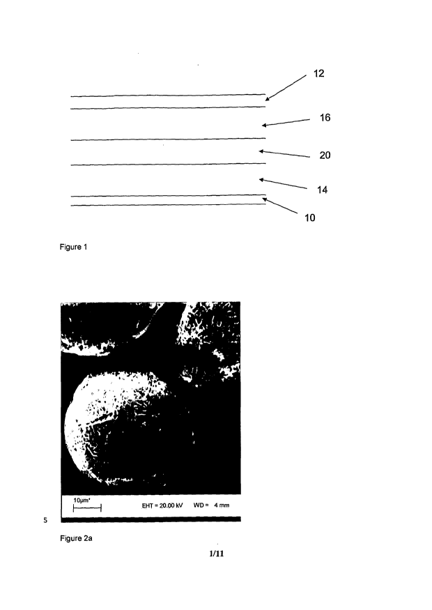
Lithium ion rechargeable batteries are well known. The basic construction of a
lithium ion
rechargeable battery is shown in Figure 1. The battery cell includes a single
cell, but may
include multiple cells.
The battery cell generally comprises a copper current collector 10 for the
anode and an
aluminium current collector 12 for the cathode, which are externally
connectable to a load or
to a recharging source as appropriate. It should be noted that the terms
"anode" and
"cathode" are used in the present specification as those terms are understood
in the context
of batteries placed across a load, i.e. the term "anode" denotes the negative
pole and the
term "cathode" the positive pole of the battery. A graphite-based composite
anode layer 14
overlays the current collector 10 and a lithium containing metal oxide-based
composite
cathode layer 16 overlays the current collector 12. A porous plastic spacer or
separator 20
is provided between the graphite-based composite anode layer 14 and a lithium
containing
metal oxide-based composite cathode layer 16: a liquid electrolyte material is
dispersed
within the porous plastic spacer or separator 20, the composite anode layer 14
and the
composite cathode layer 16. In some cases, the porous plastic spacer or
separator 20 may
be replaced by a polymer electrolyte material and in such cases the polymer
electrolyte
material is present within both the composite anode layer 14 and the composite
cathode
layer 16.
When the battery cell is fully charged, lithium has been transported from the
lithium
containing metal oxide in the cathode via the electrolyte into the graphite-
based anode
where it is intercalated by reacting with the graphite to create a lithium
carbon compound,
typically LiC6. The graphite, being the electrochemically active material in
the composite
anode layer, has a theoretical maximum capacity of 372 mAh/g.
The use of silicon as an active anode material in secondary batteries such as
lithium ion
batteries is well known (see, for example, Insertion Electrode Materials for
Rechargeable
Lithium Batteries, M. Winter, J.O. Besenhard, M.E. Spahr, and P. Novak in Adv.
Mater.
1998, 10, No. 10 and also Wang, Kasavajjula et at, J. Power Source,s 163
(2007) 1003-
1
CA 02810123 2013-03-01
WO 2012/028857
PCT/GB2011/001298
1039). It is generally believed that silicon, when used as an active anode
material in a
lithium-ion rechargeable cell, can provide a significantly higher capacity
than the currently
used graphite anode materials. Silicon, when converted to the compound LivSis
by reaction
with lithium in an electrochemical cell, has a theoretical maximum capacity of
4,200 mAh/g,
considerably higher than the maximum capacity for graphite.
Early approaches of using silicon or silicon based active anode materials in a
lithium ion
electrochemical cell included the use of bulk silicon anodes, silicon powder
anodes
comprising nanometer and micron sized silicon powders, thin film silicon
anodes and silicon
anodes comprising silicon structures other than or in addition to powders.
Composite anodes
comprising a dispersion of silicon in an inactive or active matrix material
have also been
investigated. However, many of the approaches have failed to show sustained or
adequate
capacity over the required number of charge/discharge cycles.
Electrodes comprising bulk silicon failed to exhibit good capacity retention
and cycle-ability
over a number of charging and discharging cycles. This poor performance was
attributed to
the mechanical stresses that arise within the electrode structure during the
charging cycle.
Intercalation or insertion of lithium ions into the bulk silicon structure
during the charging
cycle causes a massive expansion of the silicon containing material, which
leads to a build-
up of mechanical stress within the electrode structure and eventually causes
cracking,
delamination and loss of contact within and between the components of the
electrode
structure and the current collector respectively.
It should be understood that the term "intercalation" when used in relation to
electroactive
materials, particularly the silicon-containing materials, referred to herein
includes a process
where lithium is inserted into and disrupts the structure of the crystalline
or amorphous
silicon-containing material as well as a process in which lithium is dispersed
between crystal
planes defining the silicon-containing structure. The former process is more
properly referred
to as lithium insertion and is observed for materials comprising pure or
substantially pure
crystalline, amorphous and/or polycrystalline silicon. Some compounds or
alloys of silicon
will, however, also exhibit this form of behaviour. The dispersion of lithium
between crystal
planes within a crystalline or polycrystalline silicon-containing material is
more often referred
to as "intercalation" and is usually observed for materials comprising
compounds or alloys of
silicon.
In an attempt to overcome the stresses associated with bulk silicon anodes,
anodes
including silicon structures that are more easily able to accommodate the
volume changes
that occur on charging have been fabricated.
2
CA 02810123 2013-03-01
WO 2012/028857
PCT/GB2011/001298
One of the earlier approaches employed anodes comprising pure silicon powder.
Although it
was expected that anodes fabricated from silicon powder would be better able
to
accommodate the volume expansion associated with lithium intercalation or
insertion
compared to bulk silicon electrodes, it was found that, in practice, these
electrodes fared
little better than bulk silicon electrodes and breakdown of the electronically
conductive
- network due to the expansion of silicon powder particles was also
observed.
In an attempt to improve the electronic contact between anode components
during the
charging and discharging of the cell, composite anodes comprising a mixture of
powdered
silicon and additional components such as a conductive material, a binder and
optionally a
further electroactive material were prepared. It was anticipated that these
further
components would be able to suppress and/or accommodate the large volume
changes
associated with the silicon species during the charging and discharging cycles
of the cell.
However, these electrodes were found to exhibit a reduced capacity compared
with
electrodes comprising silicon only and were unable to maintain this capacity
over a required
number of charging and discharging cycles.
In one prior art approach described by Ohara et al. (Journal of Power Sources
136 (2004)
303-306) which addresses the problems associated with the expansion and
contraction of
silicon during the charging and discharging cycles of the battery, silicon is
evaporated onto a
nickel foil current collector as a thin film and this structure is then used
to form the anode of
a lithium ion cell. However, although this approach gives good capacity
retention, this is the
case for only very thin films and thus the structures do not give usable
amounts of capacity
per unit area and increasing the film thickness to give usable amounts of
capacity per unit
area causes the good capacity retention to be eliminated due to mechanical
breakdown as a
result of the large volume expansion within the film.
Another approach used to address the problems associated with expansion of the
silicon film
is described in US 6,887,511: Silicon is evaporated onto a roughened copper
substrate to
create medium thickness films of up to 10pm. During the initial lithium ion
insertion process
the silicon film breaks up to form columns of silicon. These columns can then
reversibly react
with lithium ions and good capacity retention is achieved. However, the
process does not
function well with thicker films and the creation of the medium thickness film
is an expensive
process. Furthermore the columnar structure caused by the break-up of the film
has no
inherent porosity, which means that over time the pillars will, themselves,
begin to crack and
the electrode structure will likely not exhibit long term capacity retention.
In an attempt to overcome the problems associated with the bulk silicon,
silicon powder and
thin film silicon anodes described above, many workers have investigated
alternative silicon
3
CA 02810123 2013-03-01
WO 2012/028857
PCT/GB2011/001298
and anode structures for the fabrication of anodes for lithium ion batteries.
Examples of
silicon structures investigated include arrays of silicon pillars formed on
wafers and particles;
silicon fibres, rods, tubes or wires; and complete porous particles comprising
silicon. Anode
structures having pores or channels formed therein have also been
investigated.
US 6,334,939 and US 6,514,395 each disclose silicon based nano-structures for
use as
anode materials in lithium ion secondary batteries. Such nano-structures
include cage-like
spherical particles and rods or wires having diameters in the range 1 to 50nm
and lengths in
range 500nm to lOpm. Similar nanostructures are disclosed in KR 1020027017125
and ZL
01814166.8. JP 04035760 discloses silicon based anode materials comprising
carbon-
coated silicon fibres having diameters in the range 10nm to 50pm for use in
lithium ion
secondary batteries. Batteries prepared using these nano-structures exhibited
a total first
cycle charging capacity of 1300 mAh/g and a reversible capacity of 800rnAh/g.
US 2007/0281216 discloses an anode active material for a lithium secondary
battery
comprising a mixture of silicon nano-particles, graphite, carbon black and a
binder. The
silicon nano-particles comprise either thread-like aggregates (a chain of
connected
spheroidal particles) having a primary particle size in the range 20 to 200nm
and a specific
surface area of 11m2/g or spherical particles having a primary particle size
in the range 5 to
50nm and a specific surface area of 170m2/g. The silicon particles and threads
are prepared
using techniques such as chemical vapour deposition. Anodes exhibiting a
capacity of up to
1000mAh/g over 50 cycles are illustrated. The life of the battery is
significantly increased if
the battery is operated at a limited voltage level.
Polycrystalline silicon nano-wires and wires having cross-sectional diameters
in the range 20
to 500nm and aspect ratios of greater than 10, 50 or 100 and which have been
prepared
using epitaxial and non-epitaxial growth techniques are disclosed in US
7,273,732.
Single crystalline silicon fibres, pillars or rods having diameters in the
range 0.1 to 1pm and
lengths in the range 1 to 10pm can also be prepared using lithographic and
etching
techniques as disclosed in US 7,402,829. Alternative etching techniques such
as those
disclosed in WO 2007/083155, WO 2009/010758 and WO 2010/040985 can also be
used.
The fibres, wires and rods described above are typically formed into a
composite material
containing, in addition to the silicon rods, wires and fibres, additional
ingredients such as a
binder, a conductive material and optionally a further electroactive material
other than
silicon. The composite material is also known as an anode mix and is typically
used in the
fabrication of anodes for lithium ion batteries. In accordance with the
disclosure of the
present inventors in WO 2009/010758 and WO 2009/010757 anode materials
comprising
4
CA 02810123 2013-03-01
WO 2012/028857
PCT/GB2011/001298
silicon fibres or rods are preferably in the form of an entangled "felt" or
"mat" in which silicon
fibres are randomly connected with each other either directly or indirectly
through the other
components of the mix, and are also connected with the copper foil which acts
as the current
collector of the electrode.
By the term "felt or mat" it should be understood to mean a structure in which
any one of the
components of the structure is connected in a random or ordered manner with
one or more
other components of the structure so that there are multiple interconnections
between the
components. The mat may be provided in the form of a coating layer which is
directly or
indirectly applied, bonded or connected to a current collector or it may be in
the form of a
self-supporting structure, although this is less preferred. Preferably a felt
or mat comprises
one or more species of fibre as these help to strengthen the overall
structure.
It has been observed by the present inventors that these felt structures
produced using the
silicon rod, wire and fibre products described above have an inherent
porosity, (that is they
contain voids or spaces between the fibres) as a result of the maximum
attainable packing
density of a random arrangement of fibres within a defined volume. These
inherently porous
electrodes were found to exhibit better capacity retention and cycling
lifetimes compared to
electrodes produced from bulk silicon, silicon powders and silicon films, for
example. Without
wishing to be constrained by theory, it is believed that the inherent porosity
of these
electrode structures provides at least some of the silicon components of the
anode with
space to expand into the voids or pores that are part of the electrode
structure rather than
push against each other during lithium intercalation or insertion (charging).
The pores of the
electrode are therefore able to accommodate the expansion of these silicon
components
during lithium intercalation or insertion within the volume initially occupied
by the uncharged
anode material, thereby reducing the volume increase within the electrode
structure, the
build up of stress and the application of pressure on the other cell
components during the
charging and discharging cycle As a result there will be less cracking of the
silicon structures
within the anode and a reduction in the extent of delamination of the
electrode coating from
the current collector, leading to better capacity retention and cycle-ability.
The pores or voids
also facilitate penetration of and therefore contact of the electrolyte with
as much of the
surface of the silicon material as possible during charging and discharging of
the anode. This
porosity is therefore believed to be important as it provides a path by which
the lithium can
be intercalated (or inserted) into the whole of the silicon material so that
the lithiation of the
silicon is as uniform as possible throughout the anode mass.
In addition to using silicon rods and fibres for the fabrication of porous
electrode structures, it
is also known to use silicon components which are themselves porous in the
fabrication of
5
CA 02810123 2013-03-01
WO 2012/028857
PCT/GB2011/001298
porous electrodes or to form holes or channels into silicon based electrode
structures having
minimal porosity.
US 2009/0253033 discloses anode active materials having an inherent porosity
for use in
lithium ion secondary batteries. The anode material comprises silicon or
silicon alloy
particles with dimensions of between 500nm and 20pm and a binder or binder
precursor.
These particles are manufactured using techniques such as vapour deposition,
liquid phase
deposition or spraying techniques. During anode fabrication, the
silicon/binder composite is
heat treated to carbonise or partially carbonise the binder component thereby
providing the
anode with an inherent porosity. In a preferred embodiment the anodes of US
2009/0253033
include pores having dimensions in the range 30nm to 5000nm in order to
accommodate the
expansion of the silicon material during the charging and discharging phases
of the battery.
Anodes prepared using such silicon materials exhibit a capacity retention of
from 70 to 89%
and an expansion coefficient of 1 to 1.3.
Porous silicon anodes created by electrochemically etching channels into a
silicon wafer
have also been prepared. See, for example, HC Shin et al, J. Power Sources 139
(2005)
314-320. Electrolyte penetration was observed for channels having a pore
diameter of 1 to
1.5pm. It was observed that the peak current and the charge transferred during
cyclic
voltammetry increased with channel depth up to a limit. The amount of charge
transferred for
channels having an aspect ratio (channel depth to pore diameter) of the order
of 1 was found
to be only marginally less than those having an aspect ratio of 5. It was
suggested that the
channel walls were able to participate in the lithiation/delithiation and that
the presence of
channels effectively increased the reactive area of the electrode. The porous
structure
remained essentially the same after a number of charge/discharge cycles
despite the
volume changes occurring as a result of the intercalation or insertion and
release of lithium
during these cycles. The channels created by electrochemical etching of a
silicon wafer differ
from the pores or voids created upon formation of a meshed electrode material
using silicon
fibres, wires and rods as described above in WO 2009/101758 and WO
2009/040985. The
electrochemically etched electrode material is rigid and the entire volume of
the electrode
material will expand upon lithium intercalation or insertion. In contrast the
voids within the
meshed electrode material are able to contract and expand in response to the
increase and
decrease in the volume of the mesh comprising silicon components during
lithium
intercalation or insertion and release respectively. This means that silicon
mesh type
electrodes are more able to accommodate volume changes within the electrode
structure
upon lithium intercalation or insertion.
6
CA 02810123 2013-03-01
WO 2012/028857
PCT/GB2011/001298
Rigid electrode structures such as those prepared by Shin et al tend to be
associated with a
build up of stress within the electrode structure on lithium intercalation or
insertion as a result
of the isotropic volume expansion of the entire electrode material. Providing
the voids within
the electrode structure are sufficiently open, the silicon mesh provides
access for the
electrolyte into the bulk of the electroactive anode. In contrast the more
flexible meshed
electrode structures including voids as described above are more able to
accommodate
expansion of the silicon material on lithium intercalation or insertion due
the contraction and
expansion of voids as described above. The overall expansion of a meshed
electrode
structure is therefore significantly less than that of the rigid channelled
electrode structure
described by Shin et al. This means that there will less build up of stress
within meshed
electrode structures compared to rigid electrode structures.
Porous silicon particles are also known and have been investigated for use in
lithium ion
batteries. The cost of manufacturing these particles is believed to be less
than the cost of
manufacturing alternative silicon structures such as silicon fibres, ribbons
or pillared
particles, for example. However, the life cycle performance of many of the
composite
electrodes prepared to date, which comprise porous silicon particles needs to
be significantly
improved before such electrodes could be considered to be commercially viable.
Porous silicon particles having dimensions in the range 4 to 11pm, an average
pore sizes of
6 to 8A and a BET surface area of from 41 to 143m2/g have been prepared for
use in fields
such as drug delivery and explosive design (Subramanian et al, Nanoporous
Silicon Based
Energetic Materials, Vesta Sciences NJ 08852 Kapoor and Redner, US Army RDE-
COM-
ARDEC Picatinny Arsenal NJ 07806, Proceedings of the Army Science Conference
(26th)
Orlando, Florida, 1-4 December 2008). There is no indication in Subramanian et
al that their
silicon containing porous particles would be suitable for use in the
fabrication of lithium ion
batteries.
Silicon nanosponge particles having a network of pores extending through the
particle
structure have also been prepared, US 7,569,202. Nanosponge particles having a
diameter
of 1 to 4pm and pore diameters of 2 to 8nm are prepared by stain etching
metallurgical
grade silicon powders to remove both silicon material and impurities. It is
believed that the
impurities in the metallurgical grade silicon are preferentially etched away
to give particles
having a network of pores distributed throughout. The nanosponge particles can
be surface
treated to introduce functional groups onto the silicon surface. US 7,569,202
teaches that
the surface functional groups enable the nanosponge particles to be used for a
broad range
of applications from drug delivery to explosives. US 7,569,202 does not teach
the application
of nanosponge particles in lithium ion batteries.
7
CA 02810123 2013-03-01
WO 2012/028857
PCT/GB2011/001298
US 7,244,513 discloses a partially porous silicon powder comprising silicon
particles having
a solid silicon core and an outermost layer of porous silicon. These partially
porous silicon
particles are prepared by stain etching particles having a dimension in the
range lpm to
1mm to give partially porous particles having a porous outer shell in which
the pore
dimensions in the range mm to 100nm. The partially porous particles are then
subjected to
ultrasonic agitation to give silicon nanoparticles having a dimension in the
range 10nm to
50nm. US 7,244,513 teaches that the nanoparticles could be used in
applications such as
sensors, floating gate memory devices, display devices and biophysics. There
is no
suggestion that these nanoparticles could be used in the fabrication of a
lithium ion battery.
US 2004/0214085 discloses an anode material comprising an aggregate of porous
particles
that is capable of withstanding pulverization during the charging and
discharging cycles of
the battery. According to US 2004/0214085, the reason why the particles are
able to
withstand pulverisation is because the external volume of the porous particle
is maintained
during the charging and discharging cycle of the battery due to compression of
the particle
voids when the particle expands during the process of intercalating lithium
ions into silicon.
The porous particles in the aggregate have an average particle size in the
range lpm to 100
pm and pore sizes in the range lnm to 10 pm. For particles having diameters of
less than
1pm the relative volume of the pores within the particle is excessive and the
hardness of the
particle is compromised. Particles having a diameter of more than 100pm are
unable to
accommodate the volume changes associated with the intercalation or insertion
and
deintercalation or release of lithium and cannot prevent pulverisation of the
particle. The
particles are prepared by quenching an alloy of silicon with another element,
M to form a
quenched alloy particle comprising an amorphous silicon phase and an element,
M, which
can be eluted from the particle to provide a porous particle. 50:50 and 80:20
silicon-nickel
alloys and 70:30 Al:Si alloys were used to prepare alloy containing particles
using a gas
atomisation technique in which a helium gas pressure of 80kg/cm2 and a
quenching rate of
1x10⁵ K/s was used. The quenched particles were washed in acid (H2SO4 or HCI)
to remove
either the Ni or the Al to give porous particles, which contained a mixture of
both amorphous
and crystalline silicon. Batteries prepared using the Si porous materials of
US 2004/0214085
have a capacity retention of between 83 and 95% over 30 cycles.
The porous particle of US 2004/0214085 is characterised by the ratio of the
pore diameter,
n, to the particle diameter, N and the volume ratio of the voids to the porous
particle. n/N is
preferably in the range 0.001 to 0.2 so that the diameter of the pores within
the particles is
very small in order that the hardness of the particle can be maintained. The
volume ratio of
the voids to the porous particle is preferably in the ratio 0.1% to 80% so
that the expansion
and contraction of the silicon volume during intercalation or insertion and
deintercalation or
8
CA 02810123 2013-03-01
WO 2012/028857
PCT/GB2011/001298
releaseof lithium is fully compensated by the voids, the entire volume of the
porous particle
is maintained and the particles are not degenerated.
US 7,581,086 discloses an electrode material comprising porous silicon
particles, which
particles are prepared by quenching a eutectic alloy of silicon and another
metal (typically
aluminium) using a roll solidification method at a cooling rate of greater
than 100K/s to give a
thin film alloy sheet. The thin film is pulverised to give alloy particles
having a typical
diameter of 15pm, which are typically etched in HCI to give porous Si
particles. Electrode
materials prepared from these powder particles exhibited a capacity retention
of
approximately 68% at 10 cycles.
US 2009/0186267 discloses an anode material for a lithium ion battery, the
anode material
comprising porous silicon particles dispersed in a conductive matrix. The
porous silicon
particles have a diameter in the range 1 to 10pm, pore diameters in the range
Ito 100nm
(preferably 5nm), a BET surface area value in the range 140 to 250m2/g and
crystallite sizes
in the range 1 to 20nm. The porous silicon particles are mixed with a
conductive material
such as carbon black and a binder such as PVDF to form an electrode material,
which can
be applied to a current collector (such as a copper foil) to give an
electrode. Although US
2009/0186267 suggests that these materials could be used for the manufacture
of a battery,
there is no data in this document to suggest that a battery has actually been
manufactured.
Kim et al teaches the preparation of three-dimensional porous silicon
particles for use in high
performance Jithium secondary batteries in Angewandte Chemie Int. Ed. 2008,
47, 10151-
10154. Porous silicon particles are prepared by thermally annealing composites
of butyl
capped silicon gels and silica (Si02) nano-particles at 900 C under an argon
atmosphere
and etching the silica particles out of the annealed product to give a carbon
coated porous
amorphous silicon particle having a pore wall thickness of 40nm, pore
diameters of the order
of 200nm and an overall particle size of greater than 20pm. Silicon
crystallites having a
diameter of less than 5nm were observed within the structure. Half cells
prepared using
these amorphous porous particles exhibited improved first cycling efficiency,
which was
thought to be due to the carbon coating. It was also suggested that an
amorphous silicon
structure could act as a buffer against the expansion of crystalline silicon
upon intercalation
or insertion.
Although anode structures comprising silicon fibres, rods and wires have been
found to
exhibit both a better capacity retention and an improved cycle life compared
to bulk silicon
and silicon powder anodes, an improvement in their absolute capacity and cycle
life is still
desired. Depending on the shape and dimension of the silicon elements, there
can be a limit
to the achievable packing density in the composite mix which can restrict the
maximum
9
CA 02810123 2013-03-01
WO 2012/028857
PCT/GB2011/001298
achievable electrode capacity. Furthermore, the methods and costs associated
with the
manufacture of these silicon structures needs to be further refined and
reduced respectively.
Even with inherent porosity, electrode structures comprising silicon fibres,
rods and wires
have been observed to exhibit an effect known as "heave" in which the bulk of
the silicon
electrode material expands away from the surface current collector during
intercalation,
which may result in delamination. This bulk does appear to survive the heave
process and is
able to substantially resume its original configuration on release of the
lithium from the
silicon fibres, but it exerts pressure on other cell components during
cycling.
Further it has been found to be difficult to prepare anode structures
comprising porous
silicon particles that are able to provide adequate performance in terms of
absolute capacity,
capacity retention and cycle-ability. Anode structures comprising porous
particles of
diameter less than 500nm, for example, do not exhibit good capacity
characteristics because
the particle pores are generally too small to facilitate electrolyte
penetration and efficient
intercalation or insertion and release of lithium into the silicon structure.
Further, the small
particles tend to agglomerate within the electrode structure, which leads to
delamination over
a number of charging and discharging cycles. In addition because the pore wall
thickness
(average thickness of material separating any one void or pore within a
particle structure
from its adjacent pore or void) of these particles tends to be very low (less
than 50nm), their
associated surface area tends to be high. A high surface area is associated
with significant
first cycle losses of lithium in the electrode structure due to the formation
of an excessive
Solid Electrolyte Interphase layer (SEI) as a result of the consumption of
lithium in the
formation of these layers. Particles containing pores of a sufficiently large
size to
accommodate electrolyte penetration and which have thicker pore walls of 0.1
to 2pm tend
themselves to have diameters that are too large to be successfully
accommodated into an
electrode structure having an overall uniform thickness of around 50pm.
The fibres or wires used in the formation of silicon mesh electrode structures
are also
believed to have a high surface area to volume ratio. These mesh like
electrode structures
are also believed to be associated with high first cycle losses for the
reasons given above.
It will be appreciated from the foregoing that the majority of approaches used
to date for
creating porous particles result in the production of approximately spheroidal-
shaped
particles with relatively smooth curved surfaces. Such shapes are not ideal
for creating
networks of electronically connected particles in an electrode. This is
because the surface
area of contact between one spheroidal particle and another or between one
spheroidal
particle and a conductive additive particle is small; this means that the
electronic conductivity
throughout the connected mass of active particles is relatively low, reducing
performance.
CA 02810123 2013-03-01
WO 2012/028857
PCT/GB2011/001298
Many of the electrodes produced using the electro-active silicon materials
discussed herein
above are not able to exhibit the characteristics of uniform thickness,
homogeneity and
porosity. Such electrodes do not comprise a strongly connected network of
active particles
that are able to accommodate the expansion and contraction of the silicon
material into its
own volume without cracking or de-lamination during the charging cycles of the
battery.
There is a need, therefore, for an electroactive material and an electrode
structure that
addresses the problems associated with the silicon based electrodes outlined
above.
2. Compositions Comprising Porous Particle Fragments
A first aspect of the invention provides a composition comprising a plurality
of electroactive
porous particle fragments comprising an electroactive material selected from
the group
comprising silicon, tin, germanium, gallium, aluminium and lead. Preferably
the porous
particle fragments comprise silicon (which will hereafter also be referred to
as silicon
containing porous particle fragments). By the term "porous particle" it should
be understood
to include a particle comprising a plurality of pores, voids or channels
within a particle
structure, wherein each of the pores, voids or channels within the particle
structure is
defined, bound, partially bound or separated by the electroactive material
from which the
particle is formed. The term "porous particle" should also be understood to
include a
particulate material comprising a random or ordered network of linear,
branched or layered
elongate elements, wherein one or more discrete or interconnected void spaces
or channels
are defined between the elongate elements of the network; the elongate
elements suitably
include linear, branched or layered fibres, tubes, wires, pillars, rods,
ribbons or flakes.
Layered elongate elements include structures in which the elongate elements
are fused
together. The individual branched elongate elements typically have a smallest
dimension in
the range 50 to 100nm with branches every 100 to 400nm. The porous particles
from which
the porous particle fragments are derived can further be defined in terms of a
smallest
dimension (or pore wall thickness), this being the average thickness of
material separating
any one pore or void within a pore containing porous particle structure from
an adjacent void,
or where the particle comprises a network of elongate elements, the average
thickness (this
being the average smallest dimension) of an elongate element within the
network. By the
term porous particle fragment it should be understood to include all fragments
derived from a
porous particle, preferably a porous particle formed from an electroactive
material such as
silicon, tin, germanium, gallium, aluminium and lead. Silicon containing
porous particles are
especially preferred. Such fragments include structures having a substantially
irregular
shape and surface morphology, these structures being derived from the
electroactive
material originally defining, bounding, partially bounding or separating the
pores or network
11
CA 02810123 2013-03-01
WO 2012/028857
PCT/GB2011/001298
of pores within the porous particle from which the fragment structures are
derived, without
themselves comprising pores, channels or a network of pores or channels.
Preferably these
fragments are derived from the electroactive material, preferably the silicon
material either
(a) defining the network of elongate elements or (b) originally defining
bounding, partially
bounding or separating the pores or network of pores within the porous
particle from which
the fragment structures are derived, without the fragments themselves
comprising pores,
channels or a network of pores or channels. These fragments will hereafter be
referred to as
fractals. The appearance of the fractals may or may not resemble the porous
particles from
which they are derived. Typically the term 'fractal" as described herein
describes a structure
obtained through the random fragmentation of a larger porous particle. The
surface
morphology of these fractal structures (which are devoid of pores or channels
or a network
of pores or channels) may include an ordered or disordered array of
indentations or
irregularities arising from the pores or channels or network of pores or
channels originally
bound or partially bound by the electroactive material structure, preferably
the silicon
structure of the parent porous particle. These fractal fragments will
typically be characterised
by the presence of peaks and troughs extending over the surface thereof and
will include
particles having a spiky appearance as well as those including a plurality of
ridges or bumps
extending from the surface of the particle. The peaks are characterised by a
peak height and
a peak width. The peak height is defined as the distance between the base of
the peak (the
place where the peak merges with the body of the fractal) and the apex of the
peak. The
peak width is defined as the minimum distance between one side of the peak and
the other
at half height. The fractal can also be defined by the average thickness of
the fractal body;
this value is typically identical to the average thickness (smallest
dimension) of an elongate
element derived from a porous particle comprising a network of elongate
elements or the
average thickness (preferably the pore wall thickness) of the electroactive
material originally
separating any two adjacent pores within the pore containing porous particle
from which the
fractal is derived.
The term porous particle fragment also includes porous particle fragments
comprising a
network of pores and/or channels defined and separated by the electroactive
material
defining the walls of the particle. Pore-containing porous particle fragments
can also be
defined in terms of the average thickness of the electroactive material
separating two
adjacent pore structures within the parent particle (also referred to herein
as the pore wall
thickness). Preferably the electroactive material is a silicon containing
electroactive material
and the term "silicon-containing electroactive material" should be interpreted
to include
electroactive materials comprising essentially substantially pure or
metallurgical grade
silicon, alloys of silicon with both electroactive and non-electroactive
elements as well as
12
CA 02810123 2013-03-01
WO 2012/028857
PCT/GB2011/001298
materials comprising electroactive compounds of silicon. Suitable silicon
alloys include alloys
of silicon with one or more metallic elements selected from aluminium, copper,
titanium,
strontium, nickel, iron, antimony, chromium, cobalt, tin, gold, silver,
beryllium, molybdenum,
zirconium and vanadium. These fragments will herein after be referred to as
pore containing
fragments. By the term "pore" or "channel" as defined in relation to the
particles from which
the fragments are derived as well as the porous particle fragments themselves,
it should be
understood to mean a void or channel enclosed or partially enclosed within the
total volume
of the particle as well as a channel extending into the interior of the
particle from its surface.
These pore and/or channel comprising porous particle fragments are also
generally but not
exclusively characterised by an irregular shape and surface morphology. In
contrast, the
particles from which the fragments are derived are generally but not
exclusively
characterised by a disc-like or substantially spherical shape and a relatively
smooth outer
surface morphology (inbetween the surface voids). Where the fractals and pore
containing
porous particle fragments are described together hereinafter they will
collectively be referred
to as either porous particle fragments or silicon containing porous particle
fragments as
appropriate. The network of pores and/or channels suitably comprises a three
dimensional
arrangement of pores and/or channels extending through the volume of the
particle in which
the pore and/or channel openings are provided on two or more planes over the
surface of
the pore containing porous particle fragment.
As indicated above, the porous particle fragments comprising the composition
of the first
aspect of the invention suitably comprise an electroactive material selected
from the group
silicon, tin, germanium, gallium, aluminium and lead and mixtures thereof as
well as alloys of
these elements with each other and/or with other electroactive or non-
electroactive
elements, providing the composition still exhibits electroactive properties.
Silicon-containing
electroactive materials are preferred. The silicon-containing porous particle
fragments may
be in the form of an alloy with or include additives such as Al, Sb, Cu, Mg,
Zn, Mn, Cr, Co,
Ti, V, Mo, Ni, Be, Zr, Fe, Na, Sr and P. Preferably the electroactive material
is silicon, tin,
aluminium or gallium. More preferably the electroactive material is an alloy
of silicon and
aluminium. Porous particle fragments comprising silicon or a silicon aluminium
alloy are
especially preferred. Porous silicon particle fragments prepared from porous
particles, which
porous particles were formed by etching particles of an aluminium silicon
alloy comprising
from 11 to 30wt% silicon, for example 12w1%, 26wt%, 27wt% and 30wt% silicon
and
fabricated using either a gas atomisation or melt spinning technique are
especially preferred.
The nature of the porous particles will in turn depend upon the technique used
to fabricate
the alloy particles and the processing conditions employed, the composition of
the alloy and
the particle size of the alloy droplets. Fragments prepared from porous
particles formed by
13
CA 02810123 2013-03-01
WO 2012/028857
PCT/GB2011/001298
etching alloy particles of diameter less than 90pm made using a gas
atomisation technique
and comprising up to 12wt% silicon are characterised by a network of fine
silicon structures
having a fractal thickness of from 50 to 100nm. Fragments prepared by etching
alloy
particles of diameter 90 to 1500pm formed using either the gas atomisation
technique or the
melt spinning technique and comprising up to 12wt% silicon are characterised
by a coarser
network of silicon structures having a fractal thickness of from 100 to 200nm.
Fragments
prepared by etching alloy particles of a similar diameter but containing a
hypereutectic
concentration of silicon, e.g. 12 to 30wt% silicon, have similar dimensional
characteristics
but with the addition of low aspect ratio crystalline silicon particles with
typical dimensions of
1-3pm. Compositions comprising silicon structures having a fractal thickness
of from 100 to
200nm are particularly preferred. The invention will hereafter be described
with reference to
electroactive materials comprising silicon and alloys thereof and will
typically be referred to
as silicon-containing porous particles fragments. It should, however, be
appreciated that
although silicon-containing porous particle fragments as described herein
above are
especially preferred, the present invention extends to porous particle
fragments comprising
alternative electroactive materials such as tin, germanium, gallium, aluminium
and lead and
the term "silicon-containing" should be interpreted to extend in the context
of the present
invention to electroactive materials comprising tin, germanium, gallium,
aluminium and lead.
The composition of the first aspect of the invention is an electroactive
material that is able to
form an alloy with lithium (either by insertion and/or by intercalation) and
which can also be
used in the fabrication of anodes for use in lithium ion secondary batteries
or batteries based
around alternative ions as the charge carrier, for example alkali metal ions
such as sodium
or potassium ions or magnesium ion batteries. By the term "electroactive
material" it should
be understood to mean that the material is able to accommodate and release
lithium or other
alkali metal ions, or magnesium ions into or from its structure during the
charging and
discharging cycles of a battery.
Suitably the composition according to the first aspect of the invention is
provided in the form
of an electrode material, preferably a composite electrode material, which is
connected or
applied to a current collector and used in the manufacture of an electrode. By
the term
"electrode material" it should be understood to mean a material comprising an
electroactive
material, which can be applied, bonded, adhered or connected to a current
collector. By the
term "composite electrode material" it should be understood to mean a material
comprising a
mixture, preferably a substantially homogeneous mixture, of an electroactive
material, a
binder and optionally one or more further ingredients selected from the group
comprising a
conductive material, a viscosity adjuster, a cross-linking accelerator, a
coupling agent and an
adhesive accelerator. The components of the composite material are suitably
mixed
14
CA 02810123 2014-01-07
together to form a homogeneous composite electrode material that can be
applied as a coating
to a substrate or current collector to form a composite electrode layer.
Preferably the
components of the composite electrode material are mixed with a solvent to
form an electrode
mix, which electrode mix can then be applied to a substrate or current
collector and dried to
form the composite electrode material.
In accordance with one aspect of the invention there is provided a composition
comprising
silicon containing electroactive porous particle fragments, wherein the porous
particle
fragments are selected from the group consisting of:
a. A pore-containing porous particle fragment comprising a network of pores,
cavities and channels, which pores, cavities and channels are separated and
defined
by silicon-containing walls within the particle structure;
b. A fractal comprising a substantially irregular shape or surface morphology
derived
from the silicon material originally defining or bounding the pores or network
of
pores within the porous particle from which the fractals are derived without
themselves comprising pores, channels or a network of pores or channels; and
c. A fractal having a substantially irregular shape or surface morphology
derived from
silicon material originally defining a random or ordered network of linear,
branched
or layered elongate elements, wherein one or more discrete or interconnected
void
spaces or channels are defined between the elongate elements of the network.
By the term "electrode mix" it should be understood to mean compositions
including a slurry or
dispersion of an electroactive material in a solution of a binder as a carrier
or solvent. It
should also be understood to mean a slurry or dispersion of an electroactive
material and a
binder in a solvent or liquid carrier.
Further the term "composite electrode" should, in the context of the present
invention, be
understood to mean an electrode structure comprising a current collector
having an
electroactive material or a composite electrode material applied, bonded,
adhered or connected
thereto. The current collector may be provided in the form of a sheet or a
mesh. The
electroactive material may be in the form of a coating applied thereto. The
coating may be
provided in the form of a felt or a mat, the felt or mat being applied,
bonded, adhered or
connected to the current collector.
In a first preferred embodiment of the first aspect of the invention, the
silicon containing
porous particle fragments are fractals. Without wishing to be constrained by
theory, it is
believed that composite electrodes comprising fractals are associated with a
greater capacity,
improved cycle-ability (cycling characteristics) and an optimum porosity
compared to bulk
CA 02810123 2014-01-07
silicon and silicon powder composite electrodes, for example. The fractals are
believed to pack
together more closely within the electrode structure compared to non-
fragmented spherical
particles. This close packing is believed to contribute to an improved
capacity. The irregular
surface morphology of the fractals is believed to contribute to both improved
connectivity and
improved porosity within the electrode structure. The presence of peaks on the
surface of the
fractals provides contact points on each fractal surface for connection to
other electroactive
and conductive components within an electrode mix. In addition, the irregular
surface
morphology means that a number of voids will be created within the electrode
structure as a
result of the incomplete overlap of the fractals either with each other or
with the other
components of the electrode structure with which they are packed.
It has been found that the structure of the fractal material depends on the
structure of the
porous particle from which it is derived (parent porous particle). The
structure of the parent
porous particle depends upon the composition of the material from which it is
formed and the
method of formation. If the parent porous particles are prepared from alloy
particles, such as
15a
CA 02810123 2013-03-01
WO 2012/028857
PCT/GB2011/001298
a silicon aluminium alloy, the particle structure will depend on both the
alloy composition and
the method used to form the alloy particle. Cooling techniques (and variations
of the cooling
rates employed in the techniques) such as gas atomisation techniques and melt
spinning
techniques can be used to form alloy particles of different dimensions and
morphologies.
The range of achievable cooling rates will vary with each technique. In
general, faster
cooling rates will tend to produce finer morphologies in the final fractal
material though the
overall size of the alloy particles can also have an effect. The use of the
gas atomisation
technique typically produces particles having finer morphologies that those
produced using
melt spinning. Finer morphologies are also observed in alloy particles
prepared from eutectic
alloy compositions compared to hypereutectic compositions.
Compositions having fine silicon structures (fractal thickness of 50 to 100nm)
were prepared
by cooling silicon aluminium alloys comprising 12wt% silicon using a gas
atomisation
technique and selecting the alloy particles having a diameter of 10pm to 90pm
for etching to
form the porous particles. Coarser silicon structures (fractal thickness of
100 to 200nm) were
prepared by either cooling silicon aluminium alloys comprising 12wt% silicon
using a gas
atomisation technique and selecting the alloy particles having a diameter in
the range 90 to
1500pm or through the use of a melt spinning technique.
Coarser silicon structures having a fractal thickness of from 100nm to 200nm
were also
prepared by cooling silicon aluminium alloys comprising 27 to 30wt% silicon
using either a
gas atomisation or melt spinning technique.
The dimensions of the silicon containing porous particle fragments suitability
facilitate their
accommodation into an anode having an active layer thickness (excluding any
current
collector or supporting substrate) of the order of 40pm, without compromising
the anode
structure and capacity. Because the silicon containing porous particle
fragments are
relatively small, they are inherently suitable for use in the preparation of a
homogenous
electrode or anode material that can be used to provide a smooth and
continuous electrode
coating or mat.
2.2 Characteristics of Porous Particle Fragments
As indicated above, the porous particle fragments according to the first
aspect of the
invention are suitably characterised by an average pore wall or fractal
thickness of between
50nm and 2pm, preferably 100nm to 1pm, especially 100nm to 200nm. Suitably
porous
particle fragments having a pore wall or fractal thickness in the range 50nm
to 2pm,
preferably 100nm to 1pm, especially 100nm to 200nm comprise at least 10% of
the volume
of the porous particle fragments used in the composition of the first aspect
of the invention.
16
CA 02810123 2013-03-01
WO 2012/028857
PCT/GB2011/001298
Preferably porous particle fragments having a pore wall or fractal thickness
in the range
50nm to 2pm, preferably 100nm to 1pm, especially 100nm to 200nm comprise at
least 30%
of the volume of the porous particle fragments used in the composition of the
first aspect of
the invention. More preferably porous particle fragments having a pore wall or
fractal
thickness in the range 50nm to 2pm, preferably 100nm to 1pm, especially 100nm
to 200nm
comprise at least 50% of the volume of the porous particle fragments used in
the
composition of the first aspect of the invention. Most preferably porous
particle fragments
having a pore wall or fractal thickness in the range 50nm to 2pm, preferably
100nm to 1pm,
especially 100nm to 200nm comprise at least 70% of the volume of the porous
particle
fragments used in the composition of the first aspect of the invention. It is
especially
preferred that porous particle fragments having a pore wall or fractal
thickness in the range
50nm to 2pm, preferably 100nm to 1pm, especially 100nm to 200nm comprise at
least 90%
of the volume of the porous particle fragments used in the composition of the
first aspect of
the invention. In a most preferred embodiment of the first aspect of the
invention porous
particle fragments having a pore wall or fractal thickness in the range 50nm
to 2pm,
preferably 100nm to 1pm, especially 100nm to 200nm comprise 10 to 100% of the
volume of
the porous particle fragments used in the composition of the first aspect of
the invention,
preferably 30 to 100%, more preferably 50 to 90% and especially 70 to 90%.
The size of the particle fragments is suitably determined using laser
diffraction techniques
that can be carried out using instruments such as the Malvem Master SizerTm.
Such
techniques are well known to a skilled person. Laser diffraction calculates
the equivalent
diameter of a sphere having the same volume as a non-spherical particle and
provides a
volume distribution of the particles within a sample. Alternative techniques
that can be used
to measure size distributions include digital imaging and processing such as
Malvem
MorphologiTM where the diameter of a sphere or ellipse of a particle of the
same projected
cross-sectional area of the particle being measured is calculated and a number
or volume
distribution of a sample can be provided. The pore sizes of the pore
containing porous
particle fragments suitably accommodates both the expansion of the pore wall
on
intercalation or insertion of silicon and the penetration of electrolyte
during the charging and
discharging cycles of the battery. The thickness of the fractal material and
that of the pore
walls for both the fractals and pore containing porous particle fragments
respectively is
believed to be an important parameter in the context of the present invention
and needs to
be sufficient to impart to the anode structure, of which it forms a part,
enough capacity to
reversibly intercalate and release lithium. The pore wall thickness and the
thickness of the
fractal material must not be too thin as this would lead to excessive lithium
loss due to the
formation of an SEI layer and high first cycle losses. However, the fractal
material and that of
17
CA 02810123 2013-03-01
WO 2012/028857
PCT/GB2011/001298
the pore walls must not be too thick as this would lead to a build-up of
stress within the
structure, which can cause the particle to crumble, and an increased
resistance to the
passage of ions into the bulk of the silicon. In this respect, the facile
fabrication of a good
quality homogeneous coating or mat requires the use of silicon containing
porous fragments
having a maximum overall dimension in the range 1 to 40pm, preferably 1 to
20pm and
especially 3 to 10pm. Porous particle fragments having diameters of less than
50nm are less
preferred as particles of this size tend to agglomerate, which results in the
formation of an
inhomogeneous mat or coating. Suitably porous particle fragments having a
maximum
overall dimension in the range 1 to 40pm, preferably 1 to 20pm and especially
3 to 10pm
comprise at least 10% of the volume of the porous particle fragments used in
the
composition of the first aspect of the invention. Preferably porous particle
fragments having a
maximum overall dimension in the range 1 to 40pm, preferably 1 to 20pm and
especially 3 to
10pm comprise at least 30% of the volume of the porous particle fragments used
in the
composition of the first aspect of the invention. More preferably porous
particle fragments
having a maximum overall dimension in the range 1 to 40pm, preferably 1 to
20prn and
especially 3 to 10pm comprise at least 50% of the volume of the porous
particle fragments
used in the composition of the first aspect of the invention. It is especially
preferred that
porous particle fragments having a maximum overall dimension in the range 1 to
40pm,
preferably 1 to 20pm and especially 3 to 10pm comprise at least 70% of the
volume of the
porous particle fragments used in the composition of the first aspect of the
invention. Where
the silicon containing porous particle fragment is a pore containing fragment,
each pore
containing fragment comprises a three dimensional arrangement of pores having
pore
diameters in the range 60nm to 10pm, preferably 100nm to 5pm and especially
150nm to
2pm. The fractal material and the walls separating the pores within the porous
particle
fragments suitably have a thickness in the range 0.05 to 2pm, preferably 0.1
to 1pm,
especially 100nm to 200nm.
Typically the ratio of pore diameter to wall thickness for pore containing
fragments is suitably
greater than 2.5:1 and is preferably in the range 3:1 to 25:1. The ratio of
the volume of the
pores to the volume of the fragment (otherwise known as particle porosity) is
suitably in the
range 0.2 to 0.8, preferably 0.25 to 0.75 and especially 0.3 to 0.7.
The porous particle fragments suitably have a BET surface area of greater than
0.5 m2/g,
preferably at least 5m2/g. A higher surface area improves the electrical
connectivity and
ionic reactivity of the fragments as the active material in an electrode and
generally
increases the rate at which lithium can be inserted into the silicon. However
a higher surface
area leads to a larger amount of SEI layer being formed during charge and
discharge of the
electrode and consequently a higher lithium loss and reduced cycle life of the
18
CA 02810123 2013-03-01
WO 2012/028857
PCT/GB2011/001298
electrochemical cell. Therefore a suitable balance needs to be made between
these
competing effects. Accordingly, preferably the porous particle fragments have
a surface area
of less than 50m2/g , more preferably less than 30m2/g. Preferred porous
particle fragments
having a BET surface area in the range 4 to 50m2/g, more preferably 4 to
40m2/g, especially
5 to 30m2/g. Silicon structures prepared from melt spun 12w60 Si-Al alloy were
found to
have a BET surface area in the range 10.51 to 15.97m2/g. Silicon structures
prepared from
around 90-1500pm alloy particles prepared by gas atomisation of a silicon
aluminium alloy
comprising 12wt% silicon and having a fractal thickness of 100 to 200nm are
typically
characterised by a BET surface area of 7 to 22m2/g. However finer silicon
structures
prepared from 10-90pm alloy particles prepared by gas atomisation of a silicon
aluminium
alloy comprising 12wt% silicon typically have a higher BET for example in the
region of 40 to
70m2/g, depending on the mix of the alloy particle dimensions in the measured
sample. BET
values around the upper end of this range are less preferred. Silicon
structures prepared
from alloy particles prepared by gas atomisation of a silicon aluminium alloy
comprising
30wt% silicon and having a fractal thickness of 100 to 200nm are typically
characterised by a
BET surface area of 10 to 15m2/g.Pore diameters and BET surface area values
for pore
containing porous particle fragments and fractals can be measured using both
mercury and
gas adsorption porosimetry techniques that are well known to a person skilled
in the art.
Mercury porosimetry can be used to determine the pore size distribution, the
pore volume,
the pore area and porosity of both a meso-porous (pore size of between 2 to
50nm) and a
macro-porous (pore size of greater than 50nm) sample. Gas adsorption
porosimetry (using
gases such as helium, argon or nitrogen, preferably nitrogen) can be used to
determine the
specific surface area and porosity of micro-porous sample (down to pore size
of 2nm or
less). The specific surface area and porosity of compositions comprising
porous particle
fragments according to the first aspect of the invention can suitably be
measured using
mercury porosimetry techniques.
The porosity of the particle should be distinguished from the porosity of the
composition of
the first aspect of the invention. Particle porosity is (as indicated above)
defined by the ratio
of the volume of the pores to the total volume of the particle. Where the
porous particle
fragments are prepared by alloy etching, the particle porosity can most easily
be determined
by knowing the density of the alloy particle from the compositional ratios and
comparing the
mass of a sample before and after the etching and partial crushing steps, if
all the metal
matrix (e.g. aluminium) material is removed during etching. Tap density
measurements
before and after etching can also provide comparative values of particle
porosity. The
composition porosity can be defined as the ratio of the volume of voids in the
composition to
the total volume of the composition and is the sum of both the particle
porosity and the
19
CA 02810123 2013-03-01
WO 2012/028857
PCT/GB2011/001298
packing density of the porous particle fragments and other elements within the
composition.
Where the composition comprises fractals only, the composition porosity
defines the bulk
porosity of the fractals per se; the fractals do not have significant inherent
porosity.
The silicon containing porous particle fragments can further be characterised
by one or more
parameters including bulk resistivity, powder resistivity, Seebeck
Coefficient, and the 111
plane lattice spacing and crystallite size of the silicon crystallites within
the silicon material as
measured by X-ray diffraction spectrometry.
The Seebeck Coefficient of the porous particle fragments or fractals can be
measured by
placing a sample of the particle fragments in a circular pressure cell of
approximate
lo dimensions 5 mm diameter by 5mm thick and applying a pressure of 40MPa.
A small
temperature gradient is then formed across the thickness direction of the cell
using a heater
in the cell base. Measurement of the resulting thermal voltage generated
across the cell
thickness provides the Seebeck Coefficient, S, in V/K at room temperature
(e.g. 21 deg C).
For a material such as silicon, the Seebeck Coefficient is dependent on the
carrier density,
i.e. the number of free electrons or holes with the silicon. The sign of S
depends on the type
of the majority carrier ¨ it is positive for p-type (holes) and negative for n-
type (electrons). A
smaller magnitude of S relates to a higher carrier density indicating a higher
level of doping
and a higher conductivity. For the active material of a electrochemical cell
electrode, a higher
conductivity and therefore, a lower value of S is preferred. Preferably the
absolute
magnitude of S (at room temperature, ISI) is less than 300pV/K, more
preferably less than
250pv/k and especially less than 100pV/K. The method of making porous particle
fragments
described herein where a molten alloy comprising an active material and a
metal matrix
material is rapidly quenched to form alloy particles from which the metal
matrix material is
removed by etching, is particularly advantageous in producing an active
material with a low
Seebeck Coefficient (plus a high level of doping and low resistivity) when the
metal matrix
material in the alloy comprises a doping element of the active material.
Making porous
particle fragments from Al-Si alloy particles is preferred because aluminium
is a p-type
dopant for silicon and this produces a very highly doped silicon material
which is believed to
be beneficial for electrode performance without the need for any additional
doping process
step.
Where the silicon containing porous particle fragments are characterised in
terms of their
resistivity, this is value may be determined for a bulk sample (suitably, but
not exclusively, a
sintered bulk sample) including these materials. Suitably a bulk sample of the
porous particle
fragments has a resistivity of less than 100/cm, preferably less than 1 0/cm,
more preferably
less than 0.10./cm and especially less than 0.010/cm.
CA 02810123 2013-03-01
WO 2012/028857
PCT/GB2011/001298
The bulk resistivity of the silicon porous particle fragments can also be
estimated from the
measurement of the Seebeck Coefficient, S. A suitable method is as follows:
the carrier
density, p, is calculated using the equation S = (k/q)*(2.5 ¨ In(p/Nv)) where
Nv=1.8x10¹⁹/cm3,
k is Boltzmann's constant (1.38065 x 10⁻²³ J/K) and q is the elementary charge
of an electron
(1.602176 x 10⁻¹⁹ C). Using the calculated value of the carrier density, the
resistivity can be
estimated using one of the methods described in ASTM Standard F723-99 using
the
assumptions that the dopant density is equal to the carrier density and the
conversion
factors given in ASTM F723-99 for boron doped silicon can be used for
aluminium doped
silicon. For the calculations given herein, the graphical method for boron
doped silicon using
the resistivity-dopant density conversion from Thurber et al., NBS special
Publication 400-64
(April 1981), as described in ASTM F723-99, is used.
The tap density refers to the bulk density of a powder comprising porous
particle fragments
after a specified compaction process, usually involving vibration of container
holding a
sample of the powder. For a bulk sample comprising porous particle fragments
typical tap
densities after 6000 taps are in the range of 0.1 to 0.6 g/cm3.
X-ray diffraction spectrometry analysis provides an indication regarding the
crystallinity and
average crystallite size of a sample. X-ray diffraction spectrometry analysis
(using an X-ray
wavelength of 1.5456nm) of the porous particle fragments of the present
invention indicates
that the fragments comprise a polycrystalline material having a crystallite
size of between 45
and 55nm with a crystal plane 111 lattice spacing of between 3.14 and 3.16A.
The crystallite
size is calculated using the Scherrer equation where the shape constant K is
taken to be
0.94. Silicon material prepared from a gas atomised 12wt% silicon aluminium
alloy particles
of size 10-90pm (that typically produce finer particle fragments with higher
BET values) is
typically characterised by a crystallite size of 51nm and a crystal plane 111
lattice spacing of
3.156A. Silicon material prepared from gas atomised or melt spun 12wt% silicon
aluminium
alloy particles of size 90 to 1500pm (that typically produce coarser particle
fragments with
lower BET values) is typically characterised by a crystallite size of 45.5nm
and a crystal
plane 111 lattice spacing of 3.145k Silicon material prepared from a melt spun
30wt%
silicon aluminium alloy that also typically produces coarser particle
fragments with lower BET
values is typically characterised by a crystallite size of 49.2nm and a
crystal plane 111 lattice
spacing of 3.142A. The silicon material with a 111 lattice spacing of less
than 1.5 A is
preferred. It would appear that the porous particle fragments prepared from
rapidly cooling
and then etching silicon aluminium alloys comprising from 12 to 30wt% possess
significant
crystallinity. Porous particle fragments with a crystallite size of at least
20nm are preferred,
more preferably at least 30nm.
21
CA 02810123 2013-03-01
WO 2012/028857
PCT/GB2011/001298
2.2.1 Characterisation of Parent Porous Particles
As indicated, the silicon containing porous particle fragments of the
composition of the first
aspect of the invention are suitably derived from larger porous particles
(including porous
particles comprising a network of elongate elements) having a diameter in
excess of 40pm,
.. preferably at least 60pm and more preferably at least 100pm. Porous
particles having
diameters up to 1000pm or 1500pm can also be used to prepare the porous
particle
fragments according to the first aspect of the invention. Preferably the
porous particle
fragments are derived from porous particles (including porous particles
comprising a network
of elongate elements) having a diameter in the range 40 to 200pm, preferably
60 to 80pm,
.. more preferably 70 to 150pm and especially 100 to 150pm. Preferably the
porous particle
fragments of the first aspect of the invention are prepared from porous
particles (including
porous particles comprising a network of elongate elements) having a diameter
in the range
60 to 1500pm, more preferably 150 to 1000pm. Preferably the fragments are
derived from
spheroidal and non-spheroidal-based larger porous particles (including porous
particles
.. comprising a network of elongate elements) and have, themselves, an
essentially non-
spheroidal shape with one or more surfaces of low curvature. Preferably the
fragments have
an average smallest dimension (pore wall thickness or elongate element
thickness) which is
less than half the value of the largest dimension (usually length). It has
been found that
anodes prepared using particle fragments of the type and dimensions specified
above, which
.. themselves have been derived from larger porous particles having a diameter
specified
above exhibit improved capacity and cycling characteristics compared to bulk
and powdered
silicon anodes and anodes comprising whole porous particles as an active
material. Without
wishing to be constrained by theory it is believed that the superior
characteristics of an
anode fabricated from porous particle fragments according to the first aspect
of the invention
.. are due in part to factors such as overall particle size, surface
morphology, pore wall
thickness or elongate element thickness (as defined herein above), shape and
packing
density that are believed to be associated with fragments derived from larger
porous
particles. In particular, it is believed that due to their non-spheroidal
shape and irregular
surface morphology, the porous particle fragments of the first aspect of the
invention are
.. characterised by a greater packing density within the electrode structure
compared to the
porous particles from which they are derived due to a greater overlap of
fragments
compared to the particles from which they are derived. The irregular surface
morphology is
also thought to improve the connectivity between the electroactive and
conductive elements
within the electrode structure compared to the porous particles from which
they are derived
.. due to the additional connections created by the peaks and troughs on the
surface of the
fragment structure; it is also thought to be responsible for the porosity of
the electrode. It has
22
CA 02810123 2013-03-01
WO 2012/028857
PCT/GB2011/001298
been found, for example, that it is very difficult to prepare porous particles
fragments suitable
for use as anode materials using whole porous particles having an average
diameter of less
than 40pm. This is because, for porous particle fragments derived from whole
particles
having a diameter of less than 40pm and a porosity in the range 0.2 to 0.8,
either the pore
size is insufficient to accommodate electrolyte penetration or the pore wall
thicknesses is
insufficient to minimise losses arising from SEI (surface electrolyte
interphase) formation or
to impart to the particle the capacity and resilience required to withstand
the stresses
associated with intercalation or insertion and release of lithium or other
ions during cycling of
the battery. Although larger whole particles having a diameter of greater than
40pm,
preferably greater than 60 pm, more preferably greater than 100pm and
especially greater
than 120 pm (up to and including particle having a diameter of 1000pm or
1500pm) and a
porosity in the range 0.2 to 0.8 are unsuitable for use as an anode material
due to their size
(their diameters are comparable to or greater than the thickness of the
electrode), the pore
size and pore wall thicknesses associated with fragments derived from such
particles
facilitates both electrolyte penetration and good lithium storage capability.
The diameter of
the pores within the larger porous particles tend be greater than those in
whole particles
having a diameter of less than 40pm. In addition, the pore wall thickness also
tends to be
greater, which means that the fragments derived from such larger particles
have a greater
packing density within the electrode structure, a greater capacity for lithium
intercalation or
insertion compared to smaller particles and (due to the thickness of the
fractal material or
that of the pore walls) are more resilient. Capacity loss is also minimised
due to the reduced
surface area per unit volume that is available for formation of an SEI layer
for thicker
fragments. Furthermore, without wishing to be constrained by theory, it is
believed that the
porous particle fragments derived from particles having a diameter of greater
than 40pm,
preferably greater than 60 pm, more preferably greater than 100pm, especially
greater than
120 pm and up to and including particles having a diameter of 1000 or 1500pm
provide a
more open structure to the access of electrolyte into their pores compared to
the whole
particles and their shape and form promotes better electronic connectivity
across the
network of active particles in the anode composite. Additionally, it is
believed that the shape
and form of the fragments leads to a more uniform thickness of the electrode
layer and
results in an electrode having smoother top surface compared to electrodes
fabricated from
a layer made with the larger whole porous particles. It is easier to calendar
the anode
surface (further improving uniformity of thickness and providing some control
over packing
density) without breaking particles. Composite electrode materials (suitably
anode materials)
prepared from fragments derived from such particles are therefore associated
with improved
capacity and cycling characteristics compared to bulk and powdered silicon
anodes and
greater resilience. In addition because the active silicon mass is able to
substantially expand
23
CA 02810123 2013-03-01
WO 2012/028857
PCT/GB2011/001298
into its own volume (into the voids created by the pores in the pore
containing fragments and
the troughs on the surface of the fractal), individual particles tend to
impinge less on
neighbouring particles which reduces the stresses within the electrode
structure. Composite
electrode materials (suitably anode materials) prepared from silicon
containing porous
particle fragments of the type described herein above exhibit less build-up of
heave over
lifetime of the battery compared to silicon fibre containing electrode or
anode materials and
consequently, a longer battery life has been observed.
2.3 Coatings
The silicon containing porous particle fragments may include a coating. The
coating suitably
improves one or more of the conductivity, resilience, capacity and lifetime of
a battery
including a composition according to the first aspect of the invention. The
coating may also
affect the ease with which the silicon-containing porous particle fragments
are dispersed
within the electrode mix and their adherence to the other components within
the electrode
mix (such as the binders). Carbon coatings and coatings formed from lithium
salts are
preferred. Where the coating is a carbon coating, it is preferably a coating
made with carbon,
such as graphite, electroactive hard carbon, conductive carbon or carbon
black. Coatings
comprising a lithium salt include but are not limited to lithium salts
selected from the group
comprising lithium fluoride, lithium carbonate and the lithium salts obtained
through the
reaction of lithium ions with cyclic carbonates selected from the group
comprising ethylene
carbonate, propylene carbonate, diethylene carbonate and vinyl carbonate.
Coats are
typically applied to the silicon structures to a thickness of between 5 and
40% by weight of
the coated silicon structure. Methods of coating silicon particles and
elongate elements are
known to a person skilled in the art and include chemical vapour deposition,
pyrolysis and
mechanofusion techniques. Carbon coating of silicon structures through the use
of Chemical
Vapour Deposition techniques is disclosed in US 2009/0239151 and US
2007/0212538.
Pyrolysis methods are disclosed in WO 2005/011030, JP 2008/186732, CN
101442124 and
JP 04035760. Without wishing to be constrained by theory, it is believed that
carbon
coatings are able to assist in controlling the formation and stability of SEI
layers on the
surface of the anode. Lithium based coatings can be obtained by reacting
silicon with a
solution of LiF or exposing silicon to a solution comprising a mixture of
lithium ions and a
cyclic or acyclic carbonate.
2.4 Composite Electrode Material
The silicon containing porous particle fragments of the first aspect of the
invention are
preferably formed into a composite electrode material, which is suitably
provided on the
current collector in the form of a cohesive mass in which the short term order
of the
24
CA 02810123 2013-03-01
WO 2012/028857
PCT/GB2011/001298
components of the material is substantially retained over at least 100
charging and
discharging cycles of a battery including the composite material. The cohesive
mass of the
composite electrode material may be provided in the form of a coating or
layer, in which the
porous particle fragments are arranged in a random or ordered fashion. The
coating is
typically applied or bonded to a current collector. Alternatively, the
composite electrode
material may be provided in the form of a felt or mat comprising silicon
containing porous
particle fragments and fibres of an electroactive or a conductive species
which are randomly
arranged in a composite material. The felt or mat is typically applied,
adhered, bonded or
connected to the current collector.
2.4.1 Additional Components of the Composite Electrode Material
The composite electrode material comprising porous particle fragments of the
composition of
the first aspect of the invention may optionally include, in addition to the
silicon, tin, gallium,
germanium, aluminium or lead containing porous particle fragments (first
electroactive
material) referred to herein above, additional components such as a binder, a
conductive
material and optionally a second electroactive material. Preferably the
composition and/or
structure of the second electroactive material is different to that of the
first electroactive
material. Examples of the second electroactive material include but are not
limited to
graphite, hard carbon, silicon, tin, gallium, germanium, aluminium and lead
containing
material. In a first preferred embodiment of the first aspect of the
invention, the composition
comprises a plurality of silicon containing porous particle fragments, a
binder, a conductive
material and optionally a non-silicon containing electroactive material.
Alternatively, in a
second preferred embodiment of the first aspect of the invention the
composition may also
contain, in addition to the components of the composition of the first
embodiment, one or
more silicon containing components having a minimal or negligible porosity,
said
components being selected from the group comprising native silicon containing
particles;
silicon containing tubes, wires, fibres, rods, sheets and ribbons and silicon
containing
pillared particles. By the term "minimal or negligible porosity" it should be
understood to
mean silicon structures having a porosity of less than 0.2. The terms
"minimally porous
silicon containing particles, wires, nano-wires, fibres, rods, sheets and
ribbons" may include
solid elongate elements such as wires, fibres, rods, sheets, ribbons and
particles having a
silicon-based core respectively as well as wires, fibres, rods, sheets,
ribbons and particles
having a silicon coating provided on a core other than silicon. Where the
silicon containing
elongate elements and particles comprise silicon coated elongate elements,
tubes and
particles, the cores of these coated elements can be selected from
electronically and
ionically conductive materials such as carbon, preferably hard carbon or
graphite or a
suitable metal. The silicon containing elongate elements, tubes and particles
can be formed
CA 02810123 2013-03-01
WO 2012/028857
PCT/GB2011/001298
from a silicon, a silicon-alloy or a silicon oxide material. When the elongate
elements, tubes
and particles are formed from a silicon material they are suitably formed from
a silicon
material comprising less than 99.99%, preferably less than 99.95% silicon
because higher
purity silicon is more expensive to process, but have a silicon content of
greater than 90% to
avoid significant reduction in performance from having high levels of
impurities in the cell.
When they are silicon-alloy material, the alloy preferably contains at least
50wt% of silicon,
preferably at least 75wt% silicon, more preferably at least 80wt% of silicon
and especially at
least 95wt%. Suitable alloy materials are disclosed herein above. Alloys of
silicon with
metals such as aluminium, copper, titanium, nickel, iron, tin, gold and silver
are preferred.
Preferred alloys have a resistivity of less than 100cm, preferably less than
10cm and
especially less than 0.10cm. Where the composition contains one or more
silicon containing
components in addition to the silicon containing porous particle fragments, it
is preferred that
one or more these components are themselves electroactive.
2.4.2 Additional Components
As indicated above, additional components such as a binder, a conductive
material, a non-
silicon containing electroactive material, a viscosity adjuster, a cross-
linking accelerator, a
coupling agent and an adhesive accelerator may also be present in the mix.
These non-
silicon containing components generally comprise carbon as a major
constituent, but may
comprise silicon as a minor constituent. As indicated above, the compositions
according to
the first and second embodiments are suitably used in the preparation of
composite
electrodes, preferably composite anodes and for this reason each composition
may also be
referred to as an electrode material or an anode material respectively. The
electrode or
anode material is suitably provided as a cohesive mass that can be formed into
a free-
standing mat that can be connected to a current collector or may be formed as
a mat that
can be applied, bonded or adhered to a current collector. In order to
fabricate an electrode,
the electrode or anode material is typically combined with a solvent to form
an electrode or
anode mix and then cast either directly onto a substrate (for subsequent
removal) or directly
onto a current collector and subsequently dried to remove the solvent. The
electrode or
anode mix is preferably prepared by combining whole porous particles as
described above
with the other components of the electrode or anode mix and a solvent to form
a slurry and
treating the slurry to partially crush the whole porous particles to give an
electrode or anode
mix as described herein. The slurry is suitably treated using a high shear
mixer, a ball mill
mixer or an ultra-sonic probe. When the electrode or anode material is formed
into a free-
standing mat or applied to a current collector as described above the silicon
containing
porous particle fragments are randomly connected to each other, either
directly or indirectly
through any other components present in the mix. By the term connected it
should be
26
CA 02810123 2013-03-01
WO 2012/028857
PCT/GB2011/001298
understood to mean, in relation to composition or composite electrode material
of the
present invention, that substantially all silicon containing porous particle
fragment is in
electrical contact, either via physical connections or interfaces, with the
electrolyte and
optionally with one or more other electroactive elements and/or with one or
more conductive
elements that may be present in the mix as well as the current collector.
It will be appreciated that where the composition comprises minimally porous
silicon
structures as described above, these may make contact with each other and also
with the
silicon containing porous particle fragments during the charging cycle of the
battery, due to
the expansion in silicon volume arising from lithium intercalation or
insertion during the
charging cycle. This contact between the components of the electrode or anode
material
may result in a network having enhanced ionic and electrical conductivity.
The composition may also include metal bridging elements, which promote
contact between
the electroactive silicon components and which also enhance the connectivity
within the
electrode structure. One or more metal bridging elements selected from but not
limited to
the group comprising copper, aluminium, silver and gold may be used. The
provision of
metal bridging elements is well known to a person skilled in the art and is
described in WO
2009/010757.
2.5 Composition Porosity
It will further be appreciated fom the foregoing that the anode structures
formed from
compositions according to the first aspect of the invention possess an
inherent porosity
arising from both the maximum packing density associated with the components
of the
electrode material and the inherent porosity of the silicon containing porous
particle
fragments. By controlling the porosity of the parent porous particles, the
degree to which
they are fragmented and the relative amounts of porous and minimally porous
components
(electro-active and non-electroactive) in the electrode material, it is
possible to control the
bulk porosity of the silicon containing electrode or anode. This control of
porosity is important
as the overall performance of the electrode relies on providing sufficient
voids within the
electrode structure to accommodate both the expansion of the silicon material
and
penetration of electrolyte into the voids during lithiation.
The total volume of the anode material, VT can be expressed in terms of the
volume taken up
by the solid elements such as silicon, graphite, conductive material and
binder that may be
present in the material as well as the volume defined by the empty spaces
generated within
the material as a result of the random packing of the solid elements. The
total volume can
therefore be expressed as follows:
27
CA 02810123 2013-03-01
WO 2012/028857
PCT/GB2011/001298
VT= Vsi+ Vs + Vs7 +Vc + VG + Vp
Where VT is the total volume of the anode material; Vs, is the total volume of
the minimally
porous electro-active silicon elements in the anode material; Vs,P is the
volume of the silicon
porous particle fragments including the pores contained within them; Vg is the
total volume of
the binder; Vc is the total volume of conductive material (where present), VG
is the total
volume of additional electroactive material (such as graphite, where present)
and Vp is the
total volume occupied by the pores or voids generated by the packing
arrangement of the
components of the anode material (excluding the pore volume of the porous
particle
fragments). The porosity of the anode material is calculated in terms of the
total volume of
pores or voids present in the anode material as a percentage of the total
volume of the
anode material. This pore volume is made up of the volume of pores or voids
created as a
result of the random packing of the components of the anode material into the
electrode
structure (Vp) as well as the volume of pores or voids present within the
silicon containing
porous particle fragments (Vps9).
Vp + Vsipp
Anode Porosity ¨ _________ x 100
VT
It will be further appreciated that because silicon expands by a factor of up
to approximately
400% when the material is charged, the porosity of the electrode decreases as
a result. The
expansion of the other components of the electrode material, such as the
binder, conductive
material and optional non-silicon containing electroactive materials is
negligible in
comparison. The silicon of the pore containing porous particle fragments is
believed to
expand substantially into its pore structure; for fractals, the silicon
substantially expands into
the surface troughs or indentations. Without being constrained by theory, it
is believed that
the total porosity of the electrode in the charged state should be in the
range 15% to 50%,
more preferably 25% to 50% to ensure that electrolyte penetration within the
electrode
structure is not inhibited.
The porosity of the uncharged electrode material will depend, in part, on the
nature of
components used in the formation of the anode material and the relative
proportions in which
they are present. It is important, however, that the nature of the components
and the relative
proportions in which they are present is sufficient to achieve a porosity of
between 15 and
50% when the electrode material is in the charged state. In order to achieve
this, the
electrode material will typically have a porosity of at least 10%. Suitably
the electrode
material will have a porosity of less than 75%. The electrode material will
typically have a
28
CA 02810123 2013-03-01
WO 2012/028857
PCT/GB2011/001298
porosity of between 10 to 75%, preferably 20 and 75%, more preferably 20 to
60% and
especially 30 to 60% in the uncharged state.
The anode porosity, Vusig, of an uncharged anode material comprising an
electroactive
material consisting of a volume of minimally porous silicon, silicon
containing porous particle
fragments and a further electroactive material can be reduced relative to the
anode porosity,
\Psi, of an uncharged anode material of equivalent volume comprising an
electroactive
material comprising only minimally porous silicon and silicon containing
porous particle
fragments.
This reduction in porosity in the uncharged state can be expressed as follows:
V21 ¨ Vg = VG ¨ 1/õ)
where Vusig,is the volume occupied by pores in an uncharged material
comprising an
electroactive material comprising minimally porous silicon, silicon containing
porous particle
fragments and a further electroactive material, Vusi is the volume occupied by
pores in an
uncharged material comprising an electroactive material comprising minimally
porous silicon
and silicon containing porous particle fragments only, VG is the volume of the
additional
electroactive material, and a is volume expansion factor of the silicon-
containing
electroactive material (in other words, the volume V of the silicon containing
electroactive
material increases to aV at the end of the charge cycle with the insertion of
lithium ions).
This calculation assumes that the silicon containing electroactive material
has the same
volume expansion factor in each case, that the volume expansion of the further
electroactive
material is minimal and can be neglected and that the porosity of each anode
material in the
charged state is the same.
Without wishing to be constrained by theory, it is believed that the overall
structure of the
electrode or anode material of the first aspect of the invention and hence its
electrical and
mechanical properties will depend upon the relative dimensions, shapes and
morphologies
of all the components (silicon and non-silicon containing components) from
which the
material is formed as well as the proportions in which they are present and
their individual
porosities. In other words, it is believed that the structure of the electrode
material will be
governed by the packing density, surface morphology and porosities of the
components of
the material. An electrode material comprising only particulate components
will tend to
exhibit a higher packing density compared to an electrode material containing
a mixture of
fibre and particulate components. It will, therefore be appreciated that since
the electrode
material must accommodate the expansion of silicon during lithium
intercalation or insertion
in order to minimise the build up of stress within the electrode structure,
the porosity of the
29
CA 02810123 2013-03-01
WO 2012/028857
PCT/GB2011/001298
pore containing porous particle fragments or the morphology of a fractal in a
particle only
material must be greater or rougher, respectively, than that for pore
containing porous
particle fragments or fractals in a fibre and powder material, since there is
more inherent
porosity within a fibre and powder material into which the silicon components
can expand.
2.6 Electrode Materials
Without further wishing to be constrained by theory, it is believed that
because the pore
containing porous particle fragments expand into their own pores and the
fractals expand
into their surface troughs during lithium intercalation, the volume fraction
occupied by the
silicon containing porous particle fragment in the electrode structure does
not significantly
change between the charging and discharging cycles of the battery. By the term
"significantly change" it should be understood that the overall volume of the
silicon
containing porous particle fragment, Vs,P, does not increase by more than 150%
during the
charging cycle. This means that the total volume of an electrode material
comprising silicon
containing porous particle fragments as the only silicon containing component
does not differ
significantly between the charged and the uncharged state. Where the electrode
material
comprises a mixture of silicon containing porous particle fragments and
silicon components
having minimal porosity, it is believed that the packing density of the
electrode material in the
uncharged state must be inversely proportional to the volume of minimally
porous silicon
material present within the anode mix in order to provide sufficient pore
volume within the
electrode structure to accommodate the expansion of the minimally porous
silicon structure
upon lithium intercalation or insertion.
An electrode or anode material comprising a composition according to any of
the preferred
embodiment of the first aspect of the invention will suitably comprise 50 to
90% of an
electroactive material by weight of the electrode or anode material,
preferably 60 to 80% and
especially 70 to 80%. The electroactive material suitably comprises from 10 to
100% silicon
containing porous particle fragments by weight of the electroactive material,
preferably from
20 to 100wt%, more preferably 40 to 100wt% silicon, most preferably 50 to
90wP/0 and
especially 60 to 80wV/0. The electroactive material may include additional
components
selected from the group comprising non-silicon containing electroactive
materials; silicon
powders; elongate silicon containing elements such as silicon rods, fibres,
wires, ribbons
and sheets; and silicon containing pillared particles. Examples of further
electroactive
materials that may be present include graphite and transition metal oxides or
chalcogenides
such as Mo02, W02, MnV206 and TiS2; aluminium and its compounds, tin and its
compounds; germanium compounds, including germanium nano-wires; and ceramics
such
as, for example, titanate ceramics and bismuth selenide. These additional
components
CA 02810123 2013-03-01
WO 2012/028857
PCT/GB2011/001298
suitably comprises up to 50wM, for example from 5 to 40% by weight of the
electrode or
anode material or mix.
In a preferred embodiment of the first aspect of the invention, the
composition comprises, in
addition to the silicon containing porous particle fragments, an electroactive
carbon material.
These electroactive carbons may be present in an amount comprising 8 to 90% of
the total
weight of the electroacive material, preferably 8 to 80% and especially 8 to
50%. Examples
of suitable electroactive carbons include graphite, hard carbon, carbon
microbeads and
carbon flakes, nanotubes and nanographitic platelets. Suitable graphite
materials include
natural and synthetic graphite materials having a particle size in the range 5
to 30pm.
Electroactive hard carbon suitably comprises spheroidal particles having a
diameter in the
range 2 to 50pm, preferably 20 to 30pm and an aspect ratio of 1:1 to 2:1.
Carbon
microbeads having a diameter in the range 2 to 30pm can be used. Suitable
carbon flakes
include flakes derived from either graphite or graphene.
In a first more preferred embodiment of the first aspect of the invention, the
composition
comprises 5 to 40wt%, preferably 10 to 30wt% and especially 15 to 25wt% of
silicon-
containing electroactive material including silicon-containing porous particle
fragments and
60 to 95wt%, preferably 70 to 90wt% and especially 75 to 85wt% of an
electroactive carbon
material. Preferably an electroactive composition comprising 20wt% of a
silicon-containing
electroactive material including silicon-containing porous particle fragments
and 80wt% of
graphite can be used to manufacture an electrode material. The silicon-
containing
electroactive material may include electroactive silicon-containing structures
such as native
particles, fibres, threads, tubes, wires, nano-wires, pillared particles and
the like as well as
porous particle fragments. Preferably the silicon-containing electroactive
material comprises
porous particle fragments.
A second more preferred embodiment of the first aspect of the invention, the
composition
comprises 60 to 80wt%, preferably 70 to 80wt% and especially 80wt% of silicon-
containing
porous particle fragments and 20 to 40wt%, preferably 20 to 30wt% and
especially 20wt% of
an electroactive carbon material. Preferably an electroactive composition
comprising 80wt%
of silicon-containing porous particle fragments and 20wt% of graphite can be
used to
manufacture an electrode material. The silicon-containing electroactive
material may include
electroactive silicon-containing structures such as native particles, fibres,
threads, tubes,
wires, nano-wires, pillared particles and the like as well as porous particle
fragments.
Preferably the silicon-containing electroactive material comprises porous
particle fragments.
The binder is a component used to bind the components of the anode mix
together either
upon formation of the felt like mat or on application of the components to the
current
31
CA 02810123 2013-03-01
WO 2012/028857
PCT/GB2011/001298
collector. The binder helps to maintain the integrity of the anode mix
according to the second
aspect of the invention when used in battery cells. It also functions to help
adhere the anode
mix to the current collector. The binder can be added in an amount of 0 to 30%
by weight
based on the weight of the anode material. Examples of binders include, but
are not limited
to, polyvinylidene fluoride, polyacrylic acid, modified polyacrylic acid,
carboxymethylcellulose, modified carboxymethylcellulose, polyvinyl alcohol,
fluorocopolymers such as copolymers of hexafluoroethylene, polyimide, styrene
butadiene
rubber and thermo or photopolymerizable materials including, but not limited
to, monomers,
oligomers and low molecular weight polymers and mixtures thereof which are
polymerizable
by light irradiation and/or heat treatment. Examples of polymerizable monomers
include
epoxy, urethane, acrylate, silicon and hydroxyl based monomers and acrylic
derivatives
which may be used alone or in combination. Polymerisation of these materials
is initiated
with light irradiation or heat treatment. The polymerizable oligomer is a
polymerisation
product of from 2 to 25 monomers and may be formed into polymers having a
higher degree
of polymerisation by light irradiation or heat treatment. The term
polymerisable low molecular
weight polymer includes linear polymers and cross-linked polymers having a low
degree of
polymerisation or a low viscosity. Examples of such polymers include polyester
acrylate,
epoxy acrylate, urethane acrylate and polyurethane.
Preferably the binder is selected from one or more of a polyacrylic acid, a
modified
polyacrylic acid or alkali metal salts thereof. Lithium and sodium salts are
preferred.
Polyacrylic acid binders and sodium polyacrylic acid binders are able to bind
to silicon
materials containing impurities. The silicon-containing porous particle
fragments according to
the first aspect of the invention suitably have a silicon purity of between
75% and 100%.
Preferably the silicon-containing porous particle fragments have a silicon
purity of at least
80%, more preferably at least 95%. It is especially preferred that the silicon-
containing
porous particle fragments of the composition of the first aspect of the
invention have a silicon
purity of less than 99.99%, preferably less than 99.95% because these
materials can be
cheaper and the impurities can improve conductivity within the electrode
structure. However
if the level of impurities is too high the performance of the active material
in the cell can be
reduced and it has been found that a purity in the range 90% to 99.99% is
preferred, more
preferably 90% to 99.95%, especially 95% to 99.9%. It will be appreciated
therefore, that the
silicon containing porous particle fragments and other silicon containing
components used in
the preparation of compositions according to the first aspect of the invention
may be derived
from metallurgical grade silicon. Batteries including electrodes containing
compositions of
the first aspect of the invention, which include a binder comprising
polyacrylic acid, a
32 1
CA 02810123 2013-03-01
WO 2012/028857
PCT/GB2011/001298
modified polyacrylic acid or an alkali salt thereof exhibit a significant
reduction in first cycle
loss.
A particularly preferred embodiment of the first aspect of the invention
provides a
composition comprising 10 to 95% by weight of silicon containing components,
including
silicon containing porous particle fragments, 5 to 85% by weight of non-
silicon containing
components and 0.5 to 15% by weight of a binder comprising polyacrylic acid
and/or an
alkali metal salt thereof. Preferred alkali metal salts include those derived
from lithium,
sodium or potassium. Preferably the silicon containing components have a
purity in the
range 90 to 99.95% or in the range 95 to 99.9%, and optionally in the range 95
to 99.99%.
An especially preferred embodiment according to the first aspect of the
invention provides a
composition comprising 70wti% of silicon-containing porous particle fragments,
12wt% of a
binder, 12wt% graphite and 6wt% of a conductive carbon. The composition is
provided in the
form of an electrode material. Half cells prepared using this electrode
material as an anode
material and charged to either 1200mAh/g or 1400mAh/g exhibit a capacity
retention of
almost 100% over at least 80 cycles.
Half cells including electrode compositions comprising 70wt% silicon-
containing porous
particle fragments, 18wt% of a binder, 4% graphite and 6wt% of a conductive
carbon
exhibited a capacity retention of almost 100% when charged to 1400mAh/g.
A viscosity adjuster is a component used to adjust the viscosity of the anode
mix so that the
mixing process and the application of the material to a current collector can
be easily carried
out. The viscosity adjuster can be added in an amount of 0 to 30% by weight
based on the
total weight of the anode mix. Examples of viscosity adjusters include, but
are not limited to,
carbownethylcellulose, polyvinylidene fluoride and polyvinyl alcohol. Where
appropriate, in
order to adjust the viscosity of the anode mix, a solvent such as N-methyl
pyrrolidone (NMP)
may be used in an amount of 0 to 30% based on the total weight of the anode
mix. In this
case the solvent is removed before or after any polymerization or curing
process.
The compositions of the first aspect of the invention preferably include a
conductive material.
The conductive material is a component used to further improve the
conductivity of the
anode material and may be added in an amount of 1 to 20% by weight based on
the total
weight of the anode mix. There is no particular limit to the conductive
material so long as it
has suitable conductivity without causing chemical changes in a battery in
which it is
included. Suitable examples of conductive materials include hard carbon;
graphite, such as
natural or artificial graphite; carbon blacks such as carbon black, acetylene
black, ketjen
black, channel black; conductive fibres such as carbon fibres (including
carbon nanotubes)
33
CA 02810123 2013-03-01
WO 2012/028857
PCT/GB2011/001298
and metallic fibre; metallic powders such as carbon fluoride powder, aluminium
powder and
nickel powder, conductive whiskers such as zinc oxide and potassium titanate;
conductive
metal oxides such as titanium oxide and polyphenylene derivatives. Suitably
the total
amount of conductive carbon and electroactive carbon (such as graphite)
comprises 0 to
60% of the total electroactive material by weight.
The compositions according to the first aspect of the invention may also
include a coupling
agent and an adhesive accelerator. The coupling agent is a material used to
increase
adhesive strength between the active material and the binder and is
characterised by having
two or more functional groups. The coupling agent may be added in an amount of
up to 0 to
30% by weight based on the weight of the binder. There is no particular limit
to the coupling
agent so long as it is a material in which one functional group forms a
chemical bond via
reaction with a hydroxyl or carboxyl group present on the surface of the
silicon, tin or
graphite-based active material, and the other functional group forms a
chemical bond via
reaction with the nanocomposite according to the present invention. Examples
of coupling
agents that can be used in the present invention include silane based coupling
agents such
as triethoxysilylpropyl tetrasulphide, mercaptopropyl triethoxysilane,
aminopropyl
triethoxysilane, chloropropyl triethoxysilane, vinyl triethoxysilane,
methacryloxypropyl
triethoxysilane, glycidoxypropyl triethoxysilane, isocyanopropyl
triethoxysilane and
cyanopropyl triethoxysilane.
The adhesive accelerator may be added in an amount of less than 10% by weight
based on
the weight of the binder. There is no particular limit to the nature of the
adhesive accelerator
so long as it is a material that improves the adhesive strength of the anode
mix to the current
collector. Examples of adhesive accelerators include oxalic acid, adipic acid,
formic acid,
acrylic acid and derivatives, itaconic acid and derivatives and the like.
2.6.2 Minimally Porous Silicon Containing Additives
As indicated above, the compositions of the first aspect of the invention may
also include as
an electroactive material one or more minimally porous silicon containing
components
selected from the group comprising elongate elements; native particles,
pillared particles,
substrate particles, scaffolds and particles comprising a columnar bundle of
nano-rods
having a diameter of 50 to 100 nm and a length of 2 to 5pm, wherein each nano-
rod has a
diameter of at least lOnm.
Where the electrode material contains elongate silicon containing elements
these can be
selected from the group comprising fibres, rods, tubes, wires, nano-wire,
ribbons and flakes.
The term "fibre" should be understood to include wires, nano-wires, threads,
filaments, pillars
and rods as described herein below and these terms may be used
interchangeably.
34
CA 02810123 2013-03-01
WO 2012/028857
PCT/GB2011/001298
However, it should be appreciated that the use of the term "pillar" in the
context of the
present invention is used to describe an elongate structure such as a fibre,
wire, nano-wire,
thread, filament or rod which is attached at one end to a particular
substrate. Fibres, wires,
nano-wires, threads and filaments may in one embodiment be obtained by
detaching pillars
from the substrate to which they are attached. The term "fibre" should also be
understood to
mean an element defined by two smaller dimensions and one larger dimension,
the aspect
ratio of the larger dimension to the smallest dimension being in the range 5:1
to 1000:1. As
indicated above, where the material according to the first aspect of the
invention includes a
silicon containing fibre, this fibre preferably has a diameter in the range
0.05 to 2pm,
preferably 0.1 to 1pm and especially 0.1 to 0.5pm. Silicon fibres having a
diameter of 0.2 or
0.3pm are preferred. Silicon containing fibres of the first aspect of the
invention suitably
have a length in the range 1pm to 400pm, preferably 2pm to 250pm. Silicon
fibres having a
length of 20pm are preferred.
Branched structures may be referred to as bipods, tripods or tetrapods
depending upon the
number of branches attached to a main stem.
In the context of the foregoing, the term "nano-wire" should be further
understood to mean
an element having a diameter in the range mm to 500nm, a length in the range
0.1pm to
500pm and an aspect ratio that may be greater than 10, preferably greater than
50 and
213 especially greater than 100. Preferably the nano-wires have a diameter
in the range 20nm to
400nm, more preferably 20nm to 200nm and especially 100nm. Examples of nano-
wires that
can be included in the compositions of the present invention are disclosed in
US
2010/0297502 and US 2010/0285358.
The term elongate element also includes a pillared particle having one or more
pillars
provided on the surface thereof, where the pillars have a length in the range
1 to 100pm.
Such pillars may be formed integrally with the particle core or may be formed
independently
of the particle core. These pillared particles provided as elongate elements
should be
distinguished from pillared particles having a pillar length of less than 1 to
100pm.
Alternatively, where the silicon containing elongate elements comprise
ribbons, tubes or
flakes, these are each suitably defined by three separate dimensions. The
ribbon includes a
first dimension, which is smaller in size than the other two dimensions; a
second dimension,
which is larger than the first dimension and a third dimension, which is
larger than both the
first and second dimension. The flake includes a first dimension, which is
smaller in size than
the other two dimensions; a second dimension, which is larger than the first
dimension and a
third dimension, which is similar to or marginally larger than the second
dimension. The tube
CA 02810123 2013-03-01
WO 2012/028857
PCT/GB2011/001298
includes a first dimension, the tube wall thickness, which is smaller in size
than the other two
dimensions, a second dimension, the outer diameter of the tube wall, which is
larger than the
first dimension and a third dimension, the tube length, which is larger than
both the first and
second dimension. For ribbons, tubes and flakes, the first dimension is
suitably of the order
of 0.03pm to 2pm, typically 0.08pm to 2pm, preferably 0.1 pm to 0.5pm. The
second
dimension is suitably at least two or three times larger than the first
dimension for ribbons
and between 10 and 200 times the first dimension for flakes and between 2.5
and 100 times
the first dimension for tubes. The third dimension should be 10 to 200 times
as large as the
first dimension for both ribbons and flakes and between 10 to 500 times as
large as the first
dimension for tubes. The total length of the third dimension may be as large
as 500pm, for
example.
Ribbons having a typical thickness of 0.125 to 0.5pm, a width of more than
0.5pm and a
length of 50pm may be used. Flakes having a thickness of 0.1 to 0.5pm, a width
of 3pm and
a length of 50pm are also suitable. Tubes having a wall thickness of 0.08 to
0.5pm, an outer
diameter of 0.2 to 5pm and a length of at least five times the outer diameter
are particularly
suitable.
The minimally porous silicon containing particles referred to above may be in
the form of
native particles or pillared particles.
Native particles typically have a principle diameter in the range 0.5um to
15pm, preferably 1
to 15pm, more preferably 3pm to lOpm and especially 4pm to 6pm. By the term
"Pillared
Particles" it is to be understood to mean particles comprising a core and a
plurality of pillars
extending there from, where the pillars have a length in the range 0.5 to 10
pm, preferably 1
to 5pm. Pillared particles can be prepared by etching silicon particles having
dimensions in
the range 5 to 40pm, preferably 15 to 25pm using the procedure set out in WO
2009/010758. Such pillared particles include particles having a principle
diameter in the
range 5 to 15pm, 15 to 25pm and 25 to 35pm. Particles having a principle
diameter in the
range 5 to 15pm typically include pillars having heights in the range 0.5 to
3pm. Particles
having a principle diameter in the range 15 to 25pm typically include pillars
having heights in
the range 1 to 5pm. Particles having a principle diameter in the range 25 to
35pm typically
include pillars having heights in the range 1 to 10pm, preferably 1 to 5pm.
The pillared
particles can be directly applied to the current collector or can be included
in a composite
electrode material and may be provided as discrete particles, in the form of a
network in
which the pillars of one particle overlap or are directly connected to the
pillars of another
particle in the network or as a mixture of both. The pillared particles are
most preferably
provided in a composite electrode material in the form of discrete particles
which, during the
36
CA 02810123 2013-03-01
WO 2012/028857
PCT/GB2011/001298
charging and discharging cycles, are able to expand and contract without
significantly
affecting or impinging upon the expansion and contraction of other pillared
particles in the
electrode material and which are able to contribute to the continued
electrical conductivity of
the electrode material over a significant number of charging and discharging
cycles.
The silicon containing elongate elements referred to above may be prepared by
any suitable
methods known to a person skilled in the art. The elongate elements are
preferably prepared
from single crystalline wafers or from single crystalline, polycrystalline or
amorphous silicon
particles having a dimension larger than 80pm.
Silgrain Tm polycrystalline silicon particles having dimensions in the range
80pm to 0.8mm
can be obtained by grinding and sieving any one of the Silgrain materials sold
by Elkem of
Norway. Suitable Silgrain products that can be used in the preparation of
elongate elements
(fibres) (and also pillared particles) include Silgrain n" Coarse having
dimensions in the range
0.2 to 2mm, Silgrain Thl HQ having dimensions in the range 0.2 to 0.8mm and
Jetmilled
Silgrain TM having dimensions in the range 10 to 425pm. These Silgrain
products typically
contain from 97.8 to 99.8% silicon and include impurities such as iron,
Aluminium, Calcium
and Titanium.
The silicon containing native particles, elongate elements and porous particle
fragments may
comprise pure or impure silicon as described herein, doped silicon or may be
in the form of
an alloy if the doping exceeds 1wt% or an intermetallic alloy. Typical dopants
include boron,
nitrogen, phosphorous, aluminium and germanium.
Pillared particles may also be manufactured using growth techniques such as
high and low
temperature CVD, vapour solid liquid growth, molecular beam epitaxy, laser
ablation and
silicon monoxide evaporation to grow fibres on particle cores. Such growth
techniques are
well known to a skilled person and are set out in JP 2004-281317, US
2010/0285358 and
also in Chem. Rev. 2010, 110, 361-388.
By the term "scaffold" it should be understood to mean a three dimensional
arrangement of
one or more structural elements selected from the group comprising fibres,
wires, nano-
wires, threads, pillars, rods, flakes, ribbons and tubes, which structures are
bonded together
at their point of contact. The structural elements may be arranged randomly or
non-randomly
in the three dimensional arrangement. The three dimensional scaffold may
comprise coated
or uncoated structures having a core comprising an electroactive material such
as silicon,
tin, germanium or gallium. Alternatively, the scaffold may be a hetero-
structure comprising a
three-dimensional arrangement of structures comprising an electroactive or a
non-
electroactive base scaffold material onto which is deposited small islands,
nano-wires or a
37
CA 02810123 2013-03-01
WO 2012/028857
PCT/GB2011/001298
coating of an electroactive material having a composition different to that of
an electroactive
material from which the scaffold is formed; preferred scaffolds of this type
comprise a
network of carbon fibres, threads, wires, ribbons or nano-wires having small
islands, nano-
wires or a thin film coating of an electroactive material such as silicon,
germanium, gallium,
tin or alloys or mixtures thereof applied thereto. Where the scaffold
comprises a silicon
based coating, one or more additional coating layers may be applied thereto. A
coating layer
may be continuous and extend over substantially the entire surface of the
scaffold structure.
Alternatively, a coating layer may be discontinuous and may be characterised
by an absence
of a coating layer over some regions of the surface of the scaffold structure.
In one
embodiment, the coating material may be distributed randomly or in a set
pattern over the
surface of the scaffold. Examples of scaffold structures that can be included
in the binder
compositions of the present invention are disclosed in US 2010/0297502.
Each of the particles, tubes, wires, nano-wires, fibres, rods, sheets and
ribbons and
scaffolds that can be included in the composite electrode materials used in
the manufacture
of the battery cells of the present invention may be crystalline,
microcrystalline,
polycrystalline or amorphous or may include crystalline or polycrystalline
regions within an
amorphous structure. These structures may be fabricated using etching
techniques such as
those outlined in WO 2009/010758 or electrospinning as described in
US2010/0330419.
Alternatively, they can be manufactured using growth techniques such as a
catalysed
Vapour-Liquid-Solid approach as described in US 2010/0297502. It will be
apparent to a
skilled person that it is possible to grow nano-particles, nano-wires and nano-
tubes on the
surface of a conductive substrate such as a carbon particulate substrate using
the technique
set out in US 2010/0297502.
The minimally porous silicon containing native particles, fibres, tubes,
ribbons and/or flakes
comprising the material of the first aspect of the invention may also be
provided with a
coating. Suitable coatings include lithium salts, amorphous carbon, graphitic
carbon, hard
carbon and carbon based polymers. Suitable lithium salts include lithium
fluoride, lithium
carbonate and complex salts of cyclic carbonate species such as ethylene
carbonate,
propylene carbonate, diethylene carbonate and vinyl carbonate with lithium.
Coats are typically applied to the silicon structures to a thickness of
between 1 and 30% of
the total weight of the silicon/carbon product. Methods of coating silicon
particles and
elongate elements are known to a person skilled in the art and include
mechanical
techniques, chemical vapour deposition, and pyrolysis techniques. Carbon
coating of silicon
structures through the use of Chemical Vapour Deposition techniques is
disclosed in US
38
CA 02810123 2013-03-01
WO 2012/028857
PCT/GB2011/001298
2009/0239151 and US 2007/0212538. Pyrolysis methods are disclosed in WO
2005/011030,
JP 2008/186732, CN 101442124 and JP 04035760.
Where the composition according to the first aspect of the invention comprises
one or more
components selected from elongate silicon elements, native silicon particles,
substrate
particles, scaffolds, columnar bundles and pillared particles in addition to
the silicon
containing porous particle fragments, these are preferably present in an
amount comprising
0 to 60% by weight of the electroactive material, either alone or in
combination.
3. Manufacture of Starting Material
As indicated above, the porous particles used to fabricate the silicon
containing porous
particle fragments according to the first aspect of the invention can be
readily manufactured
using techniques that are well known to a person skilled in the art. Silicon
containing porous
particles are typically fabricated using techniques such as stain etching of
silicon particles or
wafers or by etching particles of silicon alloy, such as an alloy of silicon
with aluminium.
Methods of making such porous particles are well known and are disclosed, for
example, in
US 2009/0186267, US 2004/0214085 and US 7,569,202. They can also be
manufactured by
etching particles of a silicon metal alloy to remove the metal and precipitate
the porous
silicon structure.
The particulate alloy material used to prepare the porous particles from which
the porous
particle fragments of the present invention are derived are generally prepared
using
techniques that rapidly quench samples of the molten alloy such as gas
atomisation, melt
spinning, splat quenching, cold rolling, and laser surface modification, all
of which are known
to a person skilled in the art. Such preparation techniques followed by
etching are preferred
for making the parent porous particles but other methods of making the parent
porous
particles, such as those described above can be used. The structure of the
silicon within a
rapidly quenched alloy particle depends on factors such as the concentration
of the silicon
(or other electroactive material) in the alloy, whether modifying additives
such as Na, Sr or Ti
are present in the alloy and the processing conditions used to form the solid
alloy particles
from its corresponding molten form. It has been found, for example, that for
any particular
alloy composition, the morphology of the silicon (or electroactive material)
component within
the alloy particle depends on factors such as the size of the alloy droplets
and the rate of
cooling applied to the molten alloy during particle formation. The rate of
cooling that can be
achieved depends on the techniques used. Where gas atomisation techniques are
used to
form the alloy particles, the rate of cooling that can be achieved depends
upon the nature of
the gas used and the velocity at which it impinges the alloy droplets within
the reaction
chamber. Gas atomisation techniques are generally associated with cooling
rates in the
39
CA 02810123 2013-03-01
WO 2012/028857
PCT/GB2011/001298
range 103 to 105 K/s or faster. the use of cooling rates in this region
results in the formation
of alloy structures including regions of silicon comprising finely branched
silicon structures.
These finely branched silicon structures typically comprise tree like
structures comprising
branched rods of silicon having a diameter in the range 50 to 100nm, the rods
including
branches every 100 to 400nm. Where melt spinning techniques are used the rate
of cooling
depends on the rotational velocity of the cooled disc onto which the molten
alloy particles
impinge, the temperature of the disc, surrounding gas and its temperature and
the alloy
droplet size. Melt spinning techniques are generally associated with a cooling
rate in the
range 102 to 104K/s. The use of cooling rates in this region results in the
formation of alloy
structures including regions of silicon comprising both coarse and fine
silicon structures.
Silicon structures having a minimum dimension of between 100nm and 500nm,
preferably
between 100nm and 200nm and a length in the range 5 to 10pm have been
observed. Alloy
additives can also affect the shape and form of the silicon structures. A
sodium additive may
tend to spheroidise the silicon structures which is not preferred, whilst a
combination of Ti
and Sr additives may reduce the size of fibre-like structures. .Alloys of
silicon with
aluminium, in which the alloy comprises up to 30% silicon are preferred.
Silicon aluminium
alloys comprising 12%, 26% and 30% silicon can be used in the fabrication of
the porous
silicon particles from which the porous particle fragments are derived. The
use of silicon
aluminium alloys comprising 12% silicon are preferred. However, silicon alloys
containing
both 27% and 30% silicon as a constituent have also been observed to yield
porous particle
fragments that can be used in the manufacture of half cells having a capacity
retention of
almost 100% over more than 80 cycles when charged to 1200rnAh/g or 1400mAh/g.
As
indicated above, the precipitated porous silicon structure can be isolated
from the bulk alloy
by etching away the some or all of the bulk metal, provided the etching method
does not
etch the silicon structures but does etch the metal. Etchants may be liquid or
gaseous phase
and may include additives or sub-processes to remove any by-product build up
which slows
etching. Etching can be done chemically, e.g. (in the case of Al) using ferric
chloride, or
electrochemically using copper sulphate/sodium chloride electrolytes. The vast
majority of
known aluminium etchants/methods do not attack the fine Si structures, leaving
them intact
after a sufficient amount of the aluminium (some or all) has been etched away.
Any
aluminium or aluminium silicide intermetallics remaining after etching, for
example adhering
to the crystalline silicon, can be tolerated when the silicon is used to form
an anode as they
are themselves excellent Li-ion anode candidates, and so long as any aluminium
and
intermetallic structures have comparable thickness to the silicon they can be
expected to
survive Li insertion cycling. In fact, aluminium and intermetallics may also
aid in making
electrical contact between the porous silicon particles and metal electrode.
Similar
CA 02810123 2013-03-01
WO 2012/028857
PCT/GB2011/001298
techniques known to a person skilled in the art can be used to manufacture
porous particles
comprising germanium, gallium, lead or tin or a mixture thereof.
The most common commercially practised method of bulk aluminium etching
involves
caustic etching using an etchant containing 10-20% NaOH. The etchant will be
selected to
prevent substantial attack of the silicon by the etchant. Other etching
solutions that can be
used to selectively remove the aluminium from the alloy sample include
solutions comprising
a mixture of nitric acid, hydrochloric acid and hydrofluoric acid as well as
solutions
comprising a mixture of phosphoric acid, nitric acid and acetic acid.
Solutions comprising a
mixture of phosphoric acid, nitric acid and acetic acid are generally
preferred
After partially or fully etching away the metal matrix, the porous silicon
structures will be
released into the etchant. These will generally need cleaning to remove
contaminants, by-
products (e.g. aluminium hydroxide in caustic etching)) and remnants generated
during
etching, which may be achieved using acids or other chemicals, followed by
rinsing and
separating the porous silicon structures from the liquid, which may be
achieved by filtering,
centrifuging or other separation method. The porous silicon structures may
then be handled
in liquid suspension.
Once the porous silicon structures are released and isolated, they can be
partially crushed
using any suitable technique to give silicon containing porous particle
fragments. Suitable
techniques for partially crushing the porous silicon structures include
ultrasound, a pestle
and mortar and ball milling, the use of ultrasound being preferred. Ultra-
sonic crushing is
suitably carried out at or around 27KHz for 5 minutes using a suspension of
silicon in a
solvent such as water, in aqueous solutions, in organic solvents such as N-
methylpyrrolidone (NMP) or other solvents used in battery manufacture. Ball
milling is
suitably carried out using a high energy ball mill, an epicyclic ball mill or
a standard ball mill,
preferably using ceramic balls.
The fragments are then separated according to their size, using either
centrifugation or
sieving. The fragments are then further cleaned and dried. The isolated
particles can be
included into an electrode or anode mix and used in the fabrication of an
electrode,
preferably an anode. The silicon containing porous particle fragments are
typically mixed
with a binder, a solvent and optionally one or more additional ingredients
selected from the
group comprising a conductive material, a further electro-active material, a
viscosity adjuster,
a filler, a cross-linking accelerator, a coupling agent and an adhesive
accelerator and coated
onto a substrate. The coated substrate is then dried to remove the solvent and
calendared
and used to form an anode as set-out in W02007/083155, W02008/139157,
41
CA 02810123 2013-03-01
WO 2012/028857
PCT/GB2011/001298
W02009/010758, W02009/010759 and W02009/010757, all incorporated herein by
reference.
Although aluminium is preferred as the main component of the silicon alloy
from which the
silicon structures are precipitated, the skilled person will understand that
other metals that
will precipitate silicon during alloy cooling and can be etched may be used.
Furthermore the
skilled person will understand there are ways of foaming metals by injecting
gases into the
cooling molten mass and this can be applied to Si to create a 'foamed' Si
matrix. One such
method is described in "Fabrication of lotus-type porous silicon by
unidirectional solidification
in hydrogen" in Materials Science and Engineering A 384 (2004) 373-376. Using
techniques
such as this potentially allows a skilled person to avoid the need to etch
away a sacrificial
material to obtain the Si mesh or matrix. Solgel formation methods such as
those used with
silica to produce Aerogel may also be applied to silicon. The silicon
containing components
or structures of the composition of the first aspect of the invention suitably
comprise a high
purity polycrystalline silicon material as well as polycrystalline silicon
materials comprising
either n-type or p-type dopants as impurities. Polycrystalline silicon
materials comprising n-
type or p-type dopants are preferred because these materials exhibit a greater
conductivity
compared to that of high purity polycrystalline silicon. Polycrystalline
silicon materials
comprising p-type dopants are preferred and can be easily prepared from the
aluminium
silicon alloys referred to herein or using methods (such as ion implantation)
known to a
person skilled in the art; these materials suitably include one or more
impurities selected
from aluminium, boron or gallium as dopants.
4. Methods of Making Porous Particle Fragments
A second aspect of the invention provides a method for fabricating a
composition according
to the first aspect of the invention, the method comprising the steps of
preparing a silicon
containing porous particle and partially crushing that particle to give a
silicon containing
porous particle fragment. In a first preferred embodiment of the second aspect
of the
invention porous particles having a diameter in the range 10 to 1500pm,
preferably 10 to
1000pm, more preferably 10 to 200pm, especially 10 to 100pm and which are
prepared by
etching a silicon aluminium alloy as specified above are partially crushed to
give silicon
containing porous particle fragments having a diameter in the range 1 to 40pm.
The silicon
containing porous particles used to prepare the silicon containing porous
particle fragments
suitably have a porosity in the range 0.2 to 0.8 and an pore wall thickness in
the range 20 to
200nm, preferably 50 to 200nm. The etched particles are cleaned and placed in
an ultra
42
CA 02810123 2013-03-01
WO 2012/028857
PCT/GB2011/001298
sound bath for between 30 and 90 seconds to give silicon containing porous
particle
fragments having a diameter in the range 5 to 25pm.
In a second preferred embodiment of the second aspect of the invention, a
method
comprises preparing a silicon-containing porous particle having a diameter of
at least 60pm,
preferably at least 100 pm and especially at least 120 pm and having an
average smallest
dimension (thickness) in the range 50nm to 2 pm, preferably 100nm to 1 pm are
partially
crushed to give porous particle fragments having an overall diameter in the
range 1 to 40pm,
preferably 1 to 20pm, more preferably 1 to 15pm and especially 1 to 10pm and
an average
smallest dimension (or thickness) of the fragment's microstructure in the
range 50nm to 2
pm, preferably 100nm to 1 pm. A further preferred embodiment of the second
aspect of the
invention comprises partially crushing a silicon-containing porous particle
having a diameter
in the range 60 to 1500pm, preferably 100 to 1000pm to give porous particle
fragments
having a diameter and average smallest dimension as specified herein above.
As indicated above, the porous particle fragments of the first aspect of the
invention are
prepared by partially crushing a porous particle fragment, which is preferably
prepared, for
example, by etching a silicon aluminium alloy particle. The structure of the
porous particle
fragment depends on the composition of the alloy particle from which the
porous particles
are derived and the techniques used to fabricate the alloy particles. In a
third particularly
preferred embodiment of the second aspect of the invention there is provided a
method of
preparing porous particle fragments according to the second aspect of the
invention, the
method comprising the steps:
a) Providing a molten silicon aluminium alloy composition comprising between
12 and
30wt% silicon;
b) Cooling the molten silicon aluminium alloy composition at between 102 and
105K/s to
form a silicon aluminium particulate material having a diameter in the range
40 to
1500pm;
c) Etching the particulate material formed in (b) to form porous particles
d) Partially crushing the porous particles formed in (c) to give porous
particle fragments
having a maximum diameter of less than 40pm
The molten alloy is suitably cooled in step (b) using either gas atomisation
or melt spinning
techniques. The etchants used in step (c) are well known to a person skilled
in the art and
are listed herein above. Where the alloy is a silicon aluminium alloy the
amount of aluminium
that can be removed from the alloy will depend on the etching conditions used.
43
CA 02810123 2013-03-01
WO 2012/028857
PCT/GB2011/001298
The invention also provides silicon containing porous particle fragments
prepared according
to the method of the second aspect of the invention. A third aspect of the
invention provides
a composition comprising a plurality of silicon containing porous particle
fragments prepared
by partially crushing a plurality of silicon containing porous particles. The
silicon containing
porous particles from which the silicon containing porous particle fragments
are derived
suitably have a diameter of greater than 40pm, preferably greater than 60 pm,
more
preferably greater than 100pm and especially greater than 120pm. Typically the
silicon
containing porous particles from which the silicon containing porous particle
fragments are
derived suitably have a diameter in the range 40 to 200pm, preferably 50 to
150pm and
especially 70 to 100pm. Preferably the porous particle fragments of the first
aspect of the
invention are prepared from porous particles (including porous particles
comprising a
network of elongate elements) having a diameter in the range 60 to 1500pm,
more
preferably 150 to 1000pm. These "starting particles" may be prepared by either
etching a
silicon aluminium alloy or by stain etching of a silicon particle using
methods that are known
to a skilled person as set out above.
In a first particularly preferred embodiment of the third aspect of the
invention there is
provided a composition comprising a plurality of silicon-containing porous
particle fragments
having a diameter in the range 1 to 40pm, preferably 1 to 20pm, more
preferably 1 to 15pm
and especially 1 to 10pm and an average smallest dimension (thickness) in the
range 50nm
to 2 pm, preferably 100nm to 1 pm, the porous particles being prepared by
partially crushing
porous silicon-containing particles having a diameter of at least 60pm,
preferably at least
100 pm and especially at least 120 pm and having an average smallest dimension
in the
range 50nm to 2 pm, preferably 100nm to 1 pm. The silicon-containing whole
porous
particles are suitably prepared by etching a silicon alloy, preferably a
silicon/aluminium alloy
in a solution comprising a mixture of acetic acid, nitric acid and phosphoric
acid to remove
the bulk metal with which the silicon material is alloyed, washing and drying
the particle.
A second preferred embodiment of the third aspect of the invention provides a
porous
particle fragment prepared by a method comprising the steps of:
a) Providing a molten silicon aluminium alloy composition comprising between
12 and
30wt% silicon;
b) Cooling the molten silicon aluminium alloy composition at between 102 and
105K/s to
form a silicon aluminium particulate material having a diameter in the range
40 to
1500pm;
c) Etching the particulate material formed in (b) to form porous particles
44
CA 02810123 2013-03-01
WO 2012/028857
PCT/GB2011/001298
d) partially crushing the porous particles formed in (c) to give porous
particle fragments
having a maximum diameter of less than 40pm
The molten alloy is suitably cooled in step (b) using either gas atomisation
or melt spinning
techniques. The etchants used in step (c) are well known to a person skilled
in the art and
are listed herein above. Where the alloy is a silicon aluminium alloy the
amount of aluminium
that can be removed from the alloy will depend on the etching conditions used.
The porous particle fragments according to the third aspect of the invention
can be
characterised by fractal or pore wall thicknesses in the range 50nm to 2pm.
Porous particle
fragments having a fractal thickness of 50 to 100nm can be used to make
batteries. Fractal
structures having a fractal or pore wall thickness in the range 100nm to 200nm
can be used
to prepare composite electrodes, which exhibit particularly good cycling
behaviour.
5. Electrodes
The electroactive material according to the first aspect of the invention can
be used in the
manufacture of an electrode. The electrode is typically an anode. The
electrodes are
preferably used in the manufacture of a lithium secondary battery. A fourth
aspect of the
invention therefore provides an electrode comprising a composition according
to the first
aspect of the invention and a current collector. Preferably an electrode
according to the
fourth aspect of the invention comprises a composition according to the first
aspect of the
invention, a binder and a current collector. The electroactive material
according to the first
aspect of the invention is suitably provided in the form of an electrode or
anode material,
said electrode or anode material comprising in addition to the silicon
containing porous
particle fragments, a binder and optionally one or more components selected
from the group
comprising, a conductive material and a further electroactive material.
Preferably the
electrode or anode material comprises fractals as described above. The anode
material can
be in the form of a free-standing mat which can be connected or adhered to a
current
collector. Alternatively the anode mix can be provided in the form of a
coating, which can be
adhered to a current collector. The components of the anode mix from which the
mat is
formed are typically randomly arranged within the anode structure to provide
optimum
connectivity between the elements. The electrodes of the fourth aspect of the
invention are
easily prepared and a fifth aspect of the invention provides a method for
fabricating an
electrode comprising the steps of forming an electrode or anode mix, said
electrode or
anode mix comprising a slurry of a composition according to the first aspect
of the invention
and a solvent (herein after referred to as an electrode mix) and casting the
electrode or
CA 02810123 2013-03-01
WO 2012/028857
PCT/GB2011/001298
anode mix onto a substrate and drying the product to remove the solvent
thereby to form the
electrode or anode material on the substrate. The dried product (electrode
material) is in the
form of a cohesive mass which may be removed from the substrate, connected to
a current
collector and used as an electrode. Alternatively, where the composition
according to the
first aspect of the invention is adhered to the substrate as a result of
casting and drying the
slurry (electrode mix), the resulting cohesive mass will be connected or
bonded to a current
collector. In a preferred embodiment of the first aspect of the invention the
composition is
cast onto a substrate, which is itself a current collector. One or more
components selected
from the group comprising a conductive material, a viscosity adjuster, a
filler, a cross-linking
accelerator, a coupling agent and an adhesive accelerator may also be included
in the slurry
mixture (electrode mix). Examples of suitable conductive materials, viscosity
adjusters,
fillers, cross-linking accelerators, coupling agents and adhesive accelerators
are provided
above. Suitable solvents include N-methylpyrrolidone and water.
Suitable current collectors for use in electrodes according to the fourth
aspect of the
invention include copper foil, aluminium, carbon (including graphite),
conducting polymers
and any other conductive materials. The current collectors typically have a
thickness in the
range 10 to 501Jm, preferably 10 to 20pm.. Current collectors can be coated
with the
electrode mix on one side or can be coated with the electrode mix on both
sides. In a
preferred embodiment of the fifth aspect of the invention a composition of the
first aspect of
the invention is preferably applied to one or both surfaces of the current
collector to a
thickness of between lmg/cm2 and 6mg/cm2 , preferably between 1mg/cm2 and
3mg/cm2
per surface such that the total thickness of the electrode (current collector
and coating) is in
the range 25um to 1mm where only one surface of the current collector is
coated or in the
range 50pm to 1mm where both surfaces of the current collector are coated. In
a preferred
embodiment, the electrode or anode material is applied to a thickness of
between 30 and
40pm onto one or both surfaces of a copper substrate having a thickness of
between 10 and
15pm. The current collector may be in the form of a continuous sheet or a
porous matrix or it
may be in the form of a patterned grid or mesh defining metallised regions and
non-
metallised regions. Where the current collector comprises a continuous sheet,
the electrode
may be readily manufactured by applying a slurry of the anode mix directly to
the current
collector. Where the current collector comprises a metallised grid, this
metallised grid may
be formed onto a non-stick substrate such as PTFE to give a metallised non-
stick surface
(such as metallised PTFE) and the slurry of the anode mix is applied to the
metallised non-
stick surface and dried to give a metallised mat or felt. Alternatively the
mesh or grid can be
dipped into a solution or slurry to form a composite electrode.
46
CA 02810123 2013-03-01
WO 2012/028857
PCT/GB2011/001298
In one embodiment of the fifth aspect of the invention, the electrode may be
formed by
casting the silicon containing mixture onto a substrate thereby to form a self
supporting
structure and connecting a current collector directly thereto.
The electrode of the fourth aspect of the invention can be used as an anode in
the
manufacture or formation of a lithium secondary battery. A sixth aspect of the
invention
provides a secondary battery comprising a cathode, an anode comprising a
composition
according to the first aspect of the invention and an electrolyte.
6.Cathode
The cathode is typically prepared by applying a mixture of a cathode active
material, a
conductive material and a binder to a cathode current collector and drying.
Examples of
cathode active materials that can be used together with the anode active
materials of the
present invention include, but are not limited to, layered compounds such as
lithium cobalt
oxide, lithium nickel oxide or compounds substituted with one or more
transition metals such
as lithium manganese oxides, lithium copper oxides and lithium vanadium
oxides. Many
such materials can be defined by the generic formula Lil.,(NibC0cAleMnO1-x02,
where b, c, e, f
and x have values of between 0 and 1. Examples of suitable cathode materials
include
LiCo02, LiCo0.99A10.0102, LiNi02, LiMn02, LiMn204,LiC00.5Ni0502,
LiCo07Ni0.302,
LiCo08Ni0.202, LiC00.82Ni0.1802, LiCo08Ni015A10.0502, L1Ni0.4C00.3Mn0.302
Li1+x(Ni0.333C00.333Mn0.333)1-x02, Lit i-x(N i0.5C00.2Mno.3)1 -x02,
Li1+x(Ni04C00.2Mno.4)1 -x02, and
Li1+xN10.8C00.15A10.0502, phosphate-based cathodes such as LiFePO4, non-
lithiated cathode
materials like V6013, and sulphur / polysulphide cathodes. The cathode current
collector is
generally of a thickness of between 3 to 500pm. Examples of materials that can
be used as
the cathode current collector include aluminium, stainless steel, nickel,
titanium and sintered
carbon.
7. Electrolyte
The electrolyte is suitably a non-aqueous electrolyte containing a lithium
salt and may
include, without limitation, non-aqueous electrolytic solutions, solid
electrolytes and inorganic
solid electrolytes. Examples of non-aqueous electrolyte solutions that can be
used include
non-protic organic solvents such as N-methylpyrrolidone, propylene carbonate,
ethylene
carbonate, butylenes carbonate, dimethyl carbonate, diethyl carbonate, gamma
butyro
lactone, 1,2-dimethoxy ethane, 2-methyl tetrahydrofuran, dimethylsulphoxide,
1,3-dioxolane,
formamide, dimethylformamide, acetonitrile, nitromethane, methylformate,
methyl acetate,
phosphoric acid trimester, trimethoxy methane, sulpholane, methyl sulpholane
and 1,3-
dimethy1-2-imiciazolidione.
47
CA 02810123 2013-03-01
WO 2012/028857
PCT/GB2011/001298
Electrolyte solutions comprising a mixture of cyclic and acyclic carbonate
species are
preferred. Examples of cyclic carbonates that can be used as base solvents
include, but are
not limited to, ethylene carbonate (EC), diethylene carbonate (DEC), propylene
carbonate
(PC) and butylene carbonate, fluoroethylene carbonate (FEC), difluoroethylene
carbonate
(DFEC), y-butyrolactone and y-valerolactone. Examples of chain or linear
carbonates that
can be used as base solvents include, but are not limited to,
dimethylcarbonate (DMC),
diethylcarbonate (DEC), ethyl methyl carbonate (EMC), methyl propyl carbonate,
dibutyl
carbonate (DBC) and methyl octyl carbonate (MOC). Examples of halogenated
cyclic
carbonates that can be used as electrolyte solvents include but are not
limited to 4-fluoro- 1,
3- dioxolane- 2-one, 4-chloro- 1, 3- dioxolane- 2-one, 4, 5- difluoro-1, 3-
dioxolane- 2-one,
tetrafluoro 1, 3- dioxolane- 2-one, 4-fluoro- 5-chloro- 1, 3- dioxolane- 2-
one, 4, 5- dichloro- 1,
3- dioxolane- 2-one, tetrachloro- 1, 3- dioxolane- 2-one, 4, 5-
bistrifluoromethyl-1, 3-
dioxolane- 2-one, 4-trifluoromethyl- 1, 3- dioxolane- 2-one, 4, 5- difluoro 4,
5- dimethyl- 1, 3-
dioxolane- 2-one, 4 -methyl- 5, 5- difluoro-1, 3- dioxolane- 2-one, 4-ethyl-
5, 5- difluoro-1, 3-
dioxolane- 2-one, 4-trifluoromethyl- 5-fluoro- 1, 3- dioxolane- 2-one, 4-
trifluoromethyl- 5-
methyl- 1, 3- dioxolane- 2-one, 4-fluoro- 4, 5- dimethyl- 1, 3- dioxolane- 2-
one, 4, 4- difluoro
5-(1, 1- difluoro ethyl) -1,3- dioxolane- 2-one, 4, 5- dichloro- 4, 5-
dimethyl- 1, 3- dioxolane-
2-one, 4-ethyl- 5-fluoro- 1, 3- dioxolane- 2-one, 4-ethyl- 4, 5- difluoro 1, 3-
dioxolane- 2-one,
4-ethyl -4,5,5- trifluoro- 1, 3- dioxolane- 2-one, 4-fluoro- 4-trifluoromethyl-
1, 3- dioxolane- 2-
one. Fluorinated cyclic carbonates are preferred. Preferably the base cyclic
carbonate is
ethylene carbonate (EC) or fluoroethylene carbonate (FEC). Preferably the
chain (or linear)
carbonate is ethyl methyl carbonate or diethyl carbonate. In a particularly
preferred third
embodiment the base solvent comprises a mixture of fluoroethylene carbonate
(FEC) and
ethyl methyl carbonate (EMC). Electrolyte compositions suitably comprise a
mixture of a
cyclic carbonate and a chain or linear carbonate in a ratio of between 30:70
to 70:30,
preferably between 30:70 and 1:1.
It is further preferred that the electrolyte solutions comprise a cyclic
carbonate
including a vinyl group, examples of which include vinylene carbonate, methyl
vinylene
carbonate, ethyl vinylene carbonate, propyl vinylene carbonate, phenyl
vinylene carbonate,
dimethyl vinylene carbonate, diethyl vinylene carbonate, dipropyl vinylene
carbonate,
diphenyl vinylene carbonate, vinyl ethylene carbonate and 4, 5- divinyl
ethylene carbonate.
Vinyl ethylene carbonate, divinyl ethylene carbonate and vinylene carbonate
are preferred.
In general the cyclic carbonate including a vinyl group will suitably comprise
at least 1%, 2%,
3%, 5%, 10% or 15% by weight of the electrolyte solution. The concentration of
the
halogenated cyclic carbonate will, in general, not exceed 70wt% of the
electrolyte solution.
48
CA 02810123 2013-03-01
WO 2012/028857
PCT/GB2011/001298
In a particularly preferred embodiment of the sixth aspect of the invention
there is
provided a battery comprising a cathode, an anode comprising a composition
according to
the first aspect of the invention and an electrolyte including an electrolyte
solvent and an
electrolyte salt, wherein the electrolyte solvent comprises a mixture of
fluoroethylene
carbonate (FEC) and ethylmethyl carbonate (EMC). It is particularly preferred
that the
electrolyte solvent includes a cyclic carbonate including a vinyl carbonate as
an additive. In a
most preferred embodiment of the sixth aspect of the invention the electrolyte
solvent
comprises 40 to 60vol%, preferably 50vol% FEC, 40 to 48vo1%, preferably 46vo1%
EMC and
2 to 10vol%, preferably 4vol% VC.
Examples of organic solid electrolytes include polyethylene derivatives
polyethyleneoxide
derivatives, polypropylene oxide derivatives, phosphoric acid ester polymers,
polyester
sulphide, polyvinyl alcohols, polyvinylidine fluoride and polymers containing
ionic
dissociation groups.
Examples of inorganic solid electrolytes include nitrides, halides and
sulphides of lithium
salts such as Li NI Li 3N, Lil LiSiO Li SiS Li SiO LiOH and Li P 0
3._.2, _.3. _ _.2___3, _.4_. _4, _ _ _. 3 _4.
The lithium salt is suitably soluble in the chosen solvent or mixture of
solvents. Examples of
suitable lithium salts include LiCI, LiBr, Lil, LiCI04, LiBF4, LiB10C20,
LiPF6, LiCF3S03, LiAsF6,
LiSbF6, LiAIC14, CH3S03Li and CF3S03Li, lithium bis(oxatlato)borate (LiBOB) or
a mixture
thereof, dissolved in one or more cyclic and dialkyl carbonates referred to
above. Examples
of other electrolyte salts that can be used are found in JP 2008234988, US
7659034, US
2007/0037063, US 7862933, US 2010/0124707, US 2006/0003226, US 7476469, US
2009/0053589 and US 2009/0053589. Preferably the electrolyte salt is LiPF6 or
a mixture of
LiPF6 and lithium bisoxalate borate (LiBOB). A preferred electrolyte solution
comprises 0.9 to
0.95M LiPF6 and 0.05 to 0.1M LiBOB. The concentration of the lithium salt in
the electrolyte
solution is not limited but is preferably in the range of 0.5 to 1.5M. When
larger amounts of
additives are used it is preferable to increase the concentration of the
lithium salt to prevent
excessive depletion of lithium in the final electrolyte solution.
Where the electrolyte is a non-aqueous organic solution, the battery is
provided with a
separator interposed between the anode and the cathode. The separator is
typically formed
of an insulating material having high ion permeability and high mechanical
strength. The
separator typically has a pore diameter of 0.01 to 100pm and a thickness of 5
to 300pm.
The battery according to the sixth aspect of the invention can be used to
drive a device,
which relies on battery power for its operation. Such devices include mobile
phones, laptop
49
CA 02810123 2013-03-01
WO 2012/028857
PCT/GB2011/001298
computers, GPS devices, motor vehicles and the like. A seventh aspect of the
invention
therefore includes a device including a battery according to the sixth aspect
of the invention.
The invention will now be described with reference to the following figures
and non-limiting
examples. Variations on these falling within the scope of the invention will
be evident to a
person skilled in the art.
8. Figures
Figure 1 shows a schematic view of a prior art battery.
Figure 2a shows an SEM image of a porous particle produced according to the
procedure
set out in the examples below. These porous particles were prepared by etching
particles of
an AlSi alloy comprising 12vtit% silicon and having a diameter of 10 to 63pm,
the alloy
particles being formed through the use of a gas atomisation cooling technique.
The silicon
structures are characterised by a network of fine silicon structures.
Figure 2b shows a schematic diagram of the fine silicon fractal structures
formed by partially
crushing a porous particle illustrated in 2a.
Figure 2c shows an SEM of the silicon structures formed by partially crushing
a porous
particle illustrated in 2a.
Figure 2d shows an SEM image of a porous particle produced according to the
procedure
set out in the examples below. These porous particles were prepared from
particles of an
AlSi alloy comprising 27wt% silicon and having a diameter of 10 to 90pm, the
alloy particles
being formed through the use of a gas atomisation cooling technique. The
porous particle is
characterised by regions of particulate silicon interspersed within regions of
finely branched
silicon fibres.
Figure 2e shows an SEM image of a porous particle fragment obtained by
partially crushing
porous particles illustrated in Figure 2d.
Figure 2f shows an SEM of a porous particle fragment (fractal) produced by
partially
crushing the porous particles produced from AlSi(12wtrY0) alloy particles
(formed using a gas
atomisation technique) and having a diameter of 60 to 90pm, the porous
particles being
produced according to the procedure set out in the examples below.
Figure 3a shows an SEM image of a porous particle fragment produced according
to the
procedure set out in the examples below. These porous particle fragments were
prepared by
CA 02810123 2013-03-01
WO 2012/028857
PCT/GB2011/001298
partially crushing porous particles obtained by etching the larger particles
of an AlSi alloy
comprising 12wt% silicon and having a diameter in the range 90 to 1000pm, the
alloy
particles being the larger size fraction obtained using a gas atomisation
technique. Melt
spinning appears to yield similar results. Note the relatively coarser nature
of the silicon
structures compared to the structures illustrated in figures 2a, 2b and 2e.
Figure 3b shows a schematic diagram of the silicon structures formed in the
AlSi(12wr/o)
alloy particle, which was used to form the porous particle fragments in Figure
3b above
(these structures also being present in the corresponding porous particle)
using the gas
atomisation technique. Melt spinning appears to yield similar results.
Figure 3c is a plot of discharge capacity vs the number of cycles for a
battery cell produced
using the material of 3a and 3b and cycled at a constant capacity of 1200mAh/g
Figure 3d is a plot of discharge capacity vs the number of cycles for a half
cell produced
using the material of 3a and 3b and cycled at a constant capacity of 1500mAh/g
Figure 4 shows an SEM image of an electrode composite mix comprising porous
particle
fragments produced according to the procedure set out in the examples below.
These
porous particle fragments were prepared by partially crushing porous particles
obtained by
etching 60-90pm particles of an AlSi alloy comprising 12wt% silicon, alloy
particles being
obtained using a gas atomisation technique.
Figure 5 shows a plot of discharge capacity and coulombic efficiency vs the
number of
cycles for a battery cell produced and tested according the procedure set out
in the
examples below, produced using the electrode of Figure 4 and cycled at a
constant capacity
of 1200mAh/g..
Figure 6a shows an SEM of the coarse silicon porous particle fragment
comprising silicon
particulates as well as rod like and fibrous structures, formed by partially
crushing a porous
particle obtained by etching particles of an AlSi alloy comprising 30wt%
silicon, the alloy
particles being of size 90-150pm and obtained using a gas atomisation
technique.
Figure 6b shows a schematic diagram of the structures in 6a.
Figures 7a shows an SEM image of an unetched silicon aluminium alloy particles
containing
12wt% silicon produced using the melt spinning technique.
Figure 7b shows an SEM image of a fragment produced by partially crushing a
porous
particle fabricated by etching a melt spun alloy particle illustrated in
Figure 7a. The fragment
51
CA 02810123 2014-08-06
comprises a mixture of fine and coarse elongate elements formed into branched
dendritic or
tree-like structures.
Examples
Example la - Preparation of Electrode Materials
General steps outlining the etching an aluminium silicon alloy to obtain
silicon structures:
1. Particles of an Al-Si alloy comprising 12%, 27% and 30% silicon were
obtained from
a foundry or obtained using the methods set out in; O.Uzun et a/. Production
and
Structure of Rapidly Solidified Al-Si Alloys, Turk J. Phys 25 (2001 ), 455-
466; S.P.
Nakanorov et al. Structural and mechanical properties of Al-Si alloys obtained
by fast
cooling of a levitated melt. Mat. Sci and Eng A 390 (2005) 63-69). The making
of
such alloys is commonly applied in industry for making the 4XXX group of
aluminium
casting alloys. An example would be a commercially available Al-Si 12% alloy
as cast
that is cooled at a rate of approx 100 Ks1 and that is subjected to no further
post-
solidification heat treatment.
2. The aluminium matrix was etched away using a mixed acid reagent, which
is
commonly practised in industrial processes. Keller's reagent (2m1 HF, 3m! HCI,
5 ml
HNO3, 190 ml water) can be used as an acid etchant. The silicon structures
were
separated from the liquor using centrifuging and/or filtration. The product
was rinsed
with deionised water 1-5 times until etchants were removed by suspending the
structures in the aqueous solution.
3. The structures were isolated from the rinsing water by filtering and/or
centrifuging to
the required maximum moisture level, which may involve a drying step.
4. Isolated structures having diameters falling within a predetermined size
range were
partially crushed as follows: the structures were dispersed in deionised water
and
placed in the reservoir of a sonic bath. The sample was ground with a pestle
and
mortar for 15 minutes and then sonicated for 5 minutes at 27KHz to give
samples
having a diameter of between 2 and 5pm. Alternatively the sample was sonicated
at
27KHz for between 5 and 50 minutes, preferably 10 to 20 minutes to give
silicon
containing porous particle fragments having a maximum diameter in the range 1
to
5pm.
Small amounts (less than 30grams) of etched silicon particles may also be
broken up by
grinding in a mortar and pestle. Larger amounts can be ball milled.
52
CA 02810123 2013-03-01
WO 2012/028857
PCT/GB2011/001298
Example lb - Preparation of a porous particle fragment silicon electrode
material using a
Si/AI alloy. The steps outlined in the general method defined in Example la
above were
followed. Specifically:
1. An Al-Si matrix material comprising particles of Argon or Nitrogen-fired
12wt% Si-Al
alloy having an initial particle size in the range 12-63 pm was used as a
starting
material. A typical chemical analysis of this material shows 11.7% Si + 3.49%
Bi,
0.45% Fe, 0.28% Mn.
2. The starting material was etched using an etch solution having a
composition by
reactants of: 5 ml concentrated 70% Nitric Acid (15.8M); 3 ml concentrated 36%
hydrochloric acid (11.65M); 2 ml 40% hydrofluoric acid; and 100 ml water. The
molar
composition of the etch solution was therefore: 0.72M nitric acid; 0.32M
hydrochloric
acid; and 0.41M hydrofluoric acid.
3. 1.4 grams of Al-Si alloy per 100 ml etchant was added to the etchant in an
HDPE
container with a magnetic follower and stirrer at room temperature for 1-2
hours on a
slow setting. The stirrer was turned off and the reaction continued over 16
hours to
completion. The silicon particles settled at bottom of reaction vessel.
4. The spent etch was poured off and the silicon particles were rinsed with
deionised
water until they are pH 5/7. Because the particles tended to separate under
the
influence of gravity between rinses, a centrifuge was used to speed up the
process.
Figure 2a shows an example of the porous particles so produced.
5. The isolated particles were further dispersed in water (5m1) in a beaker
and were
subjected to ultra sonic agitation at 27KHz for 5 minutes to partially crush
the silicon
containing porous particles to give particle fragments having a diameter of
froml to
2pm. Alternatively, the silicon containing porous particles could be added to
a small
amount of water and crushed using a pestle and mortar for 5 minutes or a ball
bill as
specified herein above. Figure 2c illustrates the nature of porous particle
fragments
created from subjecting porous particles to 5 minutes ultra-sonication.
Example 1 c
The methods of Examples la and lb were followed, but were modified in that (a)
the
composition of the etch solution (step 2) was: 5% concentrated nitric acid;
80% concentrated
phosphoric acid; and 5% glacial acetic acid; and (b) the loading level (step
3) is 50 ml
etchant to 1 gram alloy. During etching the reaction temperature was observed
to rise by
between 10-15 C. Most of the reaction is completed in 1-2 hours and the
temperature falls
back to room temperature.
53
CA 02810123 2013-03-01
WO 2012/028857
PCT/GB2011/001298
Etching can be performed more vigorously by adding less water. This causes a
considerable increase in the etchant temperature. For example, a two-fold
increase in
concentration leads to a temperature of 50-60 C.
EDX (energy-dispersive X-ray spectroscopy) analysis of a batch of 12% Si
particles showed
that there was less than 1% Al retained in the bulk silicon. There may be
traces of Al left in
the very small pearls of Silicon. Aluminium is a good high capacity anode
element in its own
right and aids electrical connectivity. It may therefore be preferable that
some Al is retained
in the Si particles, or even connects one or more Si particles together
Example Id
The method of example lb was followed except that the starting material was an
Al-Si alloy
material comprising particles of Argon or Nitrogen-fired 30wt% Si-Al alloy
having an initial
particle size in the range 10-90pm. Figure 2d shows an example of porous
particles made by
this method.
Example le
The method of example lb was followed except that the starting material was an
Al-Si alloy
material comprising particles of Argon or Nitrogen-fired 12wt% Si-Al alloy
having an initial
particle size in the range 60-90pm. Figure 2f shows porous particle fragments
produced
using this method.
Example If
The method of example lb was followed except that the starting material was an
Al-Si alloy
material comprising particles of Argon or Nitrogen-fired 12wt% Si-Al alloy
having an initial
particle size in the range 90-150pm. Figures 3a and 3b show porous particle
fragments
produced using this method.
Example 1g
The method of example lb was followed except that the starting material was an
Al-Si alloy
material comprising particles of Argon or Nitrogen-fired 30wt% Si-Al alloy
having an initial
particle size in the range 90-150pm.
Example lh
The method of any one of examples la to lc were followed except that the
cleaned and
etched porous particles were formed into a slurry with the binder and
optionally graphite
54
CA 02810123 2013-03-01
WO 2012/028857
PCT/GB2011/001298
and/or a conductive carbon and treated to partially crush the porous particles
to give a slurry
(optionally an electrode mix) comprising porous particle fragments.
Example 2¨ Characterisation of Silicon containing Porous Particle Fragments
2a ¨ porous particle fragments made using method lb and Id
The silicon containing porous particles used as the starting material for
preparing the silicon
containing porous particle fragments as well as the silicon containing porous
particle
fragments themselves were characterised using scanning electron microscopy
(SEM).
Figures 2a and 2c are SEM images of a silicon containing porous particle and a
porous
particle fragment of the present invention prepared from the porous particle
using the
method described in Example lb (prepared from 10-63pm AlSi alloy particles
with 12wt%
silicon). Figure 2b is a schematic representation of the structures observed
in Figure 2c.The
structures illustrated in Figures 2a to 2c are characterised by very fine rod
like branches or
fibrils of Si approx 50-100nm diameter in fractal patterns throughout the
particles. Branching
of these fibrils is approx every 200nm. The cooling rate was estimated to be
approx 10^4K/s.
The BET value of the porous particle fragments produced from these materials
(Fig 2c) was
70m2/g.
The structures illustrated in Figure 2d and 2e prepared from 10-90pm AlSi
alloy particles
with 27wt% silicon are also characterised by very fine rod like branches.
However, distinct
islands of silicon are distributed amongst these rod like branches, reflecting
the
hypereutectic nature of the alloy used to prepare the porous particles.
2b-porous particle fragments made using method le
Figure 2f is an SEM image of porous particle fragments of the present
invention produced
using method le from AlSi alloy particles of size 60-90pm and 12wt% silicon.
The structures
are a bit more coarse compared to the fragments produced by method lb though
still quite
fine. The BET value of these fragments was found to be 40m2/g. This material
was also
characterised using XRD as described herein and the 111 lattice spacing was
measured as
3.15589 Angstroms and the crystallite size was calculated to be 51m.
2c ¨ porous particle fragments made using methods If and lg
Figure 3a is an SEM image of the porous particle fragments of the present
invention
produced using method If (from alloy particles of size 90-150pm and 12wt%
silicon). Figure
3b is a schematic representation of the structures observed in 3a. It can be
seen that the
larger alloy particle size obtained from the gas atomisation technique is
characterised by a
CA 02810123 2013-03-01
WO 2012/028857
PCT/GB2011/001298
much coarser structure, which comprises a network of elongate plates, fibres
and flakes
many of which appear to be layered or fused together. Melt spinning appears to
yield similar
results. The BET value of these porous particle fragments was found to vary
between 7 and
20m2/g. This material was also characterised using XRD as described herein and
the 111
lattice spacing was measured as 3.145 Angstroms and the crystallite size was
calculated to
be 46nm. The Seebeck coefficient, S, of these porous particle fragments at
room
temperature was measured as 57pV/K. Using this value of S, the resistivity of
the porous
particle fragments was estimated using the procedure described herein to be in
the range
0.0001 to 0.001 0-cm. The tap density of a sample of the fragments was 0.15
g/cm3.
Porous particle fragments produced using method lg of the present invention
from
hypereutectic alloy particles of size 90-150pm and 30wt% silicon were also
characterised.
The BET value of such porous particle fragments was found to be between 12 and
14m2/g,
the 111 lattice spacing was measured as 3.142 Angstroms and the crystallite
size was
calculated to be 49nm. The Seebeck coefficient, S, of these porous particle
fragments at
room temperature was measured as 53pV/K. Using this value of S, the
resistivity of the
porous particle fragments was estimated using the procedure described herein
to be in the
range 0.0001 to 0.001 SI-cm. The tap density of a sample of these fragments
Was 0.49
g/cm3.
Example 3¨ Preparation of Anode Mix and Electrode
1 Og of the porous particle fragments from etched Si-Al material prepared as
described above
and containing less than 1% Al.
A composite electrode mix was prepared by mixing the etched porous particle
fragments
with a sodium polyacrylic acid binder and carbon black in the proportions 76:
12 : 12 (Si:
Polyacrylic acid : Carbon Black). The Si material and the Carbon black were
high shear
stirred as an aqueous solution for several hours.
The polyacrylic acid binder was added (as a 10wt% solution in water) and the
resulting
composite was further mixed by a dual asymmetric centrifugation technique for
10 minutes
and then cast onto electrodeposited Cu foil. Coat weights of 15 ¨30 g/m2 are
typically used
for electrochemical testing in a Soft Pack Pair cell.
Figure 4 is an SEM image of a composite anode mix prepared in the way
described above
using porous particle fragments prepared using method le. It was not possible
to make a
uniform composite mix using porous particle fragments prepared using method lb
with very
high BET values of 70m2/g.
56
CA 02810123 2013-03-01
WO 2012/028857
PCT/GB2011/001298
Example 4¨ Preparation of Batteries
Electrode pieces were cut to the required size, and then dried overnight in a
vacuum oven at
120 C, under dynamic vacuum. Slightly smaller pieces of standard lithium ion
cathode
material were prepared in a similar manner (active component either lithium
cobalt oxide or a
mixed metal oxide (MMO) i.e. LiNi0.80C00.15A10.0502). Tags were ultrasonically
welded to
exposed areas of copper and aluminium on the two electrode pieces. Then the
electrodes
were wrapped between a continuous layer of porous polyethylene separator
(Tonen), so that
there was one layer of separator between the two electrodes. The winding was
placed in an
aluminium laminate bag, and the tags were thermally sealed along one edge. The
cell was
filled with the required quantity of electrolyte under partial vacuum, and the
electrolyte was
allowed to disperse into the pores. The bag was then vacuum sealed, and the
cells were
allowed to soak for a further thirty minutes before the start of cycle
testing.
Example 5¨ Performance data on cells
Cells produced as described in Example 4 were cycled using Arbin battery
cycling units
using a constant capacity charge/discharge method. Discharge capacities close
to either
1200 mAhr per gram of silicon or 1500mAh/g was maintained over more than 100
cycles.
Figures 3c and 3d show discharge capacities for a cell comprising an MMO
cathode and
produced using porous particle fragments prepared using method If and cycled
at a
constant capacity of 1200mAh/g (Fig 3c) or 1500mAh/g (Fig 3d) until the cell
fails after 230
or 160 cycles respectively. Figure 5 shows discharge capacities and coulombic
efficiencies
for a cell comprising a lithium cobalt oxide cathode and produced using porous
particle
fragments prepared using method le, cycled at a constant capacity of
1200mAh/per gram of
silicon until the cell started to fade around 110 cycles. Cells made using the
coarser porous
particle fragments prepared using method if with BET values of 7-20m2/g cycled
for more
cycles and at a higher capacity than the cells made with porous particle
fragments with a
BET value of 40m2/g.
Example 6¨ SEM Characterisation of Particles produced using the Gas
Atomisation
and Melt Spinning Techniques
Scanning Electron Microscopy was carried out on fragment samples comprising
12wt% or
30wt% silicon and which had been fabricated using the gas atomisation and melt
spinning
cooling techniques. An alloy particle comprising 12wt /0 Si produced by melt
spinning was
also characterised.
57
CA 02810123 2013-03-01
WO 2012/028857
PCT/GB2011/001298
Figure 6a illustrates that fragments produced from silicon aluminium alloys
comprising
30wt% silicon using a gas atomisation technique are characterised by a
plurality of plate-like
structures interspersed between a plurality of silicon nodules.
Figure 7a illustrates that melt spinning a silicon aluminium alloy comprising
12wt /o silicon
results in the formation of irregularly shaped disc and tube shaped
structures.
Figure 7b illustrates that porous particle fragments produced by etching and
then partially
crushing the structures illustrated in Figure 7a produces a fragment structure
comprising a
mixture of fine and coarse elongate elements formed into branched dendritic or
tree-like
structures. The fragments were found to have a BET value of 10.51 to
15.97m2/g.
58