Note: Descriptions are shown in the official language in which they were submitted.
CA 02810231 2013-03-22
Our Ref: 1029P015CA01 - 1 -
RADIO FREQUENCY FRONT END FOR TELEVISION BAND RECEIVER AND
SPECTRUM SENSOR
FIELD OF THE INVENTION
This invention relates in general to cognitive radio and, in particular, to a
radio
frequency front end for a television band receiver and spectrum sensor
that determines vacant bands (white spaces) within the VHF/UHF TV band
spectrum.
BACKGROUND
The opening of unused TV band spectrum for usage by unlicensed TV band
devices has created a requirement for a television band spectrum that can
dynamically indentify white spaces within the VHF/UHF TV band spectrum.
Sensing white spaces within the VHF/UHF TV band spectrum is a vital issue for
the operation of unlicensed TV band devices. Protection of licensed incumbent
operators such as DTV broadcasters and wireless microphone operators is
mandated by the Federal Communications Commission (FCC). The sensing
requirements mandated by the FCC are quite stringent, and requires that the TV
band device be provided with information about the quality of the available
white
space to allow the TV band device to utilize that white space efficiently.
Because of the FCC's stringent sensing threshold (-114 dB), sensing the
television band spectrum for available white space is an extremely challenging
task to perform at reasonable cost. Existing low cost technology such as the
standard television tuner cannot meet the FCC sensing threshold.
There therefore exists a need for a radio frequency front end for a television
band receiver and spectrum sensor for identifying white spaces within the
VHF/UHF TV band spectrum.
SUMMARY OF THE INVENTION
CA 02810231 2013-03-22
Our Ref: 1029P015CA01 - 2 -
It is therefore an object of the invention to provide a radio frequency front
end
for a television band receiver and spectrum sensor for identifying white
spaces within the VHF/UHF TV band spectrum.
The invention therefore provides a radio frequency front end for a television
band receiver and spectrum sensor, comprising: a first plurality of adaptive
matching networks adapted to be respectively connected to a respective one of
a first plurality of antennas; a second plurality of downconverter/tuners
connected to the first plurality of adaptive matching networks; and at least
one
analog to digital converter that converts output of the second plurality of
downconverter/tuners into a digital signal.
The invention further provides an adaptive matching network for a radio
frequency front end, comprising: an impedance translation circuit adapted to
translate an impedance of one of a first plurality of antennas into a
respective
different impedance; a pin diode attenuator that is controlled to attenuate
strong
signals received by the one of the plurality of antennas; a shunt resonant
circuit
to inhibit a received signal band of interest from shunting to ground; and a
series resonant circuit for boosting the received signal band of interest.
The invention yet further provides radio frequency front end for a television
band
receiver and spectrum sensor, comprising: at least two adaptive matching
networks respectively adapted to be connected to a respective antenna; a
signal summer that combines received signals output by the at least two
adaptive matching networks and outputs a combined signal; at least two
downconverter/tuners that respectively receive the combined signal; and at
least two analog to digital converters that respectively convert an output of
one
of the at least two respective downconverter/tuners into a digital signal
passed
to the television band receiver and spectrum sensor.
The invention still further provides a radio frequency front end for a
television
band receiver and spectrum sensor, comprising: at least two antennas; a first
signal summer that combines signals received by the at least two antennas and
outputs a combined signal; at least two downconverter/tuners that respectively
receive the combined signal; a second signal summer that combines an output
CA 02810231 2013-03-22
Our Ref: 1029P015CA01 - 3 -
of each of the at least two downconverter/tuners into a combined tuner signal;
and an analog to digital converter that converts the combined tuner signal
into a
digital signal passed to the television band receiver and spectrum sensor.
The invention still yet further provides a method of sensing a television band
for
white space, comprising: dynamically tuning each of a first plurality of
antennas
to selectively receive a predetermined piece of television band spectrum;
passing the pieces of television band spectrum to a second plurality of
downconverter/tuners that receive the pieces of television band spectrum;
converting an output of each of the second plurality of downconverter/tuners
into a digital signal; and passing the digital signal to a spectrum sensor
that
searches the digital signal for the white space.
BRIEF DESCRIPTION OF THE DRAWINGS
Having thus generally described the nature of the invention, reference will
now
be made to the accompanying drawings, in which:
FIG. 1a is a schematic diagram of one embodiment of a radio frequency front
end in accordance with the invention for a television band receiver
provisioned
with a sensor for identifying television band white spaces;
FIG. lb is a schematic diagram of another embodiment of a radio frequency
front end in accordance with the invention for a television band receiver
provisioned with a sensor for identifying television band white spaces;
FIG. 2 is a schematic diagram of yet another embodiment of a radio frequency
front end in accordance with the invention for a television band receiver
provisioned with a sensor for identifying television band white spaces;
FIG. 3 is a schematic diagram of still another embodiment of a radio frequency
front end in accordance with the invention for a television band receiver
provisioned with a sensor for identifying television band white spaces;
CA 02810231 2013-03-22
Our Ref: 1029P015CA01 - 4 -
FIG. 4 is a schematic diagram of a further embodiment of a radio frequency
front end in accordance with the invention for a television band receiver
provisioned with a sensor for identifying television band white spaces;
FIG. 5 is a schematic diagram of yet a further embodiment of a radio frequency
front end in accordance with the invention for a television band receiver
provisioned with a sensor for identifying television band white spaces;
FIG. 6 is a schematic diagram of another embodiment of a radio frequency front
end in accordance with the invention for a television band receiver
provisioned
with a sensor for identifying television band white spaces;
FIG. 7 is a schematic diagram of one implementation of the radio frequency
front end shown in FIG. 5;
FIG. 8 is a schematic diagram of one implementation of an adaptive matching
network of the radio frequency front end shown in FIG. 7;
FIG. 9 is a schematic diagram of another embodiment of a radio frequency front
end in accordance with the invention for a television band receiver
provisioned
with a sensor for identifying television band white spaces;
FIG. 10 is a schematic diagram of the embodiment of the radio frequency front
end shown in FIG. 9 with cyclostationary feature detection;
FIG. 11 is a schematic diagram of one implementation of the radio frequency
front end shown in FIGs. 9 and 10;
FIG. 12 is a schematic diagram of another implementation of the radio
frequency front end shown in FIGs. 9 and 10;
FIG. 13 is a schematic diagram of a further implementation of the radio
frequency front end shown in FIGs. 9 and 10;
FIG. 14 is a schematic diagram of yet a further implementation of the radio
frequency front end shown in FIGs. 9 and 10;
CA 02810231 2013-03-22
Our Ref: 1029P015CA01 - 5 -
FIG. 15 is a schematic diagram of an example of a single band implementation
of the radio frequency front end shown in FIG. 9;
FIG. 16 is a schematic diagram of another example of a single band
implementation of the radio frequency front end shown in FIG. 9;
FIG. 17 is a schematic diagram of one implementation of a received signal
amplification/attenuation stage and an adaptive matching network of the radio
frequency front end shown in FIGs. 11-16; and
FIG. 18 is a schematic diagram of another implementation of a received signal
amplification/attenuation stage for the radio frequency front ends shown in
FIGs.
11-16.
DETAILED DESCRIPTION
The invention provides a radio frequency front end for a television band
receiver
provisioned with a television band receiver and spectrum sensor for
identifying
television band white spaces. The radio frequency front end has at least two
antenna adaptive matching networks that are each connected to a respective
antenna. The adaptive matching networks are collectively connected to a signal
summer that combines the output of each adaptive matching network into a
combined signal that is distributed to two or more parallel
downcoverters/tuners
(DC/tuner). Each DC/tuner is controlled to select a different piece of the
combined signal. An intermediate frequency output by each DC/tuner may be
fed to respective analog to digital (ND) converter or combined and fed to a
single ND converter. A digital signal output by the AID converter(s) is passed
to a television band receiver and spectrum sensor that identifies television
band
white spaces in the spectrum pieces that are selected.
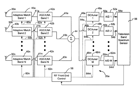
FIG. la is a schematic diagram of one embodiment of a radio frequency front
end 20a in accordance with the invention for a television band receiver
provisioned with a television band receiver and spectrum sensor 56 for
identifying television band white spaces. In accordance with the invention,
the
radio frequency (RF) front end 20a is connected to a plurality of antennas 30a-
30n. As understood by those skilled in the art, the number of antennas 30a-30n
CA 02810231 2013-03-22
Our Ref: 1029P015CA01 - 6 -
is dependent on the range of spectrum to be searched for white spaces, which
may all or any part of the range from 50-700 MHz. As also understood by those
skilled in the art, the type and configuration of each antenna 30a-30n is
based
both on the spectrum of interest as well as design choice, as will be
explained
below in more detail with reference to FIG. 7.
Each antenna 30a-30n is connected to a respective adaptive matching network
40a-40n of the RF front end 20. Each adaptive matching network 40a-40n can
be selectively and dynamically tuned to a desired frequency within a receiver
range of the corresponding antenna 30a-30n by a RF front end control 58 using
signal lines 60a-60n, as will be explained below in more detail with reference
to
FIG. 8. The RF front end control 58 responds to instructions received from a
television band spectrum sensor 56, which may be implemented in any one of
many ways known in the art. The television band spectrum sensor 56 is not
within the scope of this invention.
Output from each adaptive matching network 40a-40n is passed via a
respective connection 41a-41n to an automatic gain controller (AGC) and a low
noise amplifier (LNA) circuit 42a-42n. As will be further explained below with
reference to FIG. 7, the purpose of the AGC/LNA circuits 42a-42n is to balance
signals received by the respective antennas 30a-30n so that weak signals (e.g.
wireless microphone and other narrowband signals) are not drowned out by
strong signals (e.g. DTV broadcasts originating in close proximity to the RF
front
end 20). The automatic gain controller is regulated by an automatic gain
control
threshold voltage that is supplied to the AGC/LNA circuits 42a-42n by the RF
front end control 58 via respective control circuits 62a-62n, as will also be
explained in more detail below with reference to FIG. 7. Output of each
AGC/LNA circuit 42a-42n is passed via respective connections 43a-43n to a
signal summer (combiner) 44, which may be may be implemented, for example,
as a resistor network that is known in the art. The combined signal is output
via
respective connections 46a-46m to a plurality of downconverter/tuners
(DC/tuners) 48a-48m. The number of DC/tuners 48a-48m is independent of the
number of adaptive matching networks 40a-40n, and there is no requirement for
a 1 to 1 correspondence between the two. In one embodiment of the invention,
CA 02810231 2013-03-22
Our Ref: 1029P015CA01 - 7 -
the DC/tuners 48a-48m are DTV tuner integrated circuits (ICs) available from
Infineon Technologies AG under part number TUA-8045.
Each DC/tuner 48a-48m is controlled by the RF front end control 58 via
connections 64a-64m to select (tune to) a particular RF frequency generally
having a bandwidth of about 6-8 MHz. The RF frequency to be selected by each
DC/tuner 48a-48m is dictated by the television band spectrum sensor 56, and
communicated to the DC/tuner 48a-48m by the RF front end control 58 via
signal connections 62a-62n. The DC/tuner 48a-48m down converts the RF
frequency to an intermediate frequency (IF) suitable for digitization, in a
manner
well known in the art. The IF output by the DC/tuner 46a-46m is conducted via
a
respective connection 50a-50m to an analog-to-digital (AID) converter 52a-52m.
The IF is sampled by the respective ND converters 52a-52m at a
predetermined sampling rate (generally 2-4 times the ATSC symbol rate) to
produce a digital representation of the IF signal, which is output via
respective
connections 54a-54m to the television band spectrum sensor 56.
FIG. lb is a schematic diagram of another embodiment of a radio frequency
front end 20b in accordance with the invention. In this embodiment, the number
of downconverter/tuners 46a-n is equal to the number of adaptive matching
networks 40a-n. Consequently, the signal summer 44 described above with
reference to FIG. 1 a is not required and there is a direct connection between
each AGC/LNA circuit 42a-42n and the corresponding downconverter/tuner
48a-48n. Otherwise, the radio frequency from end 20b is identical to that
described above with reference to FIG. 1 a. It should be understood that
Although this configuration is not repeated for each of the embodiments
described below with reference to FIGs. 2-6, any one of those embodiments can
be constructed as shown in FIG. lb so long as the number of
downconverter/tuners is equal to the number of adaptive matching networks,
and hence the number of antennas connected to the RF front end.
FIG. 2 is a schematic diagram of another embodiment of a radio frequency front
end 22 in accordance with the invention. The RF front end 22 is identical to
the
embodiment described above with reference to FIG. la with an exception that
CA 02810231 2013-03-22
Our Ref: 1029P015CA01 - 8 -
the outputs of the DC/tuner 48a-48m are routed via respective connections 49a-
49m to an IF summer (IF combiner) 51, which may be implemented in the same
way as the signal summer 44 described above with reference to FIG. 1a. The
combined IF signal is passed via a connection 53 to an AID converter 52, which
samples the combined IF signal at the predetermined sampling rate and outputs
a digital representation of the combined IF signal via connection 54 to the
television band spectrum sensor 56.
FIG. 3 is a schematic diagram of yet another embodiment of a radio frequency
front end 24 in accordance with the invention. The RF front end 24 is
identical to
the embodiment described above with reference to FIG. 1a, with an exception
that the output from each of the antennas 30a-30n may be shunted to ground
(disabled) by a respective switch 70a-70n for any one or more of a number of
reasons determined by the television band spectrum sensor 56. The switches
70a-70n are controlled by the RF front end control 58, under direction of the
television band spectrum sensor 56, using respective connections 72a-72n to
apply a control voltage in a manner known in the art.
FIG. 4 is a schematic diagram of yet a further embodiment of a radio frequency
front end 26 in accordance with the invention. The RF front end 26 is
identical to
the embodiment described above with reference to FIG. 3, with an exception
that output of the DC/tuner 48a-48m is routed to the IF signal summer 51 and
digitized by the ND converter 52, as described above with reference to FIG. 2.
FIG. 5 is a schematic diagram of still a further embodiment of a radio
frequency
front end 28 in accordance with the invention. The RF front end 28 is
identical to
the embodiment described above with reference to FIG. 4, with an exception
that operation of the respective DC/tuner 48a-48m is further enhanced by the
addition of IF filters and IF filter selectors 78a-78m. Each group of IF
filters and
the associated IF filter selector 78a-78m receives an IF signal output by the
associated DC/tuner 48a-48m and passes the IF signal through a selected IF
filter, as will be explained below in more detail with reference to FIG. 7.
The
filtered IF signal is routed back to the DC/tuner 48a-48m, which may further
down convert the IF signal before it is passed to the associated AID converter
CA 02810231 2013-03-22
Our Ref: 1029P015CA01 - 9 -
52a-52m as described above with reference to FIG. la. The selection of the
appropriate IF filter by an IF filter selector is controlled by the RF front
end
control 58, under the direction of the television band spectrum sensor 56,
using
signal connections 80a-80m.
FIG. 6 is a schematic diagram of yet one more embodiment of a radio frequency
front end 32 in accordance with the invention. The RF front end 32 is
identical to
the embodiment described above with reference to FIG. 5, with an exception
that output of the DC/tuner 48a-48m is routed to the IF signal summer 51 and
digitized by the AID converter 52, as described above with reference to FIG.
2.
FIG. 7 is a schematic diagram of one implementation of the radio frequency
front end 28 shown in FIG. 5. In this implementation, the RF front end 28 is
connected to three antennas 100a. 100b and 100c. The antennas 100a and
100b are disc-cone antennas, well known in the art. Antenna 100a can be
dynamically tuned, for example, to receive signals in the 50 MHz-150 MHz
range. Antenna 100b can be dynamically tuned, for example, to receive signals
in the 150 MHz-350 MHz range. Antenna 100c is, for example, a simple loop
antenna which can be dynamically tuned to receive signals in the 350 MHz-700
MHz range. The respective antennas 100a-100c are connected to a respective
balun 102a-102c, which converts the balanced antenna output to an
unbalanced signal, in a manner well known in the art. Each balun 102a-102c is
coupled via a connector 104a-104c to a respective adaptive matching network
40a-40c of the RF front end 28. The adaptive matching networks 40a-40c
respectively include a tunable matching network 106a-106c and a pin diode
attenuator 114a-114c, an exemplary structure and function of adaptive matching
networks 40a-40c will be described below with reference to FIG. 8.
Each tunable matching network 106a-106c is dynamically tuned, as will be
explained below with reference to FIG. 8, by a control voltage applied via
control
lines 112a-112c by a digital potentiometer 110, the construction and function
of
which is know in the art. The digital potentiometer 110 is coupled via a
charge
isolator 108 to a data line (SDA) and a data clock line (SCL) coupled to the
RF
front end control 58. The RF front end control 58 provides data to the digital
CA 02810231 2013-03-22
Our Ref: 1029P015CA01 - 10 -
potentiometer 110 to regulate the respective control voltages supplied to the
tunable matching networks 106a-106b. Output from the adaptive matching
networks 40a-40c flows to a respective low noise amplifier (LNA) 116a-116c,
which provides a 20-30 bB gain to the output signal. Output of the respective
LNAs 116a-116c is fed back through a respective diode 118a-118c to an
automatic gain controller (AGC) 120a-120c, which compares the feedback to an
AGC threshold voltage applied via control lines 126a-126c by a digital
potentiometer 124. The digital potentiometer 124 is coupled to the RE front
end
control 58 through a charge isolator 122 to the data line (SDA) and the data
clock line (SCL). The RF front end control 58 provides data to the digital
potentiometer 124 to control each of the AGC threshold voltages 126a-126c.
The charge isolators 108, 122 isolate the control circuits from the receiver
circuits to minimize electronic noise transfer. The charge isolators 108, 124
may
be optical isolators, for example, which are known in the art. The AGC 120a-
120c applies a control voltage to the pin diode attenuator 114a dependent on a
power difference between the signal fed back through diode 118a-118c and the
respective AGC threshold voltage applied via control lines 126a-126c, so that
strong signals are attenuated by the pin diode attenuator 114a-114c.
Output from the LNAs 116a-116b is combined by a signal summer circuit 44,
examples of which are well known in the art. The combined signal is fed in
parallel via connections 128a and 128b to respective DC/tuners (for example,
DTV tuner ICs) 130a-130b. As described above, the DC/tuners 130a and 130b
are, for example, the lnfineon Technologies TUA-6045 DTV tuner ICs. The
combined signal is down sampled by the respective DC/tuners 130a, 130b in a
manner known in the art to provide an intermediate frequency (IF) signal that
is
output via respective connections 131a and 131b to respective switch pairs
132a-134a and 132b-134b. The switch pairs 132a-134a and 132b-134b are
respectively controlled in unison by the RE front end control 58 via signal
lines
136a (Tuner Filter 1) and 136b (Tuner Filter 2) to select an IF filter, or to
bypass
the IF filters. In this example, the switch pairs 132a-134a and 132b-134b are
three pole switches that are used to select one of two IF filters 138 or 140
and
142 or 144, respectively. The IF filters may be bypassed by moving the switch
CA 02810231 2013-03-22
Our Ref: 1029P015CA01 -11 -
pairs 132a and 134a or 132b and 134b to a center position to select a
respective filter bypass line 135a and 135b. The IF filters 138-144 are
statically
implemented to filter out all but a selected piece of the combined signal in
order
to reduce noise in the respective DC/tuners 130a and 130b. The respective
filters are selected by the RF front end control 58 based on a piece of
spectrum
of interest. Although in this exemplary embodiment 2 IF filters are associated
with each of the DC/tuners 130a and 130b, it should be understood that the
invention is not limited to this exemplary implementation. Output from the
respective switches 134a and 134b is fed back to the respective DC/tuners
130a and 130b via connections 137a and 137b.
A tuning function of each of the DC/tuners 130a and 130b is controlled by the
RF front end control 58 via a respective data line (SDA) and a data clock line
(SCL) to tune the respective DC/tuners to a particular piece of the IF signal
returned via connections 137a and 137b. Timing signals output by a crystal
oscillator (XTAL) 152 are used by the respective DC/tuners 130a, 130b for
tuning functions in a manner well known in the art. Output from the respective
DC/tuners 130a and 130b is passed through a respective balun 154a and 154b
to a respective analog-to-digital (AID) converter 156a and 156b which converts
the respective analog signals output by the DC/tuners 130a and 130b to a
digital representation of the output, in a manner well known in the art. The
digital
signals are output to the television band spectrum sensor 56, which processes
the digital signals in accordance with a known white space sensor algorithm to
detect television band white spaces.
FIG. 8 is a schematic diagram of one implementation of the adaptive matching
network 40a of the radio frequency front end shown in FIG. 7. The antenna
100a is connected at 300 to the adaptive matching network 40a. A bypass
connector 302 permits the adaptive matching network 40a to be bypassed. A
single pole double throw switch (SPDTS) 305 controlled by the RF front end
control 58 via tuner bypass 350 is used to select output from the adaptive
matching network 40a or the bypass connector 302, as will be explained below
in more detail.
CA 02810231 2013-03-22
Our Ref: 1029P015CA01 - 12 -
In this embodiment, the adaptive matching network 40a includes an impedance
transformer and low pass filter 304, the pin diode attenuator 114a, a shunt
resonant block 326 and a series resonant block 338. The shunt resonant block
326 and the series resonant block 338 collectively form the tunable matching
network 106a shown in FIG 5. The impedance transformer and low pass filter
304 translates the impedance of the antenna 100a to a different impedance for
maximum signal power transfer. The impedance transformer and low pass filter
304 includes a series connected capacitor 306 and inductor 308, and a
branched capacitor 310 connected to ground, a value of each of which is
selected in a manner known in the art to perform the desired impedance
translation. The pin diode attenuator 114a is controlled by a control voltage
output by the AGC 120a to a control line 121a. The control voltage is applied
to
interconnected resistor 314a, 314b and capacitor/ground 316a, 316b circuits
that are respectively connected to diodes 318a and 318b which prevent current
flow to the AGC 120a. The control voltage is applied to opposite terminals of
a
capacitor 320, a resistor 322, and an inductor 324 to attenuate or boost a
received signal, as desired. Output of the pin diode attenuator 114a flows to
the
shunt resonant block 326 which prevents the received signal from shunting to
ground.
The shunt resonant block 326 includes a capacitor 328 having its output
terminal connected to parallel connected inductor 330 and varactor 332.
Capacitance of the varactor 332 is controlled by control voltage applied by
the
RF front end control 58 to a Tuner Band conductor 336 connected to a resistor
334. The series resonant block 338 boosts the received signal. The series
resonant block 338 includes a varactor 340 connected in series with an
inductor
344. The Tuner Band 336 control voltage is applied through resistor 342 to
control a capacitance of the varactor 340. The Tuner Band 336 control voltage
is selected by the RF front end control 58 using, for example, a lookup table
(not
shown) to dynamically tune the antenna 100a to a desired piece of the
television band spectrum. The component values for the components of the
shunt resonant block 326 and the series resonant block 338 are selected, for
example, using a Smith Chart in a manner known in the art.
CA 02810231 2013-03-22
Our Ref: 1029P015CA01 - 13 -
As explained above, selection of the adaptive matching network 40a or the
bypass 302 is controlled by the RF front end control 58, which applies a
control
voltage to a Tuner Bypass 350 connected to series connected inverters 352a
and 352b. The inverter 352a is coupled to a capacitor 354. When the Tuner
Bypass 350 is driven low, the inverter 352a drives lines 356 and 358 high and
the inverter 352b drives line 360 low, which causes the SPDTS 304 to switch
output of the adaptive matching network 40a to RF_Out 362. When Tuner
Bypass 350 is driven high, the inverter 352a drives lines 356 and 358 low and
inverter 352b drives line 360 high, which causes the SPDTS 304 to switch
output of the bypass 302 to RF_Out 362. Thus, the RE front end control 58 is
afforded complete control of the adaptive matching network 40a.
FIG. 9 is a schematic diagram of another embodiment of the radio frequency
front end 28 in accordance with the invention. This embodiment is the similar
to
the embodiment described above with reference to FIGs. 1a and 2-5, except
that the AGC/LNA circuits 42a-42n are replaced by LNA/AGC circuits 45a-45n.
It has been determined that signal detection performance can be yet further
improved, especially in very noisy environments, if the received signal is
amplified by the low noise amplifier (LNA) prior to received signal treatment
by
the AGC (pin diode attenuator). This configuration of the radio frequency
front
end 28 will be explained below in more detail with reference to FIGs. 11-14.
All
other components of the radio frequency front end 28 are the same as those
described above with reference to FIGs. la and 2-5 and that description will
not
be repeated.
FIG. 10 is a schematic diagram of the embodiment of the radio frequency front
end shown in FIG. 9 with cyclostationary feature detection. The detection of a
very low power signal about which no structure is known is the basis of an
area
of study called Low Probability of Detection/Low Probability of Interference
(LPD/LPI) communications. In situations where energy detectors, such as the
radio frequency front end 28, detection may be enhanced using cyclostationary
feature detection. It has been determined that a radio frequency front end 28
with cyclostationary feature detection shown in FIG. 10 may detect the
presence
of a signal 30 dB below its in-band noise floor.
CA 02810231 2013-03-22
Our Ref: 1029P015CA01 - 14 -
The radio frequency front end 28 with cyclostationary feature detection
exploits
the fact that in a manmade signal some periodic repetition is always present.
This periodicity may be the bit rate used, the chip rate used (in direct
sequence
spread spectrum), or the frame rate used. While there is no spectral "tone" in
the actual signal, a spectral "tone" is created through a non-linear operation
on
the received signal.
One implementation of this non-linear operation is a delay and multiply
operation shown in FIG. 10. The output of the AID converters 52a-52m is
delayed by a delay circuit 57a-57m by approximately one half of a period of
the
underlying bit rate, chip rate, or frame rate. The delayed signal is then
multiplied
with a current sample of the ND output by a multiplier circuit 59a-59m. The
actual delay time created by the delay circuits 57a-57m is not critical. One
half
of the underlying period maximizes the "tone" to self-interference (noise)
ratio,
but the ratio tends to be insensitive to actual delay time. The "tone" appears
at
a frequency corresponding to the bit rate, the chip rate, or the frame rate.
The radio frequency front end 28 with cyclostationary feature detection
requires
a dynamic range that can "reach" down into the noise to detect a weak signal.
Consequently, the A/D converters 52a-52m must have a reasonably large
dynamic range.
In this embodiment, the cyclostationary feature detection can be bypassed
under control of the RF front end control 58, which applies appropriate
control
voltages to control lines 61a-61m to control bi-pole switches 55a-55m to shunt
the output of the ND converters 52a-52m directly to the television band
spectrum sensor 56 via respective signal lines 54a-54m when the
cyclostationary feature detection is to be bypassed.
FIG. 11 is a schematic diagram of one implementation of the radio frequency
front end 28 shown in FIGs. 9 and 10. In this implementation, a radio
frequency
front end 928a includes respective LNA/AGC/matching networks 240a-240c.
The LNA/AGC/matching networks 240a-240c include low noise amplifiers
(LNAs) 116a-116c. The (LNAs) 116a-116c provide a 20-30 bB gain to the radio
frequency signal outputs of respective antennas 100a-100c, which they receive
CA 02810231 2013-03-22
Our Ref: 1029P015CA01 - 15 -
via optional baluns 102a-102c. Pin diode attenuator circuits 114a-114c are
respectively connected to the output ends of the LNAs 116a-116c. Attenuation
control lines (RF AGC 1-3) 126a-126c are respectively connected to the
respective pin diode attenuator circuits 114a-114c. In this embodiment the
control lines 126a-126c are respectively connected to an RF AGC selector 115,
used to switch the output of control voltages received from RF AGC circuits
embedded in the respective tuner ICs 130a, 130b. Control of the RF AGC
selector 115 may be manual, i.e. preset using dipole switches, for example, or
they may be dynamically controlled by the RF front end control 58 in a manner
well known in the art. The attenuated RF output of the respective pin diode
attenuators 114a-114c is passed to respective tunable matching networks 106a-
106c as will explained below in more detail with reference to FIGs. 17 and 18.
Each tunable matching network 106a-106c is respectively connected to the
input end of a buffer amplifier 117a-117c. The buffer amplifiers 117a-117c
respectively buffer the input signals to a higher level for the tuner circuits
130a,
130b, which have a higher noise floor than the RF antenna signals. In all
other
respects this implementation is the same as the one described above with
respect to FIG. 7 and it will not be further described.
FIG. 12 is a schematic diagram of another implementation of the radio
frequency front end 28 shown in FIGs. 9 and 10. In this implementation a
digital
signal processor (DSP) 123 of RF front end 928b sets directly the RF AGC
126a-126c without using signal feedback. The DSP 123 is provided samples of
a number of on board voltages. For example, the pin diode attenuator control
voltages 126a-126c: intermediate frequency (IF) AGC control voltages, and
reference voltages. The DSP 123 uses these voltages to compute an
appropriate AGC control. In one embodiment, the DSP 123 maps the monitored
voltages into a lookup table to determine an attenuation (in dB) for the pin
diode
attenuators 114a-114c, which is translated into an appropriate RF AGC control
voltage. In all other respects this embodiment is the same as the embodiment
shown in FIG. 11.
FIG. 13 is a schematic diagram of a further implementation of the radio
frequency front end shown in FIGs. 9 and 10. In this implementation a RF front
CA 02810231 2013-03-22
Our Ref: 1029P015CA01 - 16 -
end 928c runs an ND monitor process 127 that monitors various analog inputs,
for example the analog inputs described above with reference to FIG. 12. The
AID monitor process 127 then computes an RF AGC which it outputs via line
129 to the RF front end control 58. The RF front end control 58 translates the
RF AGC to a control voltage applied to respective control voltage lines 126a-
126c to control the respective pin diode attenuators 114a-114c. In all other
respects this embodiment is the same as the embodiment shown in FIG. 11.
FIG. 14 is a schematic diagram of yet a further implementation of the radio
frequency front 28 end shown in FIGs. 9 and 10. In this implementation an RF
front end 928d generates RF AGC control voltages using the buffer amplifiers
117a-117c to directly control attenuation by the pin diode attenuator circuits
114a-114c. Diodes 119a-119c respectively prevent feedback to the buffer
amplifiers 117a-117c. In all other respects this embodiment is the same as the
embodiment shown in FIG. 11.
FIG. 15 is a schematic diagram of an example of a single band implementation
of the radio frequency front end 28 shown in FIG. 9. In this implementation a
RF
front end 928e has only one antenna 100 that is adapted to receive RF signals
around a frequency of interest. The antenna 100.may be any known type of
antenna that is suitable for the desired frequency band. The pin diode
attenuator 114 may also be set to a predetermined attenuation level by
applying
a fixed RF AGC control voltage in a manner well known in the art. The tunable
matching network 106 is controlled by the RF front end control 58 to tune the
antenna 100 to the frequency of interest. The buffer amplifier 117 applies a
predetermined boost to the received RF signal as described above with
reference to FIG. 11. The other components of the RF front end 928e are as
described above and will not be further described.
FIG. 16 is a schematic diagram of another example of a single band
implementation of the radio frequency front end 28 shown in FIG. 9. In this
implementation an RF front end 928f is the same as the one described above
with reference to FIG. 14, except that the tunable matching network is omitted
to
CA 02810231 2013-03-22
Our Ref: 1029P015CA01 - 17 -
reduce cost. The other components of the RF front end 928f are as described
above and will not be further described.
FIG. 17 is a schematic diagram of one implementation of a received signal
amplification/attenuation stage and an adaptive matching network of the radio
frequency front end shown in FIGs. 11-15. The antenna 100a is connected at
300 to an optional impedance transformer and low pass filter 304, which is in
turn connected to the LNA 316 that amplifies the RF signal received by the
antenna 100 as described above. The optional impedance transformer and low
pass filter 304 translates the impedance of the antenna 100a to a different
impedance for maximum signal power transfer. The impedance transformer and
low pass filter 304 includes a series connected capacitor 306 and inductor
308,
and a branched capacitor 310 connected to ground, a value of each of which is
selected in a manner known in the art to perform the desired impedance
translation.
The output pin of the LNA 316 is connected to the pin diode attenuator 114.
The
pin diode attenuator 114 is controlled by the RF AGC control voltage output to
a
control line 121. The control voltage is applied to interconnected resistors
314a,
314b and capacitor/ground circuits 316a, 316b that are respectively connected
to diodes 318a and 318b which prevent current flow to the RF AGC control line.
The control voltage is applied to opposite terminals of a capacitor 320, a
resistor
322, and an inductor 324 to attenuate or boost a received signal, as desired.
Output of the pin diode attenuator 114 flows to a shunt resonant block 326
which prevents the received signal from shunting to ground.
The shunt resonant block 326 and a series resonant block 338 collectively form
the tunable matching networks 106 shown in FIGs. 11-16. The shunt resonant
block 326 includes a capacitor 328 having its output terminal connected to
parallel connected inductor 330 and varactor 332. Capacitance of the varactor
332 is controlled by control voltage applied by the RF front end control 58 to
a
Tuner Band conductor 336 connected to a resistor 334. The series resonant
block 338 boosts the received signal. The series resonant block 338 includes a
varactor 340 connected in series with an inductor 344. The Tuner Band 336
CA 02810231 2013-03-22
Our Ref: 1029P015CA01 - 18 -
control voltage is applied through resistor 342 to control a capacitance of
the
varactor 340. The Tuner Band 336 control voltage is selected by the RF front
end control 58 using, for example, a lookup table (not shown) to dynamically
tune the antenna 100a to a desired piece of the television band spectrum. The
component values for the components of the shunt resonant block 326 and the
series resonant block 338 are selected, for example, using a Smith Chart in a
manner known in the art.
A bypass connector 302 permits the adaptive matching network 40a to be
bypassed. A single pole double throw switch (SPDTS) 305 controlled by the RF
front end control 58 via tuner bypass 350 is used to select output from the
adaptive matching network 40a or the bypass connector 302, as will be
explained below in more detail.
As explained above, selection of the tunable matching network or the bypass
302 is controlled by the RF front end control 58, which applies a control
voltage
to a Tuner Bypass 350 connected to series connected inverters 352a and 352h.
The inverter 352a is coupled to a capacitor 354. When the Tuner Bypass 350 is
driven low, the inverter 352a drives lines 356 and 358 high and the inverter
352b drives line 360 low, which causes the SPDTS 304 to switch output of the
adaptive matching network 40a to RF_Out 362. When Tuner Bypass 350 is
driven high, the inverter 352a drives lines 356 and 358 low and inverter 352b
drives line 360 high, which causes the SPDTS 304 to switch output of the
bypass 302 to RF_Out 362. Thus, the RF front end control 58 is afforded
complete control of the tunable matching network 106.
FIG. 18 is a schematic diagram of an implementation of a received signal
amplification/attenuation stage 242 for the radio frequency front end 928f
shown
in FIG. 16. This implementation does not include the tunable matching network
106 or the tuner bypass control circuit. Otherwise, it is the same as the
implementation described above with reference to FIG. 17.
The embodiments of the invention described above are intended to be
exemplary only of the radio frequency front end for a television band receiver
and spectrum sensor in accordance with the invention. The scope of the
CA 02810231 2013-03-22
Our Ref: 1029P015CA01 - 19 -
invention is therefore intended to be limited only by the scope of the
appended
claims.