Note: Descriptions are shown in the official language in which they were submitted.
CA 02810394 2013-03-04
WO 2012/031178 PCT/US2011/050292
1
A LIGHT EMITTING APPARATUS
FIELD OF THE INVENTION
The present invention in general is related to light emitting and photovoltaic
technology and, in particular, is related to a light emitting apparatus having
light emitting or
photovoltaic diodes and methods of making the same.
BACKGROUND OF THE INVENTION
Lighting devices having light emitting diodes ("LEDs") have typically required
creating the LEDs on a semiconductor wafer using integrated circuit process
steps. The resulting
LEDs are substantially planar and comparatively large, on the order of two
hundred or more
microns across. Each such LED is a two terminal device, typically having two
metallic terminals
on the same side of the LED, to provide Ohmic contacts for p-type and n-type
portions of the
LED. The LED wafer is then divided into individual LEDs, typically through a
mechanical
process such as sawing. The individual LEDs are then placed in a reflective
casing, and bonding
wires are individually attached to each of the two metallic terminals of the
LED. This process is
time consuming, labor intensive and expensive, resulting in LED-based lighting
devices which
are generally too expensive for many consumer applications.
Similarly, energy generating devices such as photovoltaic panels have also
typically required creating the photovoltaic diodes on a semiconductor wafer
or other substrates
using integrated circuit process steps. The resulting wafers or other
substrates are then packaged
and assembled to create the photovoltaic panels. This process is also time
consuming, labor
intensive and expensive, resulting in photovoltaic devices which are also too
expensive for
widespread use without being subsidized by third parties or without other
governmental
incentives.
Various technologies have been brought to bear in an attempt to create new
types
of diodes or other semiconductor devices for light emission or energy
generation purposes. For
example, it has been proposed that quantum dots, which are functionalized or
capped with
organic molecules to be miscible in an organic resin and solvent, may be
printed to form graphics
which then emit light when the graphics are pumped with a second light.
Various approaches for
device formation have also been undertaken using semiconductor nanoparticles,
such as particles
in the range of about 1.0 nm to about 100 nm (one-tenth of a micron). Another
approach has
utilized larger scale silicon powder, dispersed in a solvent-binder carrier,
with the resulting
CA 02810394 2013-03-04
WO 2012/031178 PCT/US2011/050292
2
colloidal suspension of silicon powder utilized to form an active layer in a
printed transistor. Yet
another different approach has used very flat AlInGaP LED structures, formed
on a GaAs wafer,
with each LED having a breakaway photoresist anchor to each of two neighboring
LEDs on the
wafer, and with each LED then picked and placed to form a resulting device.
None of these approaches have utilized an ink or suspension containing
semiconductor devices, which are completed and capable of functioning, which
can be formed
into an apparatus or system in a non-inert, atmospheric air environment, using
a printing process.
These recent developments for diode-based technologies remain too complex and
expensive for LED-based devices and photovoltaic devices to achieve commercial
viability. As a
consequence, a need remains for light emitting and/or photovoltaic apparatuses
which are
designed to be less expensive, in terms of incorporated components and in
terms of ease of
manufacture. A need also remains for methods to manufacture such light
emitting or
photovoltaic devices using less expensive and more robust processes, to
thereby produce LED-
based lighting devices and photovoltaic panels which may be available for
widespread use and
adoption by consumers and businesses. Various needs remain, therefore, for a
liquid suspension
of completed, functioning diodes which is capable of being printed to create
LED-based devices
and photovoltaic devices, for a method of printing to create such LED-based
devices and
photovoltaic devices, and for the resulting printed LED-based devices and
photovoltaic devices.
SUMMARY
The exemplary embodiments provide a "diode ink", namely, a liquid suspension
of diodes which is capable of being printed, such as through screen printing
or flexographic
printing, for example. As described in greater detail below, the diodes
themselves, prior to
inclusion in the diode ink composition, are fully formed semiconductor devices
which are
capable of functioning when energized to emit light (when embodied as LEDs) or
provide power
when exposed to a light source (when embodied as photovoltaic diodes). An
exemplary method
also comprises a method of manufacturing diode ink which, as discussed in
greater detail below,
suspends a plurality of diodes in a solvent and viscous resin or polymer
mixture which is capable
of being printed to manufacture LED-based devices and photovoltaic devices.
Exemplary
apparatuses and systems formed by printing such a diode ink are also
disclosed. While the
description is focused on diodes, those having skill in the art will recognize
that other types of
semiconductor devices may be substituted equivalently to form what is referred
to more broadly
CA 02810394 2013-03-04
WO 2012/031178 PCT/US2011/050292
3
as a "semiconductor device ink", and that all such variations are considered
equivalent and
within the scope of the disclosure.
An exemplary embodiment is a composition comprising: a plurality of diodes; a
first solvent; and a viscosity modifier. In an exemplary embodiment, the first
solvent may
comprise at least one solvent selected from the group consisting of: water;
alcohols such as
methanol, ethanol, N-propanol (including 1-propanol, 2-propanol (IPA)),
butanol (including 1-
butanol, 2- butanol (isobutanol)), pentanol (including 1- pentanol, 2-
pentanol, 3- pentanol),
octanol, tetrahydrofurfuryl alcohol (THFA), cyclohexanol, terpineol; ethers
such as methyl ethyl
ether, diethyl ether, ethyl propyl ether, and polyethers; esters such ethyl
acetate; glycols such as
ethylene glycols, diethylene glycol, polyethylene glycols, propylene glycols,
glycol ethers, glycol
ether acetates; carbonates such as propylene carbonate; glycerin,
acetonitrile, tetrahydrofuran
(THF), dimethyl formamide (DMF), N-methyl formamide (NMF), dimethyl sulfoxide
(DMS0);
and mixtures thereof.
In an exemplary embodiment, the first solvent comprises N-propanol. The first
solvent may be present in an amount of about 5 percent to 50 percent by
weight. In an exemplary
embodiment, the viscosity modifier comprises a methoxyl cellulose resin or a
hydroxypropyl
cellulose resin. The viscosity modifier may be present in an amount of about
0.75% to 5% by
weight.
The viscosity modifier, in an exemplary embodiment, comprises at least one
viscosity modifier selected from the group consisting of: clays such as
hectorite clays, garamite
clays, organo-modified clays; saccharides and polysaccharides such as guar
gum, xanthan gum;
celluloses and modified celluloses such as hydroxyl methyl cellulose, methyl
cellulose, methoxyl
cellulose, carboxymethyl cellulose, hydroxyethyl cellulose and hydroxypropyl
cellulose,
cellulose ether, cellulose ethyl ether, chitosan; polymers such as acrylate
and (meth)acrylate
polymers and copolymers, diethylene glycol, propylene glycol, fumed silica,
silica powders;
modified ureas; and mixtures thereof.
In an exemplary embodiment, the composition further comprises a second solvent
different from the first solvent. The second solvent may be at least one
solvent selected from the
group consisting of: water; alcohols such as methanol, ethanol, N-propanol
(including 1-
propanol, 2-propanol (isopropanol)), isobutanol, butanol (including 1-
butanol, 2- butanol),
pentanol (including 1- pentanol, 2- pentanol, 3- pentanol), octanol,
tetrahydrofurfuryl alcohol,
cyclohexanol; ethers such as methyl ethyl ether, diethyl ether, ethyl propyl
ether, and polyethers;
esters such ethyl acetate, dimethyl adipate, proplyene glycol monomethyl ether
acetate, dimethyl
CA 02810394 2013-03-04
WO 2012/031178 PCT/US2011/050292
4
glutarate, dimethyl succinate; glycols such as ethylene glycols, diethylene
glycol, polyethylene
glycols, propylene glycols, glycol ethers, glycol ether acetates; carbonates
such as propylene
carbonate; glycerin, acetonitrile, tetrahydrofuran (THF), dimethyl formamide
(DMF), N-methyl
formamide (NMF), dimethyl sulfoxide (DMS0); and mixtures thereof.
The second solvent may be at least one dibasic ester. The second solvent may
comprise a solvating agent or a wetting solvent. In an exemplary embodiment,
the second
solvent comprises: dimethyl glutarate and dimethyl succinate; wherein the
ratio of dimethyl
glutarate to dimethyl succinate is about two to one (2:1). In another
exemplary embodiment, the
second solvent may be present in an amount of about 0.1% to 10% by weight. In
another
exemplary embodiment, the second solvent may be present in an amount of about
0.5% to 6% by
weight.
In an exemplary embodiment, the first solvent comprises N-propanol, terpineol
or
diethylene glycol, ethanol, tetrahydrofurfuryl alcohol, cyclohexanol or
mixtures thereof, and
present in an amount of about 5% to 50% by weight; the viscosity modifier
comprises methoxyl
cellulose or hydroxypropyl cellulose resin, and present in an amount of about
0.75% to 5.0% by
weight; the second solvent comprises a nonpolar resin solvent present in an
amount of about
0.5% to 10% by weight; and wherein the balance of the composition further
comprises water.
A method of making the composition is also disclosed, and an exemplary method
embodiment comprises: mixing the plurality of diodes with N-propanol; adding
the mixture of
the N-propanol and plurality of diodes to the methyl cellulose resin; adding
the dimethyl
glutarate and dimethyl succinate; and mixing the plurality of diodes, N-
propanol, methyl
cellulose resin, dimethyl glutarate and dimethyl succinate for about 25 to 30
minutes in an air
atmosphere.
The exemplary method may further comprise releasing the plurality of diodes
from a wafer. In an exemplary embodiment, the step of releasing the plurality
of diodes from the
wafer further may further comprise grinding and polishing a back side of the
wafer. In another
exemplary embodiment, the step of releasing the plurality of diodes from the
wafer further may
further comprise a laser lift-off from a back side of the wafer.
In another exemplary embodiment, the first solvent comprises about 15% to 40%
by weight of N-propanol, terpineol or diethylene glycol, ethanol,
tetrahydrofurfuryl alcohol, or
cyclohexanol; the viscosity modifier comprises about 1.25% to 2.5% by weight
of methoxyl
cellulose or hydroxypropyl cellulose resin; the second solvent comprises about
0.5% to 10% by
weight of a nonpolar resin solvent; and the balance of the composition further
comprises water.
CA 02810394 2013-03-04
WO 2012/031178 PCT/US2011/050292
5
In another exemplary embodiment, the first solvent comprises about 17.5% to
22.5% by weight of N-propanol, terpineol or diethylene glycol, ethanol,
tetrahydrofurfuryl
alcohol, or cyclohexanol; the viscosity modifier comprises about 1.5% to 2.25%
by weight of
methoxyl cellulose or hydroxypropyl cellulose resin; the second solvent
comprises about 0.01%
to 6.0% by weight of at least one dibasic ester; the balance of the
composition further comprises
water; and the viscosity of the composition is substantially between about
5,000 cps to about
20,000 cps at 25 C.
In yet another exemplary embodiment, the first solvent comprises about 20% to
40% by weight of N-propanol, terpineol or diethylene glycol, ethanol,
tetrahydrofurfuryl alcohol,
and/or cyclohexanol; the viscosity modifier comprises about 1.25% to 1.75% by
weight of
methoxyl cellulose or hydroxypropyl cellulose resin; the second solvent
comprises about 0.01%
to 6.0% by weight of at least one dibasic ester; the balance of the
composition further comprises
water; and wherein the viscosity of the composition is substantially between
about 1,000 cps to
about 5,000 cps at 25 C.
In various exemplary embodiments, the composition may have a viscosity
substantially between about 1,000 cps and about 20,000 cps at about 25 C, or
may have a
viscosity of about 10,000 cps at about 25 C.
In an exemplary embodiment, each diode of the plurality of diodes comprises
GaN and a silicon substrate. In another exemplary embodiment, each diode of
the plurality of
diodes comprises a GaN heterostructure and GaN substrate. In various exemplary
embodiments,
the GaN portion of each diode of the plurality of diodes is substantially
lobed, stellate, or
toroidal.
In various exemplary embodiments, each diode of the plurality of diodes has a
first metal terminal on a first side of the diode and a second metal terminal
on a second, back side
of the diode. In other exemplary embodiments, each diode of the plurality of
diodes has only one
metal terminal or electrode.
In another exemplary embodiment, each diode of the plurality of diodes has at
least one metal via structure extending between at least one p+ or n+ GaN
layer on a first side of
the diode to a second, back side of the diode. In various exemplary
embodiments, the metal via
structure comprises a central via, a peripheral via, or a perimeter via.
In various exemplary embodiments, each diode of the plurality of diodes is
less
than about 450 microns in any dimension. In another exemplary embodiment, each
diode of the
plurality of diodes is less than about 200 microns in any dimension. In
another exemplary
WO 2012/031178 CA 02810394 2013-03-04 PCT/US2011/050292
6
embodiment, each diode of the plurality of diodes is less than about 100
microns in any
dimension. In yet another exemplary embodiment, each diode of the plurality of
diodes is less
than about 50 microns in any dimension.
In an exemplary embodiment, each diode of the plurality of diodes may be
substantially hexagonal, is about 20 to 30 microns in diameter, and is about
10 to 15 microns in
height.
In an exemplary embodiment, the plurality of diodes comprises at least one
inorganic semiconductor selected from the group consisting of: silicon,
gallium arsenide (GaAs),
gallium nitride (GaN), GaP, InAlGaP, InAlGaP, AlinGaAs, InGaNAs, and AlInGASb.
In
another exemplary embodiment, the plurality of diodes comprises at least one
organic
semiconductor selected from the group consisting of: IT-conjugated polymers,
poly(acetylene)s,
poly(pyrrole)s, poly(thiophene)s, polyanilines, polythiophenes, poly(p-
phenylene sulfide),
poly(para-phenylene vinylene)s (PPV) and PPV derivatives, poly(3-
alkylthiophenes), polyindole,
polypyrene, polycarbazole, polyazulene, polyazepine, poly(fluorene)s,
polynaphthalene,
polyaniline, polyaniline derivatives, polythiophene, polythiophene
derivatives, polypyrrole,
polypyrrole derivatives, polythianaphthene, polythianaphthane derivatives,
polyparaphenylene,
polyparaphenylene derivatives, polyacetylene, polyacetylene derivatives,
polydiacethylene,
polydiacetylene derivatives, polyparaphenylenevinylene,
polyparaphenylenevinylene derivatives,
polynaphthalene, polynaphthalene derivatives, polyisothianaphthene (PITN),
polyheteroarylenvinylene (ParV) in which the heteroarylene group is thiophene,
furan or pyrrol,
polyphenylene-sulphide (PPS), polyperinaphthalene (PPN), polyphthalocyanine
(PPhc), and their
derivatives, copolymers thereof and mixtures thereof.
In various exemplary embodiments, the viscosity modifier further comprises an
adhesive viscosity modifier. The viscosity modifier, when dried or cured in an
exemplary
embodiment, may form a polymer or resin lattice or structure substantially
about the periphery of
each diode of the plurality of diodes.
In an exemplary embodiment, the composition is visually opaque when wet and
substantially optically clear when dried or cured.
In an exemplary embodiment, the first solvent is substantially electrically
non-
insulating.
In another exemplary embodiment, the composition has a contact angle greater
than about 25 degrees or greater than about 40 degrees.
CA 02810394 2013-03-04
WO 2012/031178 PCT/US2011/050292
7
In another exemplary embodiment, the composition has a relative evaporation
rate
less than one, wherein the evaporation rate is relative to butyl acetate
having a rate of one.
An exemplary method of using the composition is also disclosed, including
printing the composition over a first conductor coupled to a base.
Another exemplary embodiment is disclosed, in which the composition comprises:
a plurality of diodes; and a viscosity modifier, such as a methoxyl cellulose
resin or a
hydroxypropyl cellulose resin. The viscosity modifier may be present in an
amount of about
0.75% to 5% by weight. The exemplary embodiment may further comprise a first
solvent, and
also may further comprise a second solvent different from the first solvent.
In another exemplary embodiment, a composition comprises: a plurality of
diodes; a first solvent; a second solvent; and a viscosity modifier to provide
a viscosity of the
composition substantially between about 5,000 cps and about 15,000 cps at
about 25 C.
In another exemplary embodiment, a composition comprises: a plurality of
diodes; and a first, wetting solvent. In another exemplary embodiment, a
composition comprises:
a plurality of diodes; and an adhesive viscosity modifier.
Another exemplary composition comprises: a plurality of diodes; and a
viscosity
modifier to provide a viscosity of the composition substantially between about
1,000 cps and
about 20,000 cps at about 25 C.
In another exemplary embodiment, a composition comprises: a plurality of
diodes; a first solvent comprising N-propanol, terpineol or diethylene glycol,
ethanol,
tetrahydrofurfuryl alcohol, or cyclohexanol; a viscosity modifier comprising
methoxyl cellulose
or hydroxypropyl cellulose resin; and a second, nonpolar resin solvent.
In yet another exemplary embodiment, a composition comprises: a plurality of
diodes; a first
solvent comprising about 15% to 40% by weight of N-propanol, terpineol or
diethylene glycol,
ethanol, tetrahydrofurfuryl alcohol, or cyclohexanol, or mixtures thereof; a
viscosity modifier
comprising about 1.25% to 2.5% by weight of methoxyl cellulose or
hydroxypropyl cellulose
resin or mixtures thereof; and about 0.5% to 10% by weight of a dibasic ester.
In another exemplary embodiment, a composition comprises: a plurality of
diodes; a first solvent comprising about 17.5% to 22.5% by weight of N-
propanol, terpineol or
diethylene glycol, ethanol, tetrahydrofurfuryl alcohol, or cyclohexanol or
mixtures thereof; a
viscosity modifier comprising about 1.5% to 2.25% by weight of methoxyl
cellulose or
hydroxypropyl cellulose resin or mixtures thereof; and about 0.01% to 6.0% by
weight of at least
CA 02810394 2013-03-04
WO 2012/031178 PCT/US2011/050292
8
one dibasic ester; wherein the viscosity of the composition is substantially
between about 5,000
cps to about 20,000 cps at 25 C.
Another exemplary composition comprises: a plurality of diodes; a first
solvent
comprising about 20% to 40% by weight of N-propanol, terpineol or diethylene
glycol, ethanol,
tetrahydrofurfuryl alcohol, or cyclohexanol or mixtures thereof; a viscosity
modifier comprising
about 1.25% to 1.75% by weight of methoxyl cellulose or hydroxypropyl
cellulose resin or
mixtures thereof; and about 0.01% to 6.0% by weight of at least one dibasic
ester; wherein the
viscosity of the composition is substantially between about 1,000 cps to about
5,000 cps at 25 C.
In another exemplary embodiment, a composition comprises: a plurality of
diodes; N-propanol; methoxyl cellulose resin; and dimethyl glutarate. In yet
another exemplary
embodiment, a composition comprises: a plurality of diodes; N-propanol;
hydroxypropyl
cellulose resin; and dimethyl glutarate. And in yet another exemplary
embodiment, a
composition comprises: a plurality of diodes; N-propanol; methoxyl cellulose
resin or
hydroxypropyl cellulose resin or mixtures thereof; dimethyl glutarate; and
dimethyl succinate.
An exemplary lighting apparatus is also disclosed, with the exemplary lighting
apparatus comprising: a flexible base having an adhesive on a first side; a
plurality of first
conductors coupled to the base; a plurality of light emitting diodes
distributed substantially
randomly and in parallel on a first conductor of the plurality of first
conductors, at least some of
the plurality of light emitting diodes having a first, forward-bias
orientation and at least one of
the plurality of light emitting diodes having a second, reverse-bias
orientation; at least one
second conductor coupled to the plurality of diodes and coupled to a second
conductor of the
plurality of first conductors; a luminescent layer coupled to the at least one
second conductor or
an intervening stabilization layer; a protective coating coupled to the
luminescent layer; and an
electrical interface coupled to the plurality of first conductors.
An exemplary apparatus may further comprise a polymer or resin lattice coupled
to the plurality of light emitting diodes. The exemplary apparatus may emit
light in an amount of
at least about 10 lm/W. The plurality of light emitting diodes may comprise an
average particle
size of from about 20 microns to about 30 microns in diameter. An exemplary
base may be
selected from the group consisting of flexible materials, porous materials,
permeable materials,
transparent materials, translucent materials, opaque materials and mixtures
thereof. An
exemplary base may be selected from the group consisting of plastics, polymer
materials, natural
rubber, synthetic rubber, natural fabrics, synthetic fabrics, glass, ceramics,
silicon-derived
materials, silica-derived materials, concrete, stone, extruded polyolefinic
films, polymeric
WO 2012/031178
CA 02810394 2013-03-04
PCT/US2011/050292
9
nonwovens, cellulosic paper, and mixtures thereof. An exemplary base may be
sufficient to
provide electrical insulation and wherein the protective coating forms a
weatherproof seal.
In another exemplary embodiment, the apparatus has an average surface area
concentration of the plurality of light emitting diodes from about 5 to 10,000
diodes per square
centimeter.
In another exemplary embodiment, the electrical interface comprises at least
one
interface selected from the group consisting of: ES, E27, SES, E14, Li, PL ¨2
pin, PL ¨ 4 pin,
G9 halogen capsule, G4 halogen capsule, GU10, GU5.3, bayonet, and small
bayonet.
In another exemplary embodiment, a lighting apparatus comprises: a translucent
or transparent housing; an electrical interface coupled to the housing and
couplable to a power
source; a base; a plurality of first conductors coupled to the base and
coupled to the electrical
interface; a plurality of light emitting diodes distributed substantially
randomly and in parallel on
a first conductor of the plurality of first conductors, at least some of the
plurality of light emitting
diodes having a first, forward-bias orientation and at least one of the
plurality of light emitting
diodes having a second, reverse-bias orientation; at least one second
conductor coupled to the
plurality of diodes and coupled to a second conductor of the plurality of
first conductors; a
luminescent layer coupled to the at least one second conductor or an
intervening stabilization
layer; and a protective coating coupled to the luminescent layer. In an
exemplary embodiment,
the housing has a size adapted to fit into a user's hand.Numerous other
advantages and features of the present invention will become
readily apparent from the following detailed description of the invention and
the embodiments
thereof, from the claims and from the accompanying drawings.
BRIEF DESCRIPTION OF THE DRAWINGS
The objects, features and advantages of the present invention will be more
readily
appreciated upon reference to the following disclosure when considered in
conjunction with the
accompanying drawings, wherein like reference numerals are used to identify
identical
components in the various views, and wherein reference numerals with
alphabetic characters are
utilized to identify additional types, instantiations or variations of a
selected component
embodiment in the various views, in which:
Figure (or "FIG.") 1 is a perspective view illustrating an exemplary first
diode
embodiment.
WO 2012/031178 CA 02810394 2013-03-04 PCT/US2011/050292
10
Figure (or "FIG.") 2 is a top view illustrating the exemplary first diode
embodiment.
Figure (or "FIG.") 3 is a cross-sectional view illustrating the exemplary
first diode
embodiment.
Figure (or "FIG.") 4 is a perspective view illustrating an exemplary second
diode
embodiment.
Figure (or "FIG.") 5 is a top view illustrating the exemplary second diode
embodiment.
Figure (or "FIG.") 6 is a perspective view illustrating an exemplary third
diode
embodiment.
Figure (or "FIG.") 7 is a top view illustrating the exemplary third diode
embodiment.
Figure (or "FIG.") 8 is a perspective view illustrating an exemplary fourth
diode
embodiment.
Figure (or "FIG.") 9 is a top view illustrating the exemplary fourth diode
embodiment.
Figure (or "FIG.") 10 is a cross-sectional view illustrating an exemplary
second,
third and/or fourth diode embodiment.
Figure (or "FIG.") 11 is a perspective view illustrating exemplary fifth and
sixth
diode embodiments.
Figure (or "FIG.") 12 is a top view illustrating the exemplary fifth and sixth
diode
embodiments.
Figure (or "FIG.") 13 is a cross-sectional view illustrating the exemplary
fifth
diode embodiment.
Figure (or "FIG.") 14 is a cross-sectional view illustrating the exemplary
sixth
diode embodiment.
Figure (or "FIG.") 15 is a perspective view illustrating an exemplary seventh
diode embodiment.
Figure (or "FIG.") 16 is a top view illustrating the exemplary seventh diode
embodiment.
Figure (or "FIG.") 17 is a cross-sectional view illustrating the exemplary
seventh
diode embodiment.
CA 02810394 2013-03-04
WO 2012/031178 PCT/US2011/050292
11
Figure (or "FIG.") 18 is a perspective view illustrating an exemplary eighth
diode
embodiment.
Figure (or "FIG.") 19 is a top view illustrating the exemplary eighth diode
embodiment.
Figure (or "FIG.") 20 is a cross-sectional view illustrating the exemplary
eighth
diode embodiment.
Figure (or "FIG.") 21 is a cross-sectional view of a wafer having an oxide
layer,
such as silicon dioxide.
Figure (or "FIG.") 22 is a cross-sectional view of a wafer having an oxide
layer
etched in a grid pattern.
Figure (or "FIG.") 23 is a top view of a wafer having an oxide layer etched in
a
grid pattern.
Figure (or "FIG.") 24 is a cross-sectional view of a wafer having a buffer
layer
(such as aluminum nitride or silicon nitride), a silicon dioxide layer in a
grid pattern, and gallium
nitride (GaN) layers.
Figure (or "FIG.") 25 is a cross-sectional view of a substrate having a buffer
layer
and a complex GaN heterostructure (n+ GaN layer, quantum well region, and p+
GaN layer).
Figure (or "FIG.") 26 is a cross-sectional view of a substrate having a buffer
layer
and a first mesa-etched complex GaN heterostructure.
Figure (or "FIG.") 27 is a cross-sectional view of a substrate having a buffer
layer
and a second mesa-etched complex GaN heterostructure.
Figure (or "FIG.") 28 is a cross-sectional view of a substrate having a buffer
layer,
a mesa-etched complex GaN heterostructure, and etched substrate for via
connections.
Figure (or "FIG.") 29 is a cross-sectional view of a substrate having a buffer
layer,
a mesa-etched complex GaN heterostructure, metallization forming an ohmic
contact with the p+
GaN layer, and metallization forming vias.
Figure (or "FIG.") 30 is a cross-sectional view of a substrate having a buffer
layer,
a mesa-etched complex GaN heterostructure, metallization forming an ohmic
contact with the p+
GaN layer, metallization forming vias, and lateral etched trenches.
Figure (or "FIG.") 31 is a cross-sectional view of a substrate having a buffer
layer,
a mesa-etched complex GaN heterostructure, metallization forming an ohmic
contact with the p+
GaN layer, metallization forming vias, lateral etched trenches, and
passivation layers (such as
silicon nitride).
CA 02810394 2013-03-04
WO 2012/031178 PCT/US2011/050292
12
Figure (or "FIG.") 32 is a cross-sectional view of a substrate having a buffer
layer,
a mesa-etched complex GaN heterostructure, metallization forming an ohmic
contact with the p+
GaN layer, metallization forming vias, lateral etched trenches, passivation
layers, and
metallization forming a protruding or bump structure.
Figure (or "FIG.") 33 is a cross-sectional view of a substrate having a
complex
GaN heterostructure (n+ GaN layer, quantum well region, and p+ GaN layer).
Figure (or "FIG.") 34 is a cross-sectional view of a substrate having a third
mesa-
etched complex GaN heterostructure.
Figure (or "FIG.") 35 is a cross-sectional view of a substrate having a mesa-
etched
complex GaN heterostructure, an etched substrate for via connections, and
lateral etched
trenches.
Figure (or "FIG.") 36 is a cross-sectional view of a substrate having a mesa-
etched
complex GaN heterostructure, metallization forming an ohmic contact with the
n+ GaN layer and
forming through vias, and lateral etched trenches.
Figure (or "FIG.") 37 is a cross-sectional view of a substrate having a mesa-
etched
complex GaN heterostructure, metallization forming an ohmic contact with the
n+ GaN layer and
forming through vias, metallization forming an ohmic contact with the p+ GaN
layer, and lateral
etched trenches.
Figure (or "FIG.") 38 is a cross-sectional view of a substrate having a mesa-
etched
complex GaN heterostructure, metallization forming an ohmic contact with the
n+ GaN layer and
forming through vias, metallization forming an ohmic contact with the p+ GaN
layer, lateral
etched trenches, and passivation layers (such as silicon nitride).
Figure (or "FIG.") 39 is a cross-sectional view of a substrate having a mesa-
etched
complex GaN heterostructure, metallization forming an ohmic contact with the
n+ GaN layer and
forming through vias, metallization forming an ohmic contact with the p+ GaN
layer, lateral
etched trenches, passivation layers (such as silicon nitride), and
metallization forming a
protruding or bump structure.
Figure (or "FIG.") 40 is a cross-sectional view of a substrate having a buffer
layer,
a complex GaN heterostructure (n+ GaN layer, quantum well region, and p+ GaN
layer), and
metallization forming an ohmic contact with the p+ GaN layer.
Figure (or "FIG.") 41 is a cross-sectional view of a substrate having a buffer
layer,
a fourth mesa-etched complex GaN heterostructure, and metallization forming an
ohmic contact
with the p+ GaN layer.
WO 2012/031178
CA 02810394 2013-03-04
PCT/US2011/050292
13
Figure (or "FIG.") 42 is a cross-sectional view of a substrate having a buffer
layer,
a mesa-etched complex GaN heterostructure, metallization forming an ohmic
contact with the p+
GaN layer, and metallization forming an ohmic contact with the n+ GaN layer.
Figure (or "FIG.") 43 is a cross-sectional view of a substrate having a buffer
layer,
a mesa-etched complex GaN heterostructure, metallization forming an ohmic
contact with the n+
GaN layer, and lateral etched trenches.
Figure (or "FIG.") 44 is a cross-sectional view of a substrate having a buffer
layer,
a mesa-etched complex GaN heterostructure, metallization forming an ohmic
contact with the p+
GaN layer, metallization forming an ohmic contact with the n+ GaN layer, and
lateral etched
trenches having metallization forming through, perimeter vias.
Figure (or "FIG.") 45 is a cross-sectional view of a substrate having a buffer
layer,
a mesa-etched complex GaN heterostructure, metallization forming an ohmic
contact with the p+
GaN layer, metallization forming an ohmic contact with the n+ GaN layer, and
lateral etched
trenches having metallization forming through, perimeter vias, passivation
layers (such as silicon
nitride), and metallization forming a protruding or bump structure.
Figure (or "FIG.") 46 is a cross-sectional view illustrating an exemplary
diode
wafer embodiment adhered to a holding apparatus.
Figure (or "FIG.") 47 is a cross-sectional view illustrating an exemplary
diode
wafer embodiment adhered to a holding apparatus.Figure (or "FIG.") 48 is a
cross-sectional view illustrating an exemplary diode
embodiment adhered to a holding apparatus.
Figure (or "FIG.") 49 is a flow diagram illustrating an exemplary first method
embodiment for diode fabrication.
Figure (or "FIG.") 50A is a flow diagram illustrating an exemplary second
method
embodiment for diode fabrication.
Figure (or "FIG.") 50B is a flow diagram illustrating an exemplary second
method
embodiment for diode fabrication.
Figure (or "FIG.") 51A is a flow diagram illustrating an exemplary third
method
embodiment for diode fabrication. Figure (or "FIG.") 51B is a
flow diagram illustrating an exemplary third method
embodiment for diode fabrication.
WO 2012/031178 CA 02810394 2013-03-04
PCT/US2011/050292
14
Figure (or "FIG.") 52 is a cross-sectional view illustrating an exemplary
ground
and polished diode wafer embodiment adhered to a holding apparatus and
suspended in a dish
with adhesive solvent.
Figure (or "FIG.") 53 is a flow diagram illustrating an exemplary method
embodiment for diode suspension fabrication.
Figure (or "FIG.") 54 is a perspective view of an exemplary apparatus
embodiment.
Figure (or "FIG.") 55 is a top view illustrating an exemplary electrode
structure of
a first conductive layer for an exemplary apparatus embodiment.
Figure (or "FIG.") 56 is a first cross-sectional view of an exemplary
apparatus
embodiment.
Figure (or "FIG.") 57 is a second cross-sectional view of an exemplary
apparatus
embodiment.
Figure (or "FIG.") 58 is a second cross-sectional view of exemplary diodes
coupled to a first conductor.
Figure (or "FIG.") 59 is a block diagram of a first exemplary system
embodiment.
Figure (or "FIG.") 60 is a block diagram of a second exemplary system
embodiment.
Figure (or "FIG.") 61 is a flow diagram illustrating an exemplary method
embodiment for apparatus fabrication.
Figure (or "FIG.") 62 is a photograph of an energized exemplary apparatus
embodiment emitting light.
Figure (or "FIG.") 63 is a scanning electron micrograph of an exemplary second
diode embodiment.
Figure (or "FIG.") 64 is a scanning electron micrograph of a plurality of
exemplary second diode embodiments.
Figure (or "FIG.") 65 is a perspective view of an exemplary embodiment of a
lighting assembly.
lighting assembly.Figure (or "FIG.") 66 is a perspective view of an exemplary
embodiment of a
Figure (or "FIG.") 67 is a perspective view of an exemplary embodiment of a
lighting assembly.
WO 2012/031178 CA 02810394 2013-03-04
PCT/US2011/050292
15
Figure (or "FIG.") 68 is a perspective view of an exemplary embodiment of a
lighting assembly.
Figure (or "FIG.") 69 is a perspective view of an exemplary embodiment of a
lighting assembly.
Figure (or "FIG.") 70 is a perspective view of an exemplary embodiment of a
lighting assembly.
Figure (or "FIG.") 71 is a sectional view of an exemplary embodiment of a
lighting assembly.
Figure (or "FIG.") 72 is a sectional view of an exemplary embodiment of a
lighting assembly.
Figure (or "FIG.") 73 is a perspective view of an exemplary embodiment of a
lighting assembly.
Figure (or "FIG.") 74 is a sectional view of an exemplary embodiment of a
lighting assembly.
Figure (or "FIG.") 75 is a side view of an exemplary embodiment of a lighting
assembly.
Figure (or "FIG.") 76 is a side view of an exemplary embodiment of a lighting
assembly.
Figure (or "FIG.") 77 is a side view of an exemplary embodiment of a lighting
assembly.
Figure (or "FIG.") 78A is a side view of an exemplary embodiment of a lighting
assembly.
Figure (or "FIG.") 78B is a perspective view of the embodiment of Figure 78A.
Figure (or "FIG.") 79 is a perspective view of an exemplary embodiment of a
lighting assembly.
Figure (or "FIG.") 80 is a perspective view of an exemplary embodiment of a
lighting assembly.
Figure (or "FIG.") 81 is a perspective view of an exemplary embodiment of a
lighting assembly.Figure (or "FIG.") 82 is a perspective view of an exemplary
embodiment of a
lighting assembly.
Figure (or "FIG.") 83 is a perspective view of an exemplary embodiment of a
lighting assembly.
WO 2012/031178 CA 02810394 2013-03-04
PCT/US2011/050292
16
Figure (or "FIG.") 84 is a sectional view of an exemplary embodiment of a
lighting assembly.
Figure (or "FIG.") 85 is a perspective view of an exemplary embodiment of a
lighting assembly.
Figure (or "FIG.") 86 is a perspective view of an exemplary embodiment of a
lighting assembly.
Figure (or "FIG.") 87A is a side view of an exemplary embodiment of a lighting
assembly.
Figure (or "FIG.") 87B is a side view of the embodiment of Figure 87A.
Figure (or "FIG.") 88 is a perspective view of an exemplary embodiment of a
lighting assembly.
Figure (or "FIG.") 89A is a side view of an exemplary embodiment of a lighting
assembly.
Figure (or "FIG.") 89B is a side view of the embodiment of Figure 89A.
Figure (or "FIG.") 90A is a side view of an exemplary embodiment of a lighting
assembly.
Figure (or "FIG.") 90B is a sectional view of the embodiment of Figure 90A
taken
along section line 90B-90B.
lighting assembly.Figure (or "FIG.") 90C is a perspective view of an exemplary
embodiment of a
Figure (or "FIG.") 91A is a top view of an exemplary embodiment of a lighting
assembly.
Figure (or "FIG.") 91B is a perspective view of an exemplary embodiment of a
lighting assembly.
Figure (or "FIG.") 91C is a perspective view of an exemplary embodiment of a
lighting assembly.
Figure (or "FIG.") 91D is a perspective view of an exemplary embodiment of a
lighting assembly.
Figure (or "FIG.") 92A is a perspective view of an exemplary embodiment of a
lighting assembly.
Figure (or "FIG.") 92B is a partial perspective view of an exemplary
embodiment
of a lighting assembly.
WO 2012/031178
CA 02810394 2013-03-04
PCT/US2011/050292
17
Figure (or "FIG.") 92C is a partial perspective view of an exemplary
embodiment
of a lighting assembly.
Figure (or "FIG.") 92D is a partial perspective view of an exemplary
embodiment
of a lighting assembly.
Figure (or "FIG.") 92E is a perspective view of an exemplary embodiment of a
lighting assembly.
Figure (or "FIG.") 93 is a perspective view of an exemplary embodiment of a
lighting assembly.
Figure (or "FIG.") 94A is a perspective view of an exemplary embodiment of a
lighting assembly.
Figure (or "FIG.") 94B is a perspective view of an exemplary embodiment of
roll
of sheets.
Figure (or "FIG.") 94C is a perspective view of an exemplary embodiment of a
lighting assembly.
Figure (or "FIG.") 95 is a perspective view of an exemplary bulb assembly
having
two illuminating surfaces.
Figure (or "FIG.") 96 is a cross-sectional view of an exemplary apparatus for
forming the bulb assembly of FIG. 95.
Figure (or "FIG.") 97 is an illustration of an exemplary apparatus in
accordance
with the presently described embodiments.
Figure (or "FIG.") 98 is a cross-sectional view of the exemplary apparatus of
FIG.
97 taken along the line A-A.
Figure (or "FIG.") 99 is a perspective view of an apparatus adapted to be used
with another exemplary coupling mechanism.Figure (or "FIG.") 100 is a side
view of two apparatus connected to a power
supply via the exemplary coupling mechanism of FIG 99.
Figure (or "FIG.") 101A is a perspective view of an exemplary embodiment of a
lighting assembly.
Figure (or "FIG.") 101B is a perspective view of the an embodiment of Figure
101A
Figure (or "FIG.") 102A is a perspective view of an exemplary embodiment of a
lighting assembly.
Figure (or "FIG.") 102B is a perspective view of an embodiment of Figure 102A.
WO 2012/031178 CA 02810394 2013-03-04
PCT/US2011/050292
18
Figure (or "FIG.") 103A is a perspective view of an exemplary embodiment of a
lighting assembly.
Figure (or "FIG.") 103B is a perspective view of the an embodiment of Figure
103A.
Figure (or "FIG.") 104A is a perspective view of an exemplary embodiment of a
lighting assembly.
Figure (or "FIG.") 104B is a perspective view of the an embodiment of Figure
104A.
Figure (or "FIG.") 105A is a perspective view of an exemplary embodiment of a
lighting assembly.
Figure (or "FIG.") 105B is a perspective view of the an embodiment of Figure
105A.
Figure (or "FIG.") 106 is a perspective view of an exemplary embodiment of a
lighting assembly.
Figure (or "FIG.") 107 is a perspective view of an exemplary embodiment of a
lighting strip assembly.
Figure (or "FIG.") 108 is a side view of the lighting strip assembly of Figure
107
disposed in a slot of an embodiment of a base assembly.
Figure (or "FIG.") 109 is a perspective view of an exemplary embodiment of a
lighting assembly.
Figure (or "FIG.") 110 is a perspective view of an exemplary embodiment of a
lighting assembly.
Figure (or "FIG.") 111A is a perspective view of an exemplary embodiment of a
lighting assembly.Figure (or "FIG.") 111B is a perspective view of the an
embodiment of Figure
111A.
Figure (or "FIG.") 112A is a perspective view of an exemplary embodiment of a
lighting assembly.
Figure (or "FIG.") 112B is a perspective view of the an embodiment of Figure
112A.
Figure (or "FIG.") 113A is a perspective view of an exemplary embodiment of a
lighting assembly.
Figure (or "FIG.") 113B is a top view of the embodiment of Fig. 113A.
CA 02810394 2013-03-04
WO 2012/031178 PCT/US2011/050292
19
Figure (or "FIG.") 114A is a perspective view of an exemplary embodiment of a
lighting assembly.
Figure (or "FIG.") 114B is a top view of the embodiment of Fig. 114A.
Figure (or "FIG.") 115A is a perspective view of an exemplary embodiment of a
lighting assembly.
Figure (or "FIG.") 115B is a top view of the embodiment of Fig. 115A.
Figure (or "FIG.") 116A is a perspective view of an exemplary embodiment of a
lighting assembly.
Figure (or "FIG.") 116B is a top view of the embodiment of Fig. 116A.
DETAILED DESCRIPTION OF EXEMPLARY EMBODIMENTS
While the present invention is susceptible of embodiment in many different
forms,
there are shown in the drawings and will be described herein in detail
specific exemplary
embodiments thereof, with the understanding that the present disclosure is to
be considered as an
exemplification of the principles of the invention and is not intended to
limit the invention to the
specific embodiments illustrated. In this respect, before explaining at least
one embodiment
consistent with the present invention in detail, it is to be understood that
the invention is not
limited in its application to the details of construction and to the
arrangements of components set
forth above and below, illustrated in the drawings, or as described in the
examples. Methods and
apparatuses consistent with the present invention are capable of other
embodiments and of being
practiced and carried out in various ways. Also, it is to be understood that
the phraseology and
terminology employed herein, as well as the abstract included below, are for
the purposes of
description and should not be regarded as limiting.
Exemplary embodiments of the invention provide a liquid and/or gel suspension
of diodes 100, 100A, 100B, 100C, 100D, 100E, 100F, 100G, 100H, 1001, 100J
(collectively
referred to herein and in the Figures as "diodes 100 ¨ 100J") which is capable
of being printed,
and may be referred to equivalently herein as "diode ink", it being understood
that "diode ink"
means and refers to a liquid and/or gel suspension of diodes, such as
exemplary diodes 100 ¨
100J. As described in greater detail below, the diodes 100 ¨ 100J themselves,
prior to inclusion
in the diode ink composition, are fully formed semiconductor devices which are
capable of
functioning when energized to emit light (when embodied as LEDs) or provide
power when
exposed to a light source (when embodied as photovoltaic diodes). An exemplary
method of the
invention also comprises a method of manufacturing diode ink which, as
discussed in greater
CA 02810394 2013-03-04
WO 2012/031178 PCT/US2011/050292
20
detail below, suspends a plurality of diodes 100 ¨ 100J in a solvent and
viscous resin or polymer
mixture which is capable of being printed to manufacture LED-based devices and
photovoltaic
devices. While the description is focused on diodes 100 ¨ 100J, those having
skill in the art will
recognize that other types of semiconductor devices may be substituted
equivalently to form
what is referred to more broadly as a "semiconductor device ink", such as any
type of transistor
(field effect transistor (FET), metal oxide semiconductor field effect
transistor (MOSFET),
junction field effect transistor (JFET), bipolar junction transistor (BJT),
etc.), diac, triac, silicon
controlled rectifier, etc., without limitation.
The diode ink (or semiconductor device ink) may be printed or applied to any
article of commerce or packaging associated with the article. An "article of
commerce", as used
herein, means any product of any kind, such as a consumer product, a personal
product, a
business product, an industrial product, etc., including products which may be
sold at a point of
sale for the use of an end user. For example, an article of commerce may be an
industrial or
business product, sold at a point of sale (such as a distributor or over the
internet) for the business
or industrial use of the end user. A "consumer article of commerce", as used
herein, means any
consumer product, which is sold at a point of sale for the personal use of an
end user. For
example, a consumer article of commerce may be a consumer product, sold at a
point of sale
(such as a store or over the internet) for the personal use of the end user.
The diode ink (or
semiconductor device ink) may be printed onto the article, or packaging
thereof, as either a
functional or decorative component of the article, package, or both. In one
embodiment, the
diode ink is printed in the form of indicia. The article or package may be
formed from any
consumer-acceptable material.
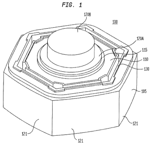
FIG. 1 is a perspective view illustrating an exemplary first diode 100
embodiment.
FIG. 2 is a top view illustrating the exemplary first diode 100 embodiment.
FIG. 3 is a cross-
sectional view (through the 10-10' plane of FIG. 2) illustrating the exemplary
first diode 100
embodiment. FIG. 4 is a perspective view illustrating an exemplary second
diode 100A
embodiment. FIG. 5 is a top view illustrating the exemplary second diode 100A
embodiment.
FIG. 6 is a perspective view illustrating an exemplary third diode 100B
embodiment. FIG. 7 is a
top view illustrating the exemplary third diode 100B embodiment. FIG. 8 is a
perspective view
illustrating an exemplary fourth diode 100C embodiment. FIG. 9 is a top view
illustrating the
exemplary fourth diode 100C embodiment. FIG. 10 is a cross-sectional view
(through the 20-20'
plane of FIGs. 5, 7, 9) illustrating exemplary second, third and/or fourth
diode 100A, 100B,
100C embodiments. FIG. ibis a perspective view illustrating exemplary fifth
and sixth diode
CA 02810394 2013-03-04
WO 2012/031178 PCT/US2011/050292
21
100D, 100E embodiments. FIG. 12 is a top view illustrating the exemplary fifth
and sixth diode
100D, 100E embodiments. FIG. 13 is a cross-sectional view (through the 40-40'
plane of FIG.
12) illustrating the exemplary fifth diode 100D embodiment. FIG. 14 is a cross-
sectional view
(through the 40-40' plane of FIG. 12) illustrating the exemplary sixth diode
100E embodiment.
FIG. 15 is a perspective view illustrating an exemplary seventh diode 100F
embodiment. FIG.
16 is a top view illustrating the exemplary seventh diode 100F embodiment.
FIG. 17 is a cross-
sectional view (through the 42-42' plane of FIG. 16) illustrating the
exemplary seventh diode
100F embodiment. FIG. 18 is a perspective view illustrating an exemplary
eighth diode 100G
embodiment. FIG. 19 is a top view illustrating the exemplary eighth diode 100G
embodiment.
FIG. 20 is a cross-sectional view (through the 43-43' plane of FIG. 19)
illustrating the exemplary
eighth diode 100G embodiment. Cross-sectional views of ninth, tenth and
eleventh diode 100H,
1001, and 100J embodiments are illustrated in FIGs. 39, 45, and 48,
respectively, as part of
illustrations of exemplary fabrication processes. FIG. 63 is a scanning
electron micrograph of an
exemplary second diode 100A embodiment. FIG. 64 is a scanning electron
micrograph of a
plurality of exemplary second diode 100A embodiments.
In the perspective and top view diagrams, FIGs. 1, 2, 4 - 9, 11, 12, 15, 16,
18 and
19, illustration of a passivation layer 135 has been omitted in order to
provide a view of other
underlying layers and structures which would otherwise be covered by such a
passivation layer
135 (and therefore not visible). The passivation layer 135 is illustrated in
the cross-sectional
views of FIGs. 3, 10, 13, 14, 17, 20, 39, 45, and 48, and those having skill
in the electronic arts
will recognize that fabricated diodes 100 - 100J generally will include at
least one such
passivation layer 135. In addition, referring to FIGs. 1 - 48, 52, and 54 -
58, those having skill
in the art will also recognize that the various Figures are for purposes of
description and
explanation, and are not drawn to scale.
As described in greater detail below, the exemplary first through eleventh
diode
embodiments 100 - 100J differ primarily in the shapes, materials, doping and
other compositions
of the substrates 105 and wafers 150, 150A which may be utilized, the
fabricated shape of the
light emitting region of the diode, the depth and locations of vias (130, 131,
132, 133, 134) (such
as shallow or "blind", deep or "through", center, peripheral, and perimeter),
the use of back-side
(second side) metallization (122) to form a second terminal 127, the shapes,
extent and locations
of other contact metals, and may also differ in the shapes or locations of
other features, as
described in greater detail below. Exemplary methods and method variations for
fabricating the
exemplary diodes 100 - 100J are also described below. One or more of the
exemplary diodes
CA 02810394 2013-03-04
WO 2012/031178 PCT/US2011/050292
22
100 ¨ 100J are also available from and may be obtained through NthDegree
Technologies
Worldwide, Inc. of Tempe, Arizona, USA.
Referring to FIGs. 1 ¨ 20, exemplary diodes 100, 100A, 100B, 100C are formed
using a substrate 105, such as a heavily-doped n+ (n plus) or p+ (p plus)
substrate 105, e.g., a
heavily doped n+ or p+ silicon substrate, which may be a silicon wafer or may
be a more
complex substrate or wafer, such as comprising a silicon substrate (105) on
insulator ("SOF), or
a gallium nitride (GaN) substrate 105 on a sapphire (106) wafer 150A
(illustrated in FIGs. 11 ¨
20), for example and without limitation. Other types of substrates (and/or
wafers forming or
having a substrate) 105 may also be utilized equivalently, including Ga, GaAs,
GaN, SiC, 5i02,
sapphire, organic semiconductor, etc., for example and without limitation, and
as discussed in
greater detail below. Accordingly, reference to a substrate 105 should be
understood broadly to
also include any types of substrates, such as n+ or p+ silicon, n+ or p+ GaN,
such as a n+ or p+
silicon substrate formed using a silicon wafer 150 or the n+ or p+ GaN
fabricated on a sapphire
wafer 105A (described below with reference to FIGs. 11 ¨ 20 and 33 ¨ 45). When
embodied
using silicon, the substrate 105 typically has a <111> or <110> crystal
structure or orientation,
although other crystalline structures may be utilized equivalently. An
optional buffer layer 145 is
typically fabricated on a silicon substrate 105, such as aluminum nitride or
silicon nitride, to
facilitate subsequent fabrication of GaN layers having a different lattice
constant. GaN layers are
fabricated over the buffer layer 145, such as through epitaxial growth, to
form a complex GaN
heterostructure, generally illustrated as n+ GaN layer 110, quantum well
region 185, and p+ GaN
layer 115. In other embodiments, a buffer layer 145 is not or may not be
utilized, such as when a
complex GaN heterostructure (n+ GaN layer 110, quantum well region 185, and p+
GaN layer
115) is fabricated over a GaN substrate 105, as illustrated in FIGs. 15 ¨ 17
as a more specific
option. Those having skill in the electronic arts will understand that there
may by many quantum
wells within and potentially multiple p+ and n+ GaN layers to form a light
emitting (or light
absorbing) region 140, with n+ GaN layer 110, quantum well region 185, and p+
GaN layer 115
being merely illustrative and providing a generalized or simplified
description of a complex GaN
heterostructure forming one or more light emitting (or light absorbing)
regions 140. Those
having skill in the electronic arts will also understand that the locations of
the n+ GaN layer 110
and p+ GaN layer 115 may be the same or may be reversed equivalently, such as
for use of a p+
silicon substrate 105, and that other compositions and materials may be
utilized to form one or
more light emitting (or light absorbing) regions 140 (many of which are
described below), and all
such variations are within the scope of the disclosure.
CA 02810394 2013-03-04
WO 2012/031178 PCT/US2011/050292
23
The n+ or p+ substrate 105 conducts current, which flows to the n+ GaN layer
110. The current flow path is also through a metal layer forming one or more
vias 130 (which
may also be utilized to provide an electrical bypass of a very thin (about 25
Angstroms) buffer
layer 145 between the n+ or p+ substrate 105 and the n+ GaN layer 110).
Additional types of
vias 131 ¨ 134 are described below. One or more metal layers 120, illustrated
as two (or more)
separately deposited metal layers 120A and 120B (which also may be used to
form vias 130)
provides an ohmic contact with the p+ GaN layer 115, with the second
additional metal layer
120B utilized to form a "bump" or protruding structure, with metal layers
120A, 120B forming a
first electrical terminal (or contact) 125 for a diode 100 ¨ 100J. For the
illustrated exemplary
diode 100, 100A, 100B, 100C embodiments, electrical terminal 125 may be the
only ohmic,
metallic terminal formed on the diodes 100, 100A, 100B, 100C during
fabrication for subsequent
power (voltage) delivery (for LED applications) or reception (for photovoltaic
applications), with
the n+ or p+ substrate 105 utilized to provide the second electrical terminal
for a diode 100,
100A, 100B, 100C for power delivery or reception. It should be noted that
electrical terminal
125 and the n+ or p+ substrate 105 are on opposing sides, top (first side) and
bottom (or back,
second side) respectively, and not on the same side, of a diode 100, 100A,
100B, 100C. As an
option for these diode 100, 100A, 100B, 100C embodiments and as illustrated
for other
exemplary diode embodiments, an optional, second ohmic, metallic terminal 127
is formed using
metallic layer 122 on the second, back side of a diode (e.g., diode 100D,
100F, 100G, 100J).
Silicon nitride passivation 135 (or any other equivalent passivation) is
utilized, among other
things, for electrical insulation and environmental stability. Not separately
illustrated, a plurality
of trenches 155 were formed during fabrication along the lateral sides of the
diodes 100 ¨ 100J,
as discussed below, which are utilized both to separate the diodes 100 ¨ 100J
from each other on
a wafer 150, 150A, and to separate the diodes 100 ¨ 100J from the remainder of
the wafer 150,
150A.
FIGs. 1 ¨ 20 also illustrate some of the various shapes and form factors of
the one
or more light emitting (or light absorbing) regions 140, illustrated as a GaN
heterostructure (n+
GaN layer 110, quantum well region 185, and p+ GaN layer 115) and the various
shapes and
form factors of the substrate 105. Also as illustrated, while an exemplary
diode 100 ¨ 100J is
substantially hexagonal in the x-y plane (with curved or arced lateral sides
121, concave or
convex, as discussed in greater detail below), to provide greater device
density per silicon wafer,
other diode shapes and forms are considered equivalent and within the scope of
the claimed
invention, such as square, triangular, octagonal, circular, etc. Also as
illustrated in the exemplary
CA 02810394 2013-03-04
WO 2012/031178 PCT/US2011/050292
24
embodiments, the hexagonal lateral sides 121 may also be curved or arced
slightly, convex
(FIGs. 1, 2, 4, 5, 11, 12, 15, 16, 18, 19), concave (FIGs. 6 ¨ 9), such that
when released from the
wafer and suspended in liquid, the diodes 100 ¨ 100J may avoid adhering or
sticking to one
another, and also for apparatus 300, 300A, 300B fabrication, to prevent
individual die (individual
diodes 100 ¨ 100J) from standing on their lateral sides or edges (121). Also
as illustrated in the
exemplary embodiments, the hexagonal lateral sides 121 may also be curved or
arced slightly, to
be both convex about the center of each side 121 and concave
peripherally/laterally to form
somewhat pointed vertices (FIGs. 11 ¨ 20), such that when released from the
wafer and
suspended in liquid, the diodes 100 ¨ 100J also may avoid adhering or sticking
to one another
and may push off one another when rolling or moving against another diode),
and again, also for
apparatus 300, 300A, 300B fabrication, to prevent individual die (individual
diodes 100 ¨ 100J)
from standing on their lateral sides or edges (121).
Various shapes and form factors of the light emitting (or light absorbing)
regions
140 (n+ GaN layer 110, quantum well region 185 and p+ GaN layer 115) are also
illustrated,
with FIGs. 1 ¨ 3 illustrating a substantially circular or disk-shaped light
emitting (or light
absorbing) region 140 (n+ GaN layer 110, quantum well region 185 and p+ GaN
layer 115), and
with FIGs. 4 and 5 illustrating a substantially torus-shaped (or toroidal)
light emitting (or light
absorbing) region 140 (n+ GaN layer 110, quantum well region 185 and p+ GaN
layer 115) with
the second metal layer 120B extending into the center of the toroid (and
potentially providing a
reflective surface). In FIGs. 6 and 7, the light emitting (or light absorbing)
region 140 (n+ GaN
layer 110, quantum well region 185 and p+ GaN layer 115) has a substantially
circular inner
(lateral) surface and a substantially lobed outer (lateral) surface, while in
FIGs. 8 and 9, the light
emitting (or light absorbing) region 140 (n+ GaN layer 110, quantum well
region 185 and p+
GaN layer 115) also has a substantially circular inner (lateral) surface while
the outer (lateral)
surface is substantially stellate- or star-shaped. In FIGs. 11 ¨ 20, the one
or more light emitting
(or light absorbing) regions 140 have a substantially hexagonal (lateral)
surface (which may or
may not extend to the perimeter of the die) and may have (at least partially)
a substantially
circular inner (lateral) surface. In other exemplary embodiments not
separately illustrated, there
may be multiple light emitting (or light absorbing) regions 140, which may be
continuous or
which may be spaced apart on the die. These various configurations of the one
or more light
emitting (or light absorbing) regions 140 (n+ GaN layer 110, quantum well
region 185 and p+
GaN layer 115) having a circular inner surface may be implemented to increase
the potential for
light output (for LED applications) and light absorption (for photovoltaic
applications).
CA 02810394 2013-03-04
WO 2012/031178 PCT/US2011/050292
25
In an exemplary embodiment, the terminal 125 comprised of one or more metal
layers 120A, 120B has a bump or protruding structure, to allow a significant
portion of a diode
100 ¨ 100J to be covered by one or more insulating layers (following formation
of an electrical
contact to the n+ or p+ silicon substrate 105 (or to a second terminal formed
by metal layer 122)
by a first conductor 310A), while simultaneously providing sufficient
structure for contact with
the electrical terminal 125 by one or more other conductive layers, such as a
transparent
conductor 320 discussed below. In addition, the bump or protruding structure
of terminal 125
potentially may also be a factor affecting rotation of a diode 100 ¨ 100J
within the diode ink and
its subsequent orientation (top up (forward bias) or bottom up (reverse bias))
in a fabricated
apparatus 300, 300A, 300B, in addition to the curvature of the lateral sides
121.
Referring to FIGs. 11 ¨ 20, exemplary diodes 100D, 100E, 100F, 100G, in
various
combinations, illustrate several additional and optional features. As
illustrated, metal layer 120B
forming a bump or protruding structure is substantially elliptical (or oval)
in its circumference
rather than substantially circular in circumference, although other shapes and
form factors of the
terminal 125 are also within the scope of the disclosure. In addition, the
metal layer 120B
forming a bump or protruding structure has two or more elongated extensions
124, which serve
several additional purposes in apparatus 300, 300A, 300B fabrication, such as
facilitating
electrical contact formation with a second, transparent conductor 320 and
facilitating flow of an
insulating dielectric 315 off of the terminal 125 (metal layer 120B). The
elliptical form factor
also may allow for additional light emission (or absorption) from or to light
emitting (or light
absorbing) region 140 along the major axis sides of the elliptical metal layer
120B forming a
bump or protruding structure. Metal layer 120A, forming an ohmic contact with
p+ GaN layer
115, which also may be deposited as multiple layers in multiple steps, also
has elongated
extensions over p+ GaN layer 115, illustrated as curved metal contact
extensions 126, facilitating
current conduction to the p+ GaN layer 115 while simultaneously allowing for
(and not blocking
excessively) the potential for light emission or light absorption by the light
emitting (or light
absorbing) regions 140. Innumerable other shapes of the metal contact
extensions 126 may be
utilized equivalently, such as a grid pattern, other curvilinear shapes, etc.
Additional types of via structures (131, 132, 133, 134) are also illustrated
in FIGs.
11 ¨ 20, in addition to the peripheral (i.e., off center), comparatively
shallow or "blind" via 130
previously described which extends through the buffer layer 145 and into the
substrate 105 but
not comparatively deeply into or through the substrate 105 in the fabricated
diode 100, 100A,
100B, 100C. As illustrated in FIG. 13 (and FIGs. 39, 48), a center (or
centrally located),
CA 02810394 2013-03-04
WO 2012/031178 PCT/US2011/050292
26
comparatively deep, "through" via 131 extends completely through the substrate
105, and is
utilized to make an ohmic contact with the n+ GaN layer 110 and to conduct
current (or
otherwise make an electrical contact) between the second (back) side metal
layer 122 and the n+
GaN layer 110. As illustrated in FIG. 14, a center (or centrally located),
comparatively shallow
or blind via 132, also referred to as a "blind" via 132, extends through a
buffer layer 145 and into
the substrate 105, and it utilized to make an ohmic contact with the n+ GaN
layer 110 and to
conduct current (or otherwise make an electrical contact) between the n+ GaN
layer 110 and the
substrate 105. As illustrated in FIGs. 15 - 17 and 44 - 45, a perimeter,
comparatively deep or
through via 133 extends along the lateral sides 121 (although covered by
passivation layer 135)
from the n+ GaN layer 110 and to the second, back-side of the diode 100F,
which in this
embodiment also includes second (back) side metal layer 122, completely around
the lateral sides
of the substrate 105, and it utilized to make an ohmic contact with the n+ GaN
layer 110 and to
conduct current (or otherwise make an electrical contact) between the second
(back) side metal
layer 122 and the n+ GaN layer 110. As illustrated in FIGs. 18 -20, a
peripheral, comparatively
deep, through via 134 extends completely through the substrate 105, and it
utilized to make an
ohmic contact with the n+ GaN layer 110 and to conduct current (or otherwise
make an electrical
contact) between the second (back) side metal layer 122 and the n+ GaN layer
110. In
embodiments which do not utilize a second (back) side metal layer 122, such
through via
structures (131, 133, 134) may be utilized to make an electrical contact with
the conductor 310A
(in an apparatus 300, 300A, 300B) and to conduct current (or otherwise make an
electrical
contact) between the conductor 310A and the n+ GaN layer 110. These through
via structures
(131, 133, 134) are exposed on the second, back side of a diode 110D, 100F,
100G during
fabrication, following singulation of the diodes through either a back side
grind and polish or
laser lift off (discussed below with reference to FIGs. 46 and 47), and may be
left exposed or
may be covered by (and form an electrical contact with) second (back) side
metal layer 122 (as
illustrated in FIG. 48).
The through via structures (131, 133, 134) are considerably narrower than
typical
vias known in the art. The through via structures (131, 133, 134) are on the
order of about 7 -9
microns deep (height extending through the substrate 105) and about 3 - 5
microns wide,
compared to about a 30 micron or greater width of traditional vias.
An optional second (back) side metal layer 122, forming a second terminal or
contact 127, is also illustrated in FIGs. 11 - 13, 17, 18, 20 and 48. Such a
second terminal or
contact 127, for example and without limitation, may be utilized to facilitate
current conduction
CA 02810394 2013-03-04
WO 2012/031178 PCT/US2011/050292
27
to the n+ GaN layer 110, such as through the various through via structures
(131, 133, 134),
and/or to facilitate forming an electrical contact with the conductor 310A.
The diodes 100 ¨ 100J are generally less than about 450 microns in all
dimensions, and more specifically less than about 200 microns in all
dimensions, and more
specifically less than about 100 microns in all dimensions, and more
specifically less than 50
microns in all dimensions. In the illustrated exemplary embodiments, the
diodes 100 ¨ 100J are
generally on the order of about 15 to 40 microns in width, or more
specifically about 20 to 30
microns in width, and about 10 to 15 microns in height, or from about 25 to 28
microns in
diameter (measured side face to face rather than apex to apex) and 10 to 15
microns in height. In
exemplary embodiments, the height of the diodes 100 ¨ 100J excluding the metal
layer 120B
forming the bump or protruding structure (i.e., the height of the lateral
sides 121 including the
GaN heterostructure) is on the order of about 5 to 15 microns, or more
specifically 7 to 12
microns, or more specifically 8 to 11 microns, or more specifically 9 to 10
microns, or more
specifically less than 10 to 30 microns, while the height of the metal layer
120B forming the
bump or protruding structure is generally on the order of about 3 to 7
microns. As the
dimensions of the diodes are engineered to within a selected tolerance during
device fabrication,
the dimensions of the diodes may be measured, for example, using a light
microscope (which
may also include measuring software). As additional examples, the dimensions
of the diodes
may be measured using, for example, a scanning electron microscope (SEM), or
Horiba's LA-
920. The Horiba LA-920 instrument uses the principles of low-angle Fraunhofer
Diffraction and
Light Scattering to measure the particle size and distribution in a dilute
solution of particles, such
as when embodied in a diode ink. All particle sizes are measured in terms of
their number
average particle diameters.
The diodes 100 ¨ 100J may be fabricated using any semiconductor fabrication
techniques which are known currently or which are developed in the future.
FIGs. 21 ¨ 48
illustrate a plurality of exemplary methods of fabricating exemplary diodes
100 ¨ 100J and
illustrate several additional exemplary diodes 100H, 1001 and 100J (in cross-
section). Those
having skill in the art will recognize that many of the various steps of diode
100 ¨ 100J
fabrication may occur in any of various orders, may be omitted or included in
other sequences,
and may result in innumerable diode structures, in addition to those
illustrated. For example,
FIGs. 33 ¨ 39 illustrate creation of a diode 100H which includes both central
and peripheral
through (or deep) vias 131 and 134, respectively, combining features of diodes
100D and 100G,
with or without optional second (back) side metal layer 122, while FIGs. 40 ¨
45 illustrate
CA 02810394 2013-03-04
WO 2012/031178 PCT/US2011/050292
28
creation of a diode 1001 which includes a perimeter via 133, with or without
optional second
(back) side metal layer 122, and which may be combined with the other
illustrated fabrication
steps to include central or peripheral through vias 131 and 134, for example,
such as to form a
diode 100F.
FIGs. 21, 22 and 24 ¨ 32 are cross-sectional views illustrating an exemplary
method of diode 100, 100A, 100B, 100C fabrication in accordance with the
teachings of the
present invention, with FIGs. 21 ¨ 24 illustrating fabrication at the wafer
150 level and FIGs. 25
¨ 32 illustrating fabrication at the diode 100, 100A, 100B, 100C level. FIG.
21 and FIG. 22 are
cross-sectional views of a wafer 150 (such as a silicon wafer) having a
silicon dioxide (or
"oxide") layer 190. FIG. 23 is a top view of a silicon wafer 150 having a
silicon dioxide layer
190 etched in a grid pattern. The oxide layer 190 (generally about 0.1 microns
thick) is deposited
or grown over the wafer 150, as shown in FIG. 21. As illustrated in FIG. 22,
through appropriate
or standard mask and/or photoresist layers and etching as known in the art,
portions of the oxide
layer 190 have been removed, leaving oxide 190 in a grid pattern (also
referred to as "streets"),
as illustrated in FIG. 23.
FIG. 24 is a cross-sectional view of a wafer 150 (such as a silicon wafer)
having a
buffer layer 145, a silicon dioxide (or "oxide") layer 190, and GaN layers
(typically epitaxially
grown or deposited to a thickness of about 1.25 ¨ 2.50 microns in an exemplary
embodiment,
although lesser or greater thicknesses are also within the scope of the
disclosure), illustrated as
polycrystalline GaN 195 over the oxide 190, and n+ GaN layer 110, quantum well
region 185
and p+ GaN layer 115 forming a complex GaN heterostructure as mentioned above.
As indicated
above, a buffer layer 145 (such as aluminum nitride or silicon nitride and
generally about 25
Angstroms thick) is deposited on the silicon wafer 150 to facilitate
subsequent GaN deposition.
The polycrystalline GaN 195 grown or deposited over the oxide 190 is utilized
to reduce the
stress and/or strain (e.g., due to thermal mismatch of the GaN and a silicon
wafer) in the complex
GaN heterostructure (n+ GaN layer 110, quantum well region 185 and p+ GaN
layer 115), which
typically has a single crystal structure. Other equivalent methods within the
scope of the
invention to provide such stress and/or strain reduction, for example and
without limitation,
include roughening the surface of the silicon wafer 150 and/or buffer layer
145 in selected areas,
so that corresponding GaN regions will not be a single crystal, or etching
trenches in the silicon
wafer 150, such that there is also no continuous GaN crystal across the entire
wafer 150. Such
street formation and stress reduction fabrication steps may be omitted in
other exemplary
fabrication methods, such as when other substrates are utilized, such as GaN
(a substrate 105) on
WO 2012/031178 CA 02810394 2013-03-04 PCT/US2011/050292
29
a sapphire wafer 150A. The GaN deposition or growth to form a complex GaN
heterostructure
may be provided through any selected process as known or becomes known in the
art and/or may
be proprietary to the device fabricator. In an exemplary embodiment, the
complex GaN
heterostructure comprised of n+ GaN layer 110, quantum well region 185 and p+
GaN layer 115
has been fabricated by Blue Photonics Inc. of Walnut, California, USA.
FIG. 25 is a cross-sectional view of a substrate 105 having buffer layer 145
and
the complex GaN heterostructure (n+ GaN layer 110, quantum well region 185 and
p+ GaN layer
115) in accordance with the teachings of the present invention, illustrating a
much smaller
portion of the wafer 150 (such as region 191 of FIG. 24), to illustrate
fabrication of a single diode
100, 100A, 100B, 100C. Through appropriate or standard mask and/or photoresist
layers and
etching as known in the art, the complex GaN heterostructure (n+ GaN layer
110, quantum well
region 185 and p+ GaN layer 115) is etched to form a GaN mesa structure 187,
as illustrated in
FIGs. 26 and 27, with FIG. 27 illustrating the GaN mesa structure 187A having
comparatively
more angled sides, which potentially may facilitate light production and/or
absorption. Other
GaN mesa structures 187 may also be implemented, such as a partially or
substantially toroidal
GaN mesa structure 187, as illustrated in FIGs. 10, 13, 14, 17, 20, 34 ¨ 39,
and 48. Following the
GaN mesa etch, also through appropriate or standard mask and/or photoresist
layers and etching
as known or becomes known in the art, a (shallow or blind) via etch is
performed, as illustrated in
FIG. 28, creating a comparatively shallow trench 186 through the GaN layers
and buffer layer
145 and into the silicon substrate 105.
Also through appropriate or standard mask and/or photoresist layers and
etching
as known in the art, metallization layers are then deposited, forming a metal
contact 120A to p+
GaN layer 115 and forming vias 130, as illustrated in FIG. 29. In exemplary
embodiments,
several layers of metal are deposited, a first or initial layer to form an
ohmic contact to p+ GaN
layer 115, typically comprising two metal layers about 50 to 200 Angstroms
each, of nickel
followed by gold, followed by annealing at about 450-500 C in an oxidizing
atmosphere of
about 20% oxygen and 80% nitrogen, resulting in nickel rising to the top with
a layer of nickel
oxide, and forming a metal layer (as part of 120A) having a comparatively good
ohmic contact
with the p+ GaN layer 115. Another metallization layer may also be deposited,
such as to form
thicker interconnect metal to contour and fully form metal layer 120A (e.g.,
for current
distribution) and to form the vias 130. In another exemplary embodiment
(illustrated in FIGs. 40
¨ 45), the metal contact 120A forming an ohmic contact to p+ GaN layer 115 may
be formed
prior to the GaN mesa etch, followed by the GaN mesa etch, via etch, etc.
Innumerable other
CA 02810394 2013-03-04
WO 2012/031178 PCT/US2011/050292
30
metallization processes and corresponding materials comprising metal layers
120A and 120B are
also within the scope of the disclosure, with different fabrication facilities
often utilizing different
processes and material selections. For example and without limitation, either
or both metal
layers 120A and 120B may be formed by deposition of titanium to form an
adhesion or seed
layer, typically 50 ¨ 200 Angstroms thick, followed by deposition of 2 ¨4
microns of nickel and
a thin layer or "flash" of gold (a "flash" of gold being a layer of about 50 ¨
500 Angstroms
thick), 3 ¨ 5 microns of aluminum, followed by nickel (about 0.5 microns,
physical vapor
deposition or plating) and a "flash" of gold, or by deposition of titanium,
followed by gold,
followed by nickel (typically 3 ¨ 5 microns thick for 120B), followed by gold,
or by deposition
of aluminum followed by nickel followed by gold, etc. In addition, the height
of the metal layer
120B forming a bump or protruding structure may also be varied, typically
between about 3.5 ¨
5.5 microns in exemplary embodiments, depending upon the thickness of the
substrate 105 (e.g.,
about 7 ¨ 8 microns of GaN versus about 10 microns of silicon), for the
resulting diodes 100 ¨
100J to have a substantially uniform height and form factor.
For subsequent singulation of the diodes 100 ¨ 100J from each other and from
the
wafer 150, through appropriate or standard mask and/or photoresist layers and
etching as known
in the art, as illustrated in FIG. 30 and other FIGs. 35 and 43, trenches 155
are formed around the
periphery of each diode 100 ¨ 100J (e.g., also as illustrated in FIGs. 2, 5, 7
and 9). The trenches
155 are generally about 3 ¨ 5 microns wide and 10 ¨ 12 microns deep. Also
using appropriate or
standard mask and/or photoresist layers and etching as known in the art,
nitride passivation layer
135 is then grown or deposited, as illustrated in FIG. 31, generally to a
thickness of about 0.35 ¨
1.0 microns, such as by plasma-enhanced chemical vapor deposition (PECVD) of
silicon nitride,
for example and without limitation, followed by photoresist and etching steps
to remove
unwanted regions of silicon nitride. Through appropriate or standard mask
and/or photoresist
layers and etching as known in the art, metal layer 120B having a bump or
protruding structure is
then formed, typically having a height of 3 ¨ 5 microns tall, as illustrated
in FIG. 32. In an
exemplary embodiment, formation of metal layer 120B is performed in several
steps, using a
metal seed layer, followed by more metal deposition using electroplating or a
lift off process,
removing the resist and clearing the field of the seed layer. Other than
subsequent singulation of
the diodes (in this case diodes 100, 100A, 100B, 100C) from the wafer 150, as
described below,
the diodes 100, 100A, 100B, 100C are otherwise complete, and it should be
noted that these
completed diodes 100, 100A, 100B, 100C have only one metal contact or terminal
on the upper
surface of each diode 100, 100A, 100B, 100C (first terminal 125). As an
option, a second (back)
CA 02810394 2013-03-04
WO 2012/031178 PCT/US2011/050292
31
side metal layer 122 may be fabricated, as described below and as mentioned
above with
reference to other exemplary diodes, such as to form a second terminal 127.
FIGs. 33 ¨ 39 illustrate another exemplary method of diode 100 ¨ 100J
fabrication, with FIG. 33 illustrating fabrication at the wafer 150A level and
FIGs. 34 ¨ 39
illustrating fabrication at the diode 100 ¨ 100J level. FIG. 33 is a cross-
sectional view of a wafer
150A having a substrate 105 and having a complex GaN heterostructure (n+ GaN
layer 110,
quantum well region 185, and p+ GaN layer 115). In this exemplary embodiment,
a
comparatively thick layer of GaN is grown or deposited (to form a substrate
105) on sapphire
(106) (of the sapphire wafer 150A), followed by deposition or growth of the
GaN heterostructure
(n+ GaN layer 110, quantum well region 185, and p+ GaN layer 115).
FIG. 34 is a cross-sectional view of a substrate 105 having a third mesa-
etched
complex GaN heterostructure, illustrating a much smaller portion of the wafer
150A (such as
region 192 of FIG. 33), to illustrate fabrication of a single diode (e.g.,
diode 100H). Through
appropriate or standard mask and/or photoresist layers and etching as known in
the art, the
complex GaN heterostructure (n+ GaN layer 110, quantum well region 185 and p+
GaN layer
115) is etched to form a GaN mesa structure 187B. Following the GaN mesa etch,
also through
appropriate or standard mask and/or photoresist layers and etching as known or
becomes known
in the art, a (through or deep) via trench and a singulation trench etch is
performed, as illustrated
in FIG. 35, creating one or more comparatively deep via trenches 188 through
the non-mesa
portion of the GaN heterostructure (n+ GaN layer 110) and though the GaN
substrate 105 to the
sapphire (106) of the wafer 150A and creating singulation trenches 155
described above. As
illustrated, a center via trench 188 and a plurality of peripheral via
trenches 188 have been
formed.
Also through appropriate or standard mask and/or photoresist layers and
etching
as known in the art, metallization layers are then deposited, forming a center
through via 131 and
a plurality of peripheral through vias 134, which also form an ohmic contact
with the n+ GaN
layer 110, as illustrated in FIG. 36. In exemplary embodiments, several layers
of metal are
deposited to form the through vias 131, 134. For example, titanium and
tungsten may be
sputtered to coat the sides and bottom of the trenches 188, to form a seed
layer, followed by
plating with nickel, to form solid metal vias 131, 134.
Also through appropriate or standard mask and/or photoresist layers and
etching
as known in the art, metallization layers are then deposited, forming a metal
layer 120A
providing an ohmic contact to p+ GaN layer 115, as illustrated in FIG. 37. In
exemplary
CA 02810394 2013-03-04
WO 2012/031178 PCT/US2011/050292
32
embodiments, several layers of metal may be deposited as previously described
to form metal
layer 120A and an ohmic contact to p+ GaN layer 115. Also using appropriate or
standard mask
and/or photoresist layers and etching as known in the art, nitride passivation
layer 135 is then
grown or deposited, as illustrated in FIG. 38, generally to a thickness of
about 0.35 ¨ 1.0
microns, such as by plasma-enhanced chemical vapor deposition (PECVD) of
silicon nitride or
silicon oxynitride, for example and without limitation, followed by
photoresist and etching steps
to remove unwanted regions of silicon nitride. Through appropriate or standard
mask and/or
photoresist layers and etching as known in the art, metal layer 120B having a
bump or protruding
structure is then formed, as illustrated in FIG. 39. In an exemplary
embodiment, formation of
metal layer 120B is performed in several steps, using a metal seed layer,
followed by more metal
deposition using electroplating or a lift off process, removing the resist and
clearing the field of
the seed layer, also as described above. Other than subsequent singulation of
the diodes (in this
case diode 100H) from the wafer 150A, as described below, the diodes 100H are
otherwise
complete, and it should be noted that these completed diodes 100H also have
only one metal
contact or terminal on the upper surface of each diode 100H (also a first
terminal 125). Also as
an option, a second (back) side metal layer 122 may be fabricated, as
described below and as
mentioned above with reference to other exemplary diodes, such as to form a
second terminal
127.
FIGs. 40 ¨45 illustrate another exemplary method of diode 100 ¨ 100J
fabrication, with FIG. 40 illustrating fabrication at the wafer 150 or 150A
level and FIGs. 41 ¨ 45
illustrating fabrication at the diode 100 ¨ 100J level. FIG. 40 is a cross-
sectional view of a
substrate 105 having a buffer layer 145, a complex GaN heterostructure (n+ GaN
layer 110,
quantum well region 185, and p+ GaN layer 115), and metallization (metal layer
120A) forming
an ohmic contact with the p+ GaN layer. As mentioned above, buffer layer 145
is typically
fabricated when the substrate 105 is silicon (e.g., using a silicon wafer
150), and may be omitted
for other substrates, such as a GaN substrate 105. In addition, sapphire 106
is illustrated as an
option, such as for a thick GaN substrate 105 grown or deposited on a sapphire
wafer 150A.
Also as mentioned above, a metal layer 119 (as a seed layer for subsequent
deposition of metal
layer 120A) has been deposited at an earlier step, following deposition or
growth of the GaN
heterostructure (n+ GaN layer 110, quantum well region 185, and p+ GaN layer
115), rather than
at a later step of diode fabrication. For example, metal layer 119 may be
nickel with a flash of
gold having a total thickness of about a few hundred Angstroms.
CA 02810394 2013-03-04
WO 2012/031178 PCT/US2011/050292
33
FIG. 41 is a cross-sectional view of a substrate having a buffer layer, a
fourth
mesa-etched complex GaN heterostructure, and metallization (metal layer 119)
forming an ohmic
contact with the p+ GaN layer, illustrating a much smaller portion of the
wafer 150 or 150A
(such as region 193 of FIG. 40), to illustrate fabrication of a single diode
(e.g., diode 1001).
Through appropriate or standard mask and/or photoresist layers and etching as
known in the art,
the complex GaN heterostructure (n+ GaN layer 110, quantum well region 185 and
p+ GaN layer
115) (with metal layer 119) is etched to form a GaN mesa structure 187C (with
metal layer 119).
Following the GaN mesa etch, also through appropriate or standard mask and/or
photoresist
layers as known or becomes known in the art, metallization is deposited (using
any of the
processes and metals previously described, such as titanium and aluminum,
followed by
annealing) to form metal layer 120A and also to form a metal layer 129 having
an ohmic contact
with the n+ GaN layer 110, as illustrated in FIG. 42.
Following the metallization, also through appropriate or standard mask and/or
photoresist layers and etching as known or becomes known in the art, a
singulation trench etch is
performed, as illustrated in FIG. 43, through the non-mesa portion of the GaN
heterostructure (n+
GaN layer 110) and though or comparatively deeply into the substrate 105
(e.g., through the GaN
substrate 105 to the sapphire (106) of the wafer 150A or through part of the
silicon substrate 105
as previously described) and creating singulation trenches 155 described
above.
Also through appropriate or standard mask and/or photoresist layers and
etching
as known in the art, metallization layers are then deposited within trenches
155, forming a
through or deep perimeter via 133 (providing conduction around the entire
outside or lateral
perimeter of the diode (100I), which also form an ohmic contact with the n+
GaN layer 110, as
illustrated in FIG. 44. In exemplary embodiments, several layers of metal also
may be deposited
to form the through perimeter via 133. For example, titanium and tungsten may
be sputtered to
coat the sides and bottom of the trenches 155, to form a seed layer, followed
by plating with
nickel, to form a solid metal perimeter via 133.
Again also using appropriate or standard mask and/or photoresist layers and
etching as known in the art, nitride passivation layer 135 is then grown or
deposited, as illustrated
in FIG. 45, generally to a thickness of about 0.35 ¨ 1.0 microns, such as by
plasma-enhanced
chemical vapor deposition (PECVD) of silicon nitride, for example and without
limitation,
followed by photoresist and etching steps to remove unwanted regions of
silicon nitride.
Through appropriate or standard mask and/or photoresist layers and etching as
known in the art,
metal layer 120B having a bump or protruding structure is then formed as
previously described,
CA 02810394 2013-03-04
WO 2012/031178 PCT/US2011/050292
34
as illustrated in FIG. 45. Other than subsequent singulation of the diodes (in
this case diode
1001) from the wafer 150 or 150A, as described below, the diodes 1001 are
otherwise complete,
and it should be noted that these completed diodes 1001 also have only one
metal contact or
terminal on the upper surface of each diode 1001 (also a first terminal 125).
Also as an option, a
second (back) side metal layer 122 may be fabricated, as described below and
as mentioned
above with reference to other exemplary diodes, such as to form a second
terminal 127.
Numerous variations of the methodology for fabrication of diodes 100 ¨ 100J
may
be readily apparent in light of the teachings of the disclosure, all of which
are considered
equivalent and within the scope of the disclosure. In other exemplary
embodiments, such trench
155 formation and (nitride) passivation layer formation may be performed
earlier or later in the
device fabrication process. For example, trenches 155 may be formed later in
fabrication, after
formation of metal layer 120B, and may leave exposed substrate 105, or may be
followed by a
second passivation. Also for example, trenches 155 may be formed earlier in
fabrication, such as
after the GaN mesa etch, followed by deposition of (nitride) passivation layer
135. In the latter
example, to maintain planarization during the balance of the device
fabrication process, the
passivated trenches 155 may be filled in with oxide, photoresist or other
material (deposition of
the layer followed by removal of unwanted areas using a photoresist mask and
etch or an
unmasked etch process) or may be filled in (and potentially refilled following
metal contact 120A
formation) with resist. In another example, silicon nitride 135 deposition
(followed by mask and
etch steps) may be performed following the GaN mesa etch and before metal
contact 120A
deposition.
It should also be noted that while many of the various diodes (of diodes 100 ¨
100J) have been discussed in which silicon and GaN may be or are the selected
semiconductors,
other inorganic or organic semiconductors may be utilized equivalently and are
within the scope
of the disclosure. Examples of inorganic semiconductors include, without
limitation: silicon,
germanium, and mixtures thereof; titanium dioxide, silicon dioxide, zinc
oxide, indium-tin oxide,
antimony-tin oxide, and mixtures thereof; II-VI semiconductors, which are
compounds of at least
one divalent metal (zinc, cadmium, mercury and lead) and at least one divalent
non-metal
(oxygen, sulfur, selenium, and tellurium) such as zinc oxide, cadmium
selenide, cadmium
sulfide, mercury selenide, and mixtures thereof; III-V semiconductors, which
are compounds of
at least one trivalent metal (aluminum, gallium, indium, and thallium) with at
least one trivalent
non-metal (nitrogen, phosphorous, arsenic, and antimony) such as gallium
arsenide, indium
CA 02810394 2013-03-04
WO 2012/031178 PCT/US2011/050292
35
phosphide, and mixtures thereof; and group IV semiconductors including
hydrogen terminated
silicon, carbon, germanium, and alpha-tin, and combinations thereof.
In addition to the GaN light emitting/absorbing region 140 (e.g., A GaN
heterostructure deposited over a substrate 105 such as n+ or p+ silicon or
deposited over GaN
(105) on a sapphire (106) wafer 150A), the plurality of diodes 100 ¨ 100J may
be comprised of
any type of semiconductor element, material or compound, such as silicon,
gallium arsenide
(GaAs), gallium nitride (GaN), or any inorganic or organic semiconductor
material, and in any
form, including GaP, InAlGaP, InAlGaP, AlinGaAs, InGaNAs, AlInGASb, also for
example and
without limitation.
FIG. 46 is a cross-sectional view illustrating an exemplary silicon wafer 150
embodiment having a plurality of diodes 100 ¨ 100J adhered to a holding
apparatus 160 (such as
a holding, handle or holder wafer). FIG. 47 is a cross-sectional view
illustrating an exemplary
diode sapphire wafer 150A embodiment adhered to a holding apparatus 160. As
illustrated in
FIGs. 46 and 47, the diode wafer 150, 150A containing a plurality of
unreleased diodes 100 ¨
100J (illustrated generally for purposes of explication and without any
significant feature detail)
is adhered, using any known, commercially available wafer adhesive or wafer
bond 165, to a
holding apparatus 160 (such as a wafer holder) on the first side of the diode
wafer 150, 150A
having the fabricated diodes 100 ¨ 100J. As illustrated and as described
above, a nitride
passivated, singulation or individuation trench 155 between each diode 100 ¨
100J, has been
formed during wafer processing, such as through etching, and is then utilized
to separate each
diode 100 ¨ 100J from adjacent diodes 100 ¨ 100J without a mechanical process
such as sawing.
As illustrated in FIG. 46, while the diode wafer 150 is still adhered to the
holding apparatus 160,
the second, backside 180 of the diode wafer 150 is then mechanically ground
and polished to a
level (illustrated as a dashed line) to expose the nitride passivated trenches
155. When
sufficiently ground and polished, each individual diode 100 ¨ 100J has been
released from each
other and any remaining diode wafer 150, while still adhered with the adhesive
165 to the
holding apparatus 160. As illustrated in FIG. 47, also while the diode wafer
150A is still adhered
to the holding apparatus 160, the second, backside 180 of the diode wafer 150A
is then exposed
to laser light (illustrated as one or more laser beams 162) which then cleaves
(illustrated as a
dashed line) the GaN substrate 105 from the sapphire 106 of the wafer 150A
(also referred to as
laser lift-off), thereby releasing each individual diode 100 ¨ 100J from each
other and the wafer
150A, while still adhered with the adhesive 165 to the holding apparatus 160.
In this exemplary
embodiment, the wafer 150A may then be ground and/or polished and re-used.
CA 02810394 2013-03-04
WO 2012/031178 PCT/US2011/050292
36
An epoxy bead (not separately illustrated) is also generally applied about the
periphery of the wafer 150, to prevent non-diode fragments from the edge of
the wafer from
being released into the diode (100 ¨ 100J) fluid during the diode release
process discussed below.
FIG. 48 is a cross-sectional view illustrating an exemplary diode 100J
embodiment adhered to a holding apparatus. Following singulation of the diodes
100 ¨ 100J (as
described above with reference to FIGs. 46 and 47), and while the diodes 100 ¨
100J are still
adhered with adhesive 165 to the holding apparatus 160, the second, back side
of the diode 100 ¨
100J is exposed. As illustrated in FIG. 48, metallization may then be
deposited to the second,
back side, such as through vapor deposition (angled to avoid filling the
trenches 155), forming
second, back side metal layer 122 and a diode 100J embodiment. Also as
illustrated, diode 100J
has one center through via 131 having an ohmic contact with the n+ GaN layer
110 and contact
with the second, back side metal layer 122 for current conduction between the
n+ GaN layer 110
and the second, back side metal layer 122. Exemplary diode 100D is quite
similar, with
exemplary diode 100J having the second, back side metal layer 122 to form a
second terminal
127. As previously mentioned, the second, back side metal layer 122 (or the
substrate 105 or any
of the various through vias 131, 133, 134) may be used to make an electrical
connection with a
first conductor 310 in an apparatus 300, 300A, 300B for energizing the diode
100 ¨ 100J.
FIGs. 49, 50 and 51 are flow diagrams illustrating exemplary first, second and
third method embodiments for diode 100 ¨ 100J fabrication, respectively, and
provide a useful
summary. It should be noted that many of the steps of these methods may be
performed in any of
various orders, and that steps of one exemplary method may also be utilized in
the other
exemplary methods. Accordingly, each of the methods will refer generally to
fabrication of any
of the diodes 100 ¨ 100J, rather than fabrication of a specific diode 100 ¨
100J embodiment, and
those having skill in the art will recognize which steps may be "mixed and
matched" to create
any selected diode 100 ¨ 100J embodiment.
Referring to FIG. 49, beginning with start step 240, an oxide layer is grown
or
deposited on a semiconductor wafer, step 245, such as a silicon wafer. The
oxide layer is etched,
step 250, such as to form a grid or other pattern. A buffer layer and a light
emitting or absorbing
region (such as a GaN heterostructure) is grown or deposited, step 255, and
then etched to form a
mesa structure for each diode 100 ¨ 100J, step 260. The wafer 150 is then
etched to form via
trenches into the substrate 105 for each diode 100 ¨ 100J, step 265. One or
more metallization
layers are then deposited to form a metal contact and vias for each diode 100
¨ 100J, step 270.
Singulation trenches are then etched between diodes 100 ¨ 100J, step 275. A
passivation layer is
CA 02810394 2013-03-04
WO 2012/031178 PCT/US2011/050292
37
then grown or deposited, step 280. A bump or protruding metal structure is
then deposited or
grown on the metal contact, step 285, and the method may end, return step 290.
It should be
noted that many of these fabrication steps may be performed by different
entities and agents, and
that the method may include the other variations and ordering of steps
discussed above.
Referring to FIG. 50, beginning with start step 500, a comparatively thick GaN
layer (e.g., 7 ¨ 8 microns) is grown or deposited on a wafer, step 505, such
as a sapphire wafer
150A. A light emitting or absorbing region (such as a GaN heterostructure) is
grown or
deposited, step 510, and then etched to form a mesa structure for each diode
100 ¨ 100J (on a
first side of each diode 100 ¨ 100J), step 515. The wafer 150 is then etched
to form one or more
through or deep via trenches and singulation trenches into the substrate 105
for each diode 100 ¨
100J, step 520. One or more metallization layers are then deposited to form
through vias for
each diode 100 ¨ 100J, which may be center, peripheral or perimeter through
vias (131, 134, 133,
respectively), typically by depositing a seed layer, step 525, followed by
additional metal
deposition using any of the methods described above. Metal is also deposited
to form one or
more metal contacts to the GaN heterostructure (such as to the p+ GaN layer
115 or to the n+
GaN layer 110), step 535, and to form any additional current distribution
metal (e.g., 120A, 126),
step 540. A passivation layer is then grown or deposited, step 545, with areas
etched or removed
as previously described and illustrated. A bump or protruding metal structure
(120B) is then
deposited or grown on the metal contact(s), step 550. The wafer 150A is then
attached to a
holding wafer, step 555, and the sapphire or other wafer is removed (e.g.,
through laser cleaving)
to singulate or individuate the diodes 100 ¨ 100J, step 560. Metal is then
deposited on the
second, back side of the diodes 100 ¨ 100J to form the second, back side metal
layer 122, step
565, and the method may end, return step 570. It also should be noted that
many of these
fabrication steps may be performed by different entities and agents, and that
the method may
include the other variations and ordering of steps discussed above.
Referring to FIG. 51, beginning with start step 600, a comparatively thick GaN
layer (e.g., 7 ¨ 8 microns) is grown or deposited on a wafer 150, step 605,
such as a sapphire
wafer 150A. A light emitting or absorbing region (such as a GaN
heterostructure) is grown or
deposited, step 610. Metal is deposited to form one or more metal contacts to
the GaN
heterostructure (such as to the p+ GaN layer 115 as illustrated in FIG. 40),
step 615. The light
emitting or absorbing region (such as the GaN heterostructure) with the metal
contact layer (119)
are then etched to form a mesa structure for each diode 100 ¨ 100J (on a first
side of each diode
100 ¨ 100J), step 620. Metal is deposited to form one or more metal contacts
to the GaN
CA 02810394 2013-03-04
WO 2012/031178 PCT/US2011/050292
38
heterostructure (such as n+ metal contact layer 129 to the n+ GaN layer 110 as
illustrated in FIG.
42), step 625. The wafer 150A is then etched to form one or more through or
deep via trenches
and/or singulation trenches into the substrate 105 for each diode 100 ¨ 100J,
step 630. One or
more metallization layers are then deposited to form through vias for each
diode 100 ¨ 100J, step
635, which may be center, peripheral or perimeter through vias (131, 134, 133,
respectively),
using any of the metal deposition methods described above. Metal is also
deposited to form one
or more metal contacts to the GaN heterostructure (such as the p+ GaN layer
115 or to the n+
GaN layer 110), and to form any additional current distribution metal (e.g.,
120A, 126), step 640.
If singulation trenches were not previously created (in step 630), then
singulation trenches are
etched, step 645. A passivation layer is then grown or deposited, step 650,
with areas etched or
removed as previously described and illustrated. A bump or protruding metal
structure (120B) is
then deposited or grown on the metal contact(s), step 655. The wafer 150, 150A
is then attached
to a holding wafer, step 660, and the sapphire or other wafer is removed
(e.g., through laser
cleaving or back side grinding and polishing) to singulate or individuate the
diodes 100 ¨ 100J,
step 665. Metal is then deposited on the second, back side of the diodes 100 ¨
100J to form the
second, back side conductive (e.g., metal) layer 122, step 670, and the method
may end, return
step 675. It also should be noted that many of these fabrication steps may be
performed by
different entities and agents, and that the method may include the other
variations and ordering of
steps discussed above.
FIG. 52 is a cross-sectional view illustrating individual diodes 100 ¨ 100J
(also
illustrated generally for purposes of explication and without any significant
feature detail) which
are no longer coupled together on the diode wafer 150, 150A (as the second
side of the diode
wafer 150, 150A has now been ground or polished or cleaved (laser lift-off) to
fully expose the
singulation (individuation) trenches 155), but which are adhered with wafer
adhesive 165 to a
holding apparatus 160 and suspended or submerged in a dish 175 with wafer
adhesive solvent
170. Any suitable dish 175 may be utilized, such as a petri dish, with an
exemplary method
utilizing a polytetrafluoroethylene (PTFE or Teflon) dish 175. The wafer
adhesive solvent 170
may be any commercially available wafer adhesive solvent or wafer bond
remover, including
without limitation 2-dodecene wafer bond remover available from Brewer
Science, Inc. of Rolla,
Missouri USA, for example, or any other comparatively long chain alkane or
alkene or shorter
chain heptane or heptene. The diodes 100 ¨ 100J adhered to the holding
apparatus 160 are
submerged in the wafer adhesive solvent 170 for about five to about fifteen
minutes, typically at
room temperature (e.g., about 65 F ¨ 75 F or a higher temperature, and may
also be sonicated in
WO 2012/031178 CA 02810394 2013-03-04 PCT/US2011/050292
39
exemplary embodiments. As the wafer adhesive solvent 170 dissolves the
adhesive 165, the
diodes 100 ¨ 100J separate from the adhesive 165 and holding apparatus 160 and
mostly or
generally sink to the bottom of the dish 175, individually or in groups or
clumps. When all or
most diodes 100 ¨ 100J have been released from the holding apparatus 160 and
have settled to
the bottom of the dish 175, the holding apparatus 160 and a portion of the
currently used wafer
adhesive solvent 170 are removed from the dish 175. More wafer adhesive
solvent 170 is then
added (about 120 ¨ 140 ml), and the mixture of wafer adhesive solvent 170 and
diodes 100 ¨
100J is agitated (e.g., using a sonicator or an impeller mixer) for about five
to fifteen minutes,
typically at room or higher temperature, followed by once again allowing the
diodes 100 ¨ 100J
to settle to the bottom of the dish 175. This process is then repeated
generally at least once more,
such that when all or most diodes 100 ¨ 100J have settled to the bottom of the
dish 175, a portion
of the currently used wafer adhesive solvent 170 is removed from the dish 175
and more (about
120 ¨ 140 ml) wafer adhesive solvent 170 is then added, followed by agitating
the mixture of
wafer adhesive solvent 170 and diodes 100 ¨ 100J for about five to fifteen
minutes, at room or
higher temperature, followed by once again allowing the diodes 100 ¨ 100J to
settle to the
bottom of the dish 175 and removing a portion of the remaining wafer adhesive
solvent 170. At
this stage, a sufficient amount of any residual wafer adhesive 165 generally
will have been
removed from the diodes 100 ¨ 100J, or the wafer adhesive solvent 170 process
repeated, to no
longer potentially interfere with the printing or functioning of the diodes
100 ¨ 100J.
Removal of the wafer adhesive solvent 170 (having the dissolved wafer adhesive
165), or of any of the other solvents, solutions or other liquids discussed
below, may be
accomplished in any of various ways. For example, wafer adhesive solvent 170
or other liquids
may be removed by vacuum, aspiration, suction, pumping, etc., such as through
a pipette. Also
for example, wafer adhesive solvent 170 or other liquids may be removed by
filtering the mixture
of diodes 100 ¨ 100J and wafer adhesive solvent 170 (or other liquids), such
as by using a screen
or porous silicon membrane having an appropriate opening or pore size. It
should also be
mentioned that all of the various fluids used in the diode ink (and dielectric
ink discussed below)
are filtered to remove particles larger than about 10 microns.
Diode Ink Example 1:
A composition comprising:
a plurality of diodes 100 ¨ 100J; and
a solvent.
CA 02810394 2013-03-04
WO 2012/031178 PCT/US2011/050292
40
Substantially all or most of the wafer adhesive solvent 170 is then removed. A
solvent, and more particularly a polar solvent such as isopropyl alcohol
("IPA") in an exemplary
embodiment and for example, is added to the mixture of wafer adhesive solvent
170 and diodes
100 ¨ 100J, followed by agitating the mixture of IPA, wafer adhesive solvent
170 and diodes 100
¨ 100J for about five to fifteen minutes, generally at room temperature
(although a higher
temperature may be utilized equivalently), followed by once again allowing the
diodes 100 ¨
100J to settle to the bottom of the dish 175 and removing a portion of the
mixture of IPA and
wafer adhesive solvent 170. More IPA is added (120 ¨ 140 ml), and the process
is repeated two
or more times, namely, agitating the mixture of IPA, wafer adhesive solvent
170 and diodes 100
¨ 100J for about five to fifteen minutes, generally at room temperature,
followed by once again
allowing the diodes 100 ¨ 100J to settle to the bottom of the dish 175,
removing a portion of the
mixture of IPA and wafer adhesive solvent 170 and adding more IPA. In an
exemplary
embodiment, the resulting mixture is about 100-110 ml of IPA with
approximately 9-10 million
diodes 100 ¨ 100J from a four inch wafer (approximately 9.7 million diodes 100
¨ 100J per four
inch wafer 150), and is then transferred to another, larger container, such as
a PTFE jar, which
may include additional washing of diodes into the jar with additional IPA, for
example. One or
more solvents may be used equivalently, for example and without limitation:
water; alcohols
such as methanol, ethanol, N-propanol (including 1-propanol, 2-propanol
(IPA)), butanol
(including 1- butanol, 2- butanol (isobutanol)), pentanol (including 1-
pentanol, 2- pentanol, 3-
pentanol), octanol, tetrahydrofurfuryl alcohol (THFA), cyclohexanol,
terpineol; ethers such as
methyl ethyl ether, diethyl ether, ethyl propyl ether, and polyethers; esters
such ethyl acetate;
glycols such as ethylene glycols, diethylene glycol, polyethylene glycols,
propylene glycols,
glycol ethers, glycol ether acetates; carbonates such as propylene carbonate;
glycerin,
acetonitrile, tetrahydrofuran (THF), dimethyl formamide (DMF), N-methyl
formamide (NMF),
dimethyl sulfoxide (DMS0); and mixtures thereof. The resulting mixture of
diodes 100 ¨ 100J
and a solvent such as IPA is a first example of a diode ink, as Example 1
above, and may be
provided as a stand-alone composition, for example, for subsequent
modification or use in
printing, also for example. In other exemplary embodiments discussed below,
the resulting
mixture of diodes 100 ¨ 100J and a solvent such as IPA is an intermediate
mixture which is
further modified to form a diode ink for use in printing, as described below.
In various exemplary embodiments, the selection of a first (or second) solvent
is
based upon at least two properties or characteristics. A first characteristic
of the solvent is its
CA 02810394 2013-03-04
WO 2012/031178 PCT/US2011/050292
41
ability be soluble in or to solubilize a viscosity modifier or an adhesive
viscosity modifier such as
methoxyl cellulose or hydroxypropyl cellulose resin. A second characteristic
or property is its
evaporation rate, which should be slow enough to allow sufficient screen
residence (for screen
printing) of the diode ink or to meet other printing parameters. In various
exemplary
embodiments, an exemplary evaporation rate is less than one (< 1, as a
relative rate compared
with butyl acetate), or more specifically, between 0.0001 and 0.9999.
Diode Ink Example 2:
A composition comprising:
a plurality of diodes 100 ¨ 100J; and
a viscosity modifier.
Diode Ink Example 3:
A composition comprising:
a plurality of diodes 100 ¨ 100J; and
a solvating agent.
Diode Ink Example 4:
A composition comprising:
a plurality of diodes 100 ¨ 100J; and
a wetting solvent.
Diode Ink Example 5:
A composition comprising:
a plurality of diodes 100 ¨ 100J;
a solvent; and
a viscosity modifier.
Diode Ink Example 6:
A composition comprising:
a plurality of diodes 100 ¨ 100J;
a solvent; and
an adhesive viscosity modifier.
WO 2012/031178 CA 02810394 2013-03-04 PCT/US2011/050292
42
Diode Ink Example 7:
A composition comprising:
a plurality of diodes 100 ¨ 100J;
a solvent; and
a viscosity modifier;
wherein the composition is opaque when wet and substantially clear when
dried.
Diode Ink Example 8:
A composition comprising:
a plurality of diodes 100 ¨ 100J;
a first, polar solvent;
a viscosity modifier; and
a second, nonpolar solvent (or rewetting agent).
Diode Ink Example 9:
A composition comprising:
a plurality of diodes 100 ¨ 100J, each diode of the plurality of diodes 100 ¨
100J having a size less than 450 microns in any dimension; and
a solvent.
Diode Ink Example 10:
A composition comprising:
a plurality of diodes 100 ¨ 100J; and
at least one substantially non-insulating carrier or solvent.
Diode Ink Example 11:
A composition comprising:
a plurality of diodes 100 ¨ 100J;
a solvent; and
a viscosity modifier;
wherein the composition has a dewetting or contact angle greater than 25
degrees, or greater than 40 degrees.
CA 02810394 2013-03-04
WO 2012/031178 PCT/US2011/050292
43
Referring to Diode Ink Examples 1 ¨ 10, there are a wide variety of exemplary
diode ink compositions within the scope of the present invention. Generally,
as in Example 1, a
liquid suspension of diodes (100 ¨ 100J) comprises a plurality of diodes (100
¨ 100J) and a first
solvent (such as IPA discussed above or N-propanol, terpineol or diethylene
glycol discussed
below); as in Examples 2, a liquid suspension of diodes (100 ¨ 100J) comprises
a plurality of
diodes (100 ¨ 100J) and a viscosity modifier (such those discussed below,
which may also be an
adhesive viscosity modifier as in Example 6); and as in Examples 3 and 4, a
liquid suspension of
diodes (100 ¨ 100J) comprises a plurality of diodes (100 ¨ 100J) and a
solvating agent or a
wetting solvent (such as one of the second solvents discussed, below, e.g., a
dibasic ester). More
particularly, such as in Examples 2, 5, 6, 7 and 8, a liquid suspension of
diodes (100 ¨ 100J)
comprises a plurality of diodes (100 ¨ 100J) (and/or plurality of diodes (100
¨ 100J) and a first
solvent (such as N-propanol, terpineol or diethylene glycol)), and a viscosity
modifier (or
equivalently, a viscous compound, a viscous agent, a viscous polymer, a
viscous resin, a viscous
binder, a thickener, and/or a rheology modifier) or an adhesive viscosity
modifier (discussed in
greater detail below), to provide a diode ink having a viscosity between about
1,000 centipoise
(cps) and 20,000 cps at room temperature (about 25 C) (or between about
20,000 cps to 60,000
cps at a refrigerated temperature (e.g., 5-10 C)), such as an E-10 viscosity
modifier described
below, for example and without limitation. Depending upon the viscosity, the
resulting
composition may be referred to equivalently as a liquid or as a gel suspension
of diodes, and any
reference to liquid or gel herein shall be understood to mean and include the
other.
In addition, the resulting viscosity of the diode ink will generally vary
depending
upon the type of printing process to be utilized and may also vary depending
upon the diode
composition, such as a silicon substrate 105 or a GaN substrate 105. For
example, a diode ink
for screen printing in which the diodes 100 ¨ 100J have a silicon substrate
105 may have a
viscosity between about 5,000 centipoise (cps) and 20,000 cps at room
temperature, or more
specifically between about 6,000 centipoise (cps) and 15,000 cps at room
temperature, or more
specifically between about 8,000 centipoise (cps) and 12,000 cps at room
temperature, or more
specifically between about 9,000 centipoise (cps) and 11,000 cps at room
temperature. For
another example, a diode ink for screen printing in which the diodes 100 ¨
100J have a GaN
substrate 105 may have a viscosity between about 10,000 centipoise (cps) and
25,000 cps at
room temperature, or more specifically between about 15,000 centipoise (cps)
and 22,000 cps at
room temperature, or more specifically between about 17,500 centipoise (cps)
and 20,500 cps at
CA 02810394 2013-03-04
WO 2012/031178 PCT/US2011/050292
44
room temperature, or more specifically between about 18,000 centipoise (cps)
and 20,000 cps at
room temperature. Also for example, a diode ink for flexographic printing in
which the diodes
100 ¨ 100J have a silicon substrate 105 may have a viscosity between about
1,000 centipoise
(cps) and 10,000 cps at room temperature, or more specifically between about
1,500 centipoise
(cps) and 4,000 cps at room temperature, or more specifically between about
1,700 centipoise
(cps) and 3,000 cps at room temperature, or more specifically between about
1,800 centipoise
(cps) and 2,200 cps at room temperature. Also for example, a diode ink for
flexographic printing
in which the diodes 100 ¨ 100J have a GaN substrate 105 may have a viscosity
between about
1,000 centipoise (cps) and 10,000 cps at room temperature, or more
specifically between about
2,000 centipoise (cps) and 6,000 cps at room temperature, or more specifically
between about
2,500 centipoise (cps) and 4,500 cps at room temperature, or more specifically
between about
2,000 centipoise (cps) and 4,000 cps at room temperature.
Viscosity may be measured in a wide variety of ways. For purposes of
comparison, the various specified and/or claimed ranges of viscosity herein
have been measured
using a Brookfield viscometer (available from Brookfield Engineering
Laboratories of
Middleboro, Massachusetts, USA) at a shear stress of about 200 pascals (or
more generally
between 190 and 210 pascals), in a water jacket at about 25 C, using a
spindle 5C4-27 at a speed
of about 10 rpm (or more generally between 1 and 30 rpm, particularly for
refrigerated fluids, for
example and without limitation).
One or more thickeners (as a viscosity modifier) may be used, for example and
without limitation: clays such as hectorite clays, garamite clays, organo-
modified clays;
saccharides and polysaccharides such as guar gum, xanthan gum; celluloses and
modified
celluloses such as hydroxyl methyl cellulose, methyl cellulose, methoxyl
cellulose,
carboxymethyl cellulose, hydroxyethyl cellulose and hydroxypropyl cellulose,
cellulose ether,
cellulose ethyl ether, chitosan; polymers such as acrylate and (meth)acrylate
polymers and
copolymers, diethylene glycol, propylene glycol, fumed silica (such as
Cabosil), silica powders
and modified ureas such as BYKC) 420 (available from BYK Chemie GmbH); and
mixtures
thereof. Other viscosity modifiers may be used, as well as particle addition
to control viscosity,
as described in Lewis et al., Patent Application Publication Pub. No. US
2003/0091647. Other
viscosity modifiers discussed below with reference to dielectric inks may also
be utilized, but are
not preferred.
Referring to Diode Ink Example 6, the liquid suspension of diodes (100 ¨ 100J)
may further comprise an adhesive viscosity modifier, namely, any of the
viscosity modifiers
CA 02810394 2013-03-04
WO 2012/031178 PCT/US2011/050292
45
mentioned above which have the additional property of adhesion. Such an
adhesive viscosity
modifier provides for both adhering the diodes (100 ¨ 100J) to a first
conductor (e.g., 310A)
during apparatus (300, 300A, 300B) fabrication (e.g., printing), and then
further provides for an
infrastructure (e.g., polymeric) (when dried or cured) for holding the diodes
(100 ¨ 100J) in place
in an apparatus (300, 300A, 300B). While providing such adhesion, such a
viscosity modifier
should also have some capability to de-wet from the contacts of the diodes
(100 ¨ 100J), such as
the terminals 125 and/or 127. Such adhesive, viscosity and de-wetting
properties are among the
reasons methoxyl cellulose or hydroxypropyl cellulose resins have been
utilized in various
exemplary embodiments. Other suitable viscosity modifiers may also be selected
empirically.
Additional properties of the viscosity modifier or adhesive viscosity modifier
are
also useful and within the scope of the disclosure. First, such a viscosity
modifier should prevent
the suspended diodes (100 ¨ 100J) from settling out at a selected temperature.
Second, such a
viscosity modifier should aid in orienting the diodes (100 ¨ 100J) and
printing the diodes (100 ¨
100J) in a uniform manner during apparatus (300, 300A, 300B) fabrication.
Third, the viscosity
modifier should also serve to cushion or otherwise protect the diodes (100 ¨
100J) during the
printing process.
Referring to Diode Ink Examples 3, 4 and 8, the liquid suspension of diodes
(100
¨ 100J) may further comprise a second solvent (Example 8) or a solvating agent
(Example 3) or a
wetting solvent (Example 4), with many examples discussed in greater detail
below. Such a (first
or second) solvent is selected as a wetting (equivalently, solvating) or
rewetting agent for
facilitating ohmic contact between a first conductor (e.g., 310A, which may be
comprised of a
conductive polymer such as a silver ink, a carbon ink, or mixture of silver
and carbon ink) and
the diodes 100 ¨ 100J (through the substrate 105, a through via structures
(131, 133, 134), and/or
a second, back side metal layer 122, as illustrated in FIG. 58), following
printing and drying of
the diode ink during subsequent device manufacture, such as a nonpolar resin
solvent, including
one or more dibasic esters, also for example and without limitation. For
example, when the
diode ink is printed over a first conductor 310, the wetting or solvating
agent partially dissolves
the first conductor 310; as the wetting or solvating agent subsequently
dissipates, the first
conductor 310 re-hardens and forms a contact with the diodes (100¨ 100J).
The balance of the liquid or gel suspension of diodes (100 ¨ 100J) is
generally
another, third solvent, such as deionized water, and any descriptions of
percentages herein shall
assume that the balance of the liquid or gel suspension of diodes (100 ¨ 100J)
is such a third
solvent such as water, and all described percentages are based on weight,
rather than volume or
CA 02810394 2013-03-04
WO 2012/031178 PCT/US2011/050292
46
some other measure. It should also be noted that the various diode ink
suspensions may all be
mixed in a typical atmospheric setting, without requiring any particular
composition of air or
other contained or filtered environment.
Solvent selection may also be based upon the polarity of the solvent. In an
exemplary embodiment, a first solvent such as an alcohol may be selected as a
polar or
hydrophilic solvent, to facilitate de-wetting off of the diodes (100 ¨ 100J)
and other conductors
(e.g., 310) during apparatus 300, 300A, 300B fabrication, while concomitantly
being able to be
soluble in or solubilize a viscosity modifier.
Another useful property of an exemplary diode ink is illustrated by Example 7.
For this exemplary embodiment, the diode ink is opaque when wet during
printing, to aid in
various printing processes such as registration. When dried or cured, however,
the dried or cured
diode ink is substantially clear at selected wavelengths, such as clear to
substantially allow or not
interfere with the emission of visible light generated by the diodes (100 ¨
100J).
Another way to characterize an exemplary diode ink is based upon the size of
the
diodes (100 ¨ 100J), as illustrated by Example 7, in which the diodes 100 ¨
100J are generally
less than about 450 microns in any dimension, and more specifically less than
about 200 microns
in any dimension, and more specifically less than about 100 microns in any
dimension, and more
specifically less than 50 microns in any dimension. In the illustrated
exemplary embodiments,
the diodes 100 ¨ 100J are generally on the order of about 15 to 40 microns in
width, or more
specifically about 20 to 30 microns in width, and about 10 to 15 microns in
height, or from about
to 28 microns in diameter (measured side face to face rather than apex to
apex) and 10 to 15
microns in height. In exemplary embodiments, the height of the diodes 100 ¨
100J excluding the
metal layer 120B forming the bump or protruding structure (i.e., the height of
the lateral sides
121 including the GaN heterostructure) is on the order of about 5 to 15
microns, or more
25 specifically 7 to 12 microns, or more specifically 8 to 11 microns, or more
specifically 9 to 10
microns, or more specifically less than 10 to 30 microns, while the height of
the metal layer 120B
forming the bump or protruding structure is generally on the order of about 3
to 7 microns.
The diode ink may also be characterized by its electrical properties, as
illustrated
in Example 10. In this exemplary embodiment, the diodes (100 ¨ 100J) are
suspended in at least
one substantially non-insulating carrier or solvent, in contrast with an
insulating binder, for
example.
The diode ink may also be characterized by its surface properties, as
illustrated in
Example 10. In this exemplary embodiment, the diode ink has a dewetting or
contact angle
CA 02810394 2013-03-04
WO 2012/031178 PCT/US2011/050292
47
greater than 25 degrees, or greater than 40 degrees, depending upon the
surface energy of the
substrate utilized for measurement, such as between 34 and 38 dynes, for
example.
Diode Ink Example 12:
A composition comprising:
a plurality of diodes 100 ¨ 100J;
a first solvent comprising about 5% to 50% N-propanol, terpineol or
diethylene glycol, ethanol, tetrahydrofurfuryl alcohol, and/or
cyclohexanol, or mixtures thereof;
a viscosity modifier comprising about 0.75% to 5.0% methoxyl cellulose
or hydroxypropyl cellulose resin, or mixtures thereof;
a second solvent (or rewetting agent) comprising about 0.5% to 10% of a
nonpolar resin solvent such as a dibasic ester; and
with the balance comprising a third solvent such as water.
Diode Ink Example 13:
A composition comprising:
a plurality of diodes 100 ¨ 100J;
a first solvent comprising about 15% to 40% N-propanol, terpineol or
diethylene glycol, ethanol, tetrahydrofurfuryl alcohol, and/or
cyclohexanol, or mixtures thereof;
a viscosity modifier comprising about 1.25% to 2.5% methoxyl cellulose
or hydroxypropyl cellulose resin or mixtures thereof;
a second solvent (or rewetting agent) comprising about 0.5% to 10% of a
nonpolar resin solvent such as a dibasic ester; and
with the balance comprising a third solvent such as water.
Diode Ink Example 14:
A composition comprising:
a plurality of diodes 100 ¨ 100J;
a first solvent comprising about 17.5% to 22.5% N-propanol, terpineol or
diethylene glycol, ethanol, tetrahydrofurfuryl alcohol, and/or
cyclohexanol or mixtures thereof;
CA 02810394 2013-03-04
WO 2012/031178 PCT/US2011/050292
48
a viscosity modifier comprising about 1.5% to 2.25% methoxyl cellulose
or hydroxypropyl cellulose resin or mixtures thereof;
a second solvent (or rewetting agent) comprising between about 0.0% to
6.0% of at least one dibasic ester; and
with the balance comprising a third solvent such as water, wherein the
viscosity of the composition is substantially between about 5,000
cps to about 20,000 cps at 25 C.
Diode Ink Example 15:
A composition comprising:
a plurality of diodes 100 ¨ 100J;
a first solvent comprising about 20% to 40% N-propanol, terpineol or
diethylene glycol, ethanol, tetrahydrofurfuryl alcohol, and/or
cyclohexanol, or mixtures thereof;
a viscosity modifier comprising about 1.25% to 1.75% methoxyl cellulose
or hydroxypropyl cellulose resin or mixtures thereof;
a second solvent (or rewetting agent) comprising between about 0% to
6.0% of at least one dibasic ester; and
with the balance comprising a third solvent such as water, wherein the
viscosity of the composition is substantially between about 1,000
cps to about 5,000 cps at 25 C.
Referring to Diode Ink Examples 12, 13, 14 and 15, in an exemplary embodiment,
another alcohol as the first solvent, N-propanol ("NPA") (and/or terpineol,
diethylene glycol,
tetrahydrofurfuryl alcohol, or cyclohexanol), is substituted for substantially
all or most of the
IPA. With the diodes 100 ¨ 100J generally or mostly settled at the bottom of
the container, IPA
is removed, NPA is added, the mixture of IPA, NPA and diodes 100 ¨ 100J is
agitated or mixed
at room temperature, followed by once again allowing the diodes 100 ¨ 100J to
settle to the
bottom of the container, and removing a portion of the mixture of IPA and NPA,
and adding
more NPA (about 120 ¨ 140 m1). This process of adding NPA and removing a
mixture of IPA
and NPA, is generally repeated twice, resulting in a mixture of predominantly
NPA, diodes 100 ¨
100J, trace or otherwise small amounts of IPA, and potentially residual wafer
adhesive and wafer
adhesive solvent 170, generally also in trace or otherwise small amounts. In
an exemplary
CA 02810394 2013-03-04
WO 2012/031178 PCT/US2011/050292
49
embodiment, the residual or trace amounts of IPA remaining are less than about
1%, and more
generally about 0.4%. Also in an exemplary embodiment, the final percentage of
NPA in an
exemplary diode ink is about 5% to 50%, or more specifically about 15% to 40%,
or more
specifically about 17.5% to 22.5%, or more specifically about 25% to about
35%, depending
upon the type of printing to be utilized. When terpineol and/or diethylene
glycol are utilized with
or instead of NPA, a typical concentration of terpineol is about 0.5% to 2.0%,
and a typical
concentration of diethylene glycol is about 15% to 25%. The IPA, NPA,
rewetting agents,
deionized water (and other compounds and mixtures utilized to form exemplary
diode inks) may
also be filtered to about 25 microns or smaller to remove particle
contaminants which are larger
than or on the same scale as the diodes 100 ¨ 100J.
The mixture of substantially NPA and diodes 100 ¨ 100J is then added to and
mixed or stirred briefly with a viscosity modifier, for example, such as a
methoxyl cellulose resin
or hydroxypropyl cellulose resin. In an exemplary embodiment, E-3 and E-10
methoxyl
cellulose resins available from The Dow Chemical Company (www.dow.com) and
Hercules
Chemical Company, Inc. (www.herchem.com) are utilized, resulting in a final
percentage in an
exemplary diode ink of about 0.75% to 5.0%, more specifically about 1.25% to
2.5%, more
specifically 1.5% to 2.0%, and even more specifically less than or equal to
1.75%. In an
exemplary embodiment, about a 3.0% E-10 formulation is utilized and is diluted
with deionized
and filtered water to result in the final percentage in the completed
composition. Other viscosity
modifiers may be utilized equivalently, including those discussed above and
those discussed
below with reference to dielectric inks. The viscosity modifier provides
sufficient viscosity for
the diodes 100 ¨ 100J that they are substantially maintained in suspension and
do not settle out of
the liquid or gel suspension, particularly under refrigeration.
As mentioned above, a second solvent (or a first solvent for Examples 3 and
4),
generally a nonpolar resin solvent such as one or more dibasic esters, is then
added. In an
exemplary embodiment, a mixture of two dibasic esters is utilized to reach a
final percentage of
about 0.0 % to about 10%, or more specifically about 0.5% to about 6.0%, or
more specifically
about 1.0% to about 5.0%, or more specifically about 2.0% to about 4.0%, or
more specifically
about 2.5% to about 3.5%, such as dimethyl glutarate or such as a mixture of
about two thirds
(2/3) dimethyl glutarate and about one third (1/3) dimethyl succinate at a
final percentage of
about 3.73%, e.g., respectively using DBE-5 or DBE-9 available from Invista
USA of
Wilmington, Delaware, USA, which also has trace or otherwise small amounts of
impurities such
as about 0.2% of dimethyl adipate and 0.04% water). A third solvent such as
deionized water is
CA 02810394 2013-03-04
WO 2012/031178 PCT/US2011/050292
50
also added, to adjust the relative percentages and reduce viscosity, as may be
necessary or
desirable. In addition to dibasic esters, other second solvents which may be
utilized equivalently
include, for example and without limitation, water; alcohols such as methanol,
ethanol, N-
propanol (including 1-propanol, 2-propanol (isopropanol)), isobutanol, butanol
(including 1-
butanol, 2- butanol), pentanol (including 1- pentanol, 2- pentanol, 3-
pentanol), octanol,
tetrahydrofurfuryl alcohol, cyclohexanol; ethers such as methyl ethyl ether,
diethyl ether, ethyl
propyl ether, and polyethers; esters such ethyl acetate, dimethyl adipate,
proplyene glycol
monomethyl ether acetate (and dimethyl glutarate and dimethyl succinate as
mentioned above);
glycols such as ethylene glycols, diethylene glycol, polyethylene glycols,
propylene glycols,
glycol ethers, glycol ether acetates; carbonates such as propylene carbonate;
glycerin,
acetonitrile, tetrahydrofuran (THF), dimethyl formamide (DMF), N-methyl
formamide (NMF),
dimethyl sulfoxide (DMS0); and mixtures thereof. In an exemplary embodiment,
molar ratios of
the amount of first solvent to the amount of second solvent are in the range
of at least about 2 to
1, and more specifically in the range of at least about 5 to 1, and more
specifically in the range of
at least about 12 to 1 or higher; in other instances, the functionality of the
two solvents may be
combined into a single agent, with one polar or nonpolar solvent utilized in
an exemplary
embodiment. Also in addition to the dibasic esters discussed above, exemplary
dissolving,
wetting or solvating agents, for example and without limitation, also as
mentioned below, include
proplyene glycol monomethyl ether acetate (C6111203) (sold by Eastman under
the name "PM
Acetate"), used in an approximately 1:8 molar ratio (or 22:78 by weight) with
1-propanol (or
isopropanol) to form the suspending medium, and a variety of dibasic esters,
and mixtures
thereof, such as dimethyl succinate, dimethyl adipate and dimethyl glutarate
(which are available
in varying mixtures from Invista under the product names DBE, DBE-2, DBE-3,
DBE-4, DBE-5,
DBE-6, DBE-9 and DBE-IB). In an exemplary embodiment, DBE-9 has been utilized.
The
molar ratios of solvents will vary based upon the selected solvents, with 1:8
and 1:12 being
typical ratios.
While generally the various diode inks are mixed in the order described above,
it
should also be noted that the various first solvent, viscosity modifier,
second solvent, and third
solvent (such as water) may be added or mixed together in other orders, any
and all of which are
within the scope of the disclosure. For example, deionized water (as a third
solvent) may be
added first, followed by 1-propanol and DBE-9, followed by a viscosity
modifier, and then
followed by additional water, as may be needed, to adjust relative percentages
and viscosity, also
for example.
CA 02810394 2013-03-04
WO 2012/031178 PCT/US2011/050292
51
The mixture of substantially a first solvent such as NPA, diodes 100 ¨ 100J, a
viscosity modifier, a second solvent, and a third solvent such as water are
then mixed or agitated,
such as by using an impeller mixer, at a comparatively low speed to avoid
incorporating air into
the mixture, for about 25 ¨ 30 minutes at room temperature in an air
atmosphere. In an
exemplary embodiment, the resulting volume of diode ink is typically on the
order of about one-
half to one liter (per wafer) containing 9-10 million diodes 100 ¨ 100J, and
the concentration of
diodes 100 ¨ 100J may be adjusted up or down as desired, such as depending
upon the
concentration desired for a selected printed LED or photovoltaic device,
described below, with
exemplary viscosity ranges described above for different types of printing and
different types of
diodes 100 ¨ 100J. A first solvent such as NPA also tends to act as a
preservative and inhibits
bacterial and fungal growth for storage of the resulting diode ink. When other
first solvents are
to be utilized, a separate preserving, inhibiting or fungicidal agent may also
be added. For an
exemplary embodiment, additional surfactants or non-foaming agents for
printing may be utilized
as an option, but are not required for proper functioning and exemplary
printing.
FIG. 53 is a flow diagram illustrating an exemplary method embodiment for
manufacturing diode ink, and provides a useful summary. The method begins,
start step 200,
with releasing the diodes 100 ¨ 100J from the wafer 150, 150A, step 205. As
discussed above,
this step involves attaching the wafer on a first, diode side to a wafer
holder with a wafer bond
adhesive, using laser lift-off or grinding and/or polishing the second, back
side of the wafer to
reveal the singulation trenches, and dissolving the wafer bond adhesive to
release the diodes 100
¨ 100J into a solvent such as IPA or into another solvent such as NPA. When
IPA is utilized, the
method includes optional step 210, of transferring the diodes 100 ¨ 100J to a
(first) solvent such
as NPA. The method then adds the diodes 100 ¨ 100J in the first solvent to a
viscosity modifier
such as methyl cellulose, step 215, and adds one or more second solvents, such
as one or two
dibasic esters, such as dimethyl glutarate and/or dimethyl succinate, step
220. Any weight
percentages may be adjusted using a third solvent such as deionized water,
step 225. In step 230,
the method then mixes the plurality of diodes 100 ¨ 100J, first solvent,
viscosity modifier, second
solvent, and any additional deionized water for about 25-30 minutes at room
temperature (about
25 C) in an air atmosphere, with a resulting viscosity between about 1,000
cps to about 25,000
cps. The method may then end, return step 235. It should also be noted that
steps 215, 220, and
225 may occur in other orders, as described above, and may be repeated as
needed, and that
optional, additional mixing steps may also be utilized.
CA 02810394 2013-03-04
WO 2012/031178 PCT/US2011/050292
52
FIG. 54 is a perspective view of an exemplary apparatus 300 embodiment. FIG.
55 is a top view illustrating an exemplary electrode structure of a first
conductive layer for an
exemplary apparatus embodiment. FIG. 56 is a first cross-sectional view
(through the 30-30'
plane of FIG. 54) of an exemplary apparatus 300 embodiment. FIG. 57 is a
second cross-
sectional view (through the 31-31' plane of FIG. 54) of an exemplary apparatus
embodiment.
FIG. 58 is a second cross-sectional view of exemplary diodes 100J, 1001, 100D
and 100E
coupled to a first conductor 310A. FIG. 62 is a photograph of an energized
exemplary apparatus
300A embodiment emitting light. As mentioned above, the apparatus 300 is
formed by
depositing (e.g., printing) a plurality of layers on a base 305, namely,
depositing one or more first
conductors 310 on the base 305, either as a layer or a plurality of conductors
310, followed by
depositing the diodes 100 ¨ 100J while in the liquid or gel suspension (to a
wet film thickness of
about 18 or more microns) and evaporating or otherwise dispersing the
liquid/gel portion of the
suspension, with the diodes 100 ¨ 100J physically and electrically coupled to
the one or more
first conductors 310A in either a first orientation (up direction) or in a
second orientation (down
direction). In the first, up orientation or direction, as illustrated in FIG.
58, the metal layer 120B
forming the bump or protruding structure is oriented upward, and the diodes
100 ¨ 100J are
coupled to the one or more first conductors 310A through second terminal 127
(back side metal
layer 122) as illustrated for diode 100J, or through a perimeter via 133 as
illustrated for diode
1001, or through a center via 131 as illustrated for diode 100D (embodied
without the optional
back side metal layer 122 of a diode 100J), or through a peripheral via 134
(not separately
illustrated), or through substrate 105 as illustrated for diode 100E. In the
second, down
orientation or direction, the metal layer 120B forming the bump or protruding
structure is
oriented downward, and the diodes 100 ¨ 100J are or may be coupled to the one
or more first
conductors 310A through the first terminal 125 (e.g., the metal layer 120B
forming the bump or
protruding structure).
The diodes 100 ¨ 100J are deposited in an effectively random orientation, and
may be up in a first orientation (first terminal 125 up and substrate 105
down), which is typically
the direction of a forward bias voltage (depending upon the polarity of the
applied voltage), or
down in a second orientation (first terminal 125 down and substrate 105 up),
which is typically
the direction of a reverse bias voltage (also depending upon the polarity of
the applied voltage),
or sideways in a third orientation (a diode lateral side 121 down and another
diode lateral side
121 up). Fluid dynamics, the viscosity of the diode ink, mesh count, print
speed, orientation of
the tines of the interdigitated or comb structure of the first conductors 310
(tines being
CA 02810394 2013-03-04
WO 2012/031178 PCT/US2011/050292
53
perpendicular to the direction of the motion of the base 305), and size of the
diode lateral sides
121 appear to influence the predominance of one orientation over another
orientation. For
example, diode lateral sides 121 being less than about 10 microns in height
significantly
decreases the percentage of diodes 100 ¨ 100J having the third orientation.
Similarly, fluid
dynamics, higher viscosities, and lower mesh count appear to increase the
prevalence of the first
orientation, resulting in a first orientation of as many as 80% of the diodes
100 ¨ 100J or more. It
should be noted that even with a significantly high percentage of diodes 100 ¨
100J coupled to
the first conductor 310A in the first, up orientation or direction,
statistically at least one or more
diodes 100 ¨ 100J will have the second, down orientation or direction, and
that statistically the
first or second orientations of the diodes 100 ¨ 100J will also be distributed
randomly over the
first conductors 310A. Stated another way, depending upon the polarity of the
applied voltage,
while a significantly high percentage of diodes 100 ¨ 100J are or will be
coupled to the first
conductor 310A in a first, forward bias orientation or direction,
statistically at least one or more
diodes 100 ¨ 100J will have a second, reverse bias orientation or direction.
In the event the light
emitting or absorbing region 140 is oriented differently, then those having
skill in the art will
recognize that also depending upon the polarity of the applied voltage, the
first orientation will be
a reverse bias orientation, and the second orientation will be a forward bias
orientation. (This is a
significant departure from existing apparatus structures, in which all such
diodes (such as LEDs)
have a single orientation with respect to the voltage rails, namely, all
having their corresponding
anodes coupled to the higher voltage and their cathodes coupled to the lower
voltage.) As a
result of the random orientation, and depending upon various diode
characteristics such as
tolerances for reverse bias, the diodes 100 ¨ 100J may be energized using
either an AC or a DC
voltage or current.
Also notably, all of the individual diodes (100 ¨ 100J) in the fabricated
apparatus
are electrically in parallel with each other. This is also a significant
departure from existing
apparatus structures, in which at least some diodes are in series with each
other, and such series
connections of pluralities of diodes may then be in parallel with each other).
Referring to FIG. 55, a plurality of first conductors 310 are utilized,
forming at
least two separate electrode structures, illustrated as an interdigitated or
comb electrode
structures of a first (first) conductor 310A and a second (first) conductor
310B. As illustrated in
FIG. 55, the conductors 310A and 310B have the same widths, and are
illustrated in FIGs. 54 and
56 as having different widths, with all such variations within the scope of
the disclosure. For this
exemplary embodiment, the diode ink or suspension (having the diodes 100 ¨
100J) is deposited
CA 02810394 2013-03-04
WO 2012/031178 PCT/US2011/050292
54
over the conductor 310A. A second, transparent conductor 320 (discussed below)
is
subsequently deposited (over a dielectric layer, as discussed below) to make
separate electrical
contact with the conductor 310B, as illustrated in FIG. 56.
It should be noted that when the first conductors 310 have the interdigitated
or
comb structure illustrated in FIG. 55, the second conductor 320 may be
energized using first
conductor 310B. The interdigitated or comb structure of the first conductors
provides electrical
current balancing, such that every current path through the first conductor
310A, diodes 100 ¨
100J, second conductor 320, and first conductor 310B is substantially within a
predetermined
range. This serves to minimize the distance current must travel through the
second, transparent
conductor, thereby decreasing resistance and heat generation, and generally
providing current to
all or most of the diodes 100 ¨ 100J within a predetermined range of current
levels. In addition,
multiple interdigitated or comb structures for the first conductors 310 may
also be wired in series,
such as to produce an overall device voltage having the desired multiple of
diode 100 ¨ 100 J
forward voltages, such as up to typical household voltages, for example and
without limitation.
One or more dielectric layers 315 are then deposited over the diodes 100 ¨
100J,
in a way which leaves exposed either or both the first terminal 125 in the
first orientation or the
second, back side of the diode 100 ¨ 100J when in the second orientation, in
an amount sufficient
to provide electrical insulation between the one or more first conductors 310
(coupled to the
diodes 100 ¨ 100J) and a second, transparent conductor 320 deposited over the
one or more
dielectric layers 315 and which makes a corresponding physical and electrical
contact with the
first terminal 125 or the second, back side of the diode 100 ¨ 100J, depending
on the orientation.
An optional luminescent (or emissive) layer 325 may then be deposited,
followed by any lensing,
dispersion or sealing layer 330. For example, such an optional luminescent (or
emissive) layer
325 may comprise a stokes shifting phosphor layer to produce a lamp or other
apparatus emitting
a desired color or other selected wavelength range or spectrum. These various
layers, conductors
and other deposited compounds are discussed in greater detail below.
A base 305 may be formed from or comprise any suitable material, such as
plastic,
paper, cardboard, or coated paper or cardboard, for example and without
limitation. The base
305 may comprise any flexible material having the strength to withstand the
intended use
conditions. In an exemplary embodiment, a base 305 comprises a polyester or
plastic sheet, such
as a CT-7 seven mil polyester sheet treated for print receptiveness
commercially available from
MacDermid Autotype, Inc. of MacDermid, Inc. of Denver, Colorado, USA, for
example. In
another exemplary embodiment, a base 305 comprises a polyimide film such as
Kapton
CA 02810394 2013-03-04
WO 2012/031178 PCT/US2011/050292
55
commercially available from DuPont, Inc. of Wilmington Delaware, USA, also for
example.
Also in an exemplary embodiment, base 305 comprises a material having a
dielectric constant
capable of or suitable for providing sufficient electrical insulation for the
excitation voltages
which may be selected. A base 305 may comprise, also for example, any one or
more of the
following: paper, coated paper, plastic coated paper, fiber paper, cardboard,
poster paper, poster
board, books, magazines, newspapers, wooden boards, plywood, and other paper
or wood-based
products in any selected form; plastic or polymer materials in any selected
form (sheets, film,
boards, and so on); natural and synthetic rubber materials and products in any
selected form;
natural and synthetic fabrics in any selected form; glass, ceramic, and other
silicon or silica-
derived materials and products, in any selected form; concrete (cured), stone,
and other building
materials and products; or any other product, currently existing or created in
the future. In a first
exemplary embodiment, a base 305 may be selected which provides a degree of
electrical
insulation (i.e., has a dielectric constant or insulating properties
sufficient to provide electrical
insulation of the one or more first conductors 310 deposited or applied on a
first (front) side of
the base 305, either electrical insulation from each other or from other
apparatus or system
components. For example, while comparatively expensive choices, a glass sheet
or a silicon
wafer also could be utilized as a base 305. In other exemplary embodiments,
however, a plastic
sheet or a plastic-coated paper product is utilized to form the base 305 such
as the polyester
mentioned above or patent stock and 100 lb. cover stock available from Sappi,
Ltd., or similar
coated papers from other paper manufacturers such as Mitsubishi Paper Mills,
Mead, and other
paper products. In another exemplary embodiment, an embossed plastic sheet or
a plastic-coated
paper product having a plurality of grooves, also available from Sappi, Ltd.
is utilized, with the
grooves utilized for forming the conductors 310. In additional exemplary
embodiments, any type
of base 305 may be utilized, including without limitation, those with
additional sealing or
encapsulating layers (such as plastic, lacquer and vinyl) deposited to one or
more surfaces of the
base 305. Suitable bases 305 also include extruded polyolefinic films,
including LDPE films;
polymeric nonwovens, including carded, meltblown and spunbond nowovens, and
cellulosic
paper, including tissue grades of paper. The base 305 may also comprise
laminates of any of the
foregoing materials. Two or more laminae may be adhesively joined, thermally
bonded, or
autogenously bonded together to form the laminate comprising the substrate. If
desired, the
laminae may be embossed.
In one embodiment, given the low heat emitted by the diodes of the present
invention, a wide range of materials available be as base including those
materials having a
CA 02810394 2013-03-04
WO 2012/031178 PCT/US2011/050292
56
relatively low flash-ignition temperature. These temperatures may include at
or above 50 C,
alternatively at or above 75 C, alternatively 100 C, or 125 C, or 150 C, or
200 C, or 300 C. ISO
871:2006 specifies a laboratory method for determining the flash-ignition
temperamre and
spontaneous-ignition temperature of plastics using a hot-air furnace.
The exemplary base 305 as illustrated in the various Figures have a form
factor
which is substantially flat in an overall sense, such as comprising a sheet of
a selected material
(e.g., paper or plastic) which may be fed through a printing press, for
example and without
limitation, and which may have a topology on a first surface (or side) which
includes surface
roughness, cavities, channels or grooves or having a first surface which is
substantially smooth
within a predetermined tolerance (and does not include cavities, channels or
grooves). Those
having skill in the art will recognize that innumerable, additional shapes and
surface topologies
are available, are considered equivalent and within the scope of the
disclosure.
One or more first conductors 310 are then applied or deposited (on a first
side or
surface of the base 305), such as through a printing process, to a thickness
depending upon the
type of conductive ink or polymer, such as to about 0.1 to 6 microns (e.g.,
about 3 microns for a
typical silver ink, and to less than one micron for a nanosilver ink). In
other exemplary
embodiments, depending upon the applied thickness, the first conductors 310
also may be sanded
to smooth the surface and also may be calendarized to compress the conductive
particles, such as
silver. In an exemplary method of manufacturing the exemplary apparatus 300, a
conductive ink,
polymer, or other conductive liquid or gel (such as a silver (Ag) ink or
polymer, a nano silver ink
composition, a carbon nanotube ink or polymer, or silver/carbon mixture such
as amorphous
nanocarbon (having particle sizes between about 75 ¨ 100 nm) dispersed in a
silver ink) is
deposited on a base 305, such as through a printing or other deposition
process, and may be
subsequently cured or partially cured (such as through an ultraviolet (uv)
curing process), to form
the one or more first conductors 310. In another exemplary embodiment, the one
or more first
conductors 310 may be formed by sputtering, spin casting (or spin coating),
vapor deposition, or
electroplating of a conductive compound or element, such as a metal (e.g.,
aluminum, copper,
silver, gold, nickel). Combinations of different types of conductors and/or
conductive
compounds or materials (e.g., ink, polymer, elemental metal, etc.) may also be
utilized to
generate one or more composite first conductors 310. Multiple layers and/or
types of metal or
other conductive materials may be combined to form the one or more first
conductors 310, such
as first conductors 310 comprising gold plate over nickel, for example and
without limitation.
For example, vapor-deposited aluminum or silver, or mixed carbon-silver inks,
may be utilized.
CA 02810394 2013-03-04
WO 2012/031178 PCT/US2011/050292
57
In various exemplary embodiments, a plurality of first conductors 310 are
deposited, and in other
embodiments, a first conductor 310 may be deposited as a single conductive
sheet or otherwise
attached (e.g., a sheet of aluminum coupled to a base 305) (not separately
illustrated). Also in
various embodiments, conductive inks or polymers which may be utilized to form
the one or
more first conductors 310 may not be cured or may be only partially cured
prior to deposition of
a plurality of diodes 100 ¨ 100J, and then fully cured while in contact with
the plurality of diodes
100 ¨ 100J, such as for creation of ohmic contacts with the plurality of
diodes 100 ¨ 100J. In an
exemplary embodiment, the one or more first conductors 310 are fully cured
prior to deposition
of the plurality of diodes 100 ¨ 100J, with other compounds of the diode ink
providing some
dissolving of the one or more first conductors 310 which subsequently re-cures
in contact with
the plurality of diodes 100 ¨ 100J.
Other conductive inks or materials may also be utilized to form the one or
more
first conductors 310, second conductor(s) 320, third conductors (not
separately illustrated), and
any other conductors discussed below, such as copper, tin, aluminum, gold,
noble metals, carbon,
carbon black, carbon nanotube ("CNT"), single or double or multi-walled CNTs,
graphene,
graphene platelets, nanographene platelets, nanocarbon and nanocarbon and
silver compositions,
nano silver compositions with good or acceptable optical transmission, or
other organic or
inorganic conductive polymers, inks, gels or other liquid or semi-solid
materials. In an
exemplary embodiment, carbon black (having a particle diameter of about 100
nm) is added to a
silver ink to have a resulting carbon concentration in the range of about
0.025% to 0.1%, to
enhance the ohmic contact and adhesion between the diodes 100 ¨ 100J and the
first conductors
310. In addition, any other printable or coatable conductive substances may be
utilized
equivalently to form the first conductor(s) 310, second conductor(s) 320
and/or third conductors,
and exemplary conductive compounds include: (1) from Conductive Compounds
(Londonberry,
NH, USA), AG-500, AG-800 and AG-510 Silver conductive inks, which may also
include an
additional coating UV-1006S ultraviolet curable dielectric (such as part of a
first dielectric layer
125); (2) from DuPont, 7102 Carbon Conductor (if overprinting 5000 Ag), 7105
Carbon
Conductor, 5000 Silver Conductor, 7144 Carbon Conductor (with UV
Encapsulants), 7152
Carbon Conductor (with 7165 Encapsulant), and 9145 Silver Conductor; (3) from
SunPoly, Inc.,
128A Silver conductive ink, 129A Silver and Carbon Conductive Ink, 140A
Conductive Ink, and
150A Silver Conductive Ink; (4) from Dow Corning, Inc., PI-2000 Series Highly
Conductive
Silver Ink; (5) from Henkel / Emerson & Cumings, Electrodag 725A; and (6)
Monarch M120
available from Cabot Corporation of Boston, Massachusetts, USA, for use as a
carbon black
CA 02810394 2013-03-04
WO 2012/031178 PCT/US2011/050292
58
additive, such as to a silver ink to form a mixture of carbon and silver ink.
As discussed below,
these compounds may also be utilized to form other conductors, including the
second
conductor(s) 320 and any other conductive traces or connections. In addition,
conductive inks
and compounds may be available from a wide variety of other sources.
Conductive polymers which are substantially optically transmissive may also be
utilized to form the one or more first conductors 310, and also the second
conductor(s) 320
and/or third conductors. For example, polyethylene-dioxithiophene may be
utilized, such as the
polyethylene-dioxithiophene commercially available under the trade name
"Orgacon" from
AGFA Corp. of Ridgefield Park, New Jersey, USA, in addition to any of the
other transmissive
conductors discussed below and their equivalents. Other conductive polymers,
without
limitation, which may be utilized equivalently include polyaniline and
polypyrrole polymers, for
example. In another exemplary embodiment, carbon nanotubes which have been
suspended or
dispersed in a polymerizable ionic liquid or other fluids are utilized to form
various conductors
which are substantially optically transmissive or transparent, such as one or
more second
conductors 320.
Organic semiconductors, variously called IT-conjugated polymers, conducting
polymers, or synthetic metals, are inherently semiconductive due to IT-
conjugation between
carbon atoms along the polymer backbone. Their structure contains a one-
dimensional organic
backbone which enables electrical conduction following n¨ or p+ type doping.
Well-studied
classes of organic conductive polymers include poly(acetylene)s,
poly(pyrrole)s,
poly(thiophene)s, polyanilines, polythiophenes, poly(p-phenylene sulfide),
poly(para-phenylene
vinylene)s (PPV) and PPV derivatives, poly(3-alkylthiophenes), polyindole,
polypyrene,
polycarbazole, polyazulene, polyazepine, poly(fluorene)s, and polynaphthalene.
Other examples
include polyaniline, polyaniline derivatives, polythiophene, polythiophene
derivatives,
polypyrrole, polypyrrole derivatives, polythianaphthene, polythianaphthane
derivatives,
polyparaphenylene, polyparaphenylene derivatives, polyacetylene, polyacetylene
derivatives,
polydiacethylene, polydiacetylene derivatives, polyparaphenylenevinylene,
polyparaphenylenevinylene derivatives, polynaphthalene, and polynaphthalene
derivatives,
polyisothianaphthene (PITN), polyheteroarylenvinylene (ParV), in which the
heteroarylene group
can be, e.g., thiophene, furan or pyrrol, polyphenylene-sulphide (PPS),
polyperinaphthalene
(PPN), polyphthalocyanine (PPhc) etc., and their derivatives, copolymers
thereof and mixtures
thereof. As used herein, the term derivatives means the polymer is made from
monomers
substituted with side chains or groups.
CA 02810394 2013-03-04
WO 2012/031178 PCT/US2011/050292
59
The method for polymerizing the conductive polymers is not particularly
limited,
and the usable methods include uv or other electromagnetic polymerization,
heat polymerization,
electrolytic oxidation polymerization, chemical oxidation polymerization, and
catalytic
polymerization, for example and without limitation. The polymer obtained by
the polymerizing
method is often neutral and not conductive until doped. Therefore, the polymer
is subjected to p-
doping or n-doping to be transformed into a conductive polymer. The
semiconductor polymer
may be doped chemically, or electrochemically. The substance used for the
doping is not
particularly limited; generally, a substance capable of accepting an electron
pair, such as a Lewis
acid, is used. Examples include hydrochloric acid, sulfuric acid, organic
sulfonic acid derivatives
such as parasulfonic acid, polystyrenesulfonic acid, alkylbenzenesulfonic
acid, camphorsulfonic
acid, alkylsulfonic acid, sulfosalycilic acid, etc., ferric chloride, copper
chloride, and iron sulfate.
It should be noted that for a "reverse" build of the apparatus 300, the base
305 and
the one or more first conductors 310 are selected to be optically
transmissive, for light to enter
and/or exit through the second side of the base 305. In addition, when the
second conductor(s)
320 are also transparent, light may be emitted or absorbed from or in both
sides of the apparatus
300.
Various textures may be provided for the one or more first conductors 310,
such
as having a comparatively smooth surface, or conversely, a rough or spiky
surface, or an
engineered micro-embossed structure (e.g., available from Sappi, Ltd.) to
potentially improve the
adhesion of other layers (such as the dielectric layer 315 and/or to
facilitate subsequent forming
of ohmic contacts with diodes 100 ¨ 100J. One or more first conductors 310 may
also be given a
corona treatment prior to deposition of the diodes 100 ¨ 100J, which may tend
to remove any
oxides which may have formed, and also facilitate subsequent forming of ohmic
contacts with
the plurality of diodes 100 ¨ 100J. Those having skill in the electronic or
printing arts will
recognize innumerable variations in the ways in which the one or more first
conductors 310 may
be formed, with all such variations considered equivalent and within the scope
of the disclosure.
For example, the one or more first conductors 310 may also be deposited
through sputtering or
vapor deposition, without limitation. In addition, for other various
embodiments, the one or more
first conductors 310 may be deposited as a single or continuous layer, such as
through coating,
printing, sputtering, or vapor deposition.
As a consequence, as used herein, "deposition" includes any and all printing,
coating, rolling, spraying, layering, sputtering, plating, spin casting (or
spin coating), vapor
deposition, lamination, affixing and/or other deposition processes, whether
impact or non-impact,
CA 02810394 2013-03-04
WO 2012/031178 PCT/US2011/050292
60
known in the art. "Printing" includes any and all printing, coating, rolling,
spraying, layering,
spin coating, lamination and/or affixing processes, whether impact or non-
impact, known in the
art, and specifically includes, for example and without limitation, screen
printing, inkjet printing,
electro-optical printing, electroink printing, photoresist and other resist
printing, thermal printing,
laser jet printing, magnetic printing, pad printing, flexographic printing,
hybrid offset
lithography, Gravure and other intaglio printing, for example. All such
processes are considered
deposition processes herein and may be utilized. The exemplary deposition or
printing processes
do not require significant manufacturing controls or restrictions. No specific
temperatures or
pressures are required. Some clean room or filtered air may be useful, but
potentially at a level
consistent with the standards of known printing or other deposition processes.
For consistency,
however, such as for proper alignment (registration) of the various
successively deposited layers
forming the various embodiments, relatively constant temperature (with a
possible exception,
discussed below) and humidity may be desirable. In addition, the various
compounds utilized
may be contained within various polymers, binders or other dispersion agents
which may be
heat-cured or dried, air dried under ambient conditions, or IR or uv cured.
It should also be noted, generally for any of the applications of various
compounds herein, such as through printing or other deposition, the surface
properties or surface
energies may also be controlled, such as through the use of resist coatings or
by otherwise
modifying the "wetability" of such a surface, for example, by modifying the
hydrophilic,
hydrophobic, or electrical (positive or negative charge) characteristics, for
example, of surfaces
such as the surface of the base 305, the surfaces of the various first or
second conductors (310,
320, respectively), and/or the surfaces of the diodes 100 ¨ 100J. In
conjunction with the
characteristics of the compound, suspension, polymer or ink being deposited,
such as the surface
tension, the deposited compounds may be made to adhere to desired or selected
locations, and
effectively repelled from other areas or regions.
For example and without limitation, the plurality of diodes 100 ¨ 100J are
suspended in a liquid, semi-liquid or gel carrier using any evaporative or
volatile organic or
inorganic compound, such as water, an alcohol, an ether, etc., which may also
include an
adhesive component, such as a resin, and/or a surfactant or other flow aid. In
an exemplary
embodiment, for example and without limitation, the plurality of diodes 100 ¨
100J are
suspended as described above in the Examples. A surfactant or flow aid may
also be utilized,
such as octanol, methanol, isopropanol, or deionized water, and may also use a
binder such as an
anisotropic conductive binder containing substantially or comparatively small
nickel beads (e.g.,
CA 02810394 2013-03-04
WO 2012/031178 PCT/US2011/050292
61
1 micron) (which provides conduction after compression and curing and may
serve to improve or
enhance creation of ohmic contacts, for example), or any other uv, heat or air
curable binder or
polymer, including those discussed in greater detail below (and which also may
be utilized with
dielectric compounds, lenses, and so on).
In addition, the various diodes 100 ¨ 100J may be configured, for example, as
light emitting diodes having any of various colors, such as red, green, blue,
yellow, amber, etc.
Light emitting diodes 100 ¨ 100J having different colors may then be mixed
within an exemplary
diode ink, such that when energized in an apparatus 300, 300A, a selected
color temperature is
generated.
Dried or Cured Diode Ink Example 1
A composition comprising:
a plurality of diodes 100 ¨ 100J; and
a cured or polymerized resin or polymer.
Dried or Cured Diode Ink Example 2
A composition comprising:
a plurality of diodes 100 ¨ 100J;
a cured or polymerized resin or polymer; and
at least trace amounts of a solvent.
Dried or Cured Diode Ink Example 3
A composition comprising:
a plurality of diodes 100 ¨ 100J;
a cured or polymerized resin or polymer;
at least trace amounts of a solvent; and
at least trace amounts of a surfactant.
The diode ink (suspended diodes 100 ¨ 100J) is then deposited over the one or
more first conductors 310, such as by printing using a 280 mesh polyester or
PTFE-coated
screen, and the volatile or evaporative components are dissipated, such as
through a heating, uv
cure or any drying process, for example, to leave the diodes 100 ¨ 100J
substantially or at least
partially in contact with and adhering to the one or more first conductors
310. In an exemplary
CA 02810394 2013-03-04
WO 2012/031178 PCT/US2011/050292
62
embodiment, the deposited diode ink is cured at about 110 C, typically for 5
minutes or less.
The remaining dried or cured diode ink, as in Dried or Cured Diode Ink Example
1, generally
comprises a plurality of diodes 100 ¨ 100J and a cured or polymerized resin or
polymer (which,
as mentioned above, generally secures or holds the diodes 100 ¨ 100J in
place). While the
volatile or evaporative components (such as first and/or second solvents
and/or surfactants) are
substantially dissipated, trace or more amounts may remain, as illustrated in
Dried or Cured
Diode Ink Examples 2 and 3. As used herein, a "trace amount" of an ingredient
should be
understood to be an amount greater than zero and less than or equal to 5% of
the amount of the
ingredient originally present in the diode ink when initially deposited over
the first conductors
310 and/or base 305.
The resulting density or concentration of diodes 100 ¨ 100J, as the number of
diodes 100 ¨ 100J per square centimeter, for example, in the completed
apparatus 300, 300A,
300B, will vary depending upon the concentration of diodes 100 ¨ 100J in the
diode ink. When
the diodes 100 ¨ 100J are in the range of 20 ¨ 30 microns in size, very high
densities are
available which still cover only a small percentage of the surface area (one
of the advantages
allowing greater heat dissipation without a separate need for heat sinks). For
example, when the
diodes 100 ¨ 100J are in the range of 20 ¨ 30 microns in size are utilized,
10,000 diodes in a
square inch covers only about 1% of the surface area. Also for example, in an
exemplary
embodiment, a wide variety of diode densities are available and within the
scope of the
disclosure, including without limitation: 2 to 10,000 diodes 100 ¨ 100J per
square centimeter are
utilized in the apparatus 300, 300A, 300B; or more specifically, 5 to 10,000
diodes 100 ¨ 100J
per square centimeter are utilized in the apparatus 300, 300A, 300B; or more
specifically, 5 to
1,000 diodes 100 ¨ 100J per square centimeter are utilized in the apparatus
300, 300A, 300B; or
more specifically, 5 to 100 diodes 100 ¨ 100J per square centimeter are
utilized in the apparatus
300, 300A, 300B; or more specifically, 5 to 50 diodes 100 ¨ 100J per square
centimeter are
utilized in the apparatus 300, 300A, 300B; or more specifically, 5 to 25
diodes 100 ¨ 100J per
square centimeter are utilized in the apparatus 300, 300A, 300B; or more
specifically, 10 to 8,000
diodes 100 ¨ 100J per square centimeter are utilized in the apparatus 300,
300A, 300B; or more
specifically, 15 to 5,000 diodes 100 ¨ 100J per square centimeter are utilized
in the apparatus
300, 300A, 300B; or more specifically, 20 to 1,000 diodes 100 ¨ 100J per
square centimeter are
utilized in the apparatus 300, 300A, 300B; or more specifically, 25 to 100
diodes 100 ¨ 100J per
square centimeter are utilized in the apparatus 300, 300A, 300B; or more
specifically, 25 to 50
diodes 100 ¨ 100J per square centimeter are utilized in the apparatus 300,
300A, 300B.
CA 02810394 2013-03-04
WO 2012/031178 PCT/US2011/050292
63
Additional steps or several step processes may also be utilized for deposition
of
the diodes 100 ¨ 100J over the one or more first conductors 310. Also for
example and without
limitation, a binder such as a methoxylated glycol ether acrylate monomer
(which may also
include a water soluble photoinitiator such TPO (triphosphene oxides)) or an
anisotropic
conductive binder may be deposited first, followed by deposition of the diodes
100 ¨ 100J which
have been suspended in a liquid or gel as discussed above.
In an exemplary embodiment, the suspending medium for the diodes 100 ¨ 100J
also comprises a dissolving solvent or other reactive agent, such as the one
or more dibasic
esters, which initially dissolves or re-wets some of the one or more first
conductors 310. When
the suspension of the plurality of diodes 100 ¨ 100J is deposited and the
surfaces of the one or
more first conductors 310 then become partially dissolved or uncured, the
plurality of diodes 100
¨ 100J may become slightly or partially embedded within the one or more first
conductors 310,
also helping to form ohmic contacts, and creating an adhesive bonding or
adhesive coupling
between the plurality of diodes 100 ¨ 100J and the one or more first
conductors 310. As the
dissolving or reactive agent dissipates, such as through evaporation, the one
or more first
conductors 310 re-hardens (or re-cures) in substantial contact with the
plurality of diodes 100 ¨
100J. In addition to the dibasic esters discussed above, exemplary dissolving,
wetting or
solvating agents, for example and without limitation, also as mentioned above,
include proplyene
glycol monomethyl ether acetate (C6111203) (sold by Eastman under the name "PM
Acetate"),
used in an approximately 1:8 molar ratio (or 22:78 by weight) with 1-propanol
(or isopropanol)
to form the suspending medium, and a variety of dibasic esters, and mixtures
thereof, such as
dimethyl succinate, dimethyl adipate and dimethyl glutarate (which are
available in varying
mixtures from Invista under the product names DBE, DBE-2, DBE-3, DBE-4, DBE-5,
DBE-6,
DBE-9 and DBE-IB). In an exemplary embodiment, DBE-9 has been utilized. The
molar ratios
of solvents will vary based upon the selected solvents, with 1:8 and 1:12
being typical ratios.
Various compounds or other agents may also be utilized to control this
reaction: for example, the
combination or mixture of 1-propanol and water may apparently suppress the
dissolving or re-
wetting of the one or more first conductors 310 by DBE-9 until comparatively
later in the curing
process when various compounds of the diode ink have evaporated or otherwise
dissipated and
the thickness of the diode ink is less than the height of the diodes 100 ¨
100J, so that any
dissolved material (such as silver ink resin and silver ink particles) of the
first conductors 310 are
not deposited on the upper surface of the diodes 100 ¨ 100J (which are then
capable of forming
electrical contacts with the second conductor(s) 320).
CA 02810394 2013-03-04
WO 2012/031178 PCT/US2011/050292
64
Dielectric Ink Example 1:
A composition comprising:
a dielectric resin comprising about 0.5% to about 30% methyl cellulose
resin;
a first solvent comprising an alcohol; and
a surfactant.
Dielectric Ink Example 2:
A composition comprising:
a dielectric resin comprising about 4% to about 6% methyl cellulose resin;
a first solvent comprising about 0.5% to about 1.5% octanol;
a second solvent comprising about 3% to about 5% IPA; and
a surfactant.
Dielectric Ink Example 3:
A composition comprising:
about 10% to about 30% dielectric resin;
a first solvent comprising a glycol ether acetate;
a second solvent comprising a glycol ether; and
a third solvent.
Dielectric Ink Example 4:
A composition comprising:
about 10% to about 30% dielectric resin;
a first solvent comprising about 35% to 50% ethylene glycol monobutyl
ether acetate;
a second solvent comprising about 20% to 35% dipropylene glycol
monomethyl ether; and
a third solvent comprising about 0.01% to 0.5% toluene.
CA 02810394 2013-03-04
WO 2012/031178 PCT/US2011/050292
65
Dielectric Ink Example 5:
A composition comprising:
about 15% to about 20% dielectric resin;
a first solvent comprising about 35% to 50% ethylene glycol monobutyl
ether acetate;
a second solvent comprising about 20% to 35% dipropylene glycol
monomethyl ether; and
a third solvent comprising about 0.01% to 0.5% toluene.
Dielectric Ink Example 6:
A composition comprising:
about 10% to about 30% dielectric resin;
a first solvent comprising about 50% to 85% dipropylene glycol
monomethyl ether; and
a second solvent comprising about 0.01% to 0.5% toluene.
Dielectric Ink Example 7:
A composition comprising:
about 15% to about 20% dielectric resin;
a first solvent comprising about 50% to 90% ethylene glycol monobutyl
ether acetate; and
a second solvent comprising about 0.01% to 0.5% toluene.
An insulating material (referred to as a dielectric ink, such as those
described as
Dielectric Ink Examples 1 ¨ 7) is then deposited over the diodes 100 ¨ 100J or
the peripheral or
lateral portions of the diodes 100 ¨ 100J to form an insulating or dielectric
layer 315, such as
through a printing or coating process, prior to deposition of second
conductor(s) 320. The
insulating or dielectric layer 315 may be comprised of any of the insulating
or dielectric
compounds suspended in any of various media, as discussed above and below. In
an exemplary
embodiment, insulating or dielectric layer 315 comprises a methyl cellulose
resin, in an amount
ranging from about 0.5% to 15%, or more specifically about 1.0% to about 8.0%,
or more
specifically about 3.0% to about 6.0%, or more specifically about 4.5% to
about 5.5%, such as E-
3 "methocel" available from Dow Chemical; with a surfactant in an amount
ranging from about
CA 02810394 2013-03-04
WO 2012/031178 PCT/US2011/050292
66
0.1% to 1.5%, or more specifically about 0.2% to about 1.0%, or more
specifically about 0.4% to
about 0.6%, such as 0.5% BYK 381 from BYK Chemie GmbH; in a suspension with a
first
solvent in an amount ranging from about 0.01% to 0.5%, or more specifically
about 0.05% to
about 0.25%, or more specifically about 0.08% to about 0.12%, such as about
0.1% octanol; and
a second solvent in an amount ranging from about 0.0% to 8%, or more
specifically about 1.0%
to about 7.0%, or more specifically about 2.0% to about 6.0%, or more
specifically about 3.0% to
about 5.0%, such as about 4% IPA, with the balance being a third solvent such
as deionized
water. With the E-3 formulation, four to five coatings are deposited, to
create an insulating or
dielectric layer 315 having a total thickness on the order of 6-10 microns,
with each coating
cured at about 110 C for about five minutes. In other exemplary embodiments,
the dielectric
layer 315 may be IR (infrared) cured, uv cured, or both. Also in other
exemplary embodiments,
different dielectric formulations may be applied as different layers to form
the insulating or
dielectric layer 315; for example and without limitation, a first layer of a
solvent-based clear
dielectric available from Henkel Corporation of Dusseldorf, Germany is
applied, such as Henkel
BIK-20181-40A, Henkel BIK-20181-40B, and/or Henkel BIK-20181-24B followed by
the
water-based E-3 formulation described above, to form the dielectric layer 315.
The dielectric
layer 315 may be transparent but also may include a comparatively low
concentration of light
diffusing, scattering or reflective particles, as well as heat conductive
particles such as aluminum
oxide, for example and without limitation. In various exemplary embodiments,
the dielectric ink
will also de-wet from the upper surface of the diodes 100 ¨ 100J, leaving at
least some of the first
terminal 125 or the second, back side of the diodes 100 ¨ 100J (depending on
the orientation)
exposed for subsequent contact with the second conductor(s) 320.
Exemplary one or more solvents may be used in the exemplary dielectric inks,
for
example and without limitation: water; alcohols such as methanol, ethanol, N-
propanol
(including 1-propanol, 2-propanol (isopropanol)), isobutanol, butanol
(including 1- butanol, 2-
butanol), pentanol (including 1- pentanol, 2- pentanol, 3- pentanol), octanol;
ethers such as
methyl ethyl ether, diethyl ether, ethyl propyl ether, and polyethers; esters
such ethyl acetate,
dibasic esters (e.g., Invista DBE-9); glycols such as ethylene glycols,
diethylene glycol,
polyethylene glycols, propylene glycols, glycol ethers, glycol ether acetates,
PM acetate
(propylene glycol monomethyl ether acetate), dipropylene glycol monomethyl
ether, ethylene
glycol monobutyl ether acetate; carbonates such as propylene carbonate;
glycerin, acetonitrile,
tetrahydrofuran (THF), dimethyl formamide (DMF), N-methyl formamide (NMF),
dimethyl
sulfoxide (DMS0); and mixtures thereof. In addition to water-soluble resins,
other solvent-based
CA 02810394 2013-03-04
WO 2012/031178 PCT/US2011/050292
67
resins may also be utilized. One or more thickeners may be used, for example
clays such as
hectorite clays, garamite clays, organo-modified clays; saccharides and
polysaccharides such as
guar gum, xanthan gum; celluloses and modified celluloses such as hydroxyl
methyl cellulose,
methyl cellulose, methoxyl cellulose, carboxymethyl cellulose, hydroxyethyl
cellulose and
hydroxypropyl cellulose, cellulose ether, cellulose ethyl ether, chitosan;
polymers such as
acrylate and (meth)acrylate polymers and copolymers, polyvinyl pyrrolidone,
polyethylene
glycol, polyvinyl acetate (PVA), polyvinyl alcohols, polyacrylic acids,
polyethylene oxides,
polyvinyl butyral (PVB); diethylene glycol, propylene glycol, 2-ethyl
oxazoline, fumed silica
(such as Cabosil), silica powders and modified ureas such as BYKC) 420
(available from BYK
Chemie). Other viscosity modifiers may be used, as well as particle addition
to control viscosity,
as described in Lewis et al., Patent Application Publication Pub. No. US
2003/0091647. Flow
aids or surfactants may also be utilized, such as octanol and Emerald
Performance Materials
Foamblast 339, for example. In other exemplary embodiments, one or more
insulators 135 may
polymeric, such as comprising PVA or PVB in deionized water, typically less
than 12 percent.
Following deposition of insulating or dielectric layer 315, one or more second
conductor(s) 320 are deposited (e.g., through printing a conductive ink,
polymer, or other
conductor such as metal), which may be any type of conductor, conductive ink
or polymer
discussed above, or may be an optically transmissive (or transparent)
conductor, to form an
ohmic contact with exposed or non-insulated portions of the diodes 100 ¨ 100J.
For example, an
optically transmissive second conductor may be deposited as a single
continuous layer (forming a
single electrode), such as for lighting or photovoltaic applications. For a
reverse build mentioned
above, the second conductor(s) 320 do not need to be, although they can be,
optically
transmissive, allowing light to enter or exit from both top and bottom sides
of the apparatus 300,
300A, 300B. An optically transmissive second conductor(s) 320 may be comprised
of any
compound which: (1) has sufficient conductivity to energize or receive energy
from the first or
upper portions of the apparatus 300 (and generally with a sufficiently low
resistance or
impedance to reduce or minimize power losses and heat generation, as may be
necessary or
desirable); and (2) has at least a predetermined or selected level of
transparency or
transmissibility for the selected wavelength(s) of electromagnetic radiation,
such as for portions
of the visible spectrum. The choice of materials to form the optically
transmissive or non-
transmissive second conductor(s) 320 may differ, depending on the selected
application of the
apparatus 300 and depending upon the utilization of optional one or more third
conductors. The
one or more second conductor(s) 320 are deposited over exposed and/or non-
insulated portions
WO 2012/031178 CA 02810394 2013-03-04 PCT/US2011/050292
68
of the diodes 100¨ 100J, and/or also over any of the insulating or dielectric
layer 315, such as by
using a printing or coating process as known or may become known in the
printing or coating
arts, with proper control provided for any selected alignment or registration,
as may be necessary
or desirable.
In an exemplary embodiment, in addition to the conductors described above,
carbon nanotubes (CNTs), nano silvers, polyethylene-dioxithiophene (e.g., AGFA
Orgacon), a
combination of poly-3,4-ethylenedioxythiophene and polystyrenesulfonic acid
(marketed as
Baytron P and available from Bayer AG of Leverkusen, Germany), a polyaniline
or polypyrrole
polymer, indium tin oxide (ITO) and/or antimony tin oxide (ATO) (with the ITO
or ATO
typically suspended as particles in any of the various binders, polymers or
carriers previously
discussed) may be utilized to form optically transmissive second conductor(s)
320. In an
exemplary embodiment, carbon nanotubes are suspended in a volatile liquid with
a surfactant,
such as carbon nanotube compositions available from SouthWest
NanoTechnologies, Inc. of
Norman, Oklahoma, USA. In addition, one or more third conductors (not
separately illustrated)
having a comparatively lower impedance or resistance is or may be incorporated
into
corresponding transmissive second conductor(s) 320. For example, to form one
or more third
conductors, one or more fine wires may be formed using a conductive ink or
polymer (e.g., a
silver ink, CNT or a polyethylene-dioxithiophene polymer) printed over
corresponding sections
or layers of the transmissive second conductor(s) 320, or one or more fine
wires (e.g., having a
grid or ladder pattern) may be formed using a conductive ink or polymer
printed over a larger,
unitary transparent second conductor(s) 320 in larger displays.
Other compounds which may be utilized equivalently to form substantially
optically transmissive second conductor(s) 320 include indium tin oxide (ITO)
as mentioned
above, and other transmissive conductors as are currently known or may become
known in the
art, including one or more of the conductive polymers discussed above, such as
polyethylene-
dioxithiophene available under the trade name "Orgacon", and various carbon
and/or carbon
nanotube-based transparent conductors. Representative transmissive conductive
materials are
available, for example, from DuPont, such as 7162 and 7164 ATO translucent
conductor.
Transmissive second conductor(s) 320 may also be combined with various
binders, polymers or
carriers, including those previously discussed, such as binders which are
curable under various
conditions, such as exposure to ultraviolet radiation (uv curable).
An optional stabilization layer 335 may be deposited over the second
conductor(s)
320, as may be necessary or desirable, and is utilized to protect the second
conductor(s) 320,
CA 02810394 2013-03-04
WO 2012/031178 PCT/US2011/050292
69
such as to prevent the luminescent (or emissive) layers 325 or any intervening
conformal
coatings from degrading the conductivity of the second conductor(s) 320. One
or more
comparatively thin coatings of any of the inks, compounds or coatings
discussed below (with
reference to protective coating 330) may be utilized, such as Nazdar 9727
clear base. In addition,
heat dissipation and/or light scattering particles may also be optionally
included in the
stabilization layer 335.
One or more luminescent (or emissive) layers 325 (e.g., comprising one or more
phosphor layers or coatings) may be deposited over the stabilization layer 335
(or over the
second conductor(s) 320 when no stabilization layer 335 is utilized). In an
exemplary
embodiment, such as an LED embodiment, one or more emissive layers 325 may be
deposited,
such as through printing or coating processes discussed above, over the entire
surface of the
stabilization layer 335 (or over the second conductor(s) 320 when no
stabilization layer 335 is
utilized). The one or more emissive layers 325 may be formed of any substance
or compound
capable of or adapted to emit light in the visible spectrum or to shift (e.g.,
stokes shift) the
frequency of the emitted light (or other electromagnetic radiation at any
selected frequency) in
response to light (or other electromagnetic radiation) emitted from diodes 100
- 100J. For
example, a yellow phosphor-based emissive layer 325 may be utilized with a
blue light emitting
diode 100 - 100J to produce a substantially white light. Such luminescent
compounds include
various phosphors, which may be provided in any of various forms and with any
of various
dopants. The luminescent compounds or particles forming the one or more
emissive layers 325
may be utilized in or suspended in a polymer form having various binders, and
also may be
separately combined with various binders (such as phosphor binders available
from DuPont or
Conductive Compounds), both to aid the printing or other deposition process,
and to provide
adhesion of the phosphor to the underlying and subsequent overlying layers.
The one or more
emissive layers 325 may also be provided in either uv-curable or heat-curable
forms.
A wide variety of equivalent luminescent or otherwise light emissive compounds
are available and are within the scope of the disclosure, including without
limitation: (1) G1758,
G2060, G2262, G3161, EG2762, EG 3261, EG3560, EG3759, Y3957, EY4156, EY4254,
EY4453, EY4651, EY4750, 05446, 05544, 05742, 06040, R630, R650, R6733, R660,
R670,
NYAG-1, NYAG-4, NYAG-2, NYAG-5, NYAG-3, NYAG-6, TAG-1, TAG-2, SY450-A,
SY450-B, 5Y460-A, 5Y460-B, 0G450-75, 0G450-27, 0G460-75, 0G460-27, RG450-75,
RG450-65, RG450-55, RG450-50, RG450-45, RG450-40, RG450-35, RG450-30, RG450-
27,
RG460-75, RG460-65, RG460-55, RG460-50, RG460-45, RG460-40, RG460-35, RG460-
30,
CA 02810394 2013-03-04
70
and RG460-27, available from Intematix of Fremont, California USA; (2)
13C1380, 13D1380,
14C1220,and GG-84 available from Global Tungsten & Powders Corp. of Towanda,
Pennsylvania, USA; (3) FL63/S-D1, HPL63/F-F1, HL63/S-D1, QMK58/F-U1, QUMK58/F-
D1,
KEMK63/F-P1, CPK63/N-U1, ZMK58/N-D1, and UKL63/F-U1 available from Phosphor
Technology Ltd. of Herts, England; (4) BYWO1A/PTCW01 AN, BYWO1B/PTCWO I BN,
BUVOR02, BUVG01, BUVR02, BUVY02, BUVG02, BUVR03/PTCR03, and BUVY03
available from Phosphor Tech Corp. of Lithia Springs, Georgia, USA; and (5)
Hawaii655,
Maui535, Bermuda465, and Bahama560 available from Lightscape Materials, Inc.
of Princeton,
New Jersey USA. In addition, depending upon the selected embodiment,
colorants, dyes and/or
dopants may be included within any such luminescent (or emissive) layer 325.
In an exemplary
embodiment, a yittrium aluminum garnet ("YAG") phosphor is utilized, available
from Phosphor
Technology Ltd. and from Global Tungsten & Powders Corp. In addition, the
phosphors or other
compounds utilized to form an emissive layer 325 may include dopants which
emit in a particular
spectrum, such as oven or blue. In those cases, the emissive layer may be
printed to define
pixels for any given or selected color, such as RGB or CMYK, to provide a
color display. Those
having skill in the art will recognize that any of the apparatus 300
embodiments may also
comprise such one or more emissive layers 325 coupled to or deposited over the
stabilization
layer 335 or second conductor(s) 320.
The apparatus 300 may also include an optional protective or sealing coating
330,
which may also include any type of lensing or light diffusion or dispersion
structure or filter,
such as a substantially clear plastic or other polymer, for protection from
various elements, such
as weather, airbom corrosive substances, etc., or such a sealing and/or
protective function may be
provided by the polymer (resin or other binder) utilized with the emissive
layer 325. For ease of
illustration, FIGs. 54, 56 and 57 illustrate such a polymer (resin or other
binder) forming a
protective or sealing coating 330 using the dotted lines to indicate
substantial transparency.) In
an exemplary embodiment, protective or sealing coating 330 is deposited as one
or more
conformal coatings using a urethane-based material such as a proprietary resin
available as
NAZDAR 9727 (www.nazdar.com) or a uv curable urethane acrylate PF 455 BC
available from
Henkel Corporation of Dusseldorf, Germany to a thickness of between about 10 ¨
40 microns. In
another exemplary embodiment, protective or sealing coating 330 is performed
by laminating the
apparatus 300. Not separately illustrated, but as discussed in related U.S.
Patent Applications
(U.S. Patent Publication No. 2010-0065862, U.S. Patent Publication No. 2010-
0068838, U.S.
Patent Publication No. 2010-0068839, and U.S. Patent Nos. 8, 384,630 and
8,133,768), a plurality
CA 02810394 2013-03-04
71
of lenses (suspended in a polymer (resin or other binder)) also may be
deposited directly over the
one or more emissive layers 325 and other features, to create any of the
various light emitting
apparatus 300 embodiments.
Those having skill in the art will recognize that any number of first
conductors
310, insulators 315, second conductors 340, etc., be utilized within the scope
of the claimed
invention. In addition, there may be a wide variety of orientations and
configurations of the
plurality of first conductors 310, one or more of insulators (or dielectric
layer) 315, and a
plurality of second conductor(s) 320 (with any incorporated corresponding and
optional one or
more third conductors) for any of the apparatuses 300, such as substantially
parallel orientations,
in addition to the orientations illustrated. For example, a plurality of first
conductors 310 may be
all substantially parallel to each other, and a plurality of second
conductor(s) 320 also may be all
substantially parallel to each other. In turn, the plurality of first
conductors 310 and plurality of
second conductor(s) 320 may be perpendicular to each other (defining rows and
columns), such
that their area of overlap may be utilized to define a picture element
("pixel") and may be
separately and independently addressable. When either or both the plurality of
first conductors
310 and the plurality of second conductor(s) 320 may be implemented as spaced-
apart and
substantially parallel lines having a predetermined width (both defining rows
or both defining
columns), they may also be addressable by row and/or column, such as
sequential addressing of
one row after another, for example and without limitation. In addition, either
or both the
plurality of first conductors 310 and the plurality of second conductor(s) 320
may be
implemented as a layer or sheet as mentioned above.
As may be apparent from the disclosure, an exemplary apparatus 300, 300A,
300B, depending upon the choices of composite materials such as a base 305,
may be designed
and fabricated to be highly flexible and deformable, potentially even
foldable, stretchable and
potentially wearable, rather than rigid. For example, an exemplary apparatus
300, 300A, 300B,
may comprise flexible, foldable, and wearable clothing, or a flexible lamp, or
a wallpaper lamp,
without limitation. With such flexibility, an exemplary apparatus 300, 300A,
300B, may be
rolled, such as a poster, or folded like a piece of paper, and fully
functional when re-opened.
Also for example, with such flexibility, an exemplary apparatus 300, 300A,
300B, may have
many shapes and sizes, and be configured for any of a wide variety of styles
and other aesthetic
goals. Such an exemplary apparatus 300, 300A, 300B, is also considerably more
resilient than
CA 02810394 2013-03-04
WO 2012/031178 PCT/US2011/050292
72
prior art devices, being much less breakable and fragile than, for example, a
typical large screen
television.
As indicated above, the plurality of diodes 100 ¨ 100J may be configured
(through
material selection and corresponding doping) to be photovoltaic (PV) diodes or
LEDs, as
examples and without limitation. FIG. 59 is a block diagram of a first
exemplary system 350
embodiment, in which the plurality of diodes 100 ¨ 100J are implemented as
LEDs, of any type
or color. The system 350 comprises an apparatus 300A (which is otherwise
generally the same
as an apparatus 300 but having the plurality of diodes 100 ¨ 100J implemented
as LEDs), a
power source 340, and may also include an optional controller (control logic
circuit) 345. When
one or more first conductors 310 and one or more second conductor(s) 320 are
energized, such as
through the application of a corresponding voltage (e.g., from power source
340), energy will be
supplied to one or more of the plurality of LEDs (diodes 100 ¨ 100J), either
entirely across the
apparatus 300A when the conductors and insulators are each implemented as
single layers, or at
the corresponding intersections (overlapping areas) of the energized first
conductors 310 and
second conductor(s) 320, which depending upon their orientation and
configuration, define a
pixel, a sheet, or a row/column, for example. Accordingly, by selectively
energizing the first
conductors 310 and second conductor(s) 320, the apparatus 300A (and/or system
350) provides a
pixel-addressable, dynamic display, or a lighting device, or signage, etc. For
example, the
plurality of first conductors 310 may comprise a corresponding plurality of
rows, with the
plurality of transmissive second conductor(s) 320 comprising a corresponding
plurality of
columns, with each pixel defined by the intersection or overlapping of a
corresponding row and
corresponding column. When either or both the plurality of first conductors
310 and the plurality
of second conductor(s) 320 may be implemented as illustrated in FIGs. 54 ¨ 57,
also for example,
energizing of the conductors 310, 320 will provide power to substantially all
(or most) of the
plurality of LEDs (diodes 100 ¨ 100J), such as to provide light emission for a
lighting device or a
static display, such as signage. Such a pixel count may be quite high, well
above typical high
definition levels.
Continuing to refer to FIG. 59, the apparatus 300A is coupled through lines or
connectors (which may be two or more corresponding connectors or may also be
in the form of a
bus, for example) to a power source 340, which may be a DC power source (such
as a battery or
a photovoltaic cell) or an AC power source (such as household or building
power), and also for
coupling to an optional controller (or, equivalently, control logic block)
345. The power source
340 may be embodied in a wide variety of ways, such as a switching power
supply for coupling
CA 02810394 2013-03-04
WO 2012/031178 PCT/US2011/050292
73
to an AC line, and may include a wide variety of components (not separately
illustrated) for
controlling the energizing of the diodes 100 ¨ 100J, for example and without
limitation. When
the controller 345 is implemented, such as for an addressable light emitting
display system 350
embodiment and/or a dynamic light emitting display system 350 embodiment, the
controller 345
may be utilized to control the energizing of the diodes 100 ¨ 100J (via the
various pluralities of
first conductors 310 and the plurality of transmissive second conductor(s)
320) as known or
becomes known in the electronic arts, and typically comprises a processor 360,
a memory 365,
and an input/output (I/0) interface 355. When the controller 345 is not
implemented, such as for
various lighting system 350 embodiments (which are typically non-addressable
and/or a non-
dynamic light emitting display system 350 embodiments), the system 350 is
typically coupled to
an electrical or electronic switch (not separately illustrated), which may
comprise any suitable
type of switching arrangement, such as for turning on, off, and/or dimming a
lighting system.
A "processor" 360 may be any type of controller. processor or control logic
circuit, and may be embodied as one or more processors 360, to perform the
functionality
discussed herein. As the term processor is used herein, a processor 360 may
include use of a
single integrated circuit ("IC"), or may include use of a plurality of
integrated circuits or other
components connected, arranged or grouped together, such as controllers,
microprocessors,
digital signal processors ("DSPs"), parallel processors, multiple core
processors, custom ICs,
application specific integrated circuits ("ASICs"), field programmable gate
arrays ("FPGAs"),
adaptive computing ICs, associated memory (such as RAM, DRAM and ROM), and
other ICs
and components. As a consequence, as used herein, the term processor should be
understood to
equivalently mean and include a single IC, or arrangement of custom ICs,
ASICs, processors,
microprocessors, controllers, FPGAs, adaptive computing ICs, or some other
grouping of
integrated circuits which perform the functions discussed below, with
associated memory, such
as microprocessor memory or additional RAM, DRAM, SDRAM, SRAM, MRAM, ROM,
FLASH, EPROM or E2PROM. A processor (such as processor 360), with its
associated memory,
may be adapted or configured (via programming, FPGA interconnection, or hard-
wiring) to
perform the methodology of the invention, such as selective pixel addressing
for a dynamic
display embodiment, or row/column addressing, such as for a signage
embodiment. For
example, the methodology may be programmed and stored, in a processor 360 with
its associated
memory (and/or memory 365) and other equivalent components, as a set of
program instructions
or other code (or equivalent configuration or other program) for subsequent
execution when the
processor is operative (i.e., powered on and functioning). Equivalently, when
the processor 360
CA 02810394 2013-03-04
WO 2012/031178 PCT/US2011/050292
74
may implemented in whole or part as FPGAs, custom ICs and/or ASICs, the FPGAs,
custom ICs
or ASICs also may be designed, configured and/or hard-wired to implement the
methodology of
the invention. For example, the processor 360 may be implemented as an
arrangement of
processors, controllers, microprocessors, DSPs and/or ASICs, collectively
referred to as a
"controller" or "processor", which are respectively programmed, designed,
adapted or configured
to implement the methodology of the invention, in conjunction with a memory
365.
A processor (such as processor 360), with its associated memory, may be
configured (via programming, FPGA interconnection, or hard-wiring) to control
the energizing
of (applied voltages to) the various pluralities of first conductors 310 and
the plurality of second
conductor(s) 320 (and the optional one or more third conductors 145), for
corresponding control
over what information is being displayed. For example, static or time-varying
display
information may be programmed and stored, configured and/or hard-wired, in a
processor 360
with its associated memory (and/or memory 365) and other equivalent
components, as a set of
program instructions (or equivalent configuration or other program) for
subsequent execution
when the processor 360 is operative.
The memory 365, which may include a data repository (or database), may be
embodied in any number of forms, including within any computer or other
machine-readable data
storage medium, memory device or other storage or communication device for
storage or
communication of information, currently known or which becomes available in
the future,
including, but not limited to, a memory integrated circuit ("IC"), or memory
portion of an
integrated circuit (such as the resident memory within a processor 360),
whether volatile or non-
volatile, whether removable or non-removable, including without limitation
RAM, FLASH,
DRAM, SDRAM, SRAM, MRAM, FeRAM, ROM, EPROM or E2PROM, or any other form of
memory device, such as a magnetic hard drive, an optical drive, a magnetic
disk or tape drive, a
hard disk drive, other machine-readable storage or memory media such as a
floppy disk, a
CDROM, a CD-RW, digital versatile disk (DVD) or other optical memory, or any
other type of
memory, storage medium, or data storage apparatus or circuit, which is known
or which becomes
known, depending upon the selected embodiment. In addition, such computer
readable media
includes any form of communication media which embodies computer readable
instructions, data
structures, program modules or other data in a data signal or modulated
signal, such as an
electromagnetic or optical carrier wave or other transport mechanism,
including any information
delivery media, which may encode data or other information in a signal, wired
or wirelessly,
including electromagnetic, optical, acoustic, RF or infrared signals, and so
on. The memory 365
CA 02810394 2013-03-04
WO 2012/031178 PCT/US2011/050292
75
may be adapted to store various look up tables, parameters, coefficients,
other information and
data, programs or instructions (of the software of the present invention), and
other types of tables
such as database tables.
As indicated above, the processor 360 is programmed, using software and data
structures of the invention, for example, to perform the methodology of the
present invention. As
a consequence, the system and method of the present invention may be embodied
as software
which provides such programming or other instructions, such as a set of
instructions and/or
metadata embodied within a computer readable medium, discussed above. In
addition, metadata
may also be utilized to define the various data structures of a look up table
or a database. Such
software may be in the form of source or object code, by way of example and
without limitation.
Source code further may be compiled into some form of instructions or object
code (including
assembly language instructions or configuration information). The software,
source code or
metadata of the present invention may be embodied as any type of code, such as
C, C++,
SystemC, LISA, XML, Java, Brew, SQL and its variations, or any other type of
programming
language which performs the functionality discussed herein, including various
hardware
definition or hardware modeling languages (e.g., Verilog, VHDL, RTL) and
resulting database
files (e.g., GDSII). As a consequence, a "construct", "program construct",
"software construct"
or "software", as used equivalently herein, means and refers to any
programming language, of
any kind, with any syntax or signatures, which provides or can be interpreted
to provide the
associated functionality or methodology specified (when instantiated or loaded
into a processor
or computer and executed, including the processor 360, for example).
The software, metadata, or other source code of the present invention and any
resulting bit file (object code, database, or look up table) may be embodied
within any tangible
storage medium, such as any of the computer or other machine-readable data
storage media, as
computer-readable instructions, data structures, program modules or other
data, such as discussed
above with respect to the memory 365, e.g., a floppy disk, a CDROM, a CD-RW, a
DVD, a
magnetic hard drive, an optical drive, or any other type of data storage
apparatus or medium, as
mentioned above.
The I/O interface 355 may be implemented as known or may become known in
the art, and may include impedance matching capability, voltage translation
for a low voltage
processor to interface with a higher voltage control bus for example, various
switching
mechanisms (e.g., transistors) to turn various lines or connectors on or off
in response to
signaling from the processor 360, and/or physical coupling mechanisms. In
addition, the 110
WO 2012/031178 CA 02810394 2013-03-04 PCT/US2011/050292
76
interface 355 may also be adapted to receive and/or transmit signals
externally to the system 350,
such as through hard-wiring or RF signaling, for example, to receive
information in real-time to
control a dynamic display, for example.
For example, an exemplary first system embodiment 350 comprises an apparatus
300A, in which the plurality of diodes 100 ¨ 100J are light emitting diodes,
and an I/0 interface
355 to fit any of the various standard Edison sockets for light bulbs.
Continuing with the
example and without limitation, the I/0 interface 355 may be sized and shaped
to conform to one
or more of the standardized screw configurations, such as the E12, E14, E26,
and/or E27 screw
base standards, such as a medium screw base (E26) or a candelabra screw base
(E12), and/or the
other various standards promulgated by the American National Standards
Institute ("ANSI")
and/or the Illuminating Engineering Society, also for example. In other
exemplary embodiments,
the I/O interface 355 may be sized and shaped to conform to a standard
fluorescent bulb socket
or a two plug base, such as a GU-10 base, also for example and without
limitation. Such an
exemplary first system embodiment 350 also may be viewed equivalently as
another type of
apparatus, particularly when having a form factor compatible for insertion
into an Edison or
fluorescent socket, for example and without limitation.
For example, an LED-based bulb may be formed having a design which resembles
a traditional incandescent light bulb, having a screw-type connection as part
of I/O 355, such as
ES, E27, SES, or E14, which may be adapted to connect with any power socket
type, including
connection types selected from Li ¨ dedicated low energy, PL ¨2 pin ¨
dedicated low energy,
PL ¨4 pin ¨ dedicated low energy, G9 halogen capsule, G4 halogen capsule,
GU10, GU5.3,
bayonet, small bayonet, or any other connection known in the art.
In addition to the controller 345 illustrated in FIG. 41, those having skill
in the art
will recognize that there are innumerable equivalent configurations, layouts,
kinds and types of
control circuitry known in the art, which are within the scope of the present
invention.
The apparatus 300 and first system 350 may be applied to a wide variety of
articles, and may otherwise be adapted for many purposes. Nonlimiting examples
of such
articles and uses include lighting devices such as light bulbs, lighting
tubes, lamps, lamp shades,
task lighting, decorative lighting, bendable lighting, overhead lighting,
safety lighting, "mood
lighting" ¨ which may or may not include dimmable lighting, colored lighting,
and/or color-
changeable lighting, drafting lighting, accent lighting, and display lighting
¨ for example to
illuminate wall art. The first system 350 will generally also include
sufficient mechanical
CA 02810394 2013-03-04
WO 2012/031178 PCT/US2011/050292
77
structures to support the illuminating elements of the apparatus 300, and may
take the general
shape of the type of light bulb or other lighting it is designed to replace.
The first system 350 having the apparatus 300 may provide various levels of
light
output. One method for managing output potential of the apparatus is to
increase or decrease the
concentration of the diodes 100 ¨ 100J which are present on the one or more
conductors 310 of
the apparatus 300. Generally, the apparatus may provide light output of at
least about 25 to 1300
lumens.
The small size of the diodes 100 ¨ 100J embodied as LEDs provided herein
allows
for very fast dissipation of heat. Therefore, the first system 350 and
apparatus 300 provide very
efficient light output by minimizing heat generation. Accordingly, the
apparatus 300 herein may
be provided in the absence of a heat sink for the purpose of dissipating heat.
Further, the
apparatus 300 has an average operating temperature of less than about 150 C,
or less than about
125 C, or less than about 100 C or less than about 75 C, or less than about 50
C.
The term, "average operating temperature", as used herein, is the temperature
recorded according to the following steps:
1. The light emitting device or apparatus is turned on, such that it is
providing its
maximum lumen output for a period of at least 10 minutes. Therefore, any
"warm up" period required to achieve maximum lumen output should be
dismissed.
2. Ten temperature measurements are recorded in 10 minute increments using an
infrared thermometer, such as a Raytek ST2OXBC) Handheld Infrared
Thermometer. An average value of the recorded temperatures is calculated,
and the calculated average is the "average operating temperature".
Temperature measurement should be made under the following conditions:
1. Ambient temperature should be about 20 C.
2. The temperature measurement is measured directly on the outermost light-
emissive surface of the device or apparatus.
3. The outermost light-emissive surface and light-emissive source (i.e., LED)
are
not separated by an intervening heat sink, insulating layer, or other heat-
dissipating material.
As indicated above, the plurality of diodes 100 ¨ 100J also may be configured
(through material selection and corresponding doping) to be photovoltaic (PV)
diodes. FIG. 60 is
a block diagram of a second exemplary system 375 embodiment, in which the
diodes 100 ¨ 100J
CA 02810394 2013-03-04
WO 2012/031178 PCT/US2011/050292
78
are implemented as photovoltaic (PV) diodes. The system 375 comprises an
apparatus 300B
(which is otherwise generally the same as an apparatus 300 but having the
plurality of diodes 100
¨ 100J implemented as photovoltaic (PV) diodes), and either or both an energy
storage device
380, such as a battery, or an interface circuit 385 to deliver power to an
energy using apparatus or
system or energy distributing apparatus or system, for example, such as a
motorized device or an
electric utility. (In other exemplary embodiments which do not comprise an
interface circuit 385,
other circuit configurations may be utilized to provide energy or power
directly to such an energy
using apparatus or system or energy distributing apparatus or system.) Within
the system 375,
the one or more first conductors 310 of an apparatus 300B are coupled to form
a first terminal
(such as a negative or positive terminal), and the one or more second
conductor(s) 320 of the
apparatus 300B are coupled to form a second terminal (such as a
correspondingly positive or
negative terminal), which are then couplable for connection to either or both
an energy storage
device 380 or an interface circuit 385. When light (such as sunlight) is
incident upon the
apparatus 300B, the light may be concentrated on one of more photovoltaic (PV)
diodes 100 ¨
100J which, in turn, convert the incident photons to electron-hole pairs,
resulting in an output
voltage generated across the first and second terminals, and output to either
or both an energy
storage device 380 or an interface circuit 385.
It should be noted that when the first conductors 310 have the interdigitated
or
comb structure illustrated in FIG. 55, the second conductor 320 may be
energized using first
conductor 310B or, similarly, a generated voltage may be received across first
conductors 310A
and 310B.
FIG. 61 is a flow diagram illustrating an exemplary method embodiment for
apparatus 300, 300A, 300B fabrication, and provides a useful summary.
Beginning with start
step 400, deposits one or more first conductors (310) onto a base (305), such
as by printing a
conductive ink or polymer or vapor depositing, sputtering or coating the base
(305) with one or
more metals, followed by curing or partially curing the conductive ink or
polymer, or potentially
removing a deposited metal from unwanted locations, depending upon the
implementation, step
405. A plurality of diodes 100 ¨ 100J, having typically been suspended in a
liquid, gel or other
compound or mixture (e.g., suspended in diode ink), are then deposited over
the one or more first
conductors, step 410, also typically through printing or coating, to form an
ohmic contact
between the plurality of diodes 100 ¨ 100J and the one or more first
conductors (which may also
involve various chemical reactions, compression and/or heating, for example
and without
limitation).
CA 02810394 2013-03-04
WO 2012/031178 PCT/US2011/050292
79
A dielectric or insulating material, such as a dielectric ink, is then
deposited on or
about the plurality of diodes 100 ¨ 100J, such as about the periphery of the
diodes 100 ¨ 100J
(and cured or heated), step 415, to form one or more insulators or dielectric
layer 315. Next, one
or more second conductors 320 (which may or may not be optically transmissive)
are then
deposited over and form contacts with the plurality of diodes 100 ¨ 100J, such
as over the
dielectric layer 315 and about the upper surface of the diodes 100, 100A,
100B, 100C, and cured
(or heated), step 420, also to form ohmic contacts between the one or more
second conductors
(320) and the plurality of plurality of diodes 100 ¨ 100J. In exemplary
embodiments, such as for
an addressable display, a plurality of (transmissive) second conductors 320
are oriented
substantially perpendicular to a plurality of first conductors 310.
(Optionally, one or more third
conductors may be deposited (and cured or heated) over the corresponding one
or more
(transmissive) second conductors.).
As another option, before or during step 420, testing may be performed, with
non-
functioning or otherwise defective diodes 100 ¨ 100J removed or disabled. For
example, for PV
diodes, the surface (first side) of the partially completed apparatus may be
scanned with a laser or
other light source and, when a region (or individual diode 100, 100A, 100B,
100C) does not
provide the expected electrical response, it may be removed using a high
intensity laser or other
removal technique. Also for example, for light emitting diodes which have been
powered on, the
surface (first side) may be scanned with a photosensor, and, when a region (or
individual diode
100 ¨ 100J) does not provide the expected light output and/or draws excessive
current (i.e.,
current in excess of a predetermined amount), it also may be removed using a
high intensity laser
or other removal technique. Depending upon the implementation, such as
depending upon how
non-functioning or defective diodes 100 ¨ 100J are removed, such a testing
step may be
performed instead after steps 425, 430 or 435 discussed below. A stabilization
layer 335 is then
deposited over the one or more second conductors 320, step 425, followed by
depositing an
emissive layer 325 over the stabilization layer, step 430. A plurality of
lenses (not separately
illustrated), also typically having been suspended in a polymer, a binder, or
other compound or
mixture to form a lensing or lens particle ink or suspension, are then place
or deposited over the
emissive layer, also typically through printing, or a preformed lens panel
comprising a plurality
of lenses suspended in a polymer is attached to the first side of the
partially completed apparatus
(such as through a lamination process), followed by any optional deposition
(such as through
printing) of protective coatings (and/or selected colors), step 355, and the
method may end,
return step 440.
CA 02810394 2013-03-04
WO 2012/031178 PCT/US2011/050292
80
Given the low heat output of the present LED, in one embodiment, the apparatus
is free of heat sinks and/or cooling fins and the like.
Given that the LED of the present invention may be printed on a variety of
materials, the shapes and sizes of the "bulb" portion of the device are nearly
endless. In one
embodiment, the light emitting power consumption component comprises a
substrate formed in
the shape of a cone where LEDs on printed on the inside of the cone and the
outside of the cone.
In one iteration, the LEDs on the inside of the cone are activated to produce
a "spot light"
lightening effect. In a second iteration, the LEDs on the outside of the cone
are activated to
produce a "shading" or "diffuse" effect. In a third iteration, the LEDs on
both the inside and
outside of the cone are activated to produce the greatest amount of light.
Various configurations of power supply components and power consumption
components are contemplated. The power supply component may include a track
system and the
power consumption component may include a LED light strip. The LED light strip
may be
detachably connected to the track system for receiving power and/or data.
Alternatively, the
power supply component may comprise a plug suitable for plugging into a wall
socket and the
light emitting power consumption component is a LED sheet, preferably a
flexible sheet.
As previously discussed, the shapes and sizes of the "bulb" portion (i.e., the
light
emitting power consumption component, or the bulb assembly 702) of the device
are nearly
endless. For example, as illustrated in Figure 65, the lighting device 700 may
have a bulb
assembly 702 that may include an illuminating element, such as a side wall
703, that is coupled
to a bulb base 710 in a manner that will be described in more detail below.
The side wall 703
comprises the LED composition previously described. As used herein, when a
surface is
described as illuminated or capable of illumination, the indicated surface
comprises an LED
composition. As will be described in more detail below, the front side, the
back side, or both
sides (as well as portions of the front and/or back sides) of the material
comprising the side wall
703 may illuminate. The side wall 703 of the bulb assembly 702 may be formed
from a single
sheet of material or may be formed by two or more sheets of material that are
electrically coupled
in a manner that allows each of the individual sheets to collectively function
as a single sheet of
material. The two or more sheets of material may be secured to collectively
form the side wall
703 by any method known in the art, including sonic welding, adhesives, or
mechanical coupling,
for example. The side wall 703, or any of the illuminating sheets or elements
in the
embodiments described below, may have a textured surface (not shown). The
texturing process
CA 02810394 2013-03-04
WO 2012/031178 PCT/US2011/050292
81
may be performed during the manufacturing of the illuminated sheet, or may be
performed as a
secondary operation on the manufactured sheet. The surface texture may have
any appropriate
surface roughness and or waviness. For example, the roughness of the surface
texture may give
the illuminating sheet the appearance of frosted glass when the sheet is not
illuminated.
Additionally, a transparent layer may be disposed on the surface of the
illuminating sheets, and
the thickness of the transparent layer may vary to provide a surface texture.
Still referring to Figure 65, the side wall 703 of the bulb assembly 702 may
include a top edge portion 704 having a diameter that is substantially equal
to a diameter of a
bottom edge portion 706 such that the side wall 703 forms a cylinder. The top
edge portion 704
may be confined to a plane, and the plane may be substantially horizontal. So
configured, the
bulb assembly 702 may have external dimensions similar to conventional light
bulbs to allow the
bulb assembly 702 to be inserted into lighting devices that are designed to
use conventional light
bulbs. For example, the side wall 703 of the bulb assembly 702 illustrated in
Figure 65 may have
a height H and an outer diameter D that are each substantially equal to the
bulb height (excluding
the screw base) and the maximum outer diameter of a conventional light bulb.
More specifically,
the side wall 703 of the bulb assembly 702 illustrated in Figure 65 may have a
height H and an
outer diameter D that are each substantially equal to the bulb height
(excluding the screw base)
and the maximum outer diameter of an A19 incandescent light bulb¨ namely,
approximately 3 1/2
inches (88.9 mm) and approximately 2 % inches (60.3 mm) respectively. However,
the height H
and the outer diameter D may each have any suitable value, including values
that do not
correspond to the height H and/or the outer diameter D (or the maximum outer
diameter) of a
conventional light bulb.
Any number of variations of the shape and size of the side wall 703 of the
bulb
assembly 702 described above are contemplated. For example, the plane of the
top edge portion
704 of the side wall 703 may be disposed at an angle relative to a horizontal
reference plane, as
illustrated in Figure 66. Further still, as illustrated in Figure 67, the top
edge portion 704 may be
comprised of two or more edge segments 712, and each of the two or more edge
segments 712
may be disposed at a different angle than adjacent edge segments 712 to form,
for example, a
saw-tooth pattern. However, each of the two or more edge segments 712 may be
identical such
that a pattern is repeated. For example, each of the two or more edge segments
712 may have a
semicircular shape or may have a sinusoidal shape, as illustrated in Figure
68. Further
embodiments may have a top edge portion 704 that may have any combination of
repeating or
non-repeating edge segments 712 that may form any shape or combination of
shapes. The
WO 2012/031178 CA 02810394 2013-03-04 PCT/US2011/050292
82
maximum height and outer diameter of any of the side walls 703 of the
embodiments illustrated
in Figures 66, 67, 68, or any of the embodiments described below may be
substantially equal to
the bulb height (excluding the screw base) and the maximum outer diameter of a
conventional
light bulb, such as the A19 light bulb, for example. However, the maximum
height H and the
maximum outer diameter D may each have any suitable value, including values
that do not
correspond to the height H and/or the outer diameter D (or the maximum outer
diameter) of a
conventional light bulb. The bulb assembly 702 may also include a covering
element (not
shown) that may be at least partially disposed over the side wall 703, and the
covering element
may be rigidly secured to the bulb base 710 to provide protection to the side
wall 703. The
covering element may be made from a clear plastic material, for example.
Alternatively, the
covering element may be made of any material, or have any shape, suitable for
a particular
application.
As illustrated in Figure 101A, an embodiment of the side wall 703 may have a
plurality of longitudinal slots 870 that may extend to a point adjacent to the
top edge portion 704
and to a point adjacent to the bottom edge portion 706. As such, when the top
edge portion 704
of the side wall 703 is displaced in a longitudinal direction towards the
bottom edge portion 706,
the portions of the side wall 703 disposed between the slots 8700utwardly
flare in a radial
direction, as illustrated in Figure 101B. The side wall 703 may comprise a
memory material that
allows the outwardly flared portions of the side wall 703 to remain in a
desired position.
Alternatively, a support structure, such as a hub (not shown) that is slidably
disposed about a
central stem, may be used to maintain the side wall 703 in a desired position.
In a further embodiment illustrated in Figures 102A and 102B, the side wall
703
may be formed into a fan-like shape by a plurality of alternating folds 872,
and a first end of the
side wall 703 may be fixed to the bulb base 710 (or the base assembly 735).
Accordingly, in a
first position illustrated in Figure 102A, the side wall 703 may extend in a
relatively flat
configuration along or parallel to the longitudinal axis of the bulb base 710.
In a second position
illustrated in Figure 102B, the second end of the side wall 703 may be
outwardly displaced
relative to the first end, thereby giving the side wall 703 a fan-like shape.
The side wall 703 may
comprise a memory material that allows the side wall 703 to remain in a
desired position.
Alternatively, the outermost portions of the side wall 703 may be weighted to
allow gravity to
maintain the side wall 703 the fan-like shape. Any portion of the first and/or
second side of the
side wall 703 may be capable of illumination.
CA 02810394 2013-03-04
WO 2012/031178 PCT/US2011/050292
83
In an additional embodiment, the top edge portion 704 of the side wall 703 may
define an opening 708 that may, for example, allow illumination generated on
an interior surface
714 of the side wall 703 to be upwardly projected. However, as illustrated in
Figure 69, a
substantially horizontal top surface 716 may intersect the top edge portion
704 of the side wall
703 such that the bulb assembly 702 does not have an opening 708.
Alternatively, the top
surface 716 may be inwardly offset from the top edge portion 704 such that a
lip (not shown)
extends in the axial direction beyond the top surface 716. In another
embodiment of the bulb
assembly 702, the top surface 716 may not be horizontal, but may instead be
disposed at an angle
relative to a horizontal reference plane. Alternatively, the top surface 716
may be contoured or
have any other non-planar shape or combination of planar and/or non-planar
shapes, for example.
More specifically, the top surface may have a conical shape or a semi-
spherical shape, for
example. The top surface 716 may be coupled to the side wall 703 by an
adhesive or by
mechanical coupling, such as a tab/slot arrangement or by the use of a collar
that attaches to one
or more of the side wall 703 or the top surface 716, for example.
Alternatively, the side wall 703
and the top surface 716 may be formed from a single piece of material such
that the single piece
of material can be folded to form both the side wall 703 and the top surface
716.
As shown in Figure 70, the bulb assembly 702 may include a circumferential
wall
718 that extends in an axial direction beyond the top edge portion 704 of the
side wall 703 to
intersect the top surface 716. The circumferential wall 718 may have any
suitable shape, such a
frustoconical shape or a rounded shape, for example. Moreover, instead of
intersecting the top
surface 716, the top edge of the circumferential wall 718 may define an
opening 708, or the
circumferential wall 718 may include an inwardly extending lip that defines an
opening 708. The
circumferential wall 718 may include a plurality of wall segments (not shown)
that collectively
comprise the circumferential wall 718, and the wall segments may be planar
and/or contoured.
As will be described in more detail below, any portion of the side wall 703 of
the
bulb assembly 702 may illuminate. For example, in the embodiment illustrated
in Figure 65, an
exterior surface 720 of side wall 703 may illuminate in a first color, and the
interior surface 714
of the side wall 703 may illuminate in a second color. Alternatively, both the
exterior surface
720 and the interior surface 714 may illuminate in the same color. In another
embodiment, only
the interior surface 714 illuminates. In this configuration, illustrated in
Figure 71, a reflective
surface 722 may be disposed in the interior of the cylinder formed by the side
wall 703 adjacent
to the bulb base 710, and the reflective surface 722 may have a substantially
parabolic shape to
reflect inwardly directed light from the interior surface 714 of the side wall
703 out of the
CA 02810394 2013-03-04
WO 2012/031178 PCT/US2011/050292
84
opening 708. Instead of the parabolic shape shown above, the reflective
surface 422 may have
any suitable shape or combination of shapes, such as planar, ellipsoidal,
hyperbolic, or faceted,
for example. Instead of a reflective surface 722, the bulb assembly 702 may
include an interior
insert 724 that may illuminate to project directed light through the opening
708, as illustrated in
Figure 72. The interior insert 724 may be planar and may be disposed adjacent
to, or contacting,
the bottom edge portion 706 of the side wall 703. However, the interior insert
724 may be
disposed at any axial location in the interior of the side wall 703, and the
interior insert 724 may
have any shape or combination of shapes suitable to direct light through the
opening 708. The
interior insert 724, or the reflective surface 722, may have an outer diameter
that is slightly
smaller than the diameter of the interior surface 714 of the side wall 703.
For example, if the
outer diameter D of the side wall 703 corresponds to the maximum outer
diameter of an A19
incandescent light bulb¨ approximately 2 % inches (60.3 mm)¨the outer diameter
of the interior
insert 724 or the reflective surface 722 may be approximately 2 1/4 inches
(57.2 mm). However,
the interior insert 724, or the reflective surface 722, may have any diameter.
In further a
embodiment of the bulb assembly 702, two of more interior inserts 724 may be
disposed within
the side wall 703, and the interior inserts 724 may have any shape or size
suitable for a particular
application. Similarly, two of more reflective surfaces 722 may be disposed
within the side wall
703, and the reflective surfaces 722 may have any shape or size suitable for a
particular
application. Additionally, a combination of reflective surfaces 722 and
interior inserts 724 may
be disposed in the interior of the side wall 703.
As illustrated in Figure 73, one or more windows 726 may be disposed any or
both of the side wall 703 and the top surface 716. Each of the one or more
windows 726 may
have any shape or combination of shapes, such as that shape of a star, an
oval, a circle, or a
polygon. Additionally, one of more of the windows 726 may take the shape of
letters, symbols,
logos, words, or numbers. In an embodiment of the bulb assembly 702, one or
more windows
726 may be disposed on the side wall 703, and the side wall 703 may be
illuminated on the
interior surface 714 only. The total surface area of the one or more windows
726 may comprise a
percentage of the overall available surface area of the side wall 703 (i.e.,
the total surface area of
the side wall 703 if no windows 726 were present), and this percentage may be
any suitable
value. For example, the total surface area of the windows 726 illustrated in
Figure 73 may
comprise 25% the overall available surface area of the side wall 703.
As briefly discussed above, the bottom edge portion 706 of the side wall 703
may
be coupled to a bulb base 710, which will be described in more detail below,
by any manner
WO 2012/031178 CA 02810394 2013-03-04
PCT/US2011/050292
85
known in the art, such as by an adhesive or a mechanical coupling, for
example. More
specifically, as illustrated in Figure 74, a portion of the side wall 703
adjacent to the bottom edge
portion 706 may be adhesively secured to an upwardly-projecting
circumferential ridge 730 of
the bulb base 710. As shown, an interior surface of the ridge 730 may be
adhesively coupled to
the exterior surface 720 of the side wall 703, but an exterior surface of the
ridge 730 may be
adhesively coupled to the interior surface 714 of the side wall 703.
Alternatively, tabs (not
shown) extending from the bottom edge portion 706 of the side wall 703 may be
received into
elongated slots (not shown) formed on a surface of the bulb base 710. In
addition, one or more
inwardly-directed features, such as a post or a stub, may project from an
interior surface of the
bulb base 710, and each inwardly-directed feature of the bulb base 710 may be
received into an
aperture disposed adjacent to the bottom edge portion 706 of the side wall
703. In an alternate
embodiment, one or more plastic tabs (not shown) may be secured to side wall
703 adjacent the
bottom edge portion 706 by any means known in the art, such as by adhesives or
by mechanical
fastening, and the plastic tabs may be received into tab slots (not shown)
formed in the bulb base
710. In a further embodiment of the bulb assembly 702, a collar (not shown)
may be coupled to
the bulb base 710 in a manner that secures a portion of the side wall 703,
such as, for example, an
outwardly-extending tab disposed adjacent to the bottom edge portion 706 of
the side wall 703.
The collar may be coupled to the bulb base 710 by a tab/slot connection or by
a threaded
connection, for example.As will be described in more detail below, the side
wall 703 (and the top surface
716 and circumferential wall 718) may be electrically coupled to the bulb base
710 by any means
known in the art. For example, one or more male pins or blades may downwardly
project from
the bottom edge portion 706 of the side wall 703, and the male pins or blades
may be received
into receptacles or slots formed in the bulb base.
In the embodiment illustrated in Figure 84, the side wall 703 may be removably
placed on the bulb base 710, which is integrally formed with a base assembly
735. As will be
described in more detail below, the base assembly 735 is adapted to couple to
any source of
power to allow the side wall 703 to illuminate. For example, as illustrated in
Figure 84, the base
assembly 735 includes a lower portion having an Edison screw for coupling to a
power source.
The side wall 703 of the bulb assembly 702 may have a truncated converging
frustoconical
shape, and a circumferential conducting strip 738 may be disposed adjacent to
the bottom edge
portion 706 of the side wall 703. The diameter of the bottom edge portion 706
and the top edge
portion 704 of the side wall 703 may have any value, with the diameter of the
bottom edge
CA 02810394 2013-03-04
WO 2012/031178 PCT/US2011/050292
86
portion 706 being greater than the diameter of the top edge portion 704. . For
example, the
diameter of the bottom edge portion 706 may be approximately equal to the
maximum outer
diameter of an A19 incandescent light bulb¨approximately 2 % inches (60.3 mm),
and the
diameter of the top edge portion 704 may be approximately 1 34 inches (44.5
mm). The bulb
base 710 may have a truncated converging frustoconical shape that generally
corresponds to the
shape of the side wall 703 such that the interior surface 714 of the side wall
703 adjacent to the
bottom edge portion 706 may snugly fit over a circumferential exterior surface
740, thereby
coupling the side wall 703 to the bulb base 710. The bulb base 710 may have a
maximum outer
diameter that is any suitable value. For example, the maximum outer diameter
may be
approximately equal to or slightly larger than the diameter of the bottom edge
portion 706. In
addition, one or more magnets may be disposed on the bulb base 710 and the
side wall 703 to
mutually secure the side wall 703 to the bulb base 710. Alternatively, one or
more ridges (or
detents) may be formed on one of the side wall 703, and the one or more ridges
may engage
corresponding ridges (or detents) formed on the bulb base 710. So assembled, a
conducting strip
742 disposed around the circumference of the bulb base 710 may contact the
conducting strip
738 disposed on the side wall 703 such that the side wall 703 is electrically
coupled to the bulb
base 710.
In a further embodiment illustrated in Figure 75, the side wall 703 of the
bulb
assembly 702 may have a substantially diverging frustoconical shape instead of
the cylindrical
shape illustrated in Figure 65. More specifically, the side wall 703 may
include a top edge
portion 704 having a diameter that is greater than the diameter of a bottom
edge portion 706. For
example, the diameter of the top edge portion 704 may be approximately equal
to the maximum
outer diameter of an A19 incandescent light bulb¨approximately 2 % inches
(60.3 mm), and the
diameter of the bottom edge portion 706 may be approximately 1 34 inches (44.5
mm). However,
other than the difference in the shape of the side wall 703, the bulb assembly
702 of Figure 75
may be substantially identical to the embodiment of the bulb assembly 702
illustrated in Figure
65, and the bulb assembly 702 of Figure 75 may include any or all of the
features of the
embodiment of Figure 65 that are discussed above. For example, as illustrated
in Figure 75, the
top edge portion 704 of the frustoconically-shaped side wall 703 may be
confined to a plane, and
the plane may be substantially horizontal. Alternatively, the plane may be
disposed at an angle
relative to a horizontal reference plane, similar to the embodiment
illustrated in Figure 66. In
addition, the embodiment of the bulb assembly 702 having a frustoconically-
shaped side wall
703 may also include, for example, edge segments 712 along the top edge
portion 704, a
WO 2012/031178 CA 02810394 2013-03-04 PCT/US2011/050292
87
circumferential wall 718, a reflective surface 722, and interior insert 724,
and/or one or more
windows 726. Moreover, the functionality of the embodiment of the bulb
assembly 702 having a
frustoconically-shaped side wall 703 may be identical to the functionality of
the embodiment of
the bulb assembly 702 illustrated in Figure 65 that is discussed above. For
example, any or both
of the interior surface 714 or the exterior surface 720 of the side wall may
illuminate in the
manner discussed above.
In a further embodiment illustrated in Figure 76, the side wall 703 of the
bulb
assembly 702 may have a substantially converging frustoconical shape instead
of the cylindrical
shape illustrated in Figure 65. More specifically, the side wall 703 may
include a top edge
portion 704 having a diameter that is less than the diameter of a bottom edge
portion 706. For
example, the diameter of the bottom edge portion 706 may be approximately
equal to the
maximum outer diameter of an A19 incandescent light bulb¨approximately 2 %
inches (60.3
mm), and the diameter of the top edge portion 704 may be approximately 1 34
inches (44.5 mm).
However, other than the difference in the shape of the side wall 703, the bulb
assembly 702 of
Figure 76 may be substantially identical to the embodiment of the bulb
assembly 702 illustrated
in Figure 65, and the bulb assembly 702 of Figure 76 may include any or all of
the features of the
embodiment of Figure 65 that are discussed above. For example, as illustrated
in Figure 76, the
top edge portion 704 of the frustoconically-shaped side wall 703 may be
confined to a plane, and
the plane may be substantially horizontal. Alternatively, the plane may be
disposed at an angle
relative to a horizontal reference plane, similar to the embodiment
illustrated in Figure 66. In
addition, the embodiment of the bulb assembly 702 having a frustoconically-
shaped side wall
703 may also include, for example, edge segments 712 along the top edge
portion 704, a
circumferential wall 718, a reflective surface 722, and interior insert 724,
and/or one or more
windows 726. Moreover, the functionality of the embodiment of the bulb
assembly 702 having a
frustoconically-shaped side wall 703 may be identical to the functionality of
the embodiment of
the bulb assembly 702 illustrated in Figure 65 that is discussed above. For
example, any or both
of the interior surface 714 or the exterior surface 720 of the side wall may
illuminate in the
manner discussed above.
In a still further embodiment illustrated in Figure 77, the side wall 703 of
the bulb
assembly 702 may have a substantially conical shape instead of the converging
frustoconical
shape described above. More specifically, the cross-sectional diameter of the
side wall 703 may
constantly reduce in an axial direction from the bottom edge portion 706 to a
tip 732 disposed at
the topmost portion of the side wall 703. The height and diameter of the cone
may have any
CA 02810394 2013-03-04
WO 2012/031178 PCT/US2011/050292
88
suitable values. For example, the diameter of the bottom edge portion 706 may
be approximately
equal to the maximum outer diameter of an A19 incandescent light
bulb¨approximately 2 3/8
inches (60.3 mm), and the height of the cone may be approximately equal to the
height of an A19
incandescent light bulb¨approximately 3 1/2 inches (88.9 mm). Other than the
difference in the
shape of the side wall 703, the bulb assembly 702 of Figure 77 may be
substantially identical to
the embodiment of the bulb assembly 702 illustrated in Figure 65 and 76. For
example, the
embodiment of the bulb assembly 702 having a conically-shaped side wall 703
may also include
one or more windows 726. Moreover, the functionality of the embodiment of the
bulb assembly
702 having a conically-shaped side wall 703 may be identical to the
functionality of the
embodiment of the bulb assembly 702 illustrated in Figure 65 that is discussed
above. For
example, any or both of the interior surface 714 or the exterior surface 720
of the side wall may
illuminate in the manner discussed above.
In a further embodiment illustrated in Figures 78A and 78B, the side wall 703
of
the bulb assembly 702 may be comprised of a plurality of faceted surfaces 734.
The side wall
703 may include any number of faceted surfaces 734, and the side wall 703 may
take on any
overall shape. For example, as illustrated in Figures 78A and 78B, a top
portion of the side wall
703 may take the shape of a truncated converging pyramid, an intermediate
portion of the side
wall 703 may take the shape of a cube, and a lower portion of the side wall
703 may take the
shape of a truncated diverging pyramid. However, other than the difference in
the shape of the
side wall 703, the bulb assembly 702 of Figures 78A and 78B may be
substantially identical to
the embodiment of the bulb assembly 702 illustrated in Figure 65, and the bulb
assembly 702 of
Figures 78A and 78B may include any or all of the features of the embodiment
of Figure 65 that
are discussed above. For example, as illustrated in Figures 78A and 78B, the
top edge portion
704 of the frustoconically-shaped side wall 703 may be confined to a plane,
and the plane may be
substantially horizontal. In addition, the embodiment of Figures 78A and 78B
may also include,
for example, edge segments 712 along the top edge portion 704, a
circumferential wall 718, a
reflective surface 722, and interior insert 724, and/or one or more windows
726. Moreover, the
functionality of the embodiment of the bulb assembly 702 of Figures 78A and
78B may be
identical to the functionality of the embodiment of the bulb assembly 702
illustrated in Figure 65
that is discussed above. For example, any or both of the interior surface 714
or the exterior
surface 720 of the side wall may illuminate in the manner discussed above.
In a further embodiment of a bulb assembly 702 having faceted surfaces 734,
the
faceted surfaces 734 illustrated in Figure 79 of the side wall 703 may form a
converging,
CA 02810394 2013-03-04
WO 2012/031178 PCT/US2011/050292
89
truncated conical shape that may be substantially identical to the embodiment
of Figure 75
having a diverging frustoconically-shaped side wall 703. Alternatively, the
faceted surfaces
illustrated in Figure 79 may be substantially horizontal such that the cross-
section shape of the
side wall 703 is constant along the longitudinal axis of the side wall 703.
Further, as illustrated
in Figure 80, the side wall 703 may include longitudinally disposed faceted
surfaces 734 that are
disposed at an angle relative to adjacent faceted surfaces 734, and the
longitudinally disposed
faceted surfaces 734 may be vertical or may be disposed at an angle relative
to a vertical
reference axis so as to converge or diverge as the side wall 703 axially
extends away from the
bulb base 710. Although the faceted surfaces above are substantially planar,
one or more of the
faceted surfaces 734 may be contoured, curved, or otherwise non-planar. In any
of embodiments
discussed above, the maximum outer diameter and the overall height of the side
wall 703 may
have any value. For example, the maximum outer diameter of the side wall 703
may be
approximately equal to the maximum outer diameter of an A19 incandescent light
bulb¨
approximately 2 % inches (60.3 mm), and the overall height of the side wall
703 may be
approximately equal to the maximum height of an A19 incandescent light
bulb¨approximately 3
1/2 inches (88.9 mm).
In a still further embodiment of the bulb assembly 702, the side wall 703 may
have the shape of an oval, as shown in Figure 81, or any other non-circular
shape. Such a non-
circular shape may be substantially cylindrical or may converge towards the
bulb base 710 or
diverge away from the bulb base 710. In addition, the side wall 703 may have a
cross-sectional
shape that may include both planar and curved surfaces. Moreover, the side
wall 703 may have a
non-uniform cross-sectional shape such that the cross-sectional shape changes
along the
longitudinal and he is a well-known and is and that no one will axis of the
side wall 703. For
example, as illustrated in Figure 83, the side wall may have a substantially
spiral shape, and the
interior surface 714 of the side wall 703 may illuminate in a first color and
the exterior surface
720 may illuminate in a second color. In an alternative embodiment, the spiral-
shaped side wall
703 may be formed from a sheet having a circular, ovular, or other rounded
shape, as illustrated
in Figure 110. Other than the difference in the shape of the side wall 703,
the bulb assembly 702
of Figure 81 and 83 may be substantially identical to the embodiment of the
bulb assembly 702
illustrated in Figure 65, and the bulb assembly 702 of Figure 81 and 83 may
include any or all of
the features of the embodiments that are discussed above. In any of
embodiments discussed
above, the maximum outer diameter and the overall height of the side wall 703
may have any
value. For example, the maximum outer diameter of the side wall 703 may be
approximately
CA 02810394 2013-03-04
WO 2012/031178 PCT/US2011/050292
90
equal to the maximum outer diameter of an A19 incandescent light
bulb¨approximately 2 %
inches (60.3 mm), and the overall height of the side wall 703 may be
approximately equal to the
maximum height of an A19 incandescent light bulb¨approximately 31/2 inches
(88.9 mm).
In a still further embodiment illustrated in Figure 82, more than one side
wall 703
may be included in the bulb assembly 702. For example, a cylindrical first
side wall 703a having
a first diameter may be secured to the bulb base 710 in a manner previously
described. A
cylindrical second side wall 703b having a second diameter that is smaller
than the first diameter
may also be coupled to the bulb base 710 in any known manner such that the
axes of the first side
wall 703 and the second side wall 703 are co-axially aligned. However, the
first side wall 703a
and the second side wall 703b may each have any suitable cross-sectional shape
and may be
axially offset. In addition, the second side wall 703b may extend beyond the
first side wall 703a
in the axial direction, as illustrated in Figure 82. Alternatively, the first
side wall 703a and the
second side wall 703b may have any suitable height. For example, the maximum
outer diameter
of the first side wall 703a may be approximately equal to the maximum outer
diameter of an A19
incandescent light bulb¨approximately 2 % inches (60.3 mm), and the overall
height of the
second side wall 703b may be approximately equal to the maximum height of an
A19
incandescent light bulb¨approximately 3 1/2 inches (88.9 mm). In addition, one
or more
additional side walls (not shown) may also be secured to the bulb is 710, and
the one or more
additional side walls may have any suitable size, shape, or relative
orientation.
Other than the difference in the shape of the side wall 703, the bulb assembly
702
of Figure 82 may be substantially identical to the embodiment of the bulb
assembly 702
illustrated in Figure 65, and the bulb assembly 702 of Figure 82 may include
any or all suitable
features or functions of the embodiments that are discussed above. For
example, the exterior
surface 720a of the first side wall 703a may illuminate in a first color, and
the exterior surface
720b of the second side wall 703b may illuminate in a second color. In
addition, any or all of the
side walls 703a, 703b may have one or more windows 726 having any suitable
shape. As an
additional example, a reflective surface 720 may be disposed within the
interior of the second
side wall 703b, and the interior surface 714b of the second side wall 703b may
illuminate to
provide focused lighting at a point above the device 700. While the interior
surface 714b of the
second side wall 703b is illuminated, the exterior surface 720a of the first
side wall 703a may be
illuminated and dimmed.
In a still further embodiment illustrated in Figure 85, a stem 744 may
upwardly
extend from the bulb base 710, and the stem 744 may be formed as a unitary
part with at least a
CA 02810394 2013-03-04
WO 2012/031178 PCT/US2011/050292
91
portion of the bulb base 710 or may be secured to the bulb base 710. A
plurality of rods 746 may
radially extend from the stem 744 to support a cylindrical side wall 503, and
the electrical
connections coupling the bulb base 710 to the side wall 703 may be extend
within the interior of
the stem 744 and at least one of the rods. Instead of a single cylindrical
side wall 703, the side
wall 503 may have any shape and two or more side walls 503 may be used as
illustrated in Figure
82. Any of the functionality and features described above may also be
incorporated into the bulb
assembly 702 illustrated in Figure 85. In addition, as shown in Figure 86, a
hinge 748 may be
disposed along the length of the stem 744 adjacent to the bulb base 710 such
that a lower portion
of the stem 744 may be pivoted relative to an upper portion of the stem 744.
In a further embodiment, the side wall 703 may convert from a substantially
cylindrical shape to a substantially frustoconical shape, and vice versa. For
example, in the
embodiment illustrated in Figures 87A and 87B, a semi-cylindrical first side
wall 703a may be
coupled to a semi-cylindrical second side wall 703b about a pair of oppositely-
disposed hinges
750 such that the first and second side walls 703a, 703b have a substantially
cylindrical shape.
The hinges 750 may secure the first and second side walls 703a, 703b to a
cylindrical side wall
portion 703c, and the inner diameter of the first and second side walls 703a,
703b may be slightly
greater than the outer diameter of the cylindrical side wall portion 703c. So
configured, each of
the first and second side walls 703a, 703b may pivot about the hinges 750 such
that the first and
second side walls 703a, 703b have a substantially frustoconical shape. The
hinges 750 may be
tightly secured around the first and second side walls 703a, 703b and the
cylindrical portion 703c
such that friction maintains the first and second side walls 703a, 703b in a
desired position. The
hinges may also form one or more electrical connections between the first and
second side walls
703a, 703b.
Still referring to Figures 87A and 87B, the first and second side walls 703a,
703b
may be pivoted to a desired position in any manner known in the art. For
example, the first and
second side walls 703a, 703b may be manually pivoted to a desired position.
Alternatively, a
mechanical coupling between the bulb base 710 and the first and second side
walls 703a, 703b
may pivot the first and second side walls 703a, 703b into a desired position.
For example, a
rotating collar (not shown) may be threadedly coupled to the bulb base 710
such that rotation of
the collar relative to the bulb base 710 results in an axial displacement of
the collar. Specifically,
each of the first and second side walls 703a, 703b may be fixed to the collar
at a location between
the hinges 750, and a rotation of the collar relative to the bulb base 710
causes the points of the
first and second side walls 703a, 703b fixed to the collar to upwardly or
downwardly displace,
CA 02810394 2013-03-04
WO 2012/031178 PCT/US2011/050292
92
thereby pivoting the first and second side walls 703a, 703b into a desired
position. The collar
may be manually rotated, or may be rotated by a motor disposed within or
external to the bulb
base 710. The motor may be triggered by a switch, a timer, a light sensor,
voice command, or by
any method known in the art.
Although first and second side walls 703a, 703b were discussed above, any
number or shape of side walls may be used. For example, in the embodiment
illustrated in
Figure 88, first, second, and third side walls 703a, 703b, 703c may be used.
Moreover, any
means to move the first and second side walls 703a, 703b (or any additional
side walls) from a
substantially cylindrical shape to a substantially frustoconical shape may be
incorporated in the
device 500. For example, an elongated handle (not shown) may extend through
the interior of
the side walls 703, and a rigid rod (not shown) may be pivotaby secured to the
handle and each
side wall such that when the handle is axially displaced (either manually or
by other means), the
rod may push or pull the side walls into a desired position. Telescoping
actuators that radially
extend from a central axial stem to pivot the side walls 703 are also
contemplated, as are levers
that pivot the side walls 703 relative to the bulb base 710, for example.
In the embodiment illustrated in Figures 89A and 89B, an illuminating element
752 is disposed at a distal end of an elongated stem 754. The illuminating
element 752 may be
substantially planar, and may have the overall shape of a disk. For example,
the disk may have a
diameter greater than the standard diameter of a conventional recessed
lighting canister. That is,
if the recessed lighting canister has a diameter of 5 inches (127 mm), the
illuminating element
752 may have a diameter of 7 inches (177.8 mm). In some embodiments, the
illuminating
element may have a diameter (or maximum dimension) of about 3 cm to about 50
cm; alternately
from about 5 cm to about 40 cm; alternately from about 10 cm to about 30 cm;
alternately from
about 15 cm to about 30 cm; alternately from about 15 cm to 50 cm; alternately
from about 15
cm to 25 cm, alternately from about 20 cm to 40 cm, alternately from about 20
cm to 50 cm;
alternately from about 25 cm to 50 cm. The illuminating element may have two
illuminating
surfaces. The illuminating surfaces may be generally planar, may be convex,
concave, or some
combination of planar, convex, and concave. Each of the illuminating surfaces
may have a
similar or same surface area as another. In particular, each illuminating
surface may have a
surface area of about 7 cm2 to about 2000 cm2; alternately from about 20 cm2
to about 1300 cm2;
alternately from about 75 cm2 to about 700 cm2; alternately from about 175 cm2
to about 700
cm2; alternately from about 175 cm2 to about 2000 cm2; alternately from about
175 cm2 to about
500 cm2; alternately from about 300 cm2 to about 1300 cm2; alternately from
about 300 cm2 to
CA 02810394 2013-03-04
WO 2012/031178 PCT/US2011/050292
93
about 2000 cm2; alternately from about 500 cm2 to 2000 cm2. However, the
illuminating element
752 may have any size, shape, or combination of shapes suitable for a desired
application. For
example, instead of a disk, the illuminating element 752 may have a square
shape. The
illuminating element 752 may have a top portion 756, a bottom portion 758, and
a
circumferential side portion 760, and any of these surfaces may be capable of
illuminating.
Still referring to Figs. 89A and 89B, the stem 754 may extend from the bulb
base
710, and the bulb base 710 is integrally formed with the base assembly 735.
The stem 754 may
include a first stem portion 762a that extends from the bulb base 710 and a
second stem portion
762b extends from the first stem portion 762a. More particularly, the second
stem portion 762b
may telescopically extend from the first stem portion 762a such that the
overall axial length of
the stem 754 may be adjustable. For example, the maximum overall axial length
of the stem 754
may be greater than the depth of a conventional recessed-lighting canister.
For example, a
recessed lighting canister may have a depth of about 7 cm to about 8 cm, and
the stem may have
an axial length of about 7 cm to about 30 cm; alternately, the recessed
lighting canister may have
a depth of about 10 cm and the stem may have an axial length of about 10 cm to
about 35 cm;
alternately, the recessed lighting canister may have a depth of about 12 cm to
about 13 cm and
the stem may have an axial length of about 12 cm to about 40 cm; alternately,
the recessed
lighting canister may have a depth of about 15 cm and the stem may have an
axial length of
about 15 cm to about 45 cm. In any event, the stem, whether fixed or
extendable, may have an
overall length from about 5 cm to about 100 cm; alternately from about 5 cm to
about 50 cm;
alternately from about 5 cm to about 40 cm; alternately from about 5 cm to
about 75 cm;
alternately from about 15 cm to about 100 cm; alternately from about 15 cm to
about 75 cm;
alternately from about 15 cm to about 50 cm; alternately from about 15 cm to
about 35 cm;
alternately from about 25 cm to about 100 cm; alternately from about 25 cm to
50 cm; alternately
from about 25 cm to about 40 cm. Moreover, the second stem portion 762b may
rotate relative to
the first stem portion 762a. This relative rotation (or length adjustment) may
trigger or adjust a
function of the device, such as dimming or brightening the illumination of the
top portion 756,
the bottom portion 758, or the side portion 760 of the illuminating element
752, as well as
illuminating or de-illuminating any of the portions 756, 758, 760. In some
embodiments, the first
stem portion may rotate as much as 360 degrees with relative to the second
stem portion;
alternately as much as 330 degrees; alternately as much as 300 degrees;
alternately as much as
270 degrees; alternately as much as 240 degrees; alternately as much as 210
degrees; alternately
as much as 180 degrees; alternately as much as 150 degrees; alternately as
much as 120 degrees;
WO 2012/031178 CA 02810394 2013-03-04 PCT/US2011/050292
94
alternately as much as 90 degrees; alternately as much 60 degrees; alternately
as much as 30
degreees. However, the stem 754 may be rigid with no functional capabilities.
A hinge 764 may
couple the illuminating element 752 to the second stem portion 762b, thereby
allowing the
illuminating element 752 to pivot relative to the stem 754. However, the
illuminating element
752 may be rigidly fixed to the second stem portion 762b, and the hinge may be
disposed at any
desirable location along the stem 754. Alternatively, no hinge may be
included, and the
illuminating element 752 may be non-pivotable relative to the stem 754. In
operation, the base
assembly 735 may be inserted into a socket in a recessed lighting cavity, and
the illuminating
element 752 may be rotated such that the illuminated bottom portion 758
provides directed
lighting to a desired area, for example.
In an embodiment illustrated in Figures 103A and 103B, the illuminating
element
752 may have a plurality of slots 874 that extend from the top portion 756 of
the illuminating
element 752 to the bottom portion 758. The slots 874 may be disposed at any
desired location.
For example, as illustrated in Figures 103A and 103B, the slots may be
concentrically disposed
about the center of the disk-shaped illuminating element 752. The ends of the
concentric slots
may extend up to a central transverse portion 876 of the disk, and the
transverse portion 876 of
the disk may extend along an axis 878 that passes through the center of the
disk. The plurality of
concentric slots 876 may define a plurality of arc-shaped displaceable
portions 880, and the
displaceable portions 880 may be pivoted at the junction of the ends of the
displaceable portions
880 and the transverse portion 876. As such, in a first configuration
illustrated in Figure 103A,
the displaceable portions 880 may be substantially coplanar. However, one or
more of the
displaceable portions 80 may be pivoted relative to the transverse portion
876. More specifically,
as illustrated in Fig. 145B, a plane passing through a top surface of a first
displaceable portion
880 may be disposed at a first angle (e.g., between 0 degrees and 90 degrees)
relative to a plane
passing through the transverse portion 876, and a plane passing through a top
surface of a second
displaceable portion 880 may be disposed at a second angle (e.g., between 0
degrees and 90
degrees) relative to the plane passing through the transverse portion 876. The
illuminating
element 752 may comprise a memory material that allows a displaceable portion
to remain in a
desired position upon being displaced relative to the central transverse
portion.
In an alternative embodiment illustrated in Figures 104A and 104B, the disk-
shaped illuminating element 752 may have a single slot 874 that forms a spiral
pattern disposed
about the center of the illuminating element 752. So configured, when bulb
assembly 702 is
oriented such that the stem 754 extends upward as illustrated in Figure 104B,
the weight of the
CA 02810394 2013-03-04
WO 2012/031178 PCT/US2011/050292
95
material comprising the illuminating element 752 causes the illuminating
element 752 to
downwardly displace around the stem 754 such that the illuminating element 752
wraps around
the stem 754. Alternatively, when bulb assembly 702 is oriented such that the
stem 754 extends
downward (such as when the base assembly 735 is disposed in a recessed
lighting power
receptacle) as illustrated in Figure 104A, the weight of the material
comprising the illuminating
element 752 causes the illuminating element 752 to downwardly displace from
the stem 754.
In a still further alternative embodiment illustrated in Figures 105A and
105B, a
horizontal rod 882 may be coupled to a distal end of the stem 754 of the bulb
assembly 702. A
plurality of arc-shaped illuminating elements 752 may be rotatably coupled to
the rod 882. More
particularly, a first end portion of each illuminating element 752 may be
rotatably connected to a
first end portion of the rod 882 and a second end portion of the illuminating
element 752 may be
rotatably connected to a second end portion of the rod 882. So configured, any
or all of the arc-
shaped illuminating elements 752 may be rotated about the rod 882 to a desired
position.
Moreover, each of the arc-shaped illuminating elements 752 may be positioned
and dimensioned
to allow the illuminating elements 752 to be maintained in a nested position,
as illustrated in
Figure 105B.
In further embodiments, the lighting element of the bulb assembly may be one
or
more flexible lighting strip assemblies 884. For example, in the embodiment of
the bulb
assembly illustrated in Figure 106, the bulb assembly 702 may include a first
lighting strip
assembly 884a and a second lighting strip assembly 884b. Each lighting strip
assembly 884a,
884b may include a lighting strip 886 comprising the previously-described
flexible illuminating
material.
The lighting strips 886 of each lighting strip assembly 884a, 884b may have
any
shape suitable for a desired application. For example, as illustrated in Figs.
148 and 149, the first
lighting strip 886a and the second lighting strip 886b may each have an
elongated, ribbon-like
shape. More specifically, each of the first and second lighting strips 886a,
886b may be partially
defined by a linear first longitudinal edge 888 and a linear second
longitudinal edge 890 that is
parallel to and offset from the first longitudinal edge 888. The transverse
distance (i.e., the
distance normal to the longitudinal axis of each lighting strip 886, or the
width) may have any
suitable value. For example, the transverse distance may be within a first
width range of
approximately from about 50 mm to about 5 mm, alternatively from 40 mm to
about lOmm,
alternatively from 30 mm to about 10 mm, alternatively from 25mm to about 5
mm, alternatively
from about 20 mm to about 10 mm, or alternatively combinations thereof. More
specifically, the
CA 02810394 2013-03-04
WO 2012/031178 PCT/US2011/050292
96
distance may be about 20 mm. Alternatively, the transverse distance may within
a second width
range of about 10 mm to approximately 3 mm. As an additional alternative, the
transverse
distance may within a third width range of approximately 50 mm to
approximately 25 mm. In
additional embodiments, the first longitudinal edge 888 and the second
longitudinal edge 890
may be non-liner (or linear, but non-parallel), and the edges 888, 890 may
converge or diverge or
may be curved, partially curved, or angled relative to one or more portions of
the edge. One
having ordinary skill in the art would recognize that the transverse distance
of embodiments
having curved edges, or, for example, serrated edges, would be the distance
between reference
lines bisecting (or substantially bisecting) the curved or serrated edges 888,
890. In further
embodiments, the transverse distance of each lighting strip 884 may be pre-
established, or may
be determined by the user. More specifically, individual lighting strips 884
may be removed
from a master sheet, and the master sheet may be longitudinally perforated to
allow the user to
choose a desired width of each lighting strip 884.
The elongated lighting strip 886 of the lighting strip assembly 884 may have a
first end portion 892 and a second end portion 894 opposite the first end
portion 892. In some
embodiments, the lighting strip assembly may have exposed conductive layers at
each of the first
end portion 892 and the second end portion 894. In other embodiments, the
lighting strip
assembly 884 may further include a connector assembly 896 that may be disposed
at or adjacent
to one or both of the first end portion 892 and the second end portion 894.
The first longitudinal
edge 888 and the second longitudinal edge 890 may each extend from the first
end portion 892 to
the second end portion 894 of the lighting strip 884. The connector assembly
896 may include an
base portion 898, and the base portion 898 may be elongated and disposed
substantially normal
to a longitudinal axis of the lighting strip. The base portion 898 may be
secured to the first end
portion 892 and/or the second end portion 894 of the lighting strip 886 by any
method known in
the art, such as by mechanical coupling, by an interference fit, by ultrasonic
welding, or by snap-
fitting a multiple part base portion assembly around the first end portion 892
and/or second end
portion 894 of the lighting strip 886, for example. The connector assembly 896
may be
connected to a lighting strip 884 at the time of manufacturing, or may be
secured to the end
portions 892, 894 by the user if the width of each lighting strip 884 can be
determined by a user.
The connector assembly 896 may also include one or more contact elements 900
adapted to electrically couple the lighting strip 886 to a source of power,
and the contact element
900 may comprise any part or any assembly of parts capable of electrically
coupling the lighting
strip 886 to the source of power. Each contact element 900 may be coupled to
the lighting strip
CA 02810394 2013-03-04
WO 2012/031178 PCT/US2011/050292
97
886 by the base portion 898. For example, the base portion 898 may be secured
to the first end
portion 892 and/or the second end portion 894 of the lighting strip 886, and
one or more contact
elements 900 may be coupled to (or retained by) the base portion 898 such that
the one or more
contact elements 900 are electrically coupled to the lighting strip 886. In
alternative
embodiments, the one or more contact elements 900 may be directly coupled to
the first end
portion 892 and/or the second end portion 894 of the lighting strip 886. As
illustrated in Figs.
149 and 150, the connector assembly 896 may include a single contact element
900, and the
contact element 900 may take the shape of an elongated plate 901. In an
alternative embodiment,
each contact element 900 may include one or more cylindrical plugs. The
elongated plate 901
(or any embodiment of the contact element 900) may be dimensioned to be
received into a
corresponding slot 902 formed in the base assembly 735, such as a top portion
735a of the base
assembly 735. The one or more contact elements 900 may be removably coupled to
the top
portion 735a of the base assembly 735. For example, one or more slots 902 may
be formed in
the top portion 735a of the base assembly 735, and, more particularly, the one
or more slots 902
may be formed in or on a top surface 905 of the top portion 735a of the base
assembly 735.
However, the one or more slots may be formed on any desired location of the
base assembly 735,
such as an outer cylindrical surface of the top portion 735a of the base
assembly 735. The one or
more contact elements 900 may be adapted to be removably received into the one
or more slots
902. One or more contacts 904, such as spring contacts, may be disposed within
the slot 902, and
the one or more contacts 904 may be adapted to maintain physical contact with
the elongated
plate 901 when the elongated plate 901 is disposed in the slot 902. The one or
more contacts 904
disposed in the slot 902 are electrically coupled to a power source to provide
power to the
lighting strip 886. The elongated plate 901 may have a detent feature (not
shown) that may be
positioned on the elongated plate such that the contacts 904 in the slot 902
engage the detent
feature when the connector assembly 896 is properly inserted into the slot
902. The connector
assembly 896 and/or the base assembly 735 may include one or more features
(not shown) that
ensure that the contact element is inserted into the slot 902 in a proper
orientation relative to the
contacts 904 in the slot 902 (to, for example, maintain correct polarity
between the contacts in the
slot and the elongated plate). Moreover, the connector assembly 896 and/or the
base assembly
735 may include one or more features (not shown) that provide a releasable
engagement feature
that prevents the connector assembly from inadvertently being removed from the
slot 902 of the
base assembly 735.
CA 02810394 2013-03-04
WO 2012/031178 PCT/US2011/050292
98
As previously discussed, each of the lighting strips 886 of the one or more
lighting
strip assemblies 884 may be flexible, and the connector assembly 896 disposed
at one or both
ends of each of the lighting strip assemblies 884 may be removably coupled to
the base assembly
735. Consequently, a user may customize the configuration of the bulb assembly
702. For
example, a plurality of slots 902 may be provided in the base assembly 735,
and the user may
insert a first contact element 900 of a first lighting strip assembly 884a
into a desired first slot
902 and the second contact element 900 of the first lighting strip assembly
884a into a desired
second slot 902. The user may also insert a first contact element 900 of a
second lighting strip
assembly 884b into a third desired slot 902 and the second contact element 900
of the second
lighting strip assembly 884b into a fourth desired slot 902. If desired, the
user may then remove
the first contact element 900 of the first lighting strip assembly 884a from
the first slot 902 and
insert the first contact element 900 of the first lighting strip assembly 884a
into a fifth slot 902,
for example. By being provided with a plurality of slots 902, the user is able
to customize the
configuration or position of the one or more lighting strip assemblies 884
relative to the base
assembly 735, thereby allowing the user to create an esthetically pleasing and
personalized
illuminating arrangement. One having ordinary skill in the art would recognize
that a lighting
strip assembly 884 may be formed into any of a number of shapes, such as a
round shape or a
shape having one or more sharp edges.
The lighting strip or strips 886 may have any suitable length. For example, as
illustrated in Fig. 148, a first lighting strip 886a may have a first length
and a second lighting
strip 886b may have a second length that is less than the first length. In
some embodiments, the
lighting strip or strips 886 may have a length of about 20 cm; alternately of
about 15 cm;
alternately of about 10 cm; alternately of about 25 cm; alternately of about
30 cm. Likewise, in
embodiments employing two or more lighting strips 886, the lighting strips 886
may vary in
length by about 1 cm; alternately by about 2 cm; alternately by about 3 cm;
alternately by about 4
cm; alternately by about 5 cm; alternately by about 6 cm; alternately by about
7 cm. In some
embodiments, a ratio of lengths of any two strips will be between about 1:1
and about 1:2;
alternately between about 1:1 and 1:1.5; alternately between about 1:1 and
1:3; alternately
between about 1:1 and 1:4; alternately between about 1:1 and 1:5. Although not
shown, there
may be three, four, five, or more strips of varying dimensions. The first and
second contact
elements 900 of the second lighting strip assembly 884b may be inserted into a
first pair of slots
902 formed in the base assembly 735 such that the lighting strip 886b has the
shape of a rounded
arch (or loop) when viewed from the front. More particularly, the lighting
strip 886b may have
CA 02810394 2013-03-04
WO 2012/031178 PCT/US2011/050292
99
the general shape of a cross-section of a conventional light bulb (such as,
for example, an A19
incandescent light bulb). In addition, the first and second contact elements
900 of the first
lighting strip assembly 886a may be inserted into a second pair of slots 902
disposed orthogonal
to the first pair of slots 902, and the lighting strip 886a of the first
lighting strip assembly 884a
may take the shape of a rounded arch (or loop) when viewed from the front.
Similar to the
second lighting strip 886b, the first lighting strip 886a may have the general
shape of a cross-
section of a conventional light bulb (such as, for example, an A19
incandescent light bulb).
Because the first lighting strip assembly 884a has a greater length than the
second lighting strip
assembly 884b, a top rounded portion of the second lighting strip 886b is
disposed below a top
rounded portion of the first lighting strip 886b. Because the first lighting
strip assembly 884a is
disposed orthogonally to the second lighting strip assembly 884b, the overall
shape of the first
lighting strip assembly 884a and the second lighting strip assembly 884b
resembles that of a
stylized conventional light bulb.
Instead of a first lighting strip 886a having a first length and a second
lighting
strip 886b having a second length, a single lighting strip assembly 884 may be
coupled to the
base assembly 735, as illustrated in Figs. 154A and 154B. The single lighting
strip assembly 884
may have a connector assembly 896 disposed adjacent to the first end portion
892 and the second
end portion 894 of the lighting strip 886, and the connector assemblies 896
may each be received
into appropriate slots 902 formed in the base assembly 735 in the manner
discussed above. The
lighting strip 886 of the lighting strip assembly 884 may take the shape of a
rounded arch (or
loop) when viewed from the front, and the lighting strip 886 may have the
general shape of a
cross-section of a conventional light bulb (such as, for example, an A19
incandescent light bulb).
As such, dimensions of the lighting strip assembly 884 may correspond to the
cross-sectional
dimensions of a conventional light bulb, such as the A19 incandescent light
bulb. As a specific
example, the height of the rounded arch (or loop) may correspond to the height
of the A19
incandescent light bulb, and such a height may be approximately 3 1/2 inches
(88.9 mm). The
height may be defined, for example, as the vertical distance between an
uppermost portion of the
arch (or loop) and a horizontal or substantially horizontal top surface of the
base assembly 735.
However, the height may the distance between the uppermost portion of the arch
(or loop) and
any suitable portion of the top surface of the base assembly 735, such as an
edge that partially
defines one of more of the slots 902 formed in the top surface of the base
assembly 735. As a
further example, the maximum outer diameter of the rounded arch (or loop) may
correspond to
CA 02810394 2013-03-04
WO 2012/031178 PCT/US2011/050292
100
the maximum outer diameter of the A19 incandescent light bulb, and such a
diameter may be
approximately 2 % inches (60.3 mm).
Instead of a height and maximum outer diameter values that correspond to those
of a conventional light bulb, such as the A19 incandescent light bulb, the
height and maximum
outer diameter values of the rounded arch (or loop) may have any suitable
values. For example,
the height of the rounded arch (or loop) may be less than (or significantly
less than) the height of
the A19 incandescent light bulb, as illustrated in Figs. 155A and 155B. More
specifically, the
height may be from about 1 cm to about 20 cm; alternately, from about 1 cm to
about 15 cm;
alternately from about 1 cm to about 10 cm; alternately from about 3 cm to
about 20 cm;
alternately from about 3cm to about 15 cm; alternately from about 3 cm to
about 10 cm;
alternately from about 5 cm to about 20 cm; alternately from about 5 cm to
about 15 cm;
alternately from about 5 cm to about 10 cm. Similarly, also as illustrated in
Figs. 155A and
155B, the maximum width of the rounded arch (or loop) may be more or less than
the maximum
width of the A19 incandescent light bulb, and the maximum width may or may not
maintain the
general proportions of the A19 incandescent light bulb, for example.
Specifically, in some
embodiments, the maximum width of the rounded arch (e.g., in the loop formed
by the lighting
strip 886), may be about 2 cm to about 20 cm; alternately about 2 cm to about
15 cm; alternately
about 2 cm to 10 cm; alternately about 2 cm to 5 cm; alternately about 4 cm to
about 20 cm;
alternately about 4 cm to about 15 cm; alternately about 4 cm to about 10 cm.
As such, if the
height of the rounded arch (or loop) is 1.5" (38.1 mm), the maximum width
would be
approximately 1" (25.4 mm). That is, the ratio of width:height of the lighting
strips 886 when
formed into loops and/or arches may be from about 1:1 to about 1:3;
alternately about 1:1 to
about 1:2; alternately about 1:1 to about 3:4.
In additional embodiments, the height of the rounded arch (or loop) may be
greater than (or significantly greater than) the height of the A19
incandescent light bulb, as
illustrated in Figs. 156A and 156B. More specifically, the height may be
approximately 5 inches
(127 mm), 6" (152.4 mm), or 7" (177.8 mm), for example. Similarly, also as
illustrated in Figs.
156A and 156B, the maximum width of the rounded arch (or loop) may be
significantly greater
than the maximum width of the A19 incandescent light bulb, and the maximum
width may
maintain the general proportions of the A19 incandescent light bulb, for
example. As such, if the
height of the rounded arch (or loop) is 7" (177.8 mm), the maximum width would
be
approximately 4.75" (120.6 mm).
CA 02810394 2013-03-04
WO 2012/031178 PCT/US2011/050292
101
In further embodiments, a first lighting strip 886a may have a first length
and a
second lighting strip 886b may have a second length that is less than the
first length, as discussed
above with reference to Fig. 148. However, as illustrated in Figs. 157A and
157B, the height of
the rounded arch (or loop) of the first lighting strip 886a may be greater
than (or significantly
greater than) the height of the A19 incandescent light bulb, and the height of
the rounded arch (or
loop) of the second lighting strip 886b may be significantly less than the
height of the rounded
arch (or loop) of the first lighting strip 886a. For example, the height of
the rounded arch (or
loop) of the second lighting strip 886b may equal to or significantly less
than the height of the
rounded arch (or loop) of the A19 incandescent light bulb. For example, the
height of the
rounded arch (or loop) of the first lighting strip 886a may be approximately
7" (177.8 mm), for
example, and the height of the rounded arch (or loop) of the second lighting
strip 886b may be
approximately 1" (25.4 mm). Alternatively, the height of the rounded arch (or
loop) of the
second lighting strip 886b may be slightly less than the height of the rounded
arch (or loop) of
the first lighting strip 886a. In an additional embodiment, both the height of
the rounded arch (or
loop) of the first lighting strip 886a and the height of the rounded arch (or
loop) of the second
lighting strip 886b may be significantly less than the height of the A19
incandescent light bulb.
One having ordinary skill in the art would recognize that any number of
additional lighting strip
assemblies 884 having various sizes and various mutual orientations can be
coupled to a base
assembly 735 to emulate the shape of a conventional light bulb (such as, for
example, an A19
incandescent light bulb).
In any of the embodiments previously discussed (or discussed below), the
widths
of each of the lighting strips 886 may vary. For example, in the embodiment
illustrated in Figs.
157A and 157B, the first lighting strip 886a and the second lighting strip
886b may have a
transverse distance (i.e., the distance normal to the longitudinal axis of
each lighting strip 886, or
the width) within the first range of transverse distances, and both of the
transverse distances may
be equal. However, the first lighting strip 886a and the second lighting strip
886b may have
different transverse widths, and each of the transverse distance may be chosen
from the first
range, the second range, and the third range, as described above. Moreover, if
more than two
lighting strips 886 are used, the transverse width of any of the lighting
strips 886 may be chosen
from the first range, the second range, and the third range. For example, if
ten lighting strips 886
are coupled to the base assembly 735 (or are capable of being coupled to the
base assembly 735),
all ten lighting strips 886 may have an equal transverse distance, and the
transverse distance may
be within the second range. One having ordinary skill in the art would
recognize that the lengths
CA 02810394 2013-03-04
WO 2012/031178 PCT/US2011/050292
102
of all of the lighting strips may be equal, or the length of any or all of the
lighting strips may
vary.
As discussed above, the lighting strip 886 of the lighting strip assembly 884
may
be flexible. More specifically, the lighting strips 886 may have any suitable
flexural modulus
according to the materials used to manufacture the material. Moreover,
regardless of the flexural
modulus of the material, the material may have a minimum radius to which it
can be bent without
compromising the electrical and/or physical integrity of the structure (e.g.,
causing layers of
materials to shear, without shorting electrical components, etc.). As used
herein, this minimum
radius is referred to as a "minimum bending radius." Both the minimum bending
radius and the
flexural modulus may vary according to a particular application, depending on
the substrate
materials used and the desired flexibility of the material. For example, a
lighting strip 886 using
a first substrate material may have a minimum bending radius of between 4 mm
and 25 mm,
while an illumination element 782 in the form of a disk using a second
substrate material may
have a minimum bending significantly greater, on the order of 100 mm to 200 mm
or more.
Thus, in some embodiments the lighting strip 886 has a minimum bending radius
of about 10 mm
to about 20 cm; alternately about 10 mm to about 10 cm; alternately about 10
mm to about 5 cm;
alternately about 3 cm to about 5 cm; alternately about 3 cm to about 10 cm;
alternately about 3
cm to about 20 cm. Alternatively, the sheet 788 may be relatively rigid,
having a larger bending
radius of approximately 15 cm, for example. If more than one lighting strip
assembly 884 is used
for an application, one having ordinary skill in the art would recognize that
the minimum bending
radius of all of the lighting strips 886 may be equal, or the minimum bending
radius of any or all
of the lighting strips 886 may vary.
Due to the flexibility of the lighting strip 886, a first connector assembly
896 may
be rotated relative to a second connector assembly 896 to twist the lighting
strip. For example, as
illustrated in Fig. 151, the first and second contact elements 900 of a single
lighting strip
assembly may be inserted into slots 902 that are disposed at an angle of
between 145 degrees and
45 degrees , alternatively from 100 degrees to 45 degrees alternatively from
100 degrees to 145
degrees, alternatively from 80 degrees to 100 degrees, alternatively about 90
degrees, to create an
elongated arc that extends from the base assembly 735. Alternatively, as
illustrated in Figs.
152A, 152B, the lighting strip 886 of a single lighting strip assembly 884 can
be twisted to form
multiple loops. Moreover, as illustrated in Figs. 153A, 153B, the lighting
strips 886 of more than
one lighting strip assembly 884 can be twisted to form a desired
configuration.
CA 02810394 2013-03-04
WO 2012/031178 PCT/US2011/050292
103
Each of the lighting strips 886 of the lighting strip assemblies 884 may be
capable
of illuminating in any desired manner. For example, the entire front surface
of any or all of the
lighting strips 886 may be capable of illumination. Alternatively, only
portions of the front
surface may be capable of illumination. In other embodiments, portions of the
front surface may
be capable of selective illumination such that the entire front surface of the
lighting strip 886 may
be illuminated or only portions of the front surface of the lighting strip may
be illuminated.
Similarly, the entire back surface of any or all of the lighting strips 886
may be capable of
illumination. Alternatively, only portions of the back surface may be capable
of illumination, or
portions of the back surface may be capable of selective illumination.
Selective illumination may
be controlled by any method, including those previously described. In some
instances, selective
illumination may be by lighting strip (i.e, a first lighting strip may be
illuminated, while a second
lighting strip remains unilluminated, etc.).
In a still further embodiment of the lighting device 700 illustrated in Figs.
90A
and 90B, a flexible cord 766 may extend from a bulb base 710, and the bulb
base 710 is
integrally formed with the base assembly 735. A hub 768 may be disposed at the
distal end of
the cord 766, and a plurality of support rods 770 may radially extend from the
hub 768. A
lighting element 772 may be supported by the plurality of support rods 770,
and the support rods
770, the hub 768, and the cord 766 may provide a means to electrically connect
the base
assembly 735 with the lighting element 772. The lighting element 772 may have
any shape, and
any interior and/or exterior surface of the lighting element 772 may
illuminate. For example, as
shown in Figs. 90A and 90B, the lighting element 772 may include a plurality
of faceted surfaces
774 that form a generally cylindrical shape, and all (or some) of the faceted
surfaces 774 may be
capable of illumination. Another example is shown in Fig. 90C, where the
lighting element 772
is comprised of a plurality of cylinders 776. The hub 768 may have an
interface to allow a user
to select or adjust a functional setting, such as to dim the lighting or
switch on the illumination of
internal faceted surfaces 774 only.
In another embodiment illustrated in Figs. 93A, 93B, 93C, and 93D, a sheet
assembly 787 may include a sheet 788, and both sides of the sheet 788 may be
capable of
illumination. The sheet 788 may be flexible, and the sheet may have any
suitable minimum
bending radius suitable for a given application. For example, the sheet 788
may have a minimum
bending radius of between 1" (25.4 mm) and 6" (152.4 mm). Alternatively, the
sheet 788 may be
substantially rigid, having a larger bending radius of approximately 24"
(60.96 cm), for example.
Alternately, the sheet 788 may have any minimal bending radius or range of
minimum bending
CA 02810394 2013-03-04
WO 2012/031178 PCT/US2011/050292
104
radii previously described. The sheet 788 may have a diamond shape and may be
substantially
planar, as illustrated in Figs. 93A, 93B, 93C. However, the sheet 788 may have
any shape or
combination of shapes, such as the contoured shape illustrated in Fig. 93D.
Optionally, the sheet
788 may include a printed pattern or image or other type or ornamentation. A
power cord 790
may be electrically coupled to the sheet 788, and the power cord 790 may also
be electrically
coupled to a power interface 792 that may be capable of coupling to a source
of power, such as,
for example, a standard wall outlet, to provide power to illuminate the sheet
788. However, the
power interface 792 may be capable of interfacing with any source of power,
such as the socket
of a standard light or a car lighter outlet. The power cord 790 may be
permanently coupled to the
sheet 788 or it may be releaseably coupled. A functional interface 794 may be
electrically
coupled to the sheet 788 and the power interface 792, and the functional
interface 794 may
include interfaces to control the functions of the sheet 788, such as a power
switch, a dimmer, or
any other suitable function. The sheet assembly 787 may include at least two
coupling elements
796 to allow a first portion of the sheet 788 to attach to a second portion of
the sheet. For
example, a first coupling element may be coupled to the first portion of the
sheet and a second
coupling element may be coupled to the second portion of the sheet, and the
first coupling
element may be adapted to engage the second coupling element to removably
secure the first
portion of the sheet to the second portion of the sheet.
The coupling elements 796 of the embodiment illustrated in Figs. 93A, 93B,
93C,
and 93D may be any mechanism known in the art capable of releaseably coupling
at least two
portions of the sheet 788 such as, for example, hook and loop fasteners or
magnetic fasteners. As
an additional example, a coupling element 796 may be disposed at each of the
four corners of the
diamond-shaped sheet illustrated in Fig. 93A. The coupling elements 796 may
include a male
projection 798 that can be releaseably secured within a female aperture 800 to
secure the sheet in
a desired shape, as illustrated in Fig. 93C. More than one type of coupling
element 796 may be
included, such as, for example, a plurality of inwardly-directed slits 802,
and an edge portion of
the sheet can be inserted into one of the silts 802 to secure the sheet in a
desired position as
illustrated in Fig. 93B. It is contemplated that the sheet assembly 787 can be
hung from a wall,
suspended from an overhead power source, hung from the ceiling, or be disposed
on a flat
surface.
In a further embodiment illustrated in Figs. 94A to 94E, the device 700 may
have
a generally elongated shape. Specifically, a base 804 may extend in a
substantially longitudinal
direction. The base 804 may have any suitable length for a particular
application, and the base
CA 02810394 2013-03-04
WO 2012/031178 PCT/US2011/050292
105
may be dimensioned such that the overall length of the device 700 is
approximately equal to a
conventional fluorescent lighting fixture. For example, the base 804 may be
dimensioned such
that the overall length of the device 700 is 12 inches (304.8 mm), 24 inches
(609.6 mm), 36
inches (914.4 mm) or 48 inches (1219.2 mm) long. The base 804 may have any
shape suitable
for a particular application. For example, as shown in Fig. 94A, the base 804
may be comprised
of a first wall 806 and a second wall 808, and the first wall 806 and the
second wall 808 may be
symmetrically formed about a centrally-disposed slot wall 810 such that the
base 804 has a
wedge-like shape. The base 804 may be manufactured as a unitarily formed
feature, or may be
assembled from two or more components. A lighting element 812 may be coupled
to the base
804, and the lighting element 812 may have any shape or size suitable for a
particular
application. For example, the lighting element 812 may be substantially
planar, as illustrated in
Fig. 94A and 94B, and the lighting element 812 may extend along the entire
length of the base
804 along the slot wall 810. However, the lighting element 812 may be
comprised of segments
that are spaced along the length of the base 804, for example. Any portion of
the lighting
element 812, including the entire lighting element 812, may be capable of
illumination, as will be
described in more detail below.
Still referring to Figs. 94A to 94E, a cover 814 may be coupled to the base
804 by
any means known in the art, including permanent coupling or removable
coupling. For example,
the top and bottom edges of the cover 814 may each slide into slots formed at
the terminal ends
of the first wall 806 and the second wall 808, respectively. When secured to
the base 804, the
cover 814 may have any cross-sectional shape, such as convex, concave, or
flat, for example. In
addition, the cover 814 may be comprised of a single unitary part, or may be
comprised of
several segments that collectively form the cover 814, and one segment of the
cover 814 may be
convex, and a second segment may be concave, for example. The cover 814 may be
substantially frosted or may be transparent, and the cover 814 may also have a
surface texture or
be untextured. In addition, the cover 814 may have any suitable color. In an
alternative
embodiment, the cover 814 may illuminate instead of the lighting element 812.
Referring again to Figs. 94A to 94E, an end cap 816 may be secured to each end
of the base 804. Each end cap 816 may have any shape, and the end cap 816 may
have a cross-
sectional shape that is substantially identical to the cross-sectional shape
of the cover 814/base
804 assembly, for example. Each end cap 816 maybe secured to each end of the
base 804 by any
manner known in the art, such as by a tab/slot assembly or an interference
fit, for example. At
least one of the end caps 816 may be coupled to a power interface 792. For
example, a flexible
CA 02810394 2013-03-04
WO 2012/031178 PCT/US2011/050292
106
cord 818 may extend from an end cap 816 to the power interface 792 such that
when the end cap
816 is secured to the base 804, the lighting element 812 (or the cover 814 if
the cover 814 is
capable of illumination) is electrically coupled to the power interface 792. A
functional interface
794 may be electrically coupled to the lighting element 812 (or the cover 814
if the cover 814 is
capable of illumination) and the power interface 792, and the functional
interface 794 may
include interfaces to control the functions of the lighting element 812 (or
the cover 814 if the
cover 814 is capable of illumination), such as a power switch, a dimmer, or
any other suitable
function. The functional interface 794 may be disposed at any suitable
location of the device
700, including as a module coupled to the power cord 818. Alternatively, the
functional interface
794 may be integrally formed with an end cap 816 or the power interface 792.
Still referring to Figs. 94A to 94E, two or more of the cover 814/base 804
assemblies may be secured together to form a multi-unit assembly 822. Because
the individual
cover 814 and base 804 shapes can vary, the multi-unit assembly 822 may have
any cross-
sectional shape or combination of shapes. For example, as shown in Fig. 94C
and 94E, the
multi-unit assembly 822 may have a substantially cylindrical shape.
Alternatively, the multi-unit
assembly 822 may have a semi-cylindrical shape as illustrated in Fig. 94D. The
cover 814/base
804 assemblies may be secured together by any means known in the art, such as
by the use of a
tab/slot configuration or by magnetic coupling. For example, a portion of an
elongated tab 820
may be inserted into a slot formed by the slot wall 810 of the base 804 of
each of two adjacent
cover 814/base 804 assemblies to form a semi-cylinder, or a portion of the
elongated tab 820 may
be inserted into a slot formed by the slot wall 810 of the base 804 of each of
four cover 814/base
804 assemblies to form a cylinder. If the multi-unit assembly 822 is to be
suspended from the
power cord 818, the power cord 818 may be coupled to a hub that may be coupled
to one or all of
the lowermost end caps 816 to support the multi-unit assembly 822.
In a further elongated embodiment illustrated in Figs. 95, a fluorescent
replacement assembly 823 may have the shape of a conventional tube-type
fluorescent bulb such
that the fluorescent replacement assembly 823 may be inserted into
conventional tube-type
fluorescent sockets to replace conventional tube-type fluorescent bulbs.
Specifically, the lighting
element 812 of the fluorescent replacement assembly 823 may be capable of
illumination, and
the lighting element 812 may be substantially cylindrical. The lighting
element 812 may be
disposed within a rigid outer cylinder 824, and the outer cylinder 824 may be
made of any
suitable material, such as plastic or glass, for example. The lighting element
812 and the outer
cylinder 824 may, as shown, be cylindrical in shape, or may have any cross-
sectional shape or
CA 02810394 2013-03-04
WO 2012/031178 PCT/US2011/050292
107
combination of shapes. Moreover, if the lighting element 812 is sufficiently
rigid to withstand
the torque applied upon installation, no outer cylinder 824 may be used. An
end cap 826 may be
disposed on both ends of the lighting element 812. The end caps 826 may have
any suitable
shape, and may be cylindrical and have an outer diameter substantially equal
to that of the outer
cylinder 824. The end caps 826 may be rigidly secured to the outer cylinder
824 (or to the
lighting element 812 if no outer cylinder 824 is used) by any method known in
the art, such as by
threaded coupling or tab/slot locking. One or more pins 828 may extend from
each of the end
caps 826, and the pins 828 may collectively form any of several conventional
configurations that
are used to couple a conventional fluorescent bulb with a socket. The pins 828
may be
electrically coupled to a power interface 792, and the power interface 792 may
be electrically
coupled to the lighting element 812 such that the power interface 792 may
convert the voltage
from the conventional socket to a voltage suitable to illuminate the lighting
element 812. One or
both of the end caps 826 may include a power interface 792, and the power
interface 792 may be
electrically coupled to the pins 828 and the lighting element 812. A
functional interface 794 may
be electrically coupled to the lighting element 812 and the power interface
792, and the
functional interface 794 may include interfaces to control the functions of
the lighting element
812 such as a power switch, a dimmer, or any other suitable function. The
functional interface
794 and the power interfaces 792 may be integrally formed in one or both end
caps 726. The
outer diameter of the outer cylinder 824 (or the lighting element 812 if no
outer cylinder 824 is
necessary) may be substantially equal to the outer diameter of a conventional
fluorescent bulb.
For example, the outer diameter of the outer cylinder 824 may be 11/2 inches
(38.1 mm). The
overall length of the fluorescent replacement assembly 823 (excluding the
length of the pins 828)
may be substantially equal to the length of a conventional fluorescent bulb.
For example, the
length of the fluorescent replacement assembly 823 may be 12 inches (304.8
mm), 24 inches
(609.6 mm), 36 inches (914.4 mm) or 48 inches (1219.2 mm). However, the outer
diameter of
the outer cylinder 824 and the length of the fluorescent replacement assembly
823 may have any
suitable value.
In a further embodiment illustrated in Figures 94A and 94B, the device 700 may
include an illuminating element 830 having a front side or a front and back
side that is capable of
illumination. The illuminating element 830 may be flexible or rigid, and may
have any suitable
size. A positive terminal 832 may be disposed on a first corner of the
illuminating element 830
along a first edge 833. The positive terminal 832a may be integrally formed
with the
illuminating element 830 or may be secured to the illuminating element 830. A
negative terminal
WO 2012/031178 CA 02810394 2013-03-04 PCT/US2011/050292
108
834a may be disposed on a second corner of the illuminating element 830 along
the first edge
833, and the negative terminal 834a may be integrally formed with the
illuminating element 830
or may be secured to the illuminating element 830. An identical positive and
negative terminal
832b, 834b may be coupled to opposite corners of the second edge 835. One of
the positive
terminals 832a, 832b and one of the negative teiminals 834a, 834b may be
coupled to an
element interface 836, and the element interface 836 may include a power cord
838 that is
electrically coupled to a power interface 792. The element interface 836 may
be any shape or
configuration capable of receiving both a positive terminal 832a, 832b and a
negative terminal
834a, 832b. For example, the element interface 836 may have a generally
elongated shape
having a receiving slot 840 that extends along all or a portion of the length
of the element
interface 836. The receiving slot 840 may be adapted to receive the first edge
833 of the
illuminating element 830 such that the positive terminal 832a of the
illuminating element 830 is
electrically connected to a corresponding positive terminal of the element
interface 836 and the
negative terminal 834a of the illuminating element 830 is electrically
connected to a
corresponding negative terminal of the element interface 836. So assembled,
power from any
conventional power source, such as a wall outlet, can be delivered from the
power interface 792
to the illuminating element 830 to cause the entire illuminating element 830
(or portions of the
illuminating element 830) to illuminate. A functional interface 794 may be
electrically coupled
to the element interface 836 and the power interface 792, and the functional
interface 794 may
include interfaces to control the functions of the illuminating element 830
such as a power
switch, a dimmer, or any other suitable function. The functional interface 794
and the power
interface 792 may be integrally formed, or the functional interface 794 may be
disposed on the
element interface 836 as illustrated in Figure 94A.
Referring to Figure 94B, the illuminating element 830 may be packaged in a
roll
842 of illuminating elements 830 such that, prior to assembly, an appropriate
number of
illuminating elements 830 may be selected to result in a desired overall
length. For example, if
each illuminating element 830 is 12 inches long, and a length of 24 inches is
desired, two
illuminating elements 830 may be removed from the roll 842. Individual
illuminating elements
830 may be separated by, for example, perforated portions 844, and adjacent
positive terminals
832a and negative terminals 834b (as well as adjacent negative terminals 834a
and positive
terminals 832b) may be separable along each perforated portion 844. However,
when the
terminals 832a, 832b, 834a, 834b are not separated along the perforated
portion 844, an electrical
connection is maintained between adjacent illuminating element 830.
CA 02810394 2013-03-04
WO 2012/031178 PCT/US2011/050292
109
Instead of the pre-connected terminals described above, the teiminals 832a,
832b,
834a, 834b may be manually-insertable at any position along any edge of the
illuminating
element 830. For example, as illustrated in Figure 94C, a substantially C-
shaped body 862 with a
plurality of conductive members 864 may be disposed around a desired edge of
the illuminating
element 830, and the body 862 may be compressed such that the conductive
members 864 are
inserted into an interior portion of the illuminating element 830 in a manner
that will be
described in more detail below. A first body 862 may be a positive terminal
(for example, the
body 862 on the left side of Figure 94C) , and a second body 862 (for example,
the body 862 on
the right side of Figure 94C) may be disposed on the illuminating element 830
in an orientation
that is substantially opposite to that of the first body 862. With appropriate
positive and negative
terminals applied in each of the appropriate corners of the illuminating
element 830, the
illuminating element 830 may be inserted into an element interface 836 and be
illuminated in the
manner described above. Because the terminals can be applied to a desired
location, the
illuminating element 830 can be manually cut to a desired size from a roll
similar to the roll 842
illustrated in Figure 94B.
As discussed above, the illuminated sheet, such as the side wall 703, may be
formed as a developable surface. More specifically, a developable surface is
surface that can be
flattened onto a plane without distortion (i.e.," stretching" or
"compressing"). Conversely, a
developable surface is a surface which can be made by transforming a plane (i.
e. , " folding" ,
"bending", "rolling", "cutting" and/or "gluing"). In three dimensions, all
developable surfaces are
ruled surfaces. A surface is ruled if through every point of the surface there
is a straight line that
lies on the surface. The most familiar examples are the plane and the curved
surface of a cylinder
or cone. Other examples are a conical surface with elliptical directrix, the
right conoid, the
helicoid, and the tangent developable of a smooth curve in space. A ruled
surface can always be
described (at least locally) as the set of points swept by a moving straight
line. For example, a
cone is formed by keeping one point of a line fixed whilst moving another
point along a circle.
FIG. 112 depicts one exemplary embodiment of a bulb 1218 that includes a
photovoltaic circuit. The bulb 1218 may take the form of a truncated right
circular cone, formed
from a multilayer material having disposed on a layer of the multilayer
material a plurality of
discrete light-emitting devices, as described with reference to Fig. 57. The
multilayer material
and/or the discrete diode devices, formed substantially as described
throughout this specification,
form a layered diode apparatus. In particular, the bulb 1218 may be an
apparatus 1228 formed of
back-to-back apparatuses similar to the diode apparatus depicted in Fig. 57.
Fig. 113 shows a
CA 02810394 2013-03-04
WO 2012/031178 PCT/US2011/050292
110
cross-sectional view of the apparatus 1228. The apparatus 1228 if formed of
two parts, each of
which is substantially the same as the single apparatus shown in Fig. 57, and
which may be
joined such that the base of each is joined to an opposing side of a
reflective or opaque material
1224. Alternatively, the apparatuses 1226A and 1226B may be formed on opposite
sides of a
single base 305 to form the apparatus 1228. In any event, so arranged, the
diodes on each of the
apparatuses 1226A and 1226B are exposed in opposite directions.
Referring again to Fig. 112, the bulb 1218, formed of the apparatus 1228 in
Fig.
113, has an interior surface 1220 and an exterior surface 1222, which may
correspond,
respectively, to the layers 330A and 330B of the apparatus 1228. Thus, the
diodes exposed along
the exterior surface 1222 may correspond to the diodes 100B depicted in FIG.
113, and the
diodes exposed along the interior surface 1220 may correspond to the diodes
100A. Though in
some embodiments, the diodes 100A and the diodes 100B may be light emitting
diodes, in other
embodiments, the diodes 100A may be light emitting diodes, and the diodes 100B
may be
photovoltaic diodes. In this manner, the interior surface 1220 may be adapted
to collect light and
convert the collected light to energy for storage in, for example, the
secondary power source
1214, while the exterior surface 1222 may be adapted to convert energy from
the primary power
source 1208 and/or the secondary power source 1214 into light.
It should be appreciated that there is no requirement that either of the
primary
power source 1208 or the secondary power source 1214 be a mains line. In fact,
some
embodiments may omit the secondary power source 1214 and implement an energy
storage
device as the primary power source 1208, and in some embodiments both the
primary power
supply 1208 and the secondary power supply 1214 may be energy storage devices.
When
coupled to a bulb having both light emitting and photovoltaic devices, such as
the bulb 1218
depicted in FIG. 112, the lighting apparatus may be self-charging. For
example, photovoltaic
diodes on one surface (e.g., the exterior surface 1222) may convert light into
energy to charge an
energy storage device during the day, and light emitting diodes on the same or
a different surface
(e.g., the interior surface 1220) may convert the stored energy back into
light at night.
The use of multiple illuminating circuits within a bulb also lends itself to
other
applications. In some embodiments, each of two or more illuminating circuits
may energize
LEDs of different colors or color temperatures. FIG. 114 illustrates two
layers 1235 and 1240 of
a light emitting apparatus 1230. The layer 1235 may correspond to the base
layer 305 of FIG.
57, and the layer 1240 may correspond to the conductive layer 310 of FIG. 57.
The layer 1240 of
the light emitting apparatus 1230 includes a first illuminating circuit 1240A
and a second
CA 02810394 2013-03-04
WO 2012/031178 PCT/US2011/050292
111
illuminating circuit 1240B. A first plurality of light emitting diodes 1242A
of a first color or
color temperature may be deposited on the first illuminating circuit 1240A so
as to be electrically
coupled to the first illuminating circuit 1240A. A second plurality of light
emitting diodes 1242B
of a second color or color temperature may be deposited on the second
illuminating circuit
1240B so as to be electrically coupled to the second illuminating circuit
1240B. FIG. 115 as a
cross-sectional diagram of the apparatus 1230 taken along the line A-A. By
selectively
energizing one or both of the first and second illuminating circuits 1240A and
1240B, the color
and/or color temperature of the light emitted from the apparatus 1230 may be
selected. For
example, if the first plurality of light emitting diodes 1242A emit red light
and the second
plurality of light emitting diodes 1242B emit blue light, red, blue, or
magenta lighting may in be
selected by selectively or combinatorially energizing the first and second
illuminating circuits
1240A and 1240B. If a third illuminating circuit (not shown) is added to the
apparatus 1230, an
additional color or color temperature of light emitting diode may be deposited
on the third
illuminating circuit. In some embodiments, the third illuminating circuit may
have deposited
thereon a plurality of light emitting diodes that emit green light.
Implementing red, blue, and
green light emitting diodes on separate illuminating circuits allows selection
of red, blue, green,
magenta, yellow, cyan, or white light.
The generally planar form of the illuminating apparatus (i.e., the apparatus
300)
described herein makes the apparatus suitable for use in countless lighting
applications taking
any number of forms. Many of the embodiments described above are described
with reference to
conical and/or cylindrical bulb assemblies coupled to base assemblies having
an Edison-screw
for coupling to a power source. However, as repeatedly indicated, many of the
embodiments
described do not require a base having an Edison-screw.
In some embodiments, the illuminating element may have contact surfaces
incorporated into its structure. Fig. 139 illustrates the illuminating element
1438 as having two
contact surfaces 1464 and 1468 fixed in place on the illuminating element
1438. Each of the
contact surfaces 1464 and 1468 is electrically coupled to a respective
conductive layer 1470 and
1472 within the illuminating element 1438. In some embodiments, the contact
surface 1464 is
electrically coupled to the conductive layer 1470 by a via 1474, while the
contact surface 1468 is
electrically coupled to the conductive layer 1472 by a via 1476.
In some embodiments, the contact surfaces 1464 and 1468 may be coupled to a
power source via self-adhesive electrodes 1478, such as those depicted in Fig.
140. The self-
adhesive electrodes 1478 may be attached to the conductive surfaces 1468 and
1464. Conductors
CA 02810394 2013-03-04
WO 2012/031178 PCT/US2011/050292
112
1480 may be coupled to the adhesive electrodes 1478 by any known method and,
in some
embodiments, may be coupled to the adhesive electrodes 1478 by a snap
mechanism 1482. The
modular scheme illustrated in Fig. 140 allows a user to couple more than one
of the illuminating
elements 1438 in series to a power supply and/or controller 1484.
Although the invention has been described with respect to specific embodiments
thereof, these embodiments are merely illustrative and not restrictive of the
invention. In the
description herein, numerous specific details are provided, such as examples
of electronic
components, electronic and structural connections, materials, and structural
variations, to provide
a thorough understanding of embodiments of the present invention. One skilled
in the relevant
art will recognize, however, that an embodiment of the invention can be
practiced without one or
more of the specific details, or with other apparatus, systems, assemblies,
components, materials,
parts, etc. In other instances, well-known structures, materials, or
operations are not specifically
shown or described in detail to avoid obscuring aspects of embodiments of the
present invention.
One having skill in the art will further recognize that additional or
equivalent method steps may
be utilized, or may be combined with other steps, or may be performed in
different orders, any
and all of which are within the scope of the claimed invention. In addition,
the various Figures
are not drawn to scale and should not be regarded as limiting.
Reference throughout this specification to "one embodiment", "an embodiment",
or a specific "embodiment" means that a particular feature, structure, or
characteristic described
in connection with the embodiment is included in at least one embodiment and
not necessarily in
all embodiments, and further, are not necessarily referring to the same
embodiment.
Furthermore, the particular features, structures, or characteristics of any
specific embodiment
may be combined in any suitable manner and in any suitable combination with
one or more other
embodiments, including the use of selected features without corresponding use
of other features.
In addition, many modifications may be made to adapt a particular application,
situation or
material to the essential scope and spirit of the present invention. It is to
be understood that other
variations and modifications of the embodiments of the present invention
described and
illustrated herein are possible in light of the teachings herein and are to be
considered part of the
spirit and scope of the present invention.
It will also be appreciated that one or more of the elements depicted in the
Figures
can also be implemented in a more separate or integrated manner, or even
removed or rendered
inoperable in certain cases, as may be useful in accordance with a particular
application.
Integrally formed combinations of components are also within the scope of the
invention,
CA 02810394 2013-03-04
113
particularly for embodiments in which a separation or combination of discrete
components is
unclear or indiscernible. In addition, use of the term "coupled" herein,
including in its various
forms such as "coupling" or "c,ouplable", means and includes any direct or
indirect electrical,
structural or magnetic coupling, connection or attachment, or adaptation or
capability for such a
direct or indirect electrical, structural or magnetic coupling, connection or
attachment, including
integrally formed components and components which are coupled via or through
another
component.
As used herein for purposes of the present invention, the term "LED" and its
plural form "LEDs" should be understood to include any electroluminescent
diode or other type
of carrier injection- or junction-based system which is capable of generating
radiation in response
to an electrical signal, including without limitation, various semiconductor-
or carbon-based
structures which emit light in response to a current or voltage, light
emitting polymers, organic
LEDs, and so on, including within the visible spectrum, or other spectra such
as ultraviolet or
infrared, of any bandwidth, or of any color or color temperature. Also as used
herein for
purposes of the present invention, the term "photovoltaic diode" (or PV) and
its plural form
"PVs" should be understood to include any photovoltaic diode or other type of
carrier injection-
or junction-based system which is capable of generating an electrical signal
(such as a voltage) in
response to incident energy (such as light or other electromagnetic waves)
including without
limitation, various semiconductor- or carbon-based structures which generate
of provide an
electrical signal in response to light, including within the visible spectrum,
or other spectra such
as ultraviolet or infrared, of any bandwidth or spectrum.
The dimensions and values disclosed herein are not to be understood as being
strictly limited to the exact numerical values recited. Instead, unless
otherwise specified, each
such dimension is intended to mean both the recited value and a functionally
equivalent range
surrounding that value. For example, a dimension disclosed as "40 mm" is
intended to mean
"about 40 mm."
All documents cited in the Detailed Description of the Invention not to be
construed as an admission that they are prior art with respect to the present
invention. To the
extent that any meaning or definition of a term in this document conflicts
with any meaning or
definition of the same term in a document cited herein, the meaning or
definition assigned to that
term in this document shall govern.
Furthermore, any signal arrows in the drawings/Figures should be considered
only
exemplary, and not limiting, unless otherwise specifically noted. Combinations
of components
CA 02810394 2013-03-04
114
of steps will also be considered within the scope of the present invention,
particularly where the
ability to separate or combine is unclear or foreseeable. The disjunctive term
"or", as used herein
and throughout the claims that follow, is generally intended to mean "and/or",
having both
conjunctive and disjunctive meanings (and is not confined to an "exclusive or"
meaning), unless
otherwise indicated. As used in the description herein and throughout the
claims that follow, "a",
"an", and "the" include plural references unless the context clearly dictates
otherwise. Also as
used in the description herein and throughout the claims that follow, the
meaning of "in" includes
"in" and "on" unless the context clearly dictates otherwise.
The foregoing description of illustrated embodiments of the present invention,
including what is described in the summary or in the abstract, is not intended
to be exhaustive or
to limit the invention to the precise forms disclosed herein. From the
foregoing, it will be
observed that numerous variations, modifications and substitutions are
intended and may be
effected without departing from the invention described herein. It is to be
understood that no
limitation with respect to the specific methods and apparatus illustrated
herein is intended or
should be inferred. It is, of course, intended to cover by the appended claims
all such
modifications as fall within the invention described herein.