Note: Descriptions are shown in the official language in which they were submitted.
CA 02810717 2013-03-06
WO 2012/171037 PCT/US2012/041964
COMPONENT PROTECTIVE OVERMOLDING
BACKGROUND
With the advent of greater computing capabilities in smaller mobile form
factors and an
increasing number of applications (i.e., computer and Internet software or
programs) for different uses,
consumers (i.e., users) have access to large amounts of data, personal or
otherwise. Information and data
are often readily available, but poorly captured using conventional data
capture devices. Conventional
devices typically lack capabilities that can record, store, analyze,
communicate, or use data in a
contextually-meaningful, comprehensive, and efficient manner. Further,
conventional solutions are often
limited to specific individual purposes or uses, demanding that users invest
in multiple devices in order to
perform different activities (e.g., a sports watch for tracking time and
distance, a GPS receiver for
monitoring a hike or run, a cyclometer for gathering cycling data, and
others). Although a wide ramie of
data and information is available, conventional devices and applications
generally fail to provide effective
solutions that comprehensively capture data for a given user across numerous
disparate activities.
Some conventional solutions combine a small number of discrete functions.
Functionality for
data capture, processing, storage, or communication in conventional devices
such as a watch or timer with a
heart rate monitor or global positioning system ("GPS") receiver are
available, but are expensive to
manufacture and typically require purchasing multiple, expensive devices.
Other conventional solutions for
combining data capture facilities often present numerous design and
manufacturing problems such as size
specifications, materials requirements, lowered tolerances for defects such as
pits or holes in coverings for
water-resistant or waterproof devices, unreliability, higher failure rates,
increased manufacturing time, and
expense. Subsequently, conventional devices such as fitness watches, heart
rate monitors, GPS-enabled
fitness monitors, health monitors (e.g., diabetic blood sugar testing units),
digital voice recorders,
pedometers, altimeters, and other conventional data capture devices are
generally manufactured for
conditions that occur in a single or small groupings of activities and,
subsequently, are limited in terms of
commercial appeal to consumers.
Generally, if the number of data inputs accessible by conventional data
capture devices
increases, there is a corresponding rise in design and manufacturing
requirements and device size that
results in significant consumer expense and/or decreased consumer appeal,
which eventually becomes
prohibitive to both investment and commercialization. Still further,
conventional manufacturing techniques
are often limited and ineffective at meeting increased requirements to protect
sensitive hardware, circuitry,
and other components that are susceptible to damage, but which are required to
perform various data capture
activities. As a conventional example, sensitive electronic components such as
printed circuit board
assemblies ("PCBA"), sensors, and computer memory (hereafter "memory") can be
significantly damaged
or destroyed during manufacturing processes where protective overmoldings or
layers of material occurs
using techniques such as injection molding, cold molding, and others. Damaged
or destroyed items
subsequently raises the cost of goods sold and can deter not only investment
and commercialization, but
also innovation in data capture and analysis technologies, which are highly
compelling fields of opportunity.
1
CA 02810717 2013-03-06
WO 2012/171037 PCT/US2012/041964
Thus, what is needed is a solution for efficiently manufacturing devices
without the limitations
of conventional techniques.
BRIEF DESCRIPTION OF THE DRAWINGS
Various embodiments or examples ("examples") are disclosed in the following
detailed
description and the accompanying drawings:
FIG. 1 illustrates a cross-sectional view of an exemplary process for
providing protective
material in component protective overmolding;
FIG. 2 illustrates another cross-sectional view of an exemplary process for
providing protective
material in component protective overmolding;
FIG. 3 illustrates a cross-sectional view of an exemplary process for forming
an inner molding in
component protective overmolding;
FIG. 4 illustrates another cross-sectional view of an exemplary process for
forming an outer
molding in component protective overmolding;
FIG. 5A illustrates an exemplary design applied during component protective
oveimolding;
FIG. 5B illustrates another exemplary design applied during component
protective overmolding;
FIG. 5C illustrates a further exemplary design applied during component
protective
overmolding;
FIG. 6A illustrates an exemplary process for component protective overmolding;
FIG. 6B illustrates an alternative exemplary process for component protective
overmolding;
FIG. 6C illustrates another alternative exemplary process for component
protective overmolding;
FIG. 6D illustrates yet another alternative exemplary process for component
protective
overmolding;
FIG. 7 illustrates a view of an exemplary data-capable strapband configured to
receive
overmolding;
FIG. 8 illustrates a view of an exemplary data-capable strapband having a
first molding; and
FIG. 9 illustrates a view of an exemplary data-capable strapband having a
second molding.
DETAILED DESCRIPTION
Various embodiments or examples may be implemented in numerous ways, including
as a
system, a process, an apparatus, a user interface, or a series of program
instructions on a computer readable
medium such as a computer readable storage medium or a computer network where
the program
instructions are sent over optical, electronic, or wireless communication
links. In general, operations of
disclosed processes may be performed in an arbitrary order, unless otherwise
provided in the claims.
A detailed description of one or more examples is provided below along with
accompanying
figures. The detailed description is provided in connection with such
examples, but is not limited to any
particular example. The scope is limited only by the claims and numerous
alternatives, modifications, and
equivalents are encompassed. Numerous specific details are set forth in the
following description in order
to provide a thorough understanding. These details are provided for the
purpose of example and the
described techniques may be practiced according to the claims without some or
all of these specific details.
2
CA 02810717 2013-03-06
WO 2012/171037 PCT/US2012/041964
3
For clarity, technical material that is known in the technical fields related
to the examples has not been
described in detail to avoid unnecessarily obscuring the description.
FIG. 1 illustrates a cross-sectional view of an exemplary process for
providing protective
material in data-capable strapband overmolding. Here, device 100 includes
framework 102, elements 104-
106, and covering 108. In some examples, framework 102 may be referred to
interchangeably as a
substrate, wafer, board (printed, unprinted, or otherwise), or other surface
upon which elements 104-106
may be mounted, placed, or otherwise fixed. The type and configuration of
elements may be varied and are
not limited to any given type of electrical, electronic, or mechanical
component. For example, element 104
may be implemented as a microvibrator or motor configured to provide a
vibratory signal for an alarm or
other indicator. Element 104 may also be a printed circuit board assembly
("PCBA"), logic, processor,
microprocessor, memory (e.g., solid state, RAM, ROM, DRAM, SDRAM, or others),
or other computing
element and is not limited to any specific type of component. Further, element
104 may be coupled
electrically or electronically to element 106, which may also be an
electrical, electronic, or mechanical
component that can be placed on framework 102. When placed on framework 102,
elements 104-106 may
be fixed using various techniques, including adhesives, mechanical fixing
structures (e.g., posts and holes),
or others, without limitation.
As shown, covering 108 may be placed over element 104 in order to protect the
latter from
damage resulting from the application of subsequent layers, coverings,
moldings, or other protective
material, regardless of environmental conditions (e.g., temperature, pressure,
thickness, and others). As
shown, element 104 is covered by covering 108 and element 106 is uncovered.
However, other protective
materials may be used to cover element 106. In still other examples,
protective materials such as covering
108 may not be used if elements 104 or 106 are manufactured to resist the
formation, deposit, layering, or
covering of other protective materials at various temperatures, pressures, or
other atmospheric conditions.
In other examples, device 100 and the above-described elements may be varied
and are not limited to those
shown and described.
FIG. 2 illustrates another cross-sectional view of an exemplary process for
providing protective
material in data-capable strapband overmolding. Here, device 200 includes
framework 102, elements 104-
106, covering 108, syringe 202, arrows 204-206, and protective coating 208. In
some examples, covering
108 and protective coating 208 may be referred to as "protective material"
interchangeably and without
limitation. As shown, like numbered elements shown in this drawing and others
may refer to the same or a
substantially similar element previously described.
In some examples, an applicator (e.g., syTinge 202) may be used to selectively
apply protective
coating 208 to cover as a protective layer over element 106. As used herein,
"selectively applying" may
refer to the application, placement, positioning, formation, deposition,
growth, or the like, of protective
material to one, some, all, or none of any underlying elements (e.g., elements
104-106). In some examples,
protective material" may also be used interchangeably with "protective layer,"
"covering," "housing," or
"structure" regardless of the composition of material or matter used, without
limitation. In other words,
CA 02810717 2013-03-06
WO 2012/171037 PCT/US2012/041964
4
covering 108 and protective coating 208 may each be referred to as "protective
material" and used to protect
underlying elements (e.g., elements 104-106 (FIG. 1)) as described herein.
When the plunger of syringe 202 is depressed in the direction of arrow 204,
protective coating
208 is forced through applicator tip 210 and applied as a protective layer
over element 106. As an example,
protective coating 208 may be applied at substantially atmospheric pressure by
applying 1-2 psi of pressure
to the plunger of syringe 202. When applied, protective coating 208 may be,
for example, an ultraviolet
("UV") curable adhesive or other material. In other words, when protective
coating 208 is applied (i.e.,
layered over element 106) and exposed to ultraviolet radiation (or other
curing conditions) at levels similar
to those found in natural sunlight or artificial light, it coalesces and
hardens into a covering that prevents the
underlying element (e.g., element 106) from being damaged when other
protective materials or layers are
applied such as those shown and described below. Exemplary types of protective
coating 208 may include
coatings, adhesives, gels, liquids, or any other type of material that hardens
to protect, prevent, minimize, or
otherwise aid in avoiding damage to a protected element. Examples of UV
curable coatings include
Loctite coatings produced by Henkel & Co AG of Dusseldorf, Germany such as,
for example, Loctite
5083 curable coating. Other types of curable coatings, in addition to those
that are UV curable, may be used
to protect underlying elements without limitation or restriction to any given
type.
In some examples, protective material such as Loctite or others may be
applied selectively to
one, some, or all electrical, electronic, mechanical, or other elements.
Protective coating 208 may also be
applied in different environmental conditions (e.g., atmospheric pressure,
under vacuum, in a molding
cavity or chamber, within a deposition chamber, or the like) and is not
limited to the examples shown and
described. As shown, protective coating 208 has been selectively applied to
element 106, but not element
104, the latter of which is being protected by covering 108. As an
alternative, covering 108 may be used as
protective material in the form of an enclosure or physical structure that is
used to protect an underlying
element. As described herein, protective coating 208 may be selectively
applied by determining whether
sensitive components, parts, or other elements ("elements") are susceptible to
damage or destruction from
subsequent processes, for example, to deposit additional protective layers,
such as those described in greater
detail below. In other examples, device 200 and the above-described elements
may be varied in function,
structure, configuration, implementation, or other aspects and are not limited
to those provided.
FIG. 3 illustrates a cross-sectional view of an exemplary process for forming
an inner molding in
data-capable strapband overmolding. Here, device 300 includes framework 102,
elements 104-106,
covering 108, syringe 202, arrows 204-206, protective coating 208, mold cavity
302, nozzle 304, arrows
306-310, and inner molding 312. In some examples, framework 102 and elements
104-106 having
selectively applied protective coating 208 may be placed in mold cavity 302
where another protective layer
or coating (e.g., inner molding 312) may be applied from nozzle 304 in the
direction of arrows 306-310.
Types of materials that may be used for inner molding 312 include plastics,
thermoplastics, thermoplastic
elastomers, polymers, elastomers, or any other organic or inorganic material
that can molded in mold cavity
302. As shown, mold cavity 302 may be implemented using a variety of molding
techniques. For example,
an injection molding machine may be used to inject a thermoplastic polymer
elastomer ("TPE") into mold
CA 02810717 2013-03-06
WO 2012/171037 PCT/US2012/041964
5
cavity 302. When injected under temperature (e.g., 400 to 460 degrees
Fahrenheit) and pressure (e.g., 200
to 600 psi, but which may be adjusted to higher or lower pressure, without
limitation), inner molding 208
forms a protective layer around framework 102, elements 104-106, covering 108,
protective coating 208,
providing a layer of additional protective material (e.g., inner molding 312),
which may completely or
incompletely surround an object (e.g., framework 1021). In some examples,
inner molding 312 may be
formed to provide a watertight or hermetic seal around framework 102 and
elements 104-106. Types of
materials that may be used as inner molding 312 include TPEs such as Versaflex
9545-1 as manufactured by
PolyOne Corporation of 'McHenry, Illinois. Other types of materials such as
epoxies, polymers, elastomers,
thermoplastics, thermoplastic polymers, thermoplastic polymer elastomers, and
others may be used to form
inner molding 312, without limitation to a specific material. In other
examples, device 300 and the above-
described elements may be varied in function, structure, configuration,
implementation, or other aspects and
are not limited to those provided.
FIG. 4 illustrates another cross-sectional view of an exemplary process for
forming an outer
molding in data-capable strapband overniolding. Here, device 400 includes
framework 102, elements 104-
106, covering 108, syringe 202, arrows 204-206, protective coating 208, inner
molding 312, mold cavity
402, nozzle 404, arrows 406-410, and outer molding 412. In some examples, mold
cavity 402 may be the
same or different from that described above in connection with FIG. 3. In
other words, mold cavity 402
may be the same mold cavity as mold cavity 302, but which is used to injection
mold outer molding 412.
As shown, framework 102, elements 104-106, protective coating 208, and inner
molding 312 are placed in
mold cavity 402. Material (e.g., TPE) may be injected through nozzle 404 in
the direction of arrows 406-
410 into mold cavity 402 in order to form outer molding 412. Once formed,
sprue or other extraneous
material may be present in inner molding 312 or outer molding 412, which may
be removed after device
400 is taken out of molding cavity 402. A visual inspection, in some examples,
may be performed to
determine if defects are present in either inner molding 312 or outer molding
412. If defects are found in
outer molding 412, then removal may occur and a new outer molding may be
formed using mold cavity 402.
The inspection and, if defects are found, the removal of outer molding 412
allows for higher quality
moldings to be developed at a lower cost without requiring the discarding of
sensitive, expensive
electronics. Outer molding 412, in some examples, may also be used to provide
surface ornamentation to a
given object. The use of thermoplastics or TPE material may be used to form
outer molding 412 and to
provide material in which a surface texture, design, or pattern may be
imprinted, contoured, or otherwise
formed. In so doing, various types of patterns, designs, or textures may be
formed of various types. For
example, miniature "hills" and "valleys" may be formed in the protective
material of outer molding 412 in
order to produce a "denim" feel or texture to a given object. Examples of
different patterns for outer
molding 412 may be found in FIGs. 5A-5C, as shown by patterns 502, 512, and
522, respectively. Patterns
502, 512, and 522 are provided for purposes of illustration and are neither
limiting nor restrictive with
regard to the types, patterns, designs, or textures of surface ornamentation
that may be applied to outer
molding 412, as described herein. Protective material (e.g., TPE) injected
into mold cavity 402 may be used
CA 02810717 2013-03-06
WO 2012/171037 PCT/US2012/041964
6
to form these patterns. Various types of injection molding processes and
equipment may be used and are
not limited to any specific type, make, manufacture, model, or other
specification.
Referring back to FIG. 4, the use of the described techniques allows for more
precise tolerances
in forming moldings that are form-fitting to various types of devices. Still
further, the use of the above-
described techniques also allows for relatively small devices having sensitive
electronics to be subjected to
harsh environmental conditions during molding processes in order to form
protective layers (e.g., inner
molding 312, outer molding 412) over various types of devices. As shown and
described, the disclosed
techniques may be used on a variety of devices, without limitation or
restriction. In other examples, device
400 and the above-described elements may be varied in function, structure,
configuration, implementation,
or other aspects and are not limited to those provided.
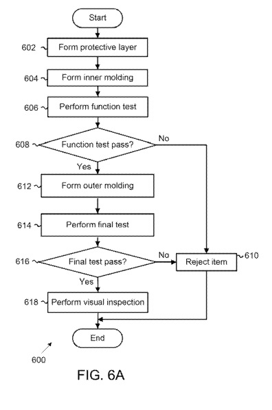
FIG. 6A illustrates an exemplary process for component protective overmolding.
Here, the start
of process 600 includes forming a protective layer on, for example, framework
102 (FIG. 1) (602). In some
examples, a protective layer may refer to protective material, layers, or
covers such as protective material
108 (FIG. 2) or structures that are formed to protect underlying elements
(e.g., covering 108 (FIG. 1).
Examples of material that may be used to form a protective layer include UV
curable materials such as those
described above, including coatings, adhesives, liquids, gels, and others that
cure when exposed to
ultraviolet radiation in various concentrations and exposure levels without
limitation. After forming a
protective layer (e.g., protective coating 208), an inner molding (e.g., inner
molding 312 (FIG. 3)) is formed
(604). After forming an inner molding, a function test is performed to
determine whether the inner molding
and protective layer have damaged the underlying item (606). In some examples,
a function test may be
performed as part of an inspection and include applying an electrical current
to an underlying electronic
element to identify proper voltage or current flow or other parameters that
indicate whether damage has
occurred during the formation of a protective layer, an inner molding, or, in
other examples, an outer
molding. Inspections may be performed at various stages of the manufacturing
process in order to identify
defects early and reduce costs incurred with re-applying protective layers or
moldings. In other examples, a
function test may be performed to determine whether the inner molding has
sufficiently coated desired
underlying items (e.g., electrical, electronic, mechanical, or any structure
or elements thereof that are being
protected from damage using one or more moldings). In still further examples,
the function test may be
performed to determine whether the formation of an inner molding damaged
underlying items that were
previously protected by the formation of protective layer, the latter of which
may be performed outside of a
mold device or cavity (e.g., mold cavity 302 (FIG. 3) or mold cavity 402 (FIG.
4)) at room temperature
and/or atmospheric conditions, including atmospheric or ambient temperatures,
pressures, and humidity
levels, without limitation.
In some examples, a determination is made as to whether a function test is
passed or failed (608).
Here, if an item having a protective layer and an inner molding fails to pass,
the item is rejected and the
process ends (610). Alternatively, if an item (e.g., framework 102 and
elements 106-108 (FIG. 1)) fails to
pass a function test due to the presence of one or more defects, the inner
molding may be removed and re-
applied. In other examples, the underlying item may be rejected (i.e.,
destroyed, recycled, or otherwise
CA 02810717 2013-03-06
WO 2012/171037 PCT/US2012/041964
7
removed from a lot of items that have successfully passed a function test). If
a determination is made that a
function test has passed as part of an inspection, then an outer molding is
formed over the inner molding and
protective layer (612).
In some examples, the protective layer, inner molding, and outer molding may
be selectively,
partially, or completely applied to a given item. As described here, an outer
molding may also be
configured to completely enclose or encase an underlying item in order to
protect the inner molding, the
protective layer, and any elements from damage. Further, outer molding may be
used to form patterns,
designs, or other surface features or contours for usable, functional, or
aesthetic purposes. As shown here,
after an outer molding is formed, a final test is performed to determine
whether defects are present or the
formation of the outer molding met desired parameters (e.g., did the outer
molding fully coat an item, were
any underlying items damaged, and the like) (614). In some examples, a final
test may also be a function
test, as described above. In other examples, a final test may also evaluate an
item coated with an outer
molding for other purposes. If the final test is not passed, then the item may
be rejected and, in some
examples, the outer molding may be removed and re-applied (i.e., re-formed)
(610). In other example, a
failed final test may also result in the item being rejected and destroyed,
recycled, or otherwise handled as
unacceptable. Finally, after a final test is performed a visual inspection may
be performed to determine
whether an item has been covered by the formed outer molding as desired (618).
In other examples, process
600 may be implemented differently in the order, function, configuration, or
other aspects described and is
not limited to the examples shown and described above.
FIG. 6B illustrates an alternative exemplary process for component protective
ovennolding.
Here, process 620 beings be selectively applying protective material (e.g.,
protective coating 208 (FIG. 2))
to one or more elements (e.g., electrical, electronic, mechanical, structural,
or others) (622). In some
examples, selectively applying protective material may include manually using
an applicator (e.g., syringe
202 (FIG. 2) or any other type of instrument, device, tool, or implement used
to apply protective material) to
deposit a layer, covering, coating, or the like over a desired element. In
other examples, selectively
applying may also include the application of protective material to one, some,
all, or none of the elements
present on a given item. In other words, selectively applying protective
material may be perfoinied
uniformly or non-uniformly without limitation. Types of protective materials
may include curable or non-
curable materials such as those described above, including UV-curable coatings
that, when exposed to
ultraviolet radiation, cure. In other examples, other types of coatings may be
used that, when exposed to
artificial or man-made conditions, cure. Still further, other types of
coatings may be used to form a
protective layer (i.e., protective material) over sensitive elements that may
require the combination of two or
more materials, chemicals, or compounds, such as epoxies, polymers,
elastomers, and the like, without
Here, after selectively applying protective material an inner molding is
formed over a
framework, associated elements (i.e., elements coupled to the framework), and
the previously, selectively-
applied protective material (624). As an example of a framework, a "strapband"
or, as used herein, "band"
may refer to a wearable device that is configured for various data capture,
analysis, communication, and
CA 02810717 2013-03-06
WO 2012/171037 PCT/US2012/041964
8
other purposes. In some examples, a band may refer to a wearable personal data
capture device that, when
worn, may be used to record and store various types of data associated with a
given person's motion,
behavior, and physical characteristics (e.g., body temperature, salinity,
blood sugar, heart rate, respiration
rate, movement, and many others, without limitation). In other examples, a
band may be implemented using
hardware, software, and firmware, where application-specific programs may be
downloaded onto a memory
that is included as an element and protected using the described overmolding
processes. A band may be
implemented as described below in connection with FIGs. 7-9.
Referring back to FIG. 6B, an outer molding is formed over the inner molding,
the framework,
its elements, and the protective material (626). After the outer molding is
foiined, an inspection of the outer
molding is performed to determine whether a defect is present (628). As used
herein, an inspection may
refer to any type of process (e.g., automatic, semi-automatic, manual,
robotic, visual, structural,
radiological, electrical, or others) that is used to determine whether a
defect is present. In some examples,
an inspection may include one or more function (i.e., functional) tests to
determine whether a coated (i.e.,
item receiving protective material and protective layers or coatings) has been
damaged during the layering
process. If a defect (e.g., a damaged item or defective molding) is found,
then the outer molding is removed
(632) and formed again over the inner molding, framework, elements, and
protective material (626). If no
defect is found, then the process ends. Examples of materials that may be used
for moldings (e.g., inner
molding, outer molding) in process 620 include plastics, thermoplastics,
thermoplastic elastomers,
polymers, thermoplastic polymer elastomers, epoxies, alloys, metals, or any
other type of organic or
synthetic material, without limitation. In other examples, process 620 may be
implemented differently in
the order, function, configuration, or other aspects provided and is not
limited to the examples shown and
described above.
FIG. 6C illustrates another alternative exemplary process for component
protective overmolding.
Here, an alternative 2-stage process 640 for component protective overmolding
may be performed. First,
selective application of a securing coating over components placed on, for
example, a framework, may be
performed (642). As used herein, a securing coating may refer to any type of
protective material, layer,
cover, structure, liquid, gel, solid, or the like that is placed substantially
(i.e., partially or entirely) over an
item in order to prevent damage from later stages of a manufacturing process
(e.g., introduction into mold
cavity 302 (FIG. 3) or mold cavity 402 (FIG. 4) in which rigorous
temperatures, pressures, or other
environmental conditions are created in order to apply other coated materials.
Further, due to the size and
relatively sensitive operating, manufacturing, and performance characteristics
of various electrical,
electronic, mechanical, or structural features (e.g., microprocessors, solid
state computer memories, control
logic and circuitry, microvibrators, motors, motor controllers, batteries,
battery modules, battery controllers,
and the like), the addition of protective material can prevent inadvertent
damage and increased costs
occurring during the manufacturing of finished products. As an example,
consumer electronics devices
receiving both aesthetic and functional protective overmoldings (i.e.,
moldings) can be expensive to
manufacture because, for each damage underlying electronic component, an
entire unit must be discarded.
However, by using the described techniques to protect sensitive and expensive
elements by replacing
CA 02810717 2013-03-06
WO 2012/171037 PCT/US2012/041964
9
moldings as opposed to entire partially-finished items, manufacturing costs
can be significantly reduced,
thus increasing profit margins and incentives for individuals and enterprises
to commercially invest in
manufacturing devices that can advantageously capture, analyze, use,
communicate (via wired or wireless
data communication facilities (e.g., network interface cards (NICs), wireless
radios using various types of
wireless data communication protocols for short, medium, and long-range
communication (e.g.,
Bluetooth'TM, ZigBee, ANT1m, WiFi, WiMax, and others), and the like), or
otherwise use valuable and
abundant personal data. As an example of these types of devices, a strapband
or band may be a wearable
device that is configured to capture data such as that described above.
Sensitive elements of various sizes
and shapes may be protected from damage occurring during later stages of
protective overmolding (i.e.,
application of protective layers, covers, molds, or the like) using the
described techniques.
Here, after applying a securing coating, another molding may be formed over
the securing
coating, band, and components (e.g., elements) (644). As described here and
above, the application of one
or more moldings may be performed to both secure and protect underlying items
(e.g., components or
elements) of a finished product for various conditions such as use, weather,
shock, temperature, or other
environmental conditions to which finished products (e.g., band) may be
subjected. In other examples,
more, fewer, or different steps may be implemented as part of process 620
including, for example, a single-
stage process involving the application of one or more protective layers
(e.g., housings, coverings, securing
coatings, coatings, moldings, or the like). The functions, operations, or
processes performed during a single
or multi-stage or step process may be varied, without limitation, to include
more, fewer, or different types of
sub-processes apart from those shown and described. Alternatively, more steps
in process 620 may be
implemented are not limited to any of the examples shown and described. In
still other examples, process
620 may be implemented differently in the order, function, configuration, or
other aspects provided and is
not limited to the examples shown and described above.
FIG. 6D illustrates yet another alternative exemplary process for component
protective
overmolding. Here, process 650 begins by placing one or more elements on a
framework (652). In some
examples, the one or more elements may be placed on a part of a framework (not
shown) or other support
structure configured to provide a substrate or base support. Once placed, the
elements are coated using a
curable material (654). As an example of a curable material, Loctitet 5083 UV
curable coating may be
layered (i.e., deposited, poured, injected, layered, or otherwise covered)
over the elements and the
framework. The curable material may be comprehensively, universally,
uniformly, semi-uniformly,
irregularly, or selectively placed so that some elements are covered while
others are left uncovered.
Reasons for selectively applying the curable coating may include other
elements being protected from
damage during the molding process using physical structures (e.g., covering
108) and yet others being
manufactured to withstand the environmental conditions (e.g., temperature
ranges between 400 and 460
degrees Fahrenheit and injection nozzle pressures of 200 to 600 pounds per
square inch (psi)) of molding
cavity 302 (FIG. 3) or 402 (FIG. 4) without using protective material.
After securing elements to a framework using curable material (e.g., UV
curable coating, which
may also be replaced with other types of curable coating, without limitation
or restriction to any specific
CA 02810717 2013-03-06
WO 2012/171037 PCT/US2012/041964
10
type), an inspection may be performed to determine whether there are any
defects, gaps, openings, or other
susceptibilities that can be anticipated before applying the first or inner
molding (656). After performing an
inspection on the curable coating, one or more moldings may be formed over the
curable material (i.e.,
coating), framework, and elements (658) after which an inspection may be
performed to determine whether
there are defects in the molding(s) (660). During the inspection, a
determination is made as to whether a
defect has been found in one or more moldings (662). If a defect is found, the
defective molding is removed
(664) and another molding may be reformed over the curable material,
framework, and elements (666). By
enabling a defective molding to be replaced without requiring the discard of a
framework and its associated
elements (e.g., electrical and electronic components such as microprocessors,
processors, data storage and
computer memory, sensors (e.g., accelerometers, motion/audio/light sensors,
velocimeters, pedometers,
altimeters, heart rate monitors, barometers, chemical/protein detectors, and
others, without limitation),
mechanical and structural features or functionality), substantial costs can be
saved thus enabling devices to
be produced at lower costs to consumers and business alike. In other examples,
process 650 may be
implemented differently in the order, function, configuration, or other
aspects provided and is not limited to
the examples shown and described above.
FIG. 7 illustrates a side view of an exemplary data-capable strapband
configured to receive
overmolding. Here, band 700 includes framework 702, covering 704, flexible
circuit 706, covering 708,
motor 710, coverings 714-724, analog audio plug 726, accessory 728, control
housing 734, control 736, and
flexible circuit 738. In some examples, band 700 is shown with various
elements (i.e., covering 704,
flexible circuit 706, covering 708, motor 710, coverings 714-724, analog audio
plug 726, accessory 728,
control housing 734, control 736, and flexible circuit 738) coupled to
framework 702. Coverings 708, 714-
724 and control housing 734 may be configured to protect various types of
elements, which may be
electrical, electronic, mechanical, structural, or of another type, without
limitation. For example, covering
708 may be used to protect a battery and power management module from
protective material formed
around band 700 during an injection molding operation. As another example,
housing 704 may be used to
protect a printed circuit board assembly ("PCBA") from similar damage.
Further, control housing 734 may
be used to protect various types of user interfaces (e.g., switches, buttons,
lights, light-emitting diodes, or
other control features and functionality) from damage. In other examples, the
elements shown may be
varied in quantity, type, manufacturer, specification, function, structure, or
other aspects in order to provide
data capture, communication, analysis, usage, and other capabilities to band
700, which may be worn by a
user around a wrist, arm, leg, ankle, neck or other protrusion or aperture,
without restriction. Band 700, in
some examples, illustrates an initial unlayered device that may be protected
using the techniques for
protective overmolding as described above.
FIG. 8 illustrates a view of an exemplary data-capable strapband having a
first molding. Here,
band 800 includes molding 802, analog audio plug (hereafter "plug") 804, plug
housing 806, button 808,
framework 810, control housing 812, and indicator light 814. In some examples,
a first protective
overmolding (i.e., molding 802) has been applied over band 700 (FIG. 7) and
the above-described elements
(e.g., covering 704, flexible circuit 706, covering 708, motor 710, coverings
714-724, analog audio plug
CA 02810717 2013-03-06
WO 2012/171037 PCT/US2012/041964
11
726, accessory 728, control housing 734, control 736, and flexible circuit
738) leaving some elements
partially exposed (e.g., plug 804, plug housing 806, button 808, framework
810, control housing 812, and
indicator light 814). However, internal PCBAs, flexible connectors, circuitry,
and other sensitive elements
have been protectively covered with a first or inner molding that can be
configured to further protect band
800 from subsequent moldings formed over band 800 using the above-described
techniques. In other
examples, the type, configuration, location, shape, design, layout, or other
aspects of band 800 may be
varied and are not limited to those shown and described. For example, plug 804
may be removed if a
wireless communication facility is instead attached to framework 810, thus
having a transceiver, logic, and
antenna instead being protected by molding 802. As another example, button 808
may be removed and
replaced by another control mechanism (e.g., an accelerometer that provides
motion data to a processor that,
using firmware and/or an application, can identify and resolve different types
of motion that band 800 is
undergoing), thus enabling molding 802 to be extended more fully, if not
completely, over band 800. In yet
other examples, molding 802 may be shaped or formed differently and is not
intended to be limited to the
specific examples shown and described for purposes of illustration.
FIG. 9 illustrates a view of an exemplary data-capable strapband having a
second molding.
Here, band 900 includes molding 902, plug 904, and button 906. As shown
another overmolding or
protective material has been formed by injection molding, for example, molding
902 over band 900. As
another molding or covering layer, molding 902 may also be configured to
receive surface designs, raised
textures, or patterns, which may be used to add to the commercial appeal of
band 900. In some examples,
band 900 may be illustrative of a finished data capable strapband (i.e., band
700 (FIG. 7), 800 (FIG. 8) or
900) that may be configured to provide a wide range of electrical, electronic,
mechanical, structural,
photonic, or other capabilities.
Here, band 900 may be configured to perform data communication with one or
more other data-
capable devices (e.g., other bands, computers, networked computers, clients,
servers, peers, and the like)
using wired or wireless features. For example, a TRRS-type analog audio plug
may be used (e.g., plug
904), in connection with firmware and software that allow for the transmission
of audio tones to send or
receive encoded data, which may be perfoltned using a variety of encoded
waveforms and protocols,
without limitation. In other examples, plug 904 may be removed and instead
replaced with a wireless
communication facility that is protected by molding 902. If using a wireless
communication facility and
protocol, band 900 may communicate with other data-capable devices such as
cell phones, smart phones,
computers (e.g., desktop, laptop, notebook, tablet, and the like), computing
networks and clouds, and other
types of data-capable devices, without limitation. In still other examples,
band 900 and the elements
described above in connection with FIGs. 1-9, may be varied in type,
configuration, function, structure, or
other aspects, without limitation to any of the examples shown and described.
Although the foregoing examples have been described in some detail for
purposes of clarity of
understanding, the above-described inventive techniques are not limited to the
details provided. There are
many alternative ways of implementing the above-described invention
techniques. The disclosed examples
are illustrative and not restrictive.