Note: Descriptions are shown in the official language in which they were submitted.
CA 02810841 2013-03-21
POWER CIRCUIT
BACKGROUND OF THE INVENTION
The present invention relates to a power circuit that allows a battery to
supply voltage stably to a load in a vehicle with an idling stop control.
Recently a vehicle with an idling stop control has been put to practical
use for reducing fuel consumption and exhaust gas emission. The idling stop
control of the vehicle turns off its engine automatically when it is detected
that the
vehicle stops e.g. at a traffic light and restarts the engine automatically
when it is
detected that the vehicle is about to start again.
When the engine of such vehicle is restarted after an idling stop, a
large current flows to a starter motor of the vehicle, so that the voltage of
a battery
of the vehicle is dropped temporarily. Accordingly, the voltage of power to
various loads such as electronic devices other than the starter motor which
are
connected to the battery is also dropped temporarily at a restart of the
vehicle.
Therefore, there is a fear that the voltage falls below a level that is
required for
any electronic device to operate properly, thus inviting a temporary
malfunction of
the device. For example, a car navigation system and an audio system may be
reset or a sound may jump in the audio system. Thus, unforeseeable operation
of any electronic device may occur.
To solve the above problem, a power circuit may be provided between
the battery and the load so as to keep constant the voltage required for the
loads
even when a voltage drop of the battery occurs temporarily.
Japanese Patent Application Publication 2005-112250 discloses a
power circuit to solve the above problem. The power circuit includes a boost
circuit and a bypass relay that bypasses the boost circuit when the relay is
closed.
At a restart of an engine after an idling stop, the boost circuit is activated
with the
1
CA 02810841 2013-03-21
bypass relay kept opened, so that the voltage of a battery is boosted by the
boost
circuit and the boosted voltage is supplied to various electronic loads of the
vehicle. During a normal state other than the restart of the engine, the
bypass
relay is kept closed thereby to bypass the boost circuit, so that the voltage
of the
battery is supplied to the loads through the bypass relay.
When the voltage of the battery is dropped temporarily at the restart of
the engine after an idling stop, the power circuit ensures that the voltage
required
for the loads is supplied. Meanwhile, during the normal state other than the
restart of the engine, the voltage of the battery is supplied to the loads
without
being dropped by a switching element in the boost circuit, so that supply of
the
voltage required for the loads can be maintained.
However, if an open fault occurs in the bypass relay in the power
circuit and the voltage of the battery is supplied at all times to the loads
through
the boost circuit, the voltage of the battery to be supplied to the loads is
dropped
by the switching element in the boost circuit.
The present invention is directed to providing a power circuit that
allows supply of a stable voltage to loads of electronic devices of a vehicle
equipped with an idling stop control.
SUMMARY OF THE INVENTION
A power circuit includes a boost circuit having a boost switching
element, a coil provided between a battery and the boost switching element and
a
rectifier element provided between the coil and a load, a first switch
connected to
the boost circuit in parallel, a current detection circuit detecting current
flowing
through the first switch and a control circuit turning on the first switch
during a
normal state other than a restart of an engine after an idling stop and
turning off
the first switch and controlling an operation of the boost switching element
at a
restart of the engine after an idling stop so that voltage of the battery is
boosted
2
CA 02810841 2014-07-31
and supplied to the load. The control circuit determines based on the current
detected by the current detection circuit during the normal state whether or
not
the first switch has an open fault.
According to an aspect, the invention provides for a power circuit
comprising: a boost circuit, which includes a boost switching element, a coil
provided between a battery and the boost switching element, and a rectifier
element provided between the coil and a load; a first Metal Oxide
Semiconductor Field Effect Transistor (MOSFET) connected to the boost circuit
in parallel; a current detection circuit detecting current flowing through the
first
MOSFET; and a control circuit turning on the first MOSFET during a normal
state other than a restart of an engine after an idling stop, the control
circuit
turning off the first MOSFET and controlling an operation of the boost
switching
element at a restart of the engine after an idling stop so that voltage of the
battery is boosted and supplied to the load, wherein the control circuit
repeatedly determines at a predetermined time interval based on the current
detected by the current detection circuit during the normal state whether or
not
the first MOSFET has an open fault.
According to another aspect, the invention provides for a power
circuit comprising: a boost circuit which includes a boost switching element,
a
coil provided between a battery and the boost switching element, and a
rectifier
element provided between the coil and a load; a first Metal Oxide
Semiconductor Field Effect Transistor (MOSFET) connected to the boost circuit
in parallel; a potential difference output circuit detecting potential
difference
between input voltage and output voltage of the boost circuit; and a control
circuit turning on the first MOSFET during a normal state other than a restart
of
an engine after an idling stop, the control circuit turning off the first
MOSFET
and controlling an operation of the boost switching element at a restart of
the
engine after an idling stop so that voltage of the battery is boosted and
supplied
to the load, wherein the control circuit determines based on the potential
difference detected by the potential difference output circuit during the
normal
state whether or not the first MOSFET has an open fault.
3
CA 02810841 2014-07-31
Other aspects and advantages of the invention will become apparent
from the following description, taken in conjunction with the accompanying
drawings, illustrating by way of example the principles of the invention.
BRIEF DESCRIPTION OF THE DRAWINGS
The features of the present invention that are believed to be novel are
set forth with particularity in the appended claims. The invention together
with
objects and advantages thereof, may best be understood by reference to the
following description of the presently preferred embodiments together with the
accompanying drawings in which:
FIG. 1 is a schematic configuration diagram showing a power circuit
according to a first embodiment of the present invention;
FIG. 2 is a flowchart showing the operation of the power circuit of FIG.
1;
FIG. 3 is a schematic configuration diagram showing a power circuit
according to a second embodiment of the present invention;
FIG. 4 is a schematic configuration diagram showing a power circuit
according to a third embodiment of the present invention;
FIG. 5 is a schematic configuration diagram showing a power circuit
according to a fourth embodiment of the present invention;
FIG. 6 is a schematic configuration diagram showing a power circuit
according to a fifth embodiment of the present invention;
FIG. 7 is a schematic configuration diagram showing a power circuit
according to a sixth embodiment of the present invention; and
FIG. 8 is a schematic configuration diagram showing a power circuit
according to a seventh embodiment of the present invention.
DETAILED DESCRIPTION OF THE PREFERRED EMBODIMENTS
3a
CA 02810841 2013-03-21
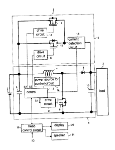
Referring to FIG. 1, the power circuit according to the first embodiment
of the present invention is generally designated by numeral 1. The power
circuit
1 is adapted to keep constant the voltage of a battery 2 which is mounted on a
no-idling vehicle and also to supply the voltage to a load 3. The power
circuit 1
includes a boost circuit 4 and a bypass circuit 5.
The boost circuit 4 boosts the voltage of the battery 2 and supplies the
boosted voltage to the load 3 at a restart of an engine after an idling stop
of the
engine. The boost circuit 4 includes a boost switching element 6, a coil 7, a
rectifier diode 8 (or a rectifier element), capacitors 9, 10, a drive circuit
11, a
control circuit 13 and a power source 12 for the control circuit 13.
The boost switching element 6 is e.g. of Metal Oxide Semiconductor
Field Effect Transistor (MOSFET) or Insulated Gate Bipolar Transistor (IGBT).
The coil 7 is provided between the battery 2 and the boost switching
element 6. The rectifier diode 8 is provided between the coil 7 and the load
3.
The capacitor 9 is provided in the input stage of the boost circuit 4.
The capacitor 10 is provided in the output stage of the boost circuit 4.
The drive circuit 11 drives the boost switching element 6 based on a control
signal
S1 transmitted by the control circuit 13.
The power source 12 supplies power to the control circuit 13. The
bypass circuit 5 includes a first switch 14, a second switch 15, drive
circuits 16, 17
and a current detection circuit 18.
The first and the second switches 14, 15 are e.g. of a MOSFET or a
relay and connected to the boost circuit 4 in parallel. The drive circuit 16
drives
the first switch 14 based on a control signal S2 transmitted by the control
circuit
13 and the drive circuit 17 drives the second switch 15 based on a control
signal
4
CA 02810841 2013-03-21
S3 transmitted by the control circuit 13.
The current detection circuit 18 is made e.g. of a shunt resistance, a
current transformer or a Hall element and serves as a current detection
sensor.
The current detection circuit 18 is provided between the connecting point of
the
first and the second switches 14, 15 and the load 3.
The control circuit 13 transmits control signals Si through S3 based
on various data sent by a head control circuit 19. The control circuit 13
consists
of software or hardware. The control circuit 13 consisting of software
includes a
CPU and a memory. A program stored in the memory is read and executed by
the CPU. The control circuit 13 may be provided outside the boost circuit 4.
During the normal state other than the restart of the engine
subsequent to an idling stop, the control circuit 13 transmits control signals
S2,
S3 for keeping the first and the second switches 14, 15 on or closed based on
various data sent from the head control circuit 19 and also a control signal
Si for
keeping the boost switching element 6 off or opened. During such normal state,
the battery 2 is electrically connected to the load 3 through the then closed
first
and second switches 14, 15, so that electric current flows from the battery 2
to the
load 3 through the switches 14, 15, bypassing the boost circuit 4. Therefore,
no
boosting of the voltage of the battery 2 is performed by the boost circuit 4.
Supplying of the required voltage to the load 3 during the normal state other
than
restarting of the engine subsequent to an idling stop can be maintained by
making the voltage drop of the battery 2 due to the first and the second
switches
14, 15 of the bypass circuit 5 smaller than that due to the coil 7 and the
rectifier
diode 8 of the boost circuit 4. This mode of operation of the control circuit
13 will
be hereinafter referred to as "bypass mode".
At a restart of the engine after an idling stop, the control circuit 13
transmits the control signals S2, S3 as well as Si, wherein the signals S2, S3
are
used for keeping the first and the second switches 14, 15 off or opened and
the
5
CA 02810841 2013-03-21
signal Si for causing the boost switching element 6 to repeat on and off
operation.
Thus, the electrical connection between the battery 2 and the load 3 through
the
first and the second switches 14, 15 is cut off, but the boost circuit 4 is
activated to
boost the voltage of the battery 2, so that the boosted voltage of the battery
2 is
supplied to the load 3. Therefore, even if the voltage of the battery 2 is
dropped
temporarily due to the operation of the starter motor for restarting of the
engine,
supplying of the voltage required for the load 3 can be maintained. This mode
of
operation of the control circuit 13 will be hereinafter referred to as "boost
mode".
In the bypass mode operation, the control circuit 13 determines
whether or not the current detected by the current detection circuit 18 at a
predetermined time interval (e.g. 5 seconds) is at a threshold value Rh (e.g.
5A
(amperes)) or higher. If the control circuit 13 determines that the detected
current is less than Ith, in other words, when the load 3 is not driven and no
current (e.g. 5A) is flowed to the load 3, the bypass mode is continued. On
the
other hand, if the control circuit 13 determines that the detected current is
at lth or
more, in other words, when the load 3 is being driven and a current is flowed
to
the load 3, it will be determined whether or not either or both of the first
and the
second switches 14, 15 suffers from open fault.
In the bypass mode of operation, the control circuit 13 determines
whether or not the first and the second switches 14, 15 have an open fault in
the
following manner. The control circuit 13 transmits the control signals S2, S3
to
keep the first switch 14 on or closed and keep the second switch 15 off or
opened
for a predetermined length of time (e.g. 5 mS), respectively. If the current
detected by the current detection circuit 18 is 0 A or substantially 0 A, the
control
circuit 13 determines that first switch 14 has an open fault and informs the
head
control circuit 19 (or output means) of the result. Subsequently, the head
control
circuit 19 gives the warning that the first switch 14 has an open fault on a
display
20 (or output means) or by a speaker 20 (or output means).
The control circuit 13 also transmits the control signals S2, S3 to keep
6
CA 02810841 2013-03-21
the first switch 14 off or opened and keep the second switch 15 on or closed
for a
predetermined length of time (e.g. 5 mS), respectively. If the current
detected by
the current detection circuit 18 is 0 A or substantially 0 A, the control
circuit 13
determines that the second switch 15 has an open fault and informs the head
control circuit 19 (or output means) of the result. The head control circuit
19
gives the warning that the second switch 15 has an open fault on the display
20
or by the speaker 21. Thus, during the normal state, the control circuit 13
turns
off the first switch 14 and the second switch 15 alternately at a regular time
interval (e.g. 5 S) and determines based on the current detected by the
current
detection circuit 18 whether or not the first switch 14 has an open fault
while the
second switch 15 is turned off and also whether or not the second switch 15
has
an open fault while the first switch 14 is turned off.
FIG. 2 is the flowchart showing the operation of the control circuit 13 of
FIG. 1. It is assumed that the first and the second switches 14, 15 are both
turned on or closed in the initial state (e.g. in a parked state before
starting the
engine).
If the control circuit 13 is informed by the head control circuit 19 that
an ignition signal (IG) is turned to a high level by user's (e.g. driver's)
manipulation of the ignition switch (if Yes at S21), the boost mode operation
will
be executed until a predetermined length of time has elapsed (S22¨S24). It is
assumed that the starter motor is started to drive the engine of the vehicle
when
the ignition signal is turned to a high level and also that the predetermined
length
of time is substantially the same as the length of time of the voltage drop of
the
battery 2 due to the operation of the starter motor.
The control circuit 13 reads the current detected by the current
detection circuit 18 and sets the read current as the offset value (S25). In
other
words, the control circuit 13 sets the value of the current detected by the
current
detection circuit 18 as the offset value during the time after the end of the
boost
mode operation and also before the start of the bypass mode operation (or the
7
CA 02810841 2013-03-21
time when the first and the second switches 14, 15 are both kept off or opened
and also the boost switching element 6 is kept off or opened).
After a start of the bypass mode operation (S26), if the control circuit
13 is informed by the head control circuit 19 of a restart of the engine after
an
idling stop (if Yes at S27), the process returns to 822.
On the other hand, if the control circuit 13 is not informed by the head
control circuit 19 of a restart of the engine after an idling stop (if No at
S27) and
also the predetermined length of time (5 seconds) has elapsed (if Yes at S28)
after the start of the bypass mode (S26), the control circuit 13 reads the
current
detected by the current detection circuit 18 (S29) and determines whether or
not
the value of the current is at the threshold value Ith or more (S30).
If the control circuit 13 determines that the value of the current that is
read at S29 is less than the threshold value lzh (if No at S30) and
subsequently
the control circuit 13 is informed by the head control circuit 19 of a restart
of the
engine after an idling stop (if Yes at S31), the control circuit 13 finishes
the bypass
mode operation (S32) and returns the process to S22.
On the other hand, if the control circuit 13 determines that the value of
the current read at S29 is less than the threshold value lzh (if No at S30)
and
subsequently the control circuit 13 receives no information from the head
control
circuit 19 of a restart of the engine after an idling stop (if No at S31), the
control
circuit 13 reads again the current detected by the current detection circuit
18
(S29) after an elapse of the predetermined length of time (Yes at S28) and
determines whether or not the value of the current is at the threshold value
Ith or
more (S30).
[0039]
When the control circuit 13 determines that the value of the current
read at 829 is at the threshold value lzh or more (if Yes at S30), the control
circuit
13 turns on the first switch 14 and turns off the second switch 15 (S33).
8
CA 02810841 2013-03-21
Subsequently, the control circuit 13 reads the current detected by the current
detection circuit 18 (S34) and corrects the current by the offset value that
has
been set at S25 and determines whether or not the corrected current is 0 A or
substantially 0 A (S35). Specifically, the control circuit 13 sets the value
that is
figured out by subtracting the offset value set at S25 from the value of the
current
detected at S34 as the corrected current value at S35.
If the control circuit 13 determines that the corrected current value is 0
A or substantially 0 A (if Yes at S35), the control circuit 13 informs the
head control
circuit 19 that the first switch 14 has an open fault (S36) and the process
goes to
S37.
On the other hand, when the control circuit 13 determines that the
corrected current value is neither 0 A nor substantially 0 A (S35 is No), the
control
circuit 13 turns off the first switch 14 and turns on the second switch 15
(S17).
Subsequently, the control circuit 13 reads the current detected by the current
detection circuit 18 (S38) and corrects the current by the offset value set at
S25
and determines whether or not the corrected current value is 0 A or
substantially 0
A (839). Specifically, the control circuit 13 sets the value that is figured
out by
subtracting the offset value set at S25 from the value of the current detected
at
S38 as the corrected current value at S39.
If the control circuit 13 determines that the corrected current value is 0
A or substantially 0 A (if Yes at S39), the control circuit 13 informs the
head control
circuit 19 that the second switch 15 has an open fault (S40) and the process
goes
to S41.
On the other hand, if the control circuit 13 determines that the
corrected current value is neither 0 A nor substantially 0 A (S39 is No), the
control
circuit 13 turns on the first and the second switches 14, 15 and determines
whether or not the control circuit 13 per se is informed by the head control
circuit
19 of a restart of the engine after an idling stop (S31).
9
CA 02810841 2013-03-21
According to the power circuit 1 of the first embodiment having the first
and the second switches 14, 15, even if either one of the first and the second
switches becomes unserviceable due to an open fault, the voltage of the
battery 2
can be maintained and supplied to the load 3 of the vehicle through the other
usable switch during the normal state other than a restart of the engine after
an
idling stop. Thus, the voltage of the battery 2 can be supplied stably to the
load
3 of a vehicle with an idling stop control. Additionally, the provision of the
two
switches 14, 15 in the bypass circuit 5 permits the battery 2 to supply its
voltage to
the load 3 through one of the switches 14, 15 even if the other of the
switches 14,
is faulty. As a result, no current flows from the battery 2 to the boost
circuit 4
during the bypass mode operation and, therefore, heat generation of the coil 7
or
the rectifier diode 8 is prevented, with the result that the coil 7 or the
rectifier diode
8 can be protected against damage due to such heat.
The electronic devices that are related to fundamental performances
of a vehicle such as traveling, turning and stopping and, therefore, need be
supplied with a strictly controlled voltage can be used as the load 3
connected to
the power circuit 1 that supplies power stably. Additionally, the power
circuit 1 is
configured so that no current flows from the battery 2 to the load 3 through
the
boost circuit 4 during the normal state operation of the engine. Therefore,
the
boost circuit 4 of the power circuit 1 need not use a large-capacity element
for the
coil 7 and the rectifier diode 8, which helps to decrease the cost of the
power
circuit 1.
The power circuit 1 according to the first embodiment which
determines whether or not either or both of the first and the second switches
14,
15 has an open fault and informs the vehicle user of the state of the switches
14,
15 by the display 20 or the speaker 21 allows the user to recognize any
trouble of
the first switch 14 or the second switch 15. Therefore, the user can be
prompted
to replace the faulty switch or a unit including the faulty switch with a new
one so
as to restore the power circuit 1 timely.
CA 02810841 2013-03-21
The power circuit 1 shown in FIG. 1 has only one current detection
circuit 18, but may have two or more current detection circuits 18. For
example,
the power circuit 1 according to the second embodiment includes two current
detection circuits, as shown in FIG. 3. The bypass circuit 5 of the power
circuit 1
has a current detection circuit 31 for detecting the current flowing through
the first
switch 14 and a current detection circuit 32 for detecting the current flowing
through the second switch 15. In the control circuit 13 shown in FIG. 3,
during
the time after the boost mode operation and also before the bypass mode
operation (or when the first and the second switches 14, 15 are both turned
off
and the boost switching element 6 is also turned off), the values of the
currents
then flowing through the first and the second switches 14, 15 are set as the
offset
values A and B, respectively. In the control circuit 13 shown in FIG. 3, if
the sum
of the values of the currents detected by the current detection circuits 31,
32 is at
the threshold value Ith or more during the bypass mode operation and it is
determined that at least one of the values of the currents read by the current
detection circuits 31, 32 is 0 A or substantially 0 A, the head control
circuit 19 is
informed that the switch corresponding to the current detection circuit that
shows
0 A or substantially 0 A has an open fault. According to the second
embodiment,
in determining the open fault of the first switch 14 or the second switch 15,
the
first and the second switches 14, 15 need not be turned off alternately and
also
the currents need not be read many times, so that the operation of the control
circuit 13 can be simplified. Additionally, the current detection circuits are
redundant in the power circuit 1 shown in FIG. 3, so that the accuracy of
determining the open fault of the first switch 14 or the second switch 15 can
be
improved.
The power circuit 1 shown in FIG 1 or 3 is configured so that the open
fault of the first switch 14 or the second switch 15 is determined based on
the
current detected by the current detection circuits 18, 31, 32. The power
circuit 1
according to the third embodiment shown in FIG. 4 differs from the power
circuits
1 of the first and the second embodiments in that a potential difference
detection
11
CA 02810841 2013-03-21
circuit 41 is provided which detects the potential difference between the
input and
the output voltages of the boost circuit 4 and transmits a signal that is
indicative of
the detected potential difference to the control circuit 13 which determines
whether or not an open fault is present in any of the first switch 14 and the
second
switch 15 based on the detection signal from the potential difference
detection
circuit 41. If either one of the first and the second switches 14, 15 has an
open
default when one of the switches 14, 15 is turned on and the other of the
switches
14, 15 is turned off, the current flows from the battery 2 to the load 3
through the
boost circuit 4 without flowing through the bypass circuit 5. The voltage drop
of
the battery 2 due to the coil 7 and the rectifier diode 8 in the boost circuit
4 is
greater than that due to the first and the second switches 14, 15 in the
bypass
circuit 5. Therefore, the potential difference detected by the potential
difference
detection circuit 41 when the current flows from the battery 2 to the load 3
through
the boost circuit 4 is greater than in the case when the current flows from
the
battery 2 to the load 3 through the bypass circuit 5. During the bypass mode
operation, if the potential difference outputted by the potential difference
detection
circuit 41 is at the threshold value Vth or greater when one of the first and
the
second switches 14, 15 is turned on and the other of the switches 14, 15 is
turned
off, the control circuit 13 of FIG. 4 determines that one of the first and the
second
switches 14, 15 has an open fault and informs the head control circuit 19 of
the
result. The threshold value Vth may be or substantially the same as the
potential difference outputted by the potential difference detection circuit
41 when
a current flows from the battery 2 to the load 3 through the bypass circuit 5
at the
bypass mode.
In the power circuit 1 shown in FIG. 1, 3 or 4, the rectifier diode 8
serves as the rectifier element in the 'respective boost circuits 4. The power
circuit 1 according to the fourth embodiment shown in FIG. 5 differs from the
foregoing embodiments of FIGS. 1, 3 and 4 in that a rectifier switching
element 51
(e.g. IGBT having MOSFET and diode connected in parallel) is used to serve as
the rectifier element in the boost circuit 4. A drive circuit 52 is provided
in the
boost circuit 4 to drive the rectifier switching element 51 based on the
control
12
CA 02810841 2013-03-21
4
signal 84 transmitted by the control circuit 13. The control circuit 13 shown
in
FIG. 5 turns on and off the boost switching element 6 and the rectifier
switching
element 51 alternately during the boost mode operation. The power circuit 1 of
this embodiment can reduce the energy loss due to the rectifier element as
5 compared with a case wherein the rectifier diode 8 serves as the
rectifier element
in the boost circuit 4.
The power circuit 1 shown in FIG. 1, 3, 4 or 5 is so configured that the
first and the second switches 14, 15 in the bypass circuit 5 are connected to
the
boost circuit 4 in parallel. However, the bypass circuit 5 may have more than
two switches connected to the boost circuit 4 in parallel. For example, the
power
circuit 1 according to the fifth embodiment shown in FIG. 6 has three switches
14,
and 61 which are connected in parallel to the boost circuit 4. As shown FIG.
6,
a drive circuit 62 is provided in the bypass circuit 5 to drive the switch 61
based
15 on the control signal S5 transmitted by the control circuit 13. During
the bypass
mode operation, if the current detected by the current detection circuit 18 is
0 A or
substantially 0 A when the control circuit 13 turns off the first and the
second
switches 14, 15 and turns on the switch 61, it is determined that the switch
61 has
an open fault and the head control circuit 19 (or output means) is informed by
the
control circuit 13 that the switch 61 has an open fault. When the head control
circuit 19 is so informed, the head control circuit 19 gives a message
informing
that the switch 61 has an open fault on the display 20 (or output means) or by
the
speaker 21 (or output means). Thus increasing the number of switches in the
bypass circuit 5, the probability of a state wherein all the switches in the
bypass
circuit 5 are disabled can be reduced, so that the stability of supplying the
voltage
of the battery 2 to the load 3 can be improved.
The power circuit 1 shown in FIG. 1, 3, 4 or 5 is so configured that
each of the first and the second switches 14, 15 is connected to the boost
circuit 4
in parallel. However, the power circuit 1 may be configured so that only one
switch in the bypass circuit 5 is connected to the boost circuit 4 in
parallel. Such
examples are shown in FIGS. 7 and 8 illustrating the power circuit 1 according
to
13
CA 02810841 2013-03-21
the sixth and the seventh embodiments, wherein only one switch designated by
14 is connected to the boost circuit 4 in parallel, respectively.
30
14