Note: Descriptions are shown in the official language in which they were submitted.
CA 02811457 2013-03-15
WO 2012/058757 PCT/CA2011/001217
PHASE DETECTOR
TECHNICAL FIELD
[0001] The present disclosure is directed at a phase detector that
generates a metric that is
a function of a phase difference between a modulated carrier and a local
carrier.
BACKGROUND
[0002] Wireless digital communications often involves transmission of
symbols using a
modulated carrier and the subsequent coherent demodulation of the modulated
carrier by a
receiver. One way to perform coherent demodulation is to synchronize the
receiver's local
carrier with the modulated carrier using a phase locked loop (PLL). PLLs
attempt to eliminate
the phase error between the modulated carrier and the local carrier. One
component of a PLL is
a phase detector.
[0003] In digital communications, and particularly in mobile digital
communications, it is
beneficial to employ circuitry that is fast, inexpensive, relatively simple,
and power efficient.
Accordingly, research and development continue into improving the designs of
PLLs.
SUMMARY
[0004] According to one aspect, there is provided a method for
generating a metric that is
a function of a phase difference between a modulated carrier and a local
carrier. The method
includes obtaining a baseband symbol from the modulated carrier that is
modulated using the
symbol according to a modulation whose constellation diagram has M-fold
rotational symmetry,
wherein M is a positive integer greater than or equal to 2; determining a
received phase of the
symbol; and generating the metric from the received phase, wherein possible
metrics depend on
possible received phases according to a base function that comprises a
triangle wave having
positively and negatively sloped linear segments whose slopes have identical
absolute values and
that is periodic with a period of 2n/M radians.
[0005] According to another aspect, there is provided a method for
generating a metric
that is a function of a phase difference between a modulated carrier and a
local carrier. The
method includes obtaining a baseband symbol from the modulated carrier that is
modulated
-1-
CA 02811457 2016-09-30
using the symbol according to a modulation order (M) equaling the number of
distinct ideal
symbol phases used to modulate the modulated carrier, wherein ideal symbol
phases are
uniformly distributed within any continuous phase interval spanning 27c
radians; determining the
phase of the symbol; and generating the metric from the phase, wherein
possible metrics depend
on possible phases according to a base function that comprises a triangle wave
having positively
and negatively sloped linear segments whose slopes have identical absolute
values and that is
periodic with a period of 27c/M radians, wherein the ideal symbol phases
correspond to
identically valued metrics located on the triangle wave.
[0006] The maxima and minima of the triangle wave may have identical
absolute values.
[0007] The base function may have a value of zero at each of the ideal
symbol phases.
[0008] The ideal symbol phases may correspond to identical values for
the metric located
along either the positively sloped linear segments or the negatively sloped
linear segments.
[0009] The modulated carrier may be modulated according to QAM and,
optionally,
Rectangular QAM.
[0010] The number of modulation symbols may equal 2k, wherein k is a
positive integer.
[0011] The modulated carrier may be modulated according to M-ary
phase shift keying.
Optionally, M may equal 2k, wherein k is a positive integer.
[0012] The modulation may be selected from the group consisting of
BPSK, QPSK, 8-
PSK, 16-PSK, Rectangular QAM-4, Rectangular QAM-16, Rectangular QAM-64,
Rectangular
QAM-256, Rectangular Offset-QAM-16, Rectangular Offset-QAM-64, Rectangular
Offset-
QAM-256, Offset-QPSK, Offset-8PSK, Offset-16PSK, and Minimum Shift Keying.
[0013] The received phase may be expressed as being between [-n,n)
radians prior to
generating the metric, and the base function may be implemented such that it
spans only [-n,n)
radians.
[0014] The received phase may be encoded using an encoding scheme that
linearly
encompasses substantially all of the possible received phases.
-2-
CA 02811457 2016-09-30
[0015] The metric may be generated as a function of a principal angle
that is directly
proportional to the received phase modulo (762M).
[0016] The principal angle may be normalized such that its supremum
equals the
absolute value of the maxima of the triangle wave.
[0017] The principal angle may include one or more of the least significant
bits of the
received phase.
[0018] Generating the metric may involve inverting the principal
angle as a function of
one or more bits of the received phase; and adding one of A, -A or 0 to the
principal angle or its
inverse as a function of two or more bits of the received phase, wherein A is
the absolute value
of the maxima of the triangle wave.
[0019] The encoding scheme may be one's complement, two's complement,
or sign-
magnitude encoding, the received phase may have b bits, and M may equal 2k,
wherein k is a
positive integer.
[0020] The principal angle may include a plurality of the most
significant bits of bits [b-
3-log2M:0] of the received phase.
[0021] The principal angle may be proportional to a binary number
that includes a
plurality of the most significant bits of bits [b-3-log2M:0] of the received
phase.
[0022] Generating the metric may include inverting the principal
angle as a function of
one or more of the bits [b-1 -log2M:b-2-log2M] of the received phase; and
adding either A, -A or
0 to the principal angle or its inverse as a function of bits [b-1-log2M:b-2-
log2M] of the received
phase, wherein A is the absolute value of the maxima of the triangle wave.
[0023] According to another aspect, there is provided a phase
detector for generating a
metric that is a function of a phase difference between a modulated carrier
and a local carrier.
The phase detector includes a front end configured to obtain a baseband symbol
from the
modulated carrier that is modulated using the symbol according to a modulation
whose
constellation diagram has M-fold rotational symmetry, wherein M is a positive
integer greater
than or equal to 2; a phase determiner communicatively coupled to the front
end and configured
-3-
CA 02811457 2016-09-30
to determine a received phase of the baseband symbol; and a metric generator
communicatively
coupled to the phase determiner and configured to generate the metric from the
received phase,
wherein possible metrics depend on possible received phases according to a
base function that
comprises a triangle wave having positively and negatively sloped linear
segments whose slopes
have identical absolute values and that is periodic with a period of 27E/M
radians.
[0024] According to another aspect, there is provided a phase
detector for generating a
metric that is a function of a phase difference between a modulated carrier
and a local carrier.
The phase detector includes a front end configured to obtain a baseband symbol
from the
modulated carrier that is modulated using the symbol according to a modulation
order (M)
equaling the number of distinct ideal symbol phases used to modulate the
modulated carrier,
wherein ideal symbol phases are uniformly distributed within any continuous
phase interval
spanning 27E radians; a phase determiner communicatively coupled to the front
end and
configured to determine the phase of the baseband symbols; and a metric
generator
communicatively coupled to the phase determiner and configured to determine
the metric from
the phase, wherein possible metrics depend on possible phases according to a
base function that
comprises a triangle wave having positively and negatively sloped linear
segments whose slopes
have identical absolute values and that is periodic with a period of 27E/M
radians, wherein the
ideal symbol phases correspond to identically valued metrics located on the
triangle wave.
[0025] The maxima and minima of the triangle wave may have identical
absolute values
[0026] The base function may have a value of zero at each of the ideal
symbol phases.
[0027] The ideal symbol phases may correspond to identical values for
the metric located
along either the positively sloped linear segments or the negatively sloped
linear segments.
[0028] The modulated carrier may be modulated according to QAM and,
optionally,
Rectangular QAM.
[0029] The number of modulation symbols may equal 2k, wherein k is a
positive integer.
[0030] The modulated carrier may be modulated according to M-ary
phase shift keying
and, optionally, M may equal 2k, wherein k is a positive integer.
-4-
CA 02811457 2016-09-30
[0031] The modulation may be selected from the group consisting of
BPSK, QPSK, 8-
PSK, 16-PSK, Rectangular QAM-4, Rectangular QAM-16, Rectangular QAM-64,
Rectangular
QAM-256, Rectangular Offset-QAM-16, Rectangular Offset-QAM-64, Rectangular
Offset-
QAM-256, Offset-QPSK, Offset-8PSK, Offset-16PSK, and Minimum Shift Keying.
[0032] The phase determiner may be configured to express the received phase
as being
between [-n,n) radians, and the base function may be implemented such that it
spans only [-TEJO
radians.
[0033] The phase determiner may be configured to encode the received
phase using an
encoding scheme that linearly encompasses substantially all of the possible
received phases.
[0034] The metric generator may be configured to determine for the received
phase a
principal angle that is directly proportional to the received phase modulo
(762M) and to
determine the metric as a function of the principal angle.
[0035] The metric generator may be configured to normalize the
principal angle such that
its supremum equals the absolute value of the maxima of the triangle wave.
[0036] The phase determiner may encode the received phase such that the
principal angle
comprises one or more of the least significant bits of the phase.
[0037] The phase determiner may encode the received phase such that
one or more bits
(inversion control bits) of the received phase indicate whether to invert the
principal angle and
such that two or more bits (selection bits) of the received phase indicate
whether to add A, -A or
0 to the principal angle or its inverse, wherein A is the absolute value of
the maxima of the
triangle wave, and the metric generator may include inverting hardware having
(i) a data input to
which the principal angle is input; (ii) an inversion control input to which
the inversion control
bits are input; and (iii) a data output that outputs the inverse of the
principal angle when the
inversion control bits indicate the principal angle is to be inverted and
otherwise outputs the
principal angle; data selection hardware having (i) data inputs to which A, -A
or 0 is input; (ii) a
data selection input to which the selection bits are input; and (iii) a data
output that outputs either
A, -A or 0 in accordance with which one of the data inputs of the data
selection hardware is
selected by the selection bits; and adding hardware having (i) data inputs
communicatively
-5-
CA 02811457 2016-09-30
coupled to the data outputs of the inverting hardware and the data selection
hardware; and (ii) a
data output that outputs the sum of signals at the data inputs of the adding
hardware.
[0038] The inverting hardware may include a first XOR gate configured
to receive the
inversion control bits and an array of XOR gates each having one input to
receive one bit of the
-- principal angle, wherein the output of the first XOR gate is
communicatively coupled to another
input of each of the XOR gates in the array. The data selection hardware may
include a
multiplexer. The adding hardware may include an adder.
[0039] A may be 1.
[0040] The phase determiner may encode the received phase such that a
principal angle
-- precursor includes one or more of the least significant bits of the
received phase, and the
principal angle may be directly proportional to the principal angle precursor.
[0041] The phase determiner may encode the received phase such that
one or more bits
(inversion control bits) of the received phase indicate whether to invert the
principal angle
precursor and such that two or more bits (selection bits) of the received
phase indicate whether to
-- add A, -A or 0 to the principal angle or its inverse, wherein A is the
absolute value of the
maxima of the triangle wave, and the metric generator may include inverting
hardware
comprising (i) a data input to which the principal angle precursor is input;
(ii) an inversion
control input to which the inversion control bits are input; and (iii) a data
output that outputs the
inverse of the principal angle precursor when the inversion control bits
indicate the principal
-- angle precursor is to be inverted and otherwise outputs the principal angle
precursor; data
selection hardware having (i) a data input to which A, -A and 0 are input;
(ii) a data selection
input to which the selection bits are input; and (iii) a data output that
outputs either A, -A or 0 in
accordance with which one of the data inputs of the data selection hardware is
selected by the
selection bits; amplification hardware having (i) a data input communicatively
coupled to the
-- data output of the inverting hardware; and (ii) a data output that outputs
the amplification of the
signal at the data input; and adding hardware having (i) data inputs
communicatively coupled to
the data outputs of the amplification hardware and the data selection
hardware; and (ii) a data
output that outputs the sum of signals at the data inputs of the adding
hardware.
-6-
CA 02811457 2016-09-30
[0042] The phase determiner may encode the received phase in one's
complement, two's
complement, or sign-magnitude encoding. The received phase may have b bits and
M may equal
2k wherein k is a positive integer, and the principal angle may include a
plurality of the most
significant bits of bits [b-3-log2M:0] of the received phase.
[0043] The phase determiner may encode the received phase such that one or
more of
bits [b-1 -log2M:b-2-log2M] (inversion control bits) of the received phase
indicate whether to
invert the principal angle and such that bits [b-log2M-1:b-log2M-2] (selection
bits) of the
received phase indicate whether to add A, -A or 0 to the principal angle or
its inverse, wherein A
is the absolute value of the maxima of the triangle wave, and the metric
generator may include
inverting hardware having (i) a data input to which the principal angle is
input; (ii) an inversion
control input to which the inversion control bits are input; (iii) a data
output that outputs the
inverse of the principal angle when the inversion control bits indicate the
principal angle is to be
inverted and otherwise outputs the principal angle; data selection hardware
having (i) data inputs
to which A, -A or 0 are input; (ii) a data selection input to which the
selection bits are input; and
(iii) a data output that outputs either A, -A or 0 in accordance with which
one of the data inputs
of the data selection hardware is selected by the selection bits; and adding
hardware having (i)
data inputs communicatively coupled to the data outputs of the inverting
hardware and the data
selection hardware; and (ii) a data output that outputs the sum of the data
outputs of the inverting
hardware and the data selection hardware.
[0044] The inverting hardware may be a first XOR gate configured to receive
the
inversion control bits and an array of XOR gates each having one input to
receive one bit of the
principal angle, wherein the output of the first XOR gate is communicatively
coupled to another
input of each of the XOR gates in the array. The data selection hardware may
be a multiplexer.
The adding hardware may be an adder.
[0045] A may be 1.
[0046] The phase determiner may encode the received phase in one's
complement, two's
complement, or sign-magnitude encoding, wherein the received phase may have b
bits and M
may equal 2k wherein k is a positive integer. The principal angle may be
proportional to a
-7-
CA 02811457 2016-09-30
principal angle precursor that includes a plurality of the most significant
bits of bits [b-3-
log2M:0] of the received phase.
[0047]
The phase determiner may encode the received phase such that one or more
of the
bits [b- 1 -log2M:b-2-log2M] (inversion control bits) of the received phase
indicates whether to
invert the principal angle precursor and such that bits [b-log2M-1:b-log2M-2]
(selection bits) of
the received phase indicate whether to add A, -A or 0 to the principal angle
or its inverse,
wherein A is the absolute value of the maxima of the triangle wave, and the
metric generator
may include inverting hardware having (i) a data input to which the principal
angle precursor is
input; (ii) an inversion control input to which the inversion control bits are
input; and (iii) a data
output that outputs the inverse of the principal angle precursor when the
inversion control bits
indicate the principal angle precursor is to be inverted and otherwise outputs
the principal angle
precursor; data selection hardware having (i) a data input to which A, -A and
0 are input; (ii)a
data selection input to which the selection bits are input; and (iii) a data
output that outputs
either A, -A or 0 in accordance with which one of the data inputs of the data
selection hardware
is selected by the selection bits; amplification hardware having (i) a data
input communicatively
coupled to the data output of the inverting hardware; and (ii) a data output
that outputs the
amplification of the signal at the data input; and (d) adding hardware having
(i) data inputs
communicatively coupled to the data outputs of the amplification hardware and
the data selection
hardware; and (ii) a data output that outputs the sum of signals at the data
inputs of the adding
hardware.
[0048]
The inverting hardware may include a first XOR gate configured to receive
the
inversion control bits and an array of XOR gates each having one input to
receive one bit of the
principal angle precursor, wherein the output of the first XOR gate is
communicatively coupled
to another input of each of the XOR gates in the array. The data selection
hardware may include
a multiplexer. The amplification hardware may include a bit shifter. The
adding hardware may
include an adder.
[0049] According to another aspect, there is provided a phase
detector for generating a
metric that is a function of a phase difference between a modulated carrier
and a local carrier.
The phase detector includes selecting means for selecting one of A, -A or 0 in
response to
-8-
CA 02811457 2013-03-15
WO 2012/058757 PCT/CA2011/001217
selection bits; inverting means for inverting a principal angle in response to
inversion control
bits; and adding means, communicatively coupled to outputs of the selecting
means and the
inverting means, for adding one of A, -A or 0 to the principal angle or its
inverse to generate the
metric, wherein the modulated carrier is modulated using a symbol according to
a modulation
order (M) equaling the number of distinct ideal symbol phases used to modulate
the modulated
carrier, wherein ideal symbol phases are uniformly distributed within any
continuous phase
interval spanning 2n radians, and wherein the principal angle is modulo (n/2M)
of the phase of
the symbol, normalized to have a supremum of A.
[0050]
According to another aspect, there is provided a phase detector for generating
a
metric that is a function of a phase difference between a modulated carrier
and a local carrier.
The phase detector includes selecting means for selecting one of A, -A or 0 in
response to
selection bits; inverting means for inverting a principal angle in response to
inversion control
bits; and adding means, communicatively coupled to outputs of the selecting
means and the
inverting means, for adding one of A, -A or 0 to the principal angle or its
inverse to generate the
metric, wherein the modulated carrier is modulated using a symbol according to
a modulation
whose constellation diagram has M-fold rotational symmetry, wherein M is a
positive integer
greater than or equal to 2, and wherein the principal angle is modulo (n/2M)
of the phase of the
symbol, normalized to have a supremum of A.
[0051]
The modulation may be selected from the group consisting of BPSK, QPSK, 8-
PSK, 16-PSK, Rectangular QAM-4, Rectangular QAM-16, Rectangular QAM-64,
Rectangular
QAM-256, Rectangular Offset-QAM-16, Rectangular Offset-QAM-64, Rectangular
Offset-
QAM-256, Offset-QPSK, Offset-8PSK, Offset-16PSK, and Minimum Shift Keying.
[0052]
According to another aspect, there is provided an apparatus for evaluating a
base
function. The apparatus includes a front end configured to obtain a baseband
symbol from a
modulated carrier that is modulated using the symbol according to a
modulation; a phase
determiner communicatively coupled to the front end and configured to
determine a received
phase of the baseband symbol; and a metric generator communicatively coupled
to the phase
determiner and configured to generate the metric from the received phase,
wherein possible
metrics depend on possible received phases according to a base function that
comprises a triangle
-9-
CA 02811457 2013-03-15
WO 2012/058757
PCT/CA2011/001217
wave having positively and negatively sloped linear segments whose slopes have
identical
absolute values and that is periodic with a period of 27t/N radians, wherein N
is a positive integer
greater than 1.
BRIEF DESCRIPTION OF THE DRAWINGS
[0053] In the accompanying drawings, which illustrate one or more exemplary
embodiments:
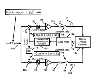
[0054] Figure 1 is a simplified block diagram of an M-PSK receiver,
according to one
embodiment.
[0055] Figure 2 is a graph of one embodiment of g2(0), a base
function for BPSK.
[0056] Figure 3 is a graph of one embodiment of g4(0), the base function
for QPSK.
[0057] Figure 4 is a block diagram of a phase determiner
communicatively coupled to a
metric generator, according to one embodiment.
[0058] Figures 5 and 10 are schematics of exemplary circuitry that
can be used to
implement embodiments of a metric generator used to evaluate the base
function, gm (6).
[0059] Figure 6 is exemplary SystemVerilog code that can be used to
implement one or
more embodiments of the metric generator.
[0060] Figure 7 is a graph illustrating performance of various
embodiments of a phase
detector compared to that of several prior art phase detectors.
[0061] Figure 8 is a graph illustrating normalized gains of
embodiments of the phase
detector compared to normalized gains of several prior art phase detectors.
[0062] Figure 9 is a graph of a principal angle, Op, relative to an
input phase, 6.
[0063] Figure 11 is an exemplary constellation diagram for Rectangular
QAM-32.
-10-
CA 02811457 2013-03-15
WO 2012/058757
PCT/CA2011/001217
DETAILED DESCRIPTION
[0064] Carrier phase error elimination in M-PSK receivers is usually
achieved via one of
two methods. The first technique uses a feedforward phase estimator to
estimate the phase error,
and that estimate is then used to demodulate the received and modulated
signal. The second
technique is the use of feedback, namely the removal the carrier phase error
using a Phase
Locked Loop (PLL) that attempts to cancel the phase error between the local
and received
carriers.
[0065] Carrier synchronization Phase Lock Loops (PLLs) obtain an
estimate of the phase
error via a carrier Phase Detector (PD). There are two general types of PDs:
Non Data Aided
(NDA) and Decision Directed (DD). One common problem with the DD and NDA
detectors is
that their gain is strongly dependent upon the input signal levels and the AGC
(Automatic Gain
Control) circuit's operating point and performance. If the PD's gain is
variable with one or both
of signal level and AGC performance, this means that the carrier PLL's
characteristics will vary
accordingly, which means that a non-optimal AGC causes a similar non-
optimality of the
performance of the carrier PLL.
[0066] The following embodiments are directed at NDA phase detector
structures for
carrier synchronization for M-PSK or other modulations. These detectors allow
the carrier PLL
to become nearly independent of the AGC and signal levels while enjoying
relatively good
performance. Unlike conventional phase detectors, some of the following
embodiments can be
implemented relatively compactly, allowing them to be practically deployed
using devices such
as an FPGA (Field Programmable Gate Array) or ASIC (Application Specific
Integrated
Circuit). Additionally, the following embodiments allow multiple modulations
to be supported
by the same receiver with relatively little added complexity in order to
support multiple
modulations. The phase detector includes a metric generator into which is
input the recovered
instantaneous phase of a symbol used to modulate the modulated carrier. The
metric generator
generates a metric that is a function of a phase difference between a
modulated carrier and a local
carrier.
System Model
-11-
CA 02811457 2013-03-15
WO 2012/058757
PCT/CA2011/001217
[0067] A simplified diagram of the front-end of a receiver under
discussion is shown in
Figure 1. 1/T is the symbol rate and, as well in the exemplary embodiment, the
sample rate. For
the exemplary embodiment, a PSK (Phase Shift Keying) signal is assumed for
simplicity. The
transmitted baseband PSK signal is m(t) .- En- anp(t ¨ nT), with p(t) being
the pulse shape
and the symbols being aõ = exp( On), with On= 27r = mõ I M being the ideal
symbol phases of the
transmitted baseband symbols, with mn E {0,1,...,M ¨I} (i.e., the phases are
uniformly distributed
in the interval [0, 2g) ), where M is called the modulation order or
modulation index (e.g. M=2
for BPSK (Binary Phase Shift Keying), M=4 for QPSK (Quaternary Phase Shift
Keying), M=8
for 8-PSK, etc.). In alternative embodiments other phases are possible for
different Ms which
may be different from those used here in the exemplary embodiment. In general,
for such
constellations as M-PSK in which the distinct ideal symbol phases are
uniformly distributed
within any continuous angular interval spanning 2n, M is the number of
distinct ideal symbol
phases of the symbols in the modulation's constellation diagram. By "uniformly
distributed", it is
meant that the phase difference between any two symbols of the modulation's
constellation
diagram is 2nk/M, where k is an integer. In other embodiments such as for
Rectangular QAM-
32 (wherein QAM is Quadrature Amplitude Modulation) as shown in Figure 11, the
modulation
order M for the purposes of defining the phase detector is the number of
orders of rotational
symmetry that the constellation diagram of the modulation has so long as the
constellation
diagram has at least two orders of rotational symmetry (i.e. has twofold
rotational symmetry).
For example, for Rectangular QAM-32 as shown in Figure 11, the constellation
diagram has
fourfold rotational symmetry, and accordingly M=4. In general, a modulation's
constellation has
M-fold rotational symmetry if the smallest nonzero positive angle in radians
by which the
constellation may be rotated in the I-Q plane and which results in the same
constellation form in
the I-Q plane is 27c/M . For example, as seen in Figure 11, the angle ff12 is
the smallest
positive nonzero angle in radians for which a rotation of the QAM-32
constellation in Figure 11
results in the same constellation form. Hence, for the constellation in Figure
11, M=4.
[0068] The modulated signal 100 that is present at the output of the
receiver's
intermediate frequency (IF) downconversion stage is Re[m(t)exp(jcoit+
j6),)1+n(t) , where n(t) is
the noise process, with co, being the received IF carrier frequency in
radians/sec, and 6?, (in
-12-
CA 02811457 2013-03-15
WO 2012/058757
PCT/CA2011/001217
radians) being the phase of the received IF carrier. In alternative
embodiments the receiver may
not have an intermediate frequency, or may have several intermediate
frequencies, in which case
appropriate modifications need to be made to the exemplary embodiments. Hence,
the
description of the exemplary embodiments should not be construed as limiting.
[0069] Alternative embodiments can be conceived in order to handle
modulations that
are related to M-PSK, such as O-MPSK (Offset MPSK), D-O-MPSK (Differential
Offset
MPSK), MSK (Minimum Shift Keying), GMSK (Gaussian Minimum Shift Keying), g 1 M
-
MPSK,
IM -MPSK (Differential gl M -MPSK), FQPSK (Feher's QPSK), 327- I M -8PSK,
D- 37r /M -8PSK (Differential 37r /M -8PSK), QAM (Quadrature Amplitude
Modulation),
OQAM (Offset QAM), PAM-PSK (Pulse Amplitude Modulation Phase Shift Keying),
Offset-
PAM-PSK, CPM (Continuous Phase Modulation) and its variants, and Trellis Coded
Modulation
(TCM) and its variants.
[0070]
In the following, for the purpose of describing the exemplary embodiment,
unless
otherwise stated the description of the exemplary embodiment assumes an M-PSK
signal
wherein M is a positive integer power of 2, i.e. M equals 21', wherein k is a
positive integer.
However alternative embodiments are possible for other modulation types, as
mentioned above.
[0071]
The matched filters 120, 135 response is p*(¨t) (where "*" denotes complex
conjugation), 0, (radians) is the phase of the receiver local carrier 165, and
wo =to, A-Aco
(radians/sec) is the local carrier frequency Ow is the frequency error between
the received and
local carriers in radians/sec). A quadrature receiver front end is assumed for
the demodulator of
the exemplary embodiment, i.e. multiplication by multipliers 105, 110 by the
local carrier and its
quadrature which is generated by passing the local carrier through a 90 degree
phase shifter 115.
Alternative embodiments may use other types of receiver front ends and,
accordingly the
exemplary embodiment presented here should not be construed as limiting. The
local oscillator
165 in the exemplary embodiment is controlled by the output of the loop filter
162 which has as
its input the output of the carrier phase detector 160. However, in
alternative embodiments the
oscillator may be controlled or may be free running, depending on the receiver
architecture, and,
moreover, the receiver structure may be implemented in analog, digital, or
mixed logic, etcetera.
Moreover, the phase detector may be used in embodiments employing feedback or
feed-forward
-13-
CA 02811457 2013-03-15
WO 2012/058757
PCT/CA2011/001217
architectures or combinations thereof. For the purposes of describing this
embodiment, symbol
timing synchronization is assumed, and the Nyquist criterion for zero 1St is
assumed obeyed at
the outputs of the matched filters 120, 135. Optionally, amplifiers 125, 140
are included after the
matched filters 120, 135. The quantity K for the amplifiers 125, 140 may be a
true amplification
or it may be a mathematical equivalent (preferably AGC-controlled) I-Q arm
gain. In many
receivers, K is a slow function of time, and is controlled by the AGC in order
to attain the
desired signal level at the inputs of the I and Q samplers so that they are
not saturated yet their
full dynamic range is utilized. The 1(0 and Q(t) signals are sampled by
samplers 130, 145, which
operate at a rate of preferably at least 1/T Hertz, from which the relevant
samples spaced 1/T
seconds apart (corresponding to optimal sampling instances for each symbol)
are extracted for
the structures of this embodiment. In an alternative embodiments the sampling
rate could be
higher than 1/T Hertz. In such cases, the samples that correspond to the
baseband symbols are
extracted, preferably either via sample selection, or via interpolation, or
both; the samples that
are used ideally, but do not necessarily, correspond to the ideal sampling
instances for the
received symbols. These ideal sampling instances are usually determined via a
symbol sampling
synchronization or determination circuit that is contained within the
receiver. In yet other
embodiments, the sampling rate may be less than 1/T. In such cases, the
structures presented
herein would operate upon a subset of the received symbols, which is also
possible .
[0072]
The notations n1 (t) and no (t) refer to the noise present before the (actual
or
equivalent) amplifiers 125, 140 in the I and Q arms, respectively. In many
systems, this noise
signal's source is an Additive White Gaussian Noise (AWGN) that is present in
the channel, an
assumption that is made for the purposes of describing this embodiment.
[0073] Following sampling, 1(n)=K(2Es-cos (¨Aco-
nT+0,+0,)+ni(n7)) 150 and
Q(n)=-K(2Es -sin (¨Aco=nT+0,+0)+110(nT)) 155 are generated, with 6e8iGo and
n,(nT),nQ(nT)¨ N(0,2NõEs), where Es ¨1 flp(t)12 dt is the symbol energy and
No/2 is the
2 '
AWGN power spectral density. The phase of the received (complex) baseband
symbol
rõ-----1(n)+M(n) is con tan -I (Q(n)1 1(n)), which as discussed in more detail
below is the
-14-
CA 02811457 2013-03-15
WO 2012/058757
PCT/CA2011/001217
instantaneous phase of the received baseband symbol 405 ("received phase"). In
polar
coordinates, rn = Irdexp(jccon).
[0074] Without loss of generality, for mathematical convenience it can
be assumed that
Vn , On = 0, whereupon:
=
con tan ii_Qt(n)\ =tan_i sm(¨Aco = nT +69+ nQ(nT)I (2Es)
(1)
1(n) cos(¨Aco = nT + 0,)+ ni(nnl (2E
s
[0075] The received phase g 405 is independent of the value of K of the
amplifiers 125,
140, as can be seen by the fact that K does not appear in (1). Since the
exemplary embodiments
rely on operations upon con 405, this means that the embodiments herein do not
depend upon K
nor upon the AGC's control of K. This is advantageous, since the AGC is
usually non-ideal and
the value of K usually does fluctuate. The only dependence on the AGC is
indirect and weak,
and will manifest itself if the AGC is so bad that I(t) 128 and Q(t) 142 are
either overdriven or
underdriven, which will cause one or more of the effects known by those
skilled in the art as
saturation, compression, and quantization noise to be significant. However,
usually the AGC can
easily be made to be sufficiently robust in order to prevent frequent
occurrences of overdriving
and underdriving, so that the independence of the exemplary embodiment from K
is a real and
substantial advantage in practice.
[0076] Let:
AOn = yon ¨ (¨Acon T +) (2)
[0077] Since it has been assumed for mathematical convenience in a non-
limiting manner
that V n,On = 0, the physical meaning of AO, is clear: it is the phase error
in the received phase
of any one of the received baseband symbols, co, 405, relative to the symbol's
ideal phase 0,,
that can be attributed to noise, ni(nT) and nQ(nT) (to see this, substitute
n,(nT)= no,(nT)= 0 in
the expressions for I(n) and Q(n), and then go, = tan1Q(n)1 I (n)) =
40õ = con ¨(¨AconT + 0,)= 0). AO, as defined in (2) is distributed as a Rician
phase pdf
(probability distribution function) given by:
-15-
CA 02811457 2013-03-15
WO 2012/058757
PCT/CA2011/001217
Pc (A01 X) P (AO, A0lEs / No =
cos0{0,12%
= 1+j2,' cos (A0)exp(x=cos2(A0))= f e-v2/2dy
(3)
277.
where ¨7T A0 7/".
Implementation of the Phase Determiner 400
[0078]
A phase determiner 400 in the form an inverse tangent function is used to
generate con 405. Although in the depicted embodiments the inverse tangent
function is used to
implement the phase determiner 400, in alternative embodiments (not depicted)
the phase
determiner 400 may be implemented in a different manner, and not necessarily
using the inverse
tangent function. The phase determiner 400 can be the same one used for
determining the signal
phase for subsequently making decisions upon the received symbols (a common
task in
demodulators). Moreover, con 405 can be used elsewhere in the receiver
regardless of the value
of M. Therefore, if structures are implemented for various Ms in the same
receiver, such as in a
receiver that has support for several modulations, the receiver may use one
instance of the phase
determiner 400. This reduces the resources needed and is another advantage of
the exemplary
embodiment. The inverse tangent in the exemplary embodiment is one whose range
is [¨II-, 7T),
that is, it takes into account the quadrant in which rn is present. For
example, it behaves
similarly to the function atan2 in the program MatlabTM.
Phase Detector
[0079]
Figures 2 and 3 show embodiments for BPSK and QPSK, respectively, of a base
function used to generate the metric that is a function of the phase
difference between the
modulated and local carriers. In the embodiments depicted in Figures 2 and 3,
the base function
is denoted g (0) , where 0 is an input variable representing an angle in
radians and where M
is the modulation order, and has a curve that is a triangle wave with
periodicity of 2r IM
radians. When used to generate the metric, co, 405 in radians is input to the
base function, and
g (con) is evaluated. The triangle wave includes positively and negatively
sloped linear
-16-
CA 02811457 2013-03-15
WO 2012/058757
PCT/CA2011/001217
segments that connect to each other at the triangle wave's maxima and minima.
The absolute
values of the slopes of the positively and negatively sloped segments have
identical absolute
values.
The zero-crossings of the positively sloped linear segments in the depicted
embodiments, which correspond to the stable PLL equilibrium points in the
exemplary
embodiment, result when y6. 405 is one of the ideal symbol phases and when the
modulation
used utilizes uniformly distributed symbol phases within any continuous
angular interval
spanning 27r radians, as is the case with BPSK and QPSK; that is, in the
depicted embodiments,
when there is zero phase error, the output of the base function is zero. For
example, for BPSK
(M=2), see Figure 2. For QPSK (M=4), see Figure 3. gm (0) is defined through
the periodic
extension of its input value over the entire range of 9 E (-00,00) (that is,
taking into account
that every phase can be expressed as itself plus any integer multiple of 2r),
but the range of
interest and implementation of gm (9) for the current embodiment is chosen to
be 0 E 7)
radians since this covers the entire unique angle range of 27r . An
alternative embodiment is with
the stable equilibrium point positioned at the zero crossings of the negative-
sloped lines.
Alternative embodiments of gm (0) may be such that their stable equilibrium
points are any set
of M points that are uniformly spaced in the interval 0 E [-Tr, 7t) with a
spacing of 27 I M ; in
particular, in the case where those phases do not correspond to the ideal
symbol phases, the
symbol decision logic in the receiver should be such that it takes this into
account, as known to
those skilled in the art. It is also noted that any angle can of course be
expressed as itself plus any
integer multiple of 2r. Thus, in alternative embodiments, the angles can be
defined as residing
in any interval of at least length 21r (which usually would be a continuous
interval (for
simplicity) but not necessarily so), in which case this entails a
corresponding adaptation of the
definition of g õ (8). In the present embodiment, gm (9) has a maximum of 1
and a minimum
of -1. In other embodiments, gm (0) may have a maximum and minimum with
different values,
such as A for the maximum and -A for the minimum, where "A" is some non-zero
value. In
general, the maxima and minima of gm (9) will have identical absolute values
(in the
exemplary embodiment, for example, the value of this absolute value is "1").
In some
embodiments gm (0) may have a DC offset, either inevitable (e.g. due to
quantization) or
-17-
CA 02811457 2013-03-15
WO 2012/058757
PCT/CA2011/001217
intentional, that is for example the maximum will be A+DC and the minimum will
be (-A+DC),
where "DC" represents the DC offset. However, excessive DC offsets may cause
performance
degradations.
[0080]
For some modulations, such as some instances of circular QAM and some
instances of PAM-PSK (Pulse Amplitude Modulation Phase Shift Keying), the
modulation may
have two or more-fold rotational symmetry and the distinct ideal symbol phases
of the
modulation may be uniformly distributed. It may be possible to use multiple
values of M when
evaluating the base function gm (0) for such modulations. For example, the
modulation may
have M-fold rotational symmetry where M is a first value, and the modulation's
constellation
diagram may have M distinct ideal symbol phases, where M is a second value
that differs from
the first value. For example, this is true for certain constellations of
circular QAM and PAM-
PSK. For such modulations, it is within the purview of a skilled person to
select which value of
M is better to use when determining the appropriate base function gm (0) .
[0081]
A useful attribute of the triangular phase detector is that with clever
implementation that takes advantage of the linear characteristic of the curves
of gm (0) , the
implementations of certain embodiments of gm (0) can be made to consume
relatively few
hardware resources. As already noted, the phase determiner 400 can be the same
one used for
decisions upon the received symbols, and therefore by using these phase
detectors a relatively
efficient implementation can be achieved, especially when multiple modulations
are desired.
[0082] As a preliminary step, for the exemplary embodiment, the phase 8 is
encoded
using a suitable encoding such as two's complement encoding which is b bits
wide, in the
exemplary embodiment from bits b ¨1 (the MSB (Most Significant Bit)) to 0 the
LSB (Least
Significant Bit). In the exemplary embodiment the MSB is the sign bit. The
notation 0 [x] is
used in order to refer to significant bit number "x" in the binary
representation of 0 . "x" is not
necessarily the bit with index "x" counting from the right (as is the case in
two's complement,
starting with bit 0 as the LSB); in general, 0 [0] would refer to the LSB, 0
[1] would refer to
the bit which is of the least significance except for the LSB, 0 [2] would
refer to the bit that is of
-18-
CA 02811457 2013-03-15
WO 2012/058757
PCT/CA2011/001217
the least significance except for 0 [1] and 0 [0], etcetera. For example, for
the exemplary
embodiment, e[b ¨1] is the sign bit and MSB, and 0[0] is the LSB. The notation
6/[x : y] is
used to denote the binary number formed by the sequence of bits 8[x], O[x ¨11,
¨ 21,
9[y]. For example, 0[3: 01 signifies the binary number composed of the bits
0[3],
0[2], 8[1], 0[0] (e.g., if the code representing 0 is 1 1 1 10011 then 0[3 :
01 -= 0011 in
this case). Additionally, the codes are assigned to linearly encompass the
entire angular range,
i.e. [¨IT, Tr) radians. That is, the lowest possible code (= the most negative
code) represents the
angle
radians, and the highest possible encoding (= the most positive code)
represents
¨ 6 radians, where 6 = 7r (2b-1) . To give a few examples, if there are b = 8
bits in the
code, the code "10000000" represents the angle ¨7 , the code "10000001"
represents the
number -7 7 1128 , "10000010" represents the angle -7 27r /128 and soon;
the code
"00000000" represents the angle 0, the code "00000001" represents the angle
711128, the code
"00000010" represents the angle 271-/128, and so on, and the highest code
01111111
represents the angle 1277r/128= 7T ¨ 71" 1128 = ir ¨ IT 1(2"-i) . The purpose
of this encoding is
twofold. First, it maximizes the dynamic range utilization of the binary
representation; since the
angular range is [¨Tr, 7) radians, the binary encoding encompasses this range
and no codes are
wasted. Hence quantization noise is minimized and the dynamic range of the
binary
representation is fully utilized. Secondly, as shall be seen below this is one
way in which a
relatively efficient implementation of g (P) can be obtained. Other encodings,
such as one's-
complement and sign-magnitude encoding can also similarly be used in other
embodiments to
attain similar efficiencies; the chosen encoding may, but does not need to,
linearly encompass
substantially all of the possible phases. It is also noted that the position
of the LSB (which is the
/east significant) and MSB (which is the most significant) within the code
word, as well as the
position of the intermediate bits may depend on the encoding scheme used,
which may vary from
embodiment to embodiment. Additionally, for convenience the concatenation
operation is
defined as <x,y> which signifies the concatenation of the binary numbers x and
y. For example,
<0101,1111> is the binary number 01011111.
-19-
CA 02811457 2013-03-15
WO 2012/058757
PCT/CA2011/001217
[0083] To see how it is possible to efficiently implement gm (4) ,
note the linear
characteristic of the base function gm (6) at each interval of length IT
1(2M), e.g. for BPSK
the intervals are [¨IT, ¨3;z- / 4) , [-37z- /
/ 2) , [-71-12,¨ff / 4) , / 4,0) , [0,71- / 4),
[77-/ 4,7T I 2) , [if/ 2,377- / 4) , [37z- / 4,7T) , as can be seen in Figure
9. In each of these intervals
the characteristic of gm (P) is completely linear and has the same polarity.
This can be
exploited by cleverly encoding the angle, for example in two's complement
notation, in order to
implement the phase detection characteristic.
[0084] First, a principal angle is defined as:
0 mod (ff/(2M))
[0085] 0 =
g/(2M) (4)
[0086] Note that the "mod" (modulo) function is defined such that the
value of Op is
positive and is between 0 and 1, i.e. its range is [0,1). That is, the infimum
of Op is 0 and the
supremum of Op is 1. An example of Op for BPSK can be seen in Figure 9.
[0087] Now, tables of the value of g2(0) as a function of Op and g4(6)
as a
function of Op are constructed, as shown below.
-20-
CA 02811457 2013-03-15
WO 2012/058757
PCT/CA2011/001217
Table 1 - Value of g2 (9) as a function of Op
Value of Op Addition to 6[b¨I1 Bp ¨ 2] O[b ¨ 3]
Angular Interval g2 (0) as a Multiplier 9,, or
for input variable
function of
9
Op
[¨Tr, ¨3/r / 4) Op 1 0 1 0 0
[-37/ 4,-7 / 2) 1-0,, -1 1 1 0 1
[-7 / 2,-7-c/4) -0, -1 0 1 1 0
[¨,r/4,O) -1+0,, 1 -1 1 1 1
[0,7/ 4) 0,, 1 0 0 0 0
[7/4,7/2) 1-9g. -1 1 0 0 1
[7/2,37r/4) -0,, -1 0 0 1 0
[3r/4,) -1+0,, 1 -I 0 1 1
-21-
CA 02811457 2013-03-15
WO 2012/058757 PCT/CA2011/001217
Table 2 - Value of g4(&) as a function of Op
Value of 6,, Addition 9[b -I] Op - 2] 8[b-31
O[b - 4]
Angular Interval g4(9) as Multiplier to 1 9 , or
for input variable
a function
0
of Op
[¨n- ,-7 g 1 8)e p 1 0 1 0 0 0
[-777-18,-377-14) 1-0,, -1 1 1 0 0 1
[-371- I 4, ¨572- 1 8) -9,, -1 0 1 0 1 0
[-571-/ 8,¨ff / 2) -1+0,, 1 -1 1 0 1 1
[¨Tr/ 2, ¨377-/ 8) 9, 1 0 1 1 0 0
[-37r/8,-7/4) 1-8,, -1 1 1 1 0 1
-0,, -1 0 1 1 1 0
Pr/8,0) -1+0,, 1 -1 1 1 1 1
[0,77- / 8) 0,, 1 0 0 0 0 0
[7r/8,7r/4) 1-0p -1 1 0 0 0 1
[71- / 4,371- / 8) -0,, -1 0 0 0 1 0
[37r/ 8,77-/ 2) -1+ep 1 -1 0 0 1 I
Pr/ 2,57r/8) 0,, 1 0 0 1 0 0
[5n-/ 8, 3ff / 4) 1-8,, -1 1 0 1 0 1
[37/4,77r/8) -0,, -1 0 0 1 1 0
[777-/8,71) -1+0,, 1 -1 0 1 1 I
[0088] For a compact hardware implementation, note that, in two's
complement notation
of b bits, up to an inaccuracy of the LSB, in order to compute the phase
detector (assuming the
MSB is bit b-1 and the LSB is bit 0):
-22-
CA 02811457 2013-03-15
WO 2012/058757
PCT/CA2011/001217
I.
Op is the signed binary two's complement number <0,0[6-3 ¨ log, M : 0] >
(concatenation of "0" and O[b ¨3¨ log 2 M : 0]), where it is understood that
in the numerical
encoding convention chosen by the designer the range of 8, is [0,1) (or as
close to that
range as can be expressed by the resolution of the quantization of Op).
2. Op is either inverted or not according to bits O[b ¨ log2 M ¨ 1 : b ¨ log2
M ¨ 2] of 0, for
example as seen in Table 1 and Table 2.
3. Either 1, -1 or 0 (or as close to those values as can be expressed by the
resolution of
the quantization) is added to Op or its inverse according to bits
O[b ¨ log, M ¨1: b ¨ log2 M ¨ 21, for example as seen in Table 1 and Table 2.
[0089] In this way, multiplications and any other complicated operations
can be avoided,
and there is no need for lookup tables. The base function can be implemented
using elementary
gates, multiplexers, and additions. Moreover, the overhead for generating a
phase detector for a
different modulation is quite minimal, since no new computation of 0 is
necessary.
[0090]
A schematic illustration of the efficient hardware implementation for
computation
of g (0) for an exemplary embodiment is shown in Figure 5. From the input
variable 0 500,
which is in the exemplary embodiment expressed as a two's complement binary
fixed point
notation, the bits whose indices O[b ¨ 2 ¨ log, M] 512 and O[b ¨1¨ log, M] 510
are passed through
an exclusive OR (XOR) gate 520 and the resulting signal 530 is passed through
an array of XOR
gates 540 with bits <0, /9[1, ¨3 ¨ log2 M : 01> (concatenation of "0" and O[b
¨ 3 ¨ log, M : 01) 505. This
is done via XOR gates between each of the bits of <0, 60[b ¨ 3 ¨ log, M :01>
505 and the signal 530.
The array of XOR gates 540 is represented by a single XOR symbol (but which,
it is made clear,
reflects the aforementioned bitwise XOR). Collectively, the XOR gates 520, 540
act as inverting
hardware that invert Op depending on the value of bits O[b ¨ 2 ¨ log2 M] 512
and O[b ¨1¨ log2 M]
510. The bits having indices O[b ¨ log, M ¨1 : b ¨ log, M ¨ 2] 515, 512, are
used to control the
selection input of data selection hardware such as a multiplexer 550. The
output 555 of the
multiplexer 550 contains the constant 1, -1, or 0, which is added to Op or ¨Op
in order to form
-23-
CA 02811457 2013-03-15
WO 2012/058757
PCT/CA2011/001217
gA, (0), as shown for example for BPSK and QPSK in Table 1 and Table 2,
respectively, and as
discussed above. The value of Op or 9p,¨
as used to form gm (9) as shown for example for
BPSK and QPSK in Table 1 and Table 2, respectively, is the signal 545 that is
output from the
array of XOR gates 540. The value of gm (9) 565 is generated by the summation
by adding
hardware such as an adder 560 of the output 555 of the multiplexer 550 and the
output 545 of the
array of XOR gates 540. This summation complies with all the rules for
summation of signals, as
appropriate for the chosen encoding (two's complement in the exemplary
embodiment).
[0091]
This implementation of gm (41) , the metric generator 410, is the one that is
used
in order to generate the metric gm (c ,) 415, where con 405 is the input to
that function block as
used in the exemplary embodiment, as shown in Figure 4. The angle g is encoded
in the same
manner as discussed for 0 above.
[0092]
For the exemplary embodiment, even though the input of gm (0) by convention
signified the range [¨IT, 7r), the output by convention spans the range [-1,1)
. However, this is
not necessarily the case in alternative embodiments. The range which the
numerical encodings
span is defined according to the designer's choice; for other embodiments, the
output of gm (6)
could span other ranges than ]-1,1) .
[0093]
A SystemVerilog implementation of gm (0) for various values of M, which
requires no multiplications or other complicated operations, nor any
significantly size lookup
table, is shown in Figure 6. The values of M supported by this implementation
are M=2, M=4,
M=8, and M=16. The input to the function is the input -theta-, in two's
complement notation.
The phase detector outputs are in Al l_PD_values [num_modulations -1: 0], also
in two's
complement notation (format is (width bits, from MSB to LSB): 1 sign bit, 1
whole bit,
fraction bits). A selected output PD value in two's complement is also
provided (format is
(width bits, from MSB to LSB): 1 sign bit, fraction bits), which is selected
by the input
log2M_minus_l (which is 0 for M=2, 1 for M=4, 2 for M=8, and 3 for M=16).
Figure 6 also
-24-
CA 02811457 2013-03-15
WO 2012/058757
PCT/CA2011/001217
shows how practical issues such as sign extension and binary point alignment
are handled for
operations such as inversion and addition of the various quantities.
[0094]
Although in the exemplary embodiment a signed two's complement notation is
used, other numerical representations can be used, including but not limited
to one or more of
floating point and other fixed point or variable point notations, and non-
binary encodings.
[0095]
Strictly speaking obtaining the negative of a number in two's complement
notation, i.e. obtaining -x for a number x, is performed via (¨x)+1, where "¨"
represents bitwise
inversion. The procedure described above and in Figures 5 and 6 may be
modified to take this
into account in alternative embodiments. Due to the asymmetric nature of two's
complement
encoding (i.e. that there is one more of the negative values than of the
positive values) in many
systems (especially signal-processing structures) -x is calculated simply as
(¨x) in order to avoid
potential overflow problems and in order to simplify logic. This is the
procedure adopted for all
the exemplary embodiments for two's complement representation.
Implementation of g m (6) for alternative embodiments
[0096] In general, for alternative embodiments, a proportionality constant
and modulo
function ranges are chosen so that Op is between 0 and A, i.e. the range of
(9p is [0,A), where A
is the absolute value of the maximum of the function gõ (4) . That is, the
infimum of Op is 0
and the supremum of Op is A.
The normalization in such cases would be
moder/(2M))
0 A =
/(2M) . For example, for BPSK:
7r
-25-
CA 02811457 2013-03-15
WO 2012/058757
PCT/CA2011/001217
Table 3 - Value of g2 (6) as a function of Op for alternative embodiment where
the maximum
value of g2 (0) is A
Value of Or Addition to 9[b-1I O[b ¨ 2] Oh, ¨ 3]
Angular Interval g2(8) as a Multiplier Or or
for input variable
function of
0
Op
[-TC,-37z- / 4) 9, 1 0 1 0 0
[-37-c/ 4,--7-c/ 2) A-ep -1 A 1 o 1
[¨n-/ 2,¨g/ 4) -ep -1 0 1 1 0
[¨/4,O) -A+9 1 -A 1 1 1
[0,7c/ 4) Op 1 0 0 0 0
[71-/4,7r/2) A-Or 1 A 0 0 I
[7r/2,37r/4) -0, -1 0 0 1 0
[371-/ 4,70 -A+& i, 1 -A o 1 1
-26-
CA 02811457 2013-03-15
WO 2012/058757
PCT/CA2011/001217
[0097]
Similar tables can be constructed for other values of M and other modulations.
These tables allow us to reach a relatively efficient implementation for the
metric generator, as
follows.
[0098] For a compact implementation for the exemplary embodiment, note
that, in two's
complement notation of b bits, up to an inaccuracy of the LSB (Least
Significant Bit), in order to
compute the base function (again, assuming the MSB (Most Significant Bit) is
the bit of index
b-1 and the LSB is the bit of index 0):
1.0, is B multiplied by a signed binary two's complement number <009[b ¨3 ¨
log, M :01>
(concatenation of "0" and 8[1)-3¨ log, M :0]), where B is a proportionality
constant such
that the range of G. is [0,A) according to the numerical encoding convention
chosen by
the designer (or as close to that range as can be expressed by the resolution
of the
quantization of Op)).
2. 9, is either inverted or not, according to bits G[b ¨log,M ¨1: b ¨ log,M
¨2] of 9, for
example as seen in Table 3.
3. Either A, -A or 0 (or as close to those values as can be expressed by the
resolution of
the quantization) is added to Op or its inverse according to bits
¨ log,M ¨1:b¨log2M ¨2], for example as seen in Table 3.
[0099]
Also, for convenience, the "principal angle precursor" is defined as
<0, O[b ¨3 ¨ log2 M :01> for two's complement notation. In this case, it is
clear from the above
definitions that Op is B multiplied by the principal angle precursor. In
embodiments in which
B equals one and the principal angle precursor is accordingly not amplified,
the principal angle
precursor and the principle angle are equal, as is the case for the embodiment
described in
relation to Tables 1 and 2, above. "Amplification" in the context of this
disclosure does not
necessarily mean that the amplitude increases; "amplification" by B in the
context of this
disclosure could also mean a reduction in amplitude (if B is less than 1) or
no change in
amplitude (if B equals 1).
-27-
CA 02811457 2013-03-15
WO 2012/058757 PCT/CA2011/001217
[00100]
A schematic illustration of an efficient implementation for computation of
g(0) for such embodiments is shown in Figure 10 From the input variable 0
1000, which in
the exemplary embodiment is expressed in two's complement binary fixed point
notation, the bits
whose indices are O[b ¨ 2 ¨ log, M1 1012 and Kb ¨1 ¨ logõ M] 1010 are passed
through an
exclusive OR (XOR) gate 1020 and the signal 1030 that results is passed
through an array of
exclusive OR gates 1040 with bits <0,19[b ¨3¨log2m :01> (concatenation of "0"
and
e[b ¨3¨ log2M :01), 1005. This is done via XOR gates between each of the bits
of
<0, ¨ 3 ¨ log 2 M :
1005 and the signal 1030, which is represented by a single XOR symbol
1040 (but which, it is made clear, reflects the aforementioned bitwise XOR).
The XOR gates
1020, 1040 represent the inverting hardware used to perform controlled
inversion. The bits
whose indices are O[b ¨ logõ M ¨1 : b ¨ log, M ¨ 2] 1015, 1012, are used to
control the selection
input of a data selector such as a multiplexer 1050. The output 1055 of that
multiplexer 1050
contains the constant A, -A, or 0 that is added to Op or ¨Op in order to
generate the metric
(0) , as shown for example for BPSK in Table 3 and as discussed above. The
value of Op or
0p,¨ as used to
generate the metric gm (0) as shown for example for BPSK in Table 3, is the
signal 1048 that is obtained by amplifying the result of the controlled
inversion via an
amplification device 1047 such as a multiplier or a bit shifter. The value of
the metric g m (0)
1065 is generated by the summation via adding hardware such as an adder 1060
of the output
1055 of the multiplexer 1050 and the output 1048 of the amplification device
1047. This
summation complies with all the rules for summation of signals, as appropriate
for the chosen
representation (e.g. two's complement in the exemplary embodiment). In the
case that the signal
at the output of the controlled inversion 1045 already has a supremum of A
according to the
numerical encoding convention chosen by the designer, then the amplification
device 1047 may
be omitted, that is, the output of the controlled inversion 1045 can be
connected directly to the
adding hardware 1060.
[00101]
In alternative embodiments, where in the various exemplary embodiments the
bits
O[b ¨3¨ log, M :0] are used, it is possible to use a plurality of the most
significant bits of those
bits, for example O[b ¨ 3 ¨ log, M :01 (all the most significant bits of O[b
¨3¨ log, M : 0] , as is done
-28-
CA 02811457 2013-03-15
WO 2012/058757
PCT/CA2011/001217
in the exemplary embodiments), or Kb ¨3 ¨ log, M :11 (all the most significant
bits of
O[b ¨3 ¨ log2 M :0] except the LSB), or O[b ¨ 3 ¨ log2 M :2] (all the most
significant bits of
O[b ¨ 3 ¨ log, M :0] except the two least significant bits), etc. In an
embodiment that differs from
the exemplary embodiment wherein not all the most significant bits of lib ¨3
¨10g2 M :0] are
used, appropriate modifications are made to other parts of the receiver to
accommodate the
number of bits used. Such embodiments may be useful when a further reduction
in resources is
desired; however, such embodiments may be more susceptible to quantization
noise.
Phase Detector Performance Analysis
[00102] The S-curve of the phase detector is computed via a Fourier
series representation
of gm (q),):
sin (M = (2k +1)cos )
Sm,x(69= E[gm(con)0,1= E n __ ee (5)
n" k=0 (2k +1)2
(note the implicit dependence upon 2, through yo,). Now, using:
(On A On (6)
[00103] And:
-29-
CA 02811457 2013-03-15
WO 2012/058757
PCT/CA2011/001217
S
[
= E (-1)k sin[M = (2k +1)(A0n + 61,))
(2k + 1)2 91
2 L _____________________________________
(sin(M = (2k + 0,64, )cos(M = (2k +1)60 \
= E
8L(-1)k +cos (M = (2k +1)A0, ) sin (M = (2k + __ e)
Be
k=0 (2k +1)2
E[sin (A/ = (2k +1)A0r, )cos(M = (2k +1)0, )19,1 (7)
8 - +E[cos(M = (2k +1)Aqin )sin(M = (2k +1)0e) Be]
k =0 (2k+1)2
8 - (E[cos(M = (2k +1)6,0,)]sin(M = (2k +1).9,)\
k =0 \ (2k+1)2
[00104] Given that:
-
y \ I((2k+1)M-1)/2 (2')
E[COS (A/ = (2k +1),A0n )] =\l'2x exP (8)
+1 )
q2k+1)M+1)/ 2 (z
2
[00105] where I n(*) is the n-th order modified Bessel function of the
first kind, the
following results:
((
sm.2(Oe),72 E(_0 2 expm 42k+
8 k _____________ 1)M-1)/2 k 2f y
pk+02 sin(M-(2k+1)0e) (9)
1c3 +I((2k+1)M+1)/2( X2)
[00106] As a useful approximation, using the fact that
\ ¨
'17 X = exp (-2X ) /((2k+I)M -1)12 (
> eXp (
T) high SNR -(2k+1)2 M2 )
2 4x (10)
+/((2k+1)21/ +I)/ 2 (f)
[00107] Then approximately at high SNR:
-30-
CA 02811457 2013-03-15
WO 2012/058757
PCT/CA2011/001217
8 '
SA4,0, (Ge ) a liM SA/ y (et, ) = -7D-1)k (exp(-A424(2,:+02)/(2k +1)2 ) sin(M
= (2k +1)8, ) (11)
''''
IT k=0
Expression (11) is useful for calculations at high SNR, since in some
numerical programs such as
MatlabTM the calculation of Bessel functions is sometimes not sufficiently
accurate at high
SNRs. The gain of the phase detector is:
_
/
tA' -'
as (4,)
c , ku = (1)k (r /u2k+om-0/2k 21 (.2k +02 m. (2k +0
8
00e 0 4) 7r2 W) 1 X
)
+I((2k+1)M+1)/2 0
e _
i (12)
i -
Ixl - \
TY
e,q1(_õjr) /u2k om-0/2k 21 (2k+1)
8=M ''' k si
x)
_
+/((2k+1)M+1)/ 2I 0 )_),
[001081 At high SNR:
8 . m- 00 (_ ok
Cf co a- 1 im CM x = ___
2 1 ______________________________________ (13)
i ,
7r k=0 (2k + l)
[00109] t 1 \k 7
Using L µ- ' = ' :
,,0(2k+1) 4
8 = M 7r 2M
CA1,0 = ____ i = _________________________________________________ (14)
-
,. 4
7z 7-z-
[00110] This can be verified graphically from the S-curve. The
normalized gain of the
phase detector is defined as:
i _
x - \
Cif 4 COIt,(2k+f)m-0/2 (-2)
a = ' ' = 1( 1)k 'I if x =exp(r)
k=0 /(2k +1) (15)
m x
2
X
M ,o0 +I42k +1) M +1)12 ( \ 2 ) Li
_
[00111] A graph of a, , is shown in Figure 8 (the squares, denoted as
the curves labeled
TRm, where M=2,4,8,16 for M-PSK; the black squares are theory, while the
transparent squares
are simulation) and it is compared to the normalized gain of the prior art
detector discussed in Y.
Linn, "Robust M-PSK phase detectors for carrier synchronization PLLs in
coherent receivers:
theory and simulations," IEEE Trans. Commun., vol. 57, no. 6, pp. 1794-1805,
Jun. 2009, which
-31-
CA 02811457 2016-09-30
is represented by triangles (computed via theory) and denoted by dm, where
M=2,4,8,16 for M-
PSK. As can be seen, the phase detector presented here has well-behaved
normalized gains.
[00112] The normalized equivalent loop noise at 9,, 0 is defined as:
N",x(n)E--- lim (g m (con) ¨ S m ,x(0,))1 C m
(16)
[00113] which is:
(
N, 2, (n) = 8" 1)A sin (M = (2k + 1)A0õ)\/2M
k =0 (2k +1)2 TC
(17)
4s1n (M = (2k + 1)40n
j 1) _____________
k =0 (2k+1)2
[00114] The PD's self noise is defined as:
2 = x = var(Nõ,, (n))
(18)
[00115] Substituting results in:
4 -sin( A/ = (2k +1)r) N2
= 2x = var(Nm,(n)) = 2 xf ¨ (-04 ________________________ Pc (T I X) = d r
(19)
k= 0 (2k + 1)2
[00116] One of the most widely accepted performance metrics of a phase
detector is the
phase-error variance var(9, ) (or equivalently, the loop-SNR p 1/ var(69 ) of
a PLL that uses
that phase detector. This is due to the fact that the phase-error variance has
an important role in
determining the cycle-slip rate of the carrier synchronization PLL and the SER
(Symbol Error
Rate). Determination of var(0,) via computer simulations is done using
nonlinear models.
[00117] To evaluate the performance of the foregoing embodiments of
the phase detector,
computer simulations are used in order determine var(ee) for various types of
phase detectors. In
Figure 7, the phase error variance obtained using the proposed phase detectors
(TR2, TR.4, TR8.
TR16 for M=2, M=4, M=8, and M=16, respectively, for M-PSK) is compared to the
M-th order
nonlinearity (c2, c4, ca. c16 for M=2, M=4, M=8, and M=16, respectively, for M-
PSK) and the
normalized M-th order nonlinearity detector (d2, da, da. d16 for M=2, M=4,
M=8, and M=16,
respectively, for M-PSK) discussed in Y. Linn, "Robust M-PSK phase detectors
for carrier
synchronization PLLs in coherent receivers: theory and simulations," IEEE
Trans. Commun.,
- 32 -
CA 02811457 2013-03-15
WO 2012/058757
PCT/CA2011/001217
vol. 57, no. 6, pp. 1794-1805, Jun. 2009. As can be seen, the proposed phase
detectors have
performance that is virtually identical to the normalized M-th order
nonlinearity detector, which
was shown to have best-in-class performance. Hence, the phase detectors
described in this
embodiment have excellent performance.
Reduction to Practice and Approximate Resource Usage Compared to Prior Art
[00118]
All the structures presented in this document have been implemented in
practice
and proven to work by the inventor using a Terasic DE2-115 board with an
Altera Cyclone IV
FPGA.
[00119]
The FPGA was also used to implement the phase detector disclosed in Y. Linn,
"Robust M-PSK phase detectors for carrier synchronization PLLs in coherent
receivers: theory
and simulations," IEEE Trans. Commun., vol. 57, no. 6, pp. 1794-1805, Jun.
2009, as a point of
comparison. In order to attain the comparison, several documents that
calculate the equivalent
gate count for FPGA structures were used as sources. These are documents
Altera Inc.
Application Note 110: Gate Counting Methodology for APEX 20K Devices, Sept.
1999, Xilinx
Inc. Application XAPP 059: Gate Count Capacity Metrics .for FPGAs, Feb. 1997
and M. H.
Rais, "Efficient Hardware Realization of Truncated Multipliers using FPGA,"
International
Journal of Engineering and Applied Sciences, vol. 4, no. 2, 2009. From those
sources, the
following approximate gate equivalences are obtained:
-33-
CA 02811457 2013-03-15
WO 2012/058757
PCT/CA2011/001217
Table 4
FPGA Structure Approximate Average Equivalent Gates
Logic Cell (LC) (Combinational Content) 10
Register 7.5
Embedded Memory Bit 4
Multiplier (8 bit x 8 bit) 500
[00120] Estimation of the number of gates from FPGA structures is an
imprecise science,
and those gate counts will differ from ASIC gate counts. Nonetheless, the
values in Table 4 are
useful for the purpose of making comparisons.
[00121] In the Altera Cyclone IV FPGA in the DE2-115 board used for
tests, the
following resource usage data was measured:
Table 5
Implementation Metric LCs Total
Memory Equivalent
Bits Gates
Prior Art for BPSK 32768 1
131082
Prior Art to Add QPSK 32768 1
131082
Prior Art to Add 8-PSK 32768 1
131082
Prior Art to Add 16-PSK 32768 1
131082
, , I
Total Prior Art for BPSK, QPSK 8-PSK and 16-PSK 131072 4
524328 I
Phase detector based on g2 (D) for BPSK 32768 5
131122
To add phase detector based on g, (0) for QPSK 0 5 50
To add phase detector based on g8 (0) for 8-PSK 0 5 50
To add phase detector based on g16(.) for 16-PSK 0 5 50
, I
Total Current Embodiment (structures based on 32768 20
131272 i
gm (e) )
[00122] Comparing the results, the total number of required gates has
decreased
substantially, by about 74.96%, i.e. only about 25% of the logic resources are
required as
compared to prior art (131272 equivalent gates as opposed to 524328 for prior
art). This also
allows for a similar and corresponding reduction in power consumption and
circuit area for the
embodiment as compared to prior art.
-34-
CA 02811457 2013-03-15
WO 2012/058757
PCT/CA2011/001217
[00123] As can be seen, the advantage of the present structures
increases as the number of
supported modulation increases, i.e. the advantage would be even greater if 5
or 6 modulations
(e.g. also 32-PSK and 64-PSK) were implemented as well.
[00124] The above comparisons were done in a fair manner, that is, the
chosen
quantization for the present structures and those of the prior art were chosen
so that both would
have roughly the same performance.
[00125] As discussed above, in some of the foregoing embodiments of the
phase detector,
clever coding of the numerical representation of the symbol phases allows the
phase detector to
be implemented relatively compactly. Moreover, the foregoing embodiments allow
for multiple
modulations to be supported by the carrier PLL, requiring relatively few
additional resources
when adding support for additional modulations. This is advantageous over
conventional phase
detectors.
[00126] The performance of the embodiments described herein in terms of
phase-error
variance (the most widely used metric used by those skilled in the art) may be
described in best-
in-class. Moreover, the foregoing embodiments provide phase detection which is
relatively
independent from AGC performance and of signal levels. This is advantageous
over many
conventional phase detectors.
[00127] In addition to the hardware implementations discussed above,
the foregoing
embodiments may be encoded on to a computer readable medium that is readable
by a processor
so as to configure the receiver to have the functionality described above. The
computer readable
medium may be flash memory, RAM, any other suitable disc or semiconductor
based memory,
or any other suitable computer readable medium. Using software to implement
the foregoing
embodiments may be suitable when an embodiment of the base function is used
that does not
lend itself to a relatively efficient hardware implementation, or when the
power consumption
advantages of hardware are immaterial, for example.
[00128] For the sake of convenience, the example embodiments above are
described as
various interconnected functional blocks, which may be implemented using one
or both of
distinct hardware and software modules. This is not necessary, however, and
there may be cases
-35-
CA 02811457 2013-03-15
WO 2012/058757
PCT/CA2011/001217
where these functional blocks or modules are equivalently aggregated into a
single logic device,
program or operation with unclear boundaries. In any event, the functional
blocks, software, and
hardware modules can be implemented by themselves, or in combination with
other operations in
one or both of hardware and software, or via any other suitable implementation
method.
[00129] While
particular example embodiments have been described in the foregoing, it is
to be understood that other embodiments are possible and are intended to be
included herein. It
will be clear to any person skilled in the art that modifications of and
adjustments to the
foregoing example embodiments, not shown, are possible
-36-