Note: Descriptions are shown in the official language in which they were submitted.
CA 02811542 2015-08-17
54373-11
Spectral band-pass filter having high selectivity and controlled polarization
PRIOR ART
Technical field of the invention
The present invention relates to a spectral filter having high selectivity and
controlled
polarization, especially for the production of filters in the infrared.
Prior art
A known conventional technique for carrying out a bandpass filtering function
consists
in stacking thin layers, taking care to choose the number, the thicknesses of
the layers and the
nature of the materials as a function of the template desired for the filter.
Patent application
W02008122431 describes for example such a filter, termed an interferential
filter. However,
once they involve a large number of thin layers, these hardware components
exhibit
brittleness as soon as they are subjected to cycles of temperature variations,
for example when
they are disposed in a cryostat, especially for applications in the infrared.
Indeed, these cycles
lead to destruction of the structure owing to the thermal expansion
coefficients which,
differing from one material to another and therefore from one layer to
another, induce
stresses. Furthermore, a filter operating in the infrared will require thicker
layers than a filter
operating in the visible, and thickness-related technological difficulties
will arise very rapidly,
said difficulties being made worse during the production of arrays of filters,
wherein it will be
necessary to vary the thicknesses from one filter to another.
Moreover, for certain applications, especially thermal detection, it may be
beneficial to
be able to analyze the polarization of the incident wave so as to distinguish
the type of object
detected. Hardware components based on the technology of the stacking of thin
layers do not
allow polarization-dependent selectivity.
It is also known to associate with a thin laver a dielectric grating (see for
example patent
application US5726805). This technique exhibits the advantage of using only a
single layer
but a filter produced by Mis technology can be nothing but bandstop when it is
used in
transmission.
An object of the invention consists in proposing a spectral filter that is
bandpass when it
is used in transmission, which exhibits strong wavelength-selectivity while
allowing control
of polarization.
1
CA 2811542 2017-04-27
81769930
SUMMARY OF THE INVENTION
According to a first aspect, the invention relates to a bandpass spectral
filter,
optimized for the transmission of an incident wave at at least one first given
central wavelength 4,
comprising: a metallic grating of thickness greater than about X0/50 and
comprising at least one
first assembly of substantially identical, parallel slits of width smaller
than about Xo / 10, spaced
apart in a periodic or quasi-periodic manner according to a first period
smaller than said first
central wavelength, a dielectric material layer of given thickness and given
refractive index,
coupled with the metallic grating to form a waveguide for the waves diffracted
by the grating, said
first period of the grating being suitably adapted so that only orders 0 and
1 of a wave at normal
incidence and wavelength X0 are diffracted in the dielectric material layer,
the dielectric layer and
grating assembly being suspended, in use, in a fluid of refractive index close
to 1 so as to obtain a
condition of total internal reflection at a dielectric layer-ambient medium
interface.
According to a first variant, the metallic grating is one-dimensional with a
single
assembly of parallel slits, forming a polarizing bandpass filter.
According to a second variant, the metallic grating is two-dimensional,
furthermore comprising a second assembly of substantially identical, parallel
slits, spaced apart in
a periodic or quasi-periodic manner according to a second period, the slits of
the second assembly
of slits being arranged in a different direction from those of the slits of
the first assembly.
According to an example of the second variant, the width of the slits of the
second
assembly of slits is substantially identical to that of the slits of the first
assembly of slits and the
two periods are identical. When the slits of the two assemblies of slits are
perpendicular, the filter
thus produced is strictly non-polarizing.
According to another example of the second variant, the two periods are
different
and the filter is optimized for the filtering of an incident wave at at least
one first and one second
central wavelength X01 and 42: the first and second periods are smaller than
the first and second
wavelengths respectively, and the period along each of the dimensions is
suitably adapted so that
only orders 0 and 1 of a wave at normal incidence and wavelength koi or 42
respectively are
diffracted in the dielectric material layer. The filter thus obtained is
polarizing and the filtered
wavelength depends on the polarization.
2
CA 02811542 2015-08-17
543/j-
According to a third variant, the metallic grating is two-dimensional,
comprising a
plurality of assemblies of substantially identical, parallel slits, spaced
apart in a periodic or
quasi-periodic manner, the slits of each of the assemblies of slits being
arranged along
different directions to form a pattern repeated along two directions, the
pattern being for
example hexagonal or parallelogram-shaped.
According to one or the other of the variants. the dielectric material layer
can be
structured according to a pattern substantially similar to that formed among
the slits of the
grating.
The thickness of the dielectric layer can be sufficiently thin to permit only
a single
guided mode in the dielectric layer at said at least one first central
wavelength.
Alternatively, the thickness of the dielectric layer is sufficiently thick to
allow the
propagation of several guided modes in the dielectric layer, allowing the
production of a filter
exhibiting several central transmission wavelengths.
According to an example, the material forming the dielectric layer comprises
one of the
materials chosen from among silicon nitride, silicon carbide, silicon oxide,
yttrium fluoride,
zinc sulfide, aluminum oxide or magnesium oxide.
According to an example, the material forming the grating comprises one of the
metals
chosen from among gold, aluminum, copper, tungsten, nickel, platinum, silver.
According to an example, the central wavelength lies between substantially
0.850 p.m
and 30 i.tm.
According to a variant, the spectral filter furthenmore comprises a substrate,
the
dielectric layer and metallic grating assembly being suspended on the rim of
an orifice formed
in said substrate.
According to a second aspect, the invention relates to a multispectral array
comprising
an assembly of spectral filters according to the first aspect, the gratings of
said spectral filters
being coupled with the same dielectric material layer, the dielectric layer
and metallic gratings
assembly of the filters being suspended on the rim of an orifice formed in one
and the same
substrate.
According to a third aspect, the invention relates to a near-infrared or
infrared optronie
detection system comprising a detector and a spectral filter according to the
first aspect or a
multispectral array according to the second aspect.
3
81769930 CA 2811542 2017-04-27
According to a variant, the optronic detection system furthermore comprises a
polarizer making it possible to polarize an incident wave in a direction
parallel to one of the
directions of the slits of the or of at least one of the metallic grating(s).
According to a fourth aspect, the invention relates to a method for the
fabrication of a spectral filter according to the first or the second aspect
or of a multispectral
array according to the first or the second aspect comprising: the deposition
on one of the faces
of the substrate of a silica layer and on the other face of the substrate of
the dielectric layer to
form the waveguide, the deposition of the metallic grating or gratings on said
dielectric
material layer according to a given pattern, the etching of the silica layer
at a rear face of the
substrate according to a pattern defined by UV lithography or electron beam
lithography,
aligned with the pattern of the grating or gratings formed in a front face of
the substrate, and
then the etching of the substrate from side to side, according to the given
pattern, so as to
obtain a suspended membrane formed of the dielectric layer and of the grating
or gratings.
According to a first variant, the deposition of the metallic grating or
gratings is
obtained after UV lithography or electron beam lithography.
According to a second variant, the deposition of the metallic grating or
gratings
is obtained after nano-printing.
When the dielectric material layer is structured, the etching of said layer
can
also be obtained after UV lithography or electron beam lithography, or after
nano-printing.
BRIEF DESCRIPTION OF THE DRAWINGS
Other advantages and characteristics of the invention will become apparent on
reading the description, illustrated by the following figures:
Figures lA and 1B, a diagram illustrating the principle of a bandpass filter
according to the invention and a variant of such a filter;
Figures 2A to 2C, three exemplary embodiments of a bandpass filter according
to the invention;
Figure 3, curves showing the spectral response calculated for a bandpass
filter
of the type of Figure 2A, for various values of period and of slit width;
4
CA 02811542 2015-08-17
54373-1 l
Figures 4A, 4B examples of implementation of a bandpass Filter of the type of
Figure 2C;
Figures 5A, 5B examples of two-dimensional gratings exhibiting hexagonal and
parallelogram-shaped patterns respectively;
Figure 6, a diagram of an exemplary multispectral array comprising a plurality
of
bandpass filters according to the invention;
Figure 7, a diagram showing an arrangement of gratings in an exemplary
multispectral
array;
Figure 8, a diagram showing an optronic detection system integrating a
spectral filter
according to the invention.
DETAILED DESCRIPTION
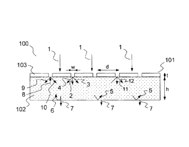
Figure IA illustrates by a diagram the principle of an exemplary bandpass
filter 100
according to the invention (sectional view) while Figures 2A to 2C represent
perspective
views of various exemplary embodiments. The filter 100 comprises a thin layer
102 of
dielectric material on which is deposited a metallic film 101 perforated
periodically, in one or
more directions, by a sub-wavelength pattern 103, the whole being suspended,
that is to say
not deposited on a substrate except in zones where the spectral filtering
functionality is not
sought. For example, the metallic film and dielectric layer assembly is
suspended on the rim
of an orifice formed in a substrate (not represented in Figure 1A). In use,
the stnicture is
therefore immersed in the ambient medium (vacuum or arbitrary fluid). The
layer 102 is made
of dielectric material transparent in the spectral band that one seeks to
transmit, for example
silicon nitride or silicon carbide. Other materials can be used such as for
example silicon
oxide, yttrium fluoride, zinc sulfide, aluminum oxide or magnesium oxide. The
metallic film
is for example gold, aluminum, copper, tungsten, nickel, platinum or silver,
it being possible
for the choice of the metal to be made so as to minimize the absorption in the
spectral range
of use. The elementary pattern 103 which is repeated in a periodic or quasi-
periodic manner
(that is to say with a slowly varying period) can comprise one or more narrow
slits stretching
right across the pattern. The grating can comprise an assembly of parallel
slits (case for
5
CA 02811542 2015-08-17
54373-11
example of Figure 2A) or two or more assemblies of parallel slits (case for
example of
Figures 2B and 2C for two assemblies of slits).
The principle of the filter relies on the confinement of an incident wave 1
(Figure 1A) in
the dielectric layer 102 which serves as waveguide, and then on its
transmission in the output
space (referenced output wave 7 in Figure IA). Trapping followed by
transmission are
obtained by virtue of the metallic diffracting structure 101 deposited on one
of the faces of the
waveguide 102, said structure moreover being suitable for the control of the
polarization, as
will be described subsequently. More precisely, the incident photons
(symbolized by the
arrow 1) are transmitted M the dielectric material layer 102 by diffraction
through the metallic
grating 101. This diffraction may take place at order 0, 1, etc. The
applicants have shown
that by choosing the optogeometric parameters of the diffracting structure in
such a way that
in the spectral range of the filter, only orders 0 and +1 of a wave at normal
incidence are
diffracted, it was possible to obtain excellent selectivity. Indeed, while the
diffracted photons
at order 0 (symbolized by the arrow 2), at normal incidence with respect to
the plane of the
waveguide, are partially transmitted outside of the dielectric layer (arrow 7)
and partially
reflected still at normal incidence (6, 8) so that they are again diffracted
under the grating
(arrows 9, 10), orders 1 (indicated by the arrows 3, 4) are guided in the
layer 102, especially
by total internal reflection (arrow 5). and can only emerge by diffraction
under the grating
(arrows 11, 12). By virtue of the constructive interference of the emergent
photons 7,
transmission peaks appear for certain wavelengths. Typically, to limit the
diffraction and the
propagation of orders 0 and e=1, the period d of the diffracting structure can
be chosen such
that d < < n.õ d, where ka is the central wavelength of the spectral band
that one seeks to
filter, typically between 0.850 um and 30 tan for near-infrared and infrared
applications, and
ng is the index of the dielectric material measured at this wavelength.
Moreover, the metallic
grating and dielectric layer assembly being suspended, that is to say immersed
in use in an
ambient medium, for example vacuum or another fluid of index close to 1, the
choice of the
dielectric material so as to obtain the condition of total internal reflection
at the dielectric
ambient medium interface is facilitated and the spurious reflections related
to the presence of
a substrate are eliminated, making it possible to maximize the luminous flux
emitted into free
space.
According to a variant illustrated by the example of Figure 1B, the dielectric
material
layer can be structured according to a pattern similar to that of the slits
forming the grating
6
CA 02811542 2015-08-17
54373-11
(on one side andior on the other of the dielectric layer). The applicants have
shown that
increased efficiency was obtained.
The applicants have moreover shown that by choosing at one and the same time a
sufficiently large thickness of the metallic grating and sufficiently narrow
slits, only the TM
polarization (magnetic field parallel to the slits) was able to be transmitted
in the thin layer
and then in free space, allowing perfect control of the polarization once the
orientation of the
assemblies of parallel slits has been adjusted. Typically, by choosing a
thickness t of the
grating such that t > 4/50 and a width w of the slits such that w< 4/10, the
applicants have
shown that it was possible to obtain a residual TE polarized transmission
(electric field
parallel to the slits) of less than 5% of the incident light in a bandpass
filtering device such as
described above.
Advantageously, the thickness t of the grating is chosen less than 4/10 to
avoid possible
phenomena of vertical resonances M the slits of the grating which would have a
disturbing
effect on the global transmission of the filter.
Figures 2A to 2C represent three examples of implementation for obtaining
bandpass
filters with controlled polarization.
The structure of Figure 2A is termed a "polarizing one-dimensional
configuration". In
this example, the metallic diffractive structure is formed of an assembly of
very thin parallel
slits, making it possible to polarize the wave transmitted in TM mode. "lhus,
for a
polychromatic and unpolarized incident wave, formed of a combination of TM
polarized
incident photons (magnetic field perpendicular to the sectional plane of the
figure) and of TE
polarized photons (electric field perpendicular to the sectional plane of the
figure), only the
TM polarized photons at the central wavelength i\.0 are transmitted by the
filter. This
configuration can allow, in addition to the filtering function, analysis of
the polarization of the
incident wave, for example by envisaging means of rotation of the filter or by
deploying an
assembly of filters exhibiting gratings whose slits are not oriented in the
same direction, for
example in the form of a multispectral array such as will be described
hereinafter. If the
incident wave comprises a hardware component with a prevalent linear
polarization, this
being for example the case for an infrared radiation emitted or reflected by
an artificial object
(of the vehicle or building type for example), the signal measured at the
output of the filter
will vary with the position of the filter or according to the filter in the
case of a multispectral
array. If the incident wave is purely unpolarized (typically the case for an
infrared radiation
emitted by a natural object, of the vegetation type), the signal at the output
of the filter will be
7
CA 02811542 2015-08-17
54373-11
constant whatever the position of the filter or whatever the filter in the
ease of a multispectral
array. Thus it is therefore possible to undertake analysis of the polarization
of a scene.
According to a variant, the slits are spaced apart in a quasi-periodic manner,
that is to
say with a slowly varying period. Indeed, it is apparent that the filtering
function is effective
when the number of repetitions of the slits is at least equal to the quality
factor of the filter,
defined as the ratio of the central transmission wavelength to the mid-height
spectral width.
Thus typically, for a filter suitable for transmission at 6 um and a mid-
height spectral width of
0.2 um, it will be sought to dispose at least thirty slits in the direction of
periodicity. The
applicants have shown that if the period varies slowly, that is to say by a
value that is
substantially smaller than the mid-height spectral width for a number of slits
that is
substantially equal to the quality factor, it was possible to preserve the
filtering function while
shifting the transmission wavelength. For example, the variation of the period
can be a linear
function of the distance, in the direction of periodicity of the pattern. It
is then possible to
produce for example for a spectro-imager function, a filter whose transmission
wavelength
varies continuously from one end to the other of the filter, covering a whole
spectral range.
The structure of Figure 2B is termed a "non-polarizing two-dimensional
configuration".
In this example conversely, the bandpass filter is rendered purely non-
polarizing by virtue of
a perfectly symmetric diffracting structure. Thus the photons incident at the
wavelength "ko are
transmitted whatever their polarization. Accordingly, the slits of the
diffractive structure are
crossed, forming two assemblies of slits arranged in two advantageously
perpendicular
directions, and the period is identical in the two directions. The
insensitivity to polarization in
this example results as previously from the conditions of thickness of the
metallic grating and
of thinness of the slits, allowing in each of the directions perfect control
of the polarization.
Such a structure makes it possible in particular to transmit almost all the
incident flux, and
this may be a significant parameter in the case of an application to
detection, when one seeks
to maximize the detection signal.
The structure of Figure 2C is termed a "polarizing two-dimensional
configuration". As
in the example of Figure 2B, the slits are crossed and the conditions of
thickness of the
grating and of thinness of the slits are complied with so as to have, in each
direction, perfect
control of the polarization. In this example, however, the periods in one and
the other of the
directions are different (respectively d1 and d2) allowing a filtering
function according to two
spectral bands respectively centered on distinct wavelengths kol and Thus,
the filter
obtained is polarizing and the filtered wavelength depends on the
polarization. Indeed, only
8
CA 02811542 2015-08-17
54373-11
the TM polarized incident photons (mimetic field perpendicular to the
sectional plane of the
figure) exhibiting a wavelength close to 2,01 will be transmitted by the
filter, as will the TE
polarized incident photons (electric field perpendicular to the plane of the
figure) exhibiting a
wavelength close to Wavelength-adjustable filtering can for example be
carried out by
selecting the polarization of the incident wave, as will be described
subsequently. Polarization
analysis applications are also possible, like those described in the case of
the one-dimensional
polarizing filter.
Figure 3 illustrates the spectral responses in transmission of a filter of the
type of Figure
2A, calculated for various values of the period d and of the width of the
slits w. The filter is
formed of a waveguide of thickness hand of optical index ng assumed equal to 2
on which a
metallic film of optical index equal to that of gold (see "Handbooks of
optical constants of
solids", ED Palik., 1985) is deposited and perforated periodically in a single
direction with
slits. The calculations are performed using the Retieolo software, developed
by J. P. Hugonin
and P. Lalanne ("R.eticolo software for grating analysis", Institut d'Optique,
Orsay, France
(2005)), and based on the theory of coupled waves (or RCWA, the abbreviation
standing for
the expression "Rigorous Coupled Wave Analysis"). Figure 3 presents three
transmission
spectra, referenced respectively 301, 302 and 303, calculated at normal
incidence under TM
polarization for lengths of the incident wave varying between 3 pm and 12 pm,
for three
structures of different geometry. The thickness of the thin dielectric layer
is h = 1.3 pm and
the thickness of the grating t ¨ 0.2 pm for the three geometries. The
elementary pattern is
formed by a slit of width w equal to 0.25 p.m, 0.3 p.m and 0.35 pm
respectively for curves 301,
302, 303. The pattern repetition period is d = 4 p.m, 4.5 um, 5 pm
respectively for curves 301,
302, 303. The simulations show a transmission value of close to 0.7 with a
central
wavelength, corresponding to the value of the wavelength for which the
transmission is a
maximum, which shifts from 6.225 pm (curve 301), to 6.725 p.m (curve 302) and
to 7.065 tun
(curve 303). The width of the peak at mid-height varies from 140 nm (curve
301), to 185 nm
(curve 302) and to 230 nm (curve 303). With reference to Figure IA and to the
description of
the physical principle, it is possible to explain the shape of these spectra
by dividing the
spectral band over a scale with three zones (zone I, zone 2a and zone 2b). In
Figure 3, the
upper scale corresponds to curve 301 (d ¨ 4 um, w = 0.25 pm), the middle scale
corresponds
to curve 302 (d = 4.5 tun. iv = 0.3 pm) and the lower scale corresponds to
curve 303 (d =
5 pm, 'cc = 0.35 um). Zone I corresponds to the span of the wavelengths that.
are smaller than
the period (X<d). For this span. the structure diffracts several orders and
the intensity in order
9
CA 02811542 2015-08-17
54373-11
0 is low. Zone 2 is subdivided into two zones (zone 2a and zone 2h) on either
side of a critical
wavelength whose expression is given by the law of gratings. At normal
incidence, ke = ng
d, where ng is the index of the dielectric material forming the waveguide (for
the calculations
on gratings see for example J.D. Jackson, "Electrodynamique classique 3'd
edition", Dimod
(2001)). In zone 2a 0,--(A.,), the grating diffracts orders 0 and l in the
dielectric. As was
explained with reference to Figure 1A, the waves diffracted according to order
1 are guided
and exit the guide only on condition of being at normal incidence again. This
occurs during
the diffraction upon reflection under the grating. For certain wavelengths,
the waves interfere
constructively thus forming the transmission peak at the central wavelength
40, which is
shown to be strongly related to the period of the grating. In zone 2b (L4),
there is only order
0 diffraction in the waveguide. There is therefore no waveguide trapping,
preventing
significant transmission.
In the example of Figure 3, the thickness and the index of the dielectric
layer are such
that there is only a single guided mode in the spectral zone of the filter,
allowing very good
selectivity around a single central wavelength. This property is satisfied if
the condition:
tt
h < ____________________________________
2
17 17
is satisfied, where h is the thickness of the dielectric layer, ri5. the index
of the guide and
the refractive index of the ambient medium. This results in a transmission
spectral
response exhibiting a single peak.
By increasing the thickness of the dielectric layer, conversely the
propagation of several
guided modes and therefore the possibility of several transmission peaks is
enabled.
In the example described hereinabove, on account of the thickness of the
metallic
grating and of the thinness of the slits, only the TM polarization can be
transmitted.
Moreover, the trapping in the guide in such a structure is particularly
effective on account of
the metallic nature of the grating and of the thinness of the slits. The TE
polarization is for its
part very predominantly reflected, whatever the wavelength. These spectra can
be generalized
to an unpolarized incident wave for a structure having crossed slits ("non-
polarizing two-
dimensional configuration", of the type of Figure 2B). The various geometries
can be
combined in one or the other direction of the plane of the structure to obtain
a polarizing two-
dimensional configuration (Figure 2C). Thus, the applicant has shown that the
properties of
the photons trapped in the guide (wavelength, polarization) are directly
related to the
optogeometrie parameters of the structure such as the thickness and the nature
of rite metallic
CA 02811542 2015-08-17
54373-11
film, the shape, the dimension and the periodicity of the perforations, the
thickness and the
nature of the waveguide. The spectral characteristics of the bandpass filter
according to the
invention can therefore be adjusted by varying the parameters hereinabove.
The curves calculated in the example described in Figure 3 make the assumption
of a
= 5 wave incident at normal incidence. According to a variant, it
is possible to work with a
nonzero incidence, the effect of which will be to displace the transmission
peak if the angle of
incidence defined with respect to the normal to the plane of the grating
remains small, the
constructive interference conditions no longer being the same. If the angle of
incidence
increases, a splitting of the transmission peak will be observed, to the
detriment of the
selectivity of the filter.
Figures 4A and 4B show an exemplary application of a bandpass filter of the
type of
Figure 2C. This entails a filtering device comprising a bandpass filter 100 of
the type of
Figure 2C, that is to say a polarizing two-dimensional configuration, the
slits being arranged
according to a first and a second direction with different periods d1 and /17.
In the example of
Figure 4A there is envisaged a polarizer 40 I making it possible to polarize
in TM mode a
wave incident on the filter (magnetic field perpendicular to the sectional
plane of the figure).
The spectral window transmitted is therefore centered on koi corresponding to
the grating of
period d1. In the example of Figure 4B, the polarizer 401 is suitable for
polarizing in TE mode
the wave incident on the filter (electric field perpendicular to the plane of
the figure). The
spectral window transmitted is then centered on 42 corresponding to the
grating of period
It is therefore possible with such a device to select one or the other of the
spectral windows by
selecting the polarization.
Figures 5A and 5B illustrate two exemplary embodiments of spectral filters
according to
the invention in which the gratings comprise a plurality of assemblies of
substantially
identical, parallel slits, the slits of each of the assemblies of slits being
arranged in three
different directions (1)1, D3) to form a hexagonal pattern 50 (Figure 5A)
or parallelogram-
shaped pattern (Figure 5B) repeated in two directions Ai, A2. The pattern is
repeated in a
periodic or quasi-periodic manner in each of the directions A1, E.V. An
advantage of this
structure is to limit the effect of the incidence of the wave on the filter
while preserving low
sensitivity to polarization.
Figure 6 shows an exemplary embodiment of a filtering device comprising
several
bandpass filters forming a matrix of filters, or multispectral array. The
assembly consisting of
the dielectric layer 602 and metallic gratings, referenced 101. to 101D, of
the filters is
CA 02811542 2015-08-17
54373-11
suspended on the rim of an orifice formed in one and the same, for example
silica, substrate
601. In this example, the matrix comprises polarizing one-dimensional filters
(101B, 101e)
with different periods and therefore different filtering wavelengths as well
as polarizing or
non-polarizing two-dimensional filters (101A, 101c). This type of device,
integrated into an
imaging system, allows for example imaging or spectrometry applications, or
polarization
analysis applications. Moreover, the matrix of filters which is thus obtained
does not exhibit
any thickening from one filter to another, as would have been the ease for a
matrix of
interferential filters for example, the central filtering wavelength resulting
from the
optogeometric parameters of the grating and not from a more or less
significant stack of
layers.
Figure 7 represents a view from above of a multispeetral array 600 according
to an
exemplary embodiment In this example, the array comprises an assembly of
filters whose
gratings 101A to 101D each comprise a single assembly of parallel slits, of
identical period,
but the orientation of whose slits varies from one filter to another, for
example 0', 30 , 600
,
90 . This array allows for example an analysis of the polarization of a scene,
by envisaging
means for moving it past the detection device.
A filtering device according to the invention can be fabricated by various
processes.
Advantageously, it is produced by adapting the process described in G.Viricent
et 81., "Large-
area dielectric and metallic freestanding gratings for midinfrared optical
filtering
applicafions", .1.Vae.SetTechnol. B 26, 1852 (2008) allowing the production of
suspended
structures. A substrate of silicon, for example two-faced polished silicon,
with crystalline
orientation 100 is selected and then a silica layer (typically 500 mu) is
deposited on one of the
faces of the substrate ("rear face") for example by PECVD (Plasma Enhanced
Chemical
Vapor Deposition) or by sputtering. On the other face of the substrate ("front
face"), a thin
dielectric layer is deposited to form the waveguide (this entails for example
a silicon nitride
layer deposited by PECVD). A step of adjusting the mechanical stresses in the
thin layer
forming the waveguide can be carried out by undertaking annealings (typically,
one hour at
400cC tor nitride deposited by PECVD). The metallic grating is then deposited
on the
waveguide. This step comprises for example the deposition of a photoresist
sensitive to UV
radiation (for example AZ5214 from MicroChemicals) or to electrons (for
example PMMA),
the UV lithography or electron beam lithography of the desired pattern (1D or
2D grating of
slits, etc.), the development of the irradiated photoresist, the deposition of
metal, for example
gold, according to the desired thickness, and finally lift-off (removal of the
photoresist and of
12
CA 02811542 2015-08-17
54373-11
the metal that is not desired) in a suitable solvent for example acetone for
the photoresist
AZ5214 or trichloroethylene for PMMA). According to a variant, a nano-printing
technology
(or 'nanoimprint) can also be used to form the metallic grating instead of
electron beam
lithography for example, nano-printing technology being cheaper to employ. The
suspended
membrane is thereafter obtained by deposition on the rear face of a
photoresist sensitive to
UV radiation (for example AZ5214) or to electrons (for example PMMA), the UV
lithography or electron beam lithography of the desired pattern (square,
rectangular, etc.,
opening) while taking care to be aligned with the pattern of the front lace,
the development of
the irradiated photoresist, the etching of the silica left free after
development, doing so with
the aid of a solution based on hydrofluoric acid (in this zone the silica
gives way to the
silicon), the removal of the photoresist by a suitable solvent, the passing of
the sample into a
solution of TMAH (tetramethylammonium hydroxide) so as to etch the silicon
substrate.
According to a variant, in the case where the dielectric layer is structured
(such as is
illustrated for example in Figure 1B), the etching of said layer is undertaken
thereafter, for
example by plasma etching.
The process thus described makes it possible to produce a single bandpass
filter, or a
matrix of filters such as is described for example in Figure 6. The filters of
the matrix can
then be produced by the process described on one and the same substrate, as
simply and
without noticeable cost overhead with respect to a single filter, only the
step of defining the
pattern of the grating being modified.
Figure 8 represents in a schematic manner an optronic detection system
implementing a
spectral filter or a multispectral array 600 such as described above, and
comprising an
assembly of spectral filters referenced 100A to 100D, the filters being used
in transmission.
The system generally comprises an objective 801 and a detector 802 suitable
for the spectral
band of interest. The array 600 is positioned in front of the detector and
means (not
represented) can be envisaged for displacing it, thus making it possible to
work with one or
the other of the filters, for example in a polarization analysis application.
According to a
variant, a polarizer 803 is arranged in the system so as to select a
polarization and thus select
a central wavelength of transmission as this was described previously for
example in the
example of Figures 4A, 4B. Alternatively, the optical system can comprise a
juxtaposition of
objectives, each of them facing a filter of the array 600 and a zone of a
detection array 802 of
greater dimensions than that represented in Figure S. According to this
variant, the array 600
remains fixed in the system.
13
CA 02811542 2015-08-17
54373-11
Although described through a certain number of detailed exemplary embodiments,
the
structure and the method for producing the spectral filter according to the
invention comprises
alternative variants, modifications and improvements which will be apparent in
an obvious
manner to the person skilled in the art, it being understood that these
alternative variants,
modifications and improvements form part of the scope of the invention, such
as defined by
the claims which follow.
14