Note: Descriptions are shown in the official language in which they were submitted.
CA 02812031 2013-03-08
WO 2012/031357 PCT/CA2011/001022
DOCSTOR:2254221
PHOTOACTIVE MATERIAL
Cross-Reference to Related Application
The present disclosure claims priority from U.S. provisional patent
application no. 61/381,656, filed
September 10, 2010, and U.S. provisional patent application no. 61/474,495,
filed April 12, 2011, the entireties
of which are hereby incorporated by reference.
Field of Technology
The present disclosure relates to photoactive materials, in particular porous
single-layer and porous
multi-layered photoactive materials suitable for large-scale applications in
generation of fuels from the
recycling of carbon dioxide, the splitting of water, as well as environmental
air and water purification
processes.
Background
As the global demand for energy increases, being exacerbated by the ballooning
growth in the world's
population, the gap between energy use and carbon dioxide production continues
to increase, currently at the
rate of about 2 ppmv (parts per million by volume) per year, which corresponds
to around 10 billion tons per
year of the green house gas carbon dioxide CO2 released into the earth's
atmosphere/troposphere, contributing
thereby to global warming.
At current rates of energy usage, it is expected that the world will face a
roughly 14TW energy gap by
2050 which is expected to increase to around 33TW by 2100.1 Renewable energy
resources like wind, tidal,
geothermal, nuclear, biomass, photovoltaic and hydroelectric are unlikely to
provide a sufficient amount of
energy. By contrast, the sun produces 10x1015TW of clean energy that reaches
the surface of the earth, of
which around 600TW can be utilized.
There is recognition that environmental pollution and destruction of the
ecosystem on a global scale,
for example through the incessant use of coal, oil and gas, as well as the
long term consequences of allowing
this situation to continue unabated with respect to its deleterious effect on
global warming may be disastrous.
Solutions on a global scale to this global challenge are needed.
The lack of sufficient clean and natural energy sources have drawn much
attention and created much
concern about the need for ecologically acceptable, chemical technologies,
materials and processes to solve
this problem.
Summary
The present disclosure describes a photoactive material. This photoactive
material may be provided in
a single-layer or multi-layered arrangement, with each layer being a thin,
porous, optically transparent layer.
The photoactive material may be used as a reactive membrane for heterogeneous
gas-solid reactions, in
particular the simultaneous reduction of CO2 and oxidation of H20 and/or H2.
Certain embodiments of the disclosed photoactive material may be suitable for
large-scale
photoreaction applications, such as the industrial-scale production of fuels
from the redox reaction of CO2 and
various [H21õ/[142011, mixtures (where 0 :5_x .1), as well as industrial-scale
purification of air and/or water,
for example as an anti-smog coating or for water-splitting applications.
Certain embodiments of the disclosed
photoactive material may also be suitable for personal or individual use, for
example provided on windows or
roofs as a personal renewable energy source.
1
CA 02812031 2013-03-08
WO 2012/031357 PCT/CA2011/001022
DOCSTOR:2254221\2
In some aspects, the present disclosure provides a photoactive material
including: nanoparticles of at
least one first photoactive constituent; and nanoparticles of at least one
second photoactive constituent. The at
least one first and second constituents each are selected to have respective
conduction band energies, valence
band energies and electronic band gap energies, to enable photon-driven
generation and separation of charge
carriers in each of the at least one first and second constituents by
absorption of light in the solar spectrum.
The nanoparticles of each of the at least one first and second constituents
are mixed together to form a layer.
The nanoparticles of each of the at least one first and second constituents
have diameters smaller than
wavelengths of light in the solar spectrum, to provide optical transparency
for absorption of light. The charge
carriers, upon photoactivation, are able to participate in redox reactions
occurring in the photoactive material.
In some aspects, the present disclosure provides a photoactive material
including: nanoparticles of at
least one first photoactive constituent; and nanoparticles of at least one
second photoactive constituent. The at
least one first and second constituents each are selected to have respective
conduction band energies, valence
band energies and electronic band gap energies, to enable photon-driven
generation and separation of charge
carriers in each of the at least one first and second constituents by
absorption of light in the solar spectrum.
The nanoparticles of the at least one first constituent form at least one
first layer and the nanoparticles of the at
least one second constituent form at least one second layer. The nanoparticles
of each of the at least one first
and second constituents have diameters smaller than wavelengths of light in
the solar spectrum, to provide
optical transparency for absorption of light. The photoactive material
includes the at least one first layer and
the at least one second layer in an alternating layer arrangement. The charge
carriers, upon photoactivation, are
able to participate in redox reactions occurring in the photoactive material.
In particular, the conduction band and valence band energies of the at least
one first constituent may
be higher than those of the at least one second constituent, to enable the
photon-driven generation and
separation of charge carriers. The photon-driven generation and separation of
charge carriers may be enabled
by absorption of light in the visible spectrum.
At least one layer of the photoactive material may be porous, to permit
permeation by reactants and
collection of products of the redox reactions.
The photoactive material may allow for redox reactions including the reduction
of carbon dioxide and
concurrent oxidation of at least one of water and hydrogen into at least one
fuel, for example methane and/or
methanol.
Brief Description of the Drawings
FIGS. lA and 1B are schematic diagrams of electronic coupling of two example
photoactive
constituents taking part in a photoreaction in a photoactive material;
FIGS. 2A and 2B are schematic diagram and electron microscope image comparing
example multi-
layered photoactive materials with the thylakoid membrane ultra-structure of a
natural leaf;
FIGS. 3A and 3B are diagrams of photoreactions that may occur in a photoactive
material including
TiO2 and CuO photoactive constituents;
FIGS. 4A and 48 are diagrams of photoreactions that may occur in a photoactive
material including
TiO2 and Fe203 photoactive constituents;
FIG. 5 is a schematic diagram of an example multi-layered photoactive material
including various
2
CA 02812031 2013-03-08
WO 2012/031357 PCT/CA2011/001022
DOCSTOR:2254221 \2
additional layers;
FIGS. 6A and 6B show schematic diagrams comparing a photoactive material with
a conventional
photoactive powder;
FIG. 6C shows a schematic diagram of a photoactive material incorporating
various additives;
FIG. 7 shows schematic diagrams of example multi-layered photoactive materials
having different
multi-layer structures and architectures;
FIG. 8 shows schematic diagrams of example multi-layered photoactive materials
having tandem and
gradient structures;
FIG. 9 is a schematic diagram of an example photoreactor suitable for
incorporating a photoactive
material;
FIG. 10 shows an example spectrum illustrating the effects of different light
absorption enhancements
in a photoactive material;
FIG. 11 shows reflection spectra illustrating examples of the response of
photoactive materials having
different layer thicknesses;
FIGS. 12A and 12B illustrate the use of photoactive materials on a utility
scale in cities and houses, as
well as in building integrated photosynthetic units (BIPS);
FIG. 13 is an image of a batch test photoreactor used in an example study of
the photoactive material;
FIG. 14 shows a pressure over time graph illustrating results from an example
study of the photoactive
material;
FIG. 15 shows gas-phase batch gas chromatography measurements from an example
study of the
photoactive material;
FIGS. 16A and 16B are schematic diagrams illustrating the heterojunction
electronic coupling
between photoactive nanoparticulate Fe203/1102 constituents;
FIGS. 17A, 17B and 17C are schematic diagrams illustrating the heterojunction
electronic coupling
between photoactive nanoparticulate Fe203/CuO constituents;
FIGS. 18A, 18B and 18C are schematic diagrams illustrating the heterojunction
electronic coupling
between photoactive nanoparticulate CuO/Ti02 constituents;
FIGS. 19A and 19B are schematic diagrams illustrating the heterojunction
electronic coupling
between photoactive nanoparticulate SiC/Cu20 constituents; and
FIG. 20 shows an electron microscope image of an example of a mixed CuO and
Fe203 nanoparticle
single-layer photoactive material.
Detailed Description
Definitions
Throughout the present disclosure, the following terms and definitions are
used:
Photoreaction: a chemical reaction that proceeds with the absorption of light
(i.e., photons). It can be
thought of as a reaction wherein a photon is a reactant.
Photocatalytic reaction: refers to photoreactions in which one photon can
react to produce more than
one product. For example, A + B + photon (catalyst) .3 2C.
Photostoichiometric reaction: refers to photoreactions in which one photon can
react to produce one
3
CA 02812031 2013-03-08
WO 2012/031357 PCT/CA2011/001022
DOCSTOR:2254221 \2
product. For example, A + B + photon (catalyst) 4 C.
Photothermal reaction: refers to reactions in which heat is generated. For
example, A + B + photon
(catalyst) C + heat. The generated heat can help to accelerate additional
reactions.
Photoactive reaction: refers to photoreactions including photocatalytic,
photostoichiometric and
photothermal reactions.
Photon-driven: used to describe events resulting from photoreactions. Photons
for driving such events
may be from natural light, concentrated solar power (CSP) sunlight, or
artificial light, for example.
Nanoparticle: for simplicity, throughout this disclosure, this term is used to
refer to particles having at
least one nanoscale dimension. This term is intended to include, for example,
nanospheres, nanocubes,
nanopolyhedrons (e.g., nanoicosahedrons, nanooctahedrons, etc.), nanowires,
nanorods, nanosheets and any
other geometries having at least one nanoscale dimension, including random
geometries.
ID periodicity: refers to a multi-layered arrangement that is periodic in the
overlapping layers. That is,
the layers of the multi-layered structure repeat in a periodic fashion, such
as alternating layers.
Electron-hole pair: refers to the presence of an extra electron in one species
and the corresponding
absence of an electron in a second species. These are charge carriers that are
separated from each other, in
order to maintain their respective charges.
Overview
A solution to the current energy and climate problems may be to take a lesson
from nature's
photosynthetic apparatus, for example leaves with distinct layered and multi-
layered membrane architectures
(e.g., layered thylakoid stacks comprising the leaf ultra-structure for
carrying out photosynthesis) and
hierarchical constructions thereof, whereby the leaves of frees and plants,
grasses and crops are able to
sequester carbon dioxide and water from the atmosphere and in the presence of
sunlight convert the mixture
into energy-rich carbohydrates, with simultaneous release of oxygen to sustain
life on earth.
If a practical solar-driven process could be found for converting carbon
dioxide to energy-rich fuels
(e.g. methane or methanol) using solar light, with an overall efficiency
comparable to or greater than plants,
then with just ¨0.2 % coverage of the earth's surface, it should be possible
to produce 20TW of energy. This
should help to satisfy the global demand with the added advantage of helping
to maintain carbon dioxide
concentration in the troposphere at today's steady state levels.
In the natural photosynthesis process, light energy is absorbed by "antenna"
chlorophyll molecules
embedded in the multi-layered cell membranes (referred to as thylakoid
membrane stacks) and transferred to
reaction center chlorophyll pigments. This light driven reaction requires the
cooperation of two different,
membrane-bound photochemical assemblies (referred to as photosystems PSI and
PSII).2 The ability of the
photosystems PSI and PSII to preferentially orient themselves in the multi-
layer photosynthetic cell
membranes of the leafs ultra-structure seems to be a factor for the relatively
high efficiency of the
photosynthesis process in the natural leaf.2 These 1D periodic stacked
nanolayered thylakoid stacks have high
surface areas, with distinct layer/membrane thicknesses A.0-12 nm, and are
reported to create efficient
interaction between incident sunlight and embedded light-harvesting pigments.
These thylakoid membrane
stacks are also favorable for high efficiency light harvesting processes
occurring in natural leaves.3 It would be
useful to provide a material that can mimic the function of the natural leaf.
Such a material may be referred to
4
CA 02812031 2013-03-08
WO 2012/031357 PCT/CA2011/001022
DOCSTOR:2254221 \2
as an "artificial leaf'.
The photon-driven conversion of carbon dioxide to fuels, as described above,
can be effected by
efficient, non-biological, energy conversion photoactive materials, as
disclosed herein. Such photoactive
materials can be manufactured as coatings, reactors, membranes, panels, tiles
or apparatuses to generate fuels
through photon-driven reactions. Such fuels, generated through solar power,
may be referred to as "solar
fuels".
Fuels that may be generated by the disclosed photoactive materials include and
are not limited to the
following: hydrogen, carbon monoxide, alkanes (such as methane, ethane,
propane and isopropane, linear and
branched hydrocarbon isomers and possible mixtures thereof), olefins (such as
ethylene, propylene, butylenes
and other linear and branched olefin-isomers and possible mixtures thereof),
oxygen-rich hydrocarbon
compounds (such as methanol, formaldehyde, ethanol, propanol, formic acid,
aldehydes and other oxygenated
hydrocarbon compounds) as well mixtures thereof. The disclosed photoactive
materials are capable of carrying
out the reaction to generate such fuels through reaction of sunlight or
concentrated solar power (CSP), carbon
dioxide, and water and/or hydrogen.
Certain factors should be considered for the realization of practical fuel-
forming photoreactions.
These factors include one or more of: (i) efficient harvesting of light by
strongly light-absorbing photoactive
constituents, (ii) efficient creation and separation of charge carriers and
(iii) efficient participation of these
charge carriers in multi-electron redox reactions, in particular the
simultaneous oxidation of water and the
reduction of carbon dioxide to fuels, with high activity and selectivity.
Furthermore, a practical solar-powered
fuel generator may include photoactive materials in the form of a porous
single-layer or porous multi-layered
photoactive membrane. Such membranes may be designed to control one or more
of: (iv) the adsorption,
permeability and desorption of gaseous reactant and product streams; (v) the
fractionation and condensation of
reactants and products; and (vi) the separation of oxygen from organic product
fuels.
Photoreaction of carbon dioxide and water and/or hydrogen
The photoactive materials of the present disclosure are designed to carry out
photon-driven conversion
of carbon dioxide with water and/or hydrogen to generate fuels. To assist in
understanding the present
disclosure, this photoreaction is described in further detail.
The photon-driven conversion of CO2 and various [H2].41-120b.õ mixtures
(wherein 0 into
reaction products including one or more fuels (e.g., hydrocarbons, hydrocarbon-
containing products, oxygen-
rich hydrocarbons, hydrogen, hydrogen-containing products, carbon monoxide,
and/or carbon-containing
products) can be carried out by the disclosed photoactive materials. Carrying
out this photoreaction on a large
scale can help to reduce atmospheric CO2 concentrations on a global scale
while providing, on a renewable
basis, an energy-dense portable fuel, such as methane or methanol, which would
be compatible with the
conventional energy and fuel infrastructure.
The foundation of many photoreactions is the generation of electron-hole pairs
in the conduction
bands (CB) and valence bands (VB), respectively, of a photoactive constituent,
such as a metal oxide. The
generation of electron-hole pairs is induced by the absorption of photons at
least equal in energy to the
electronic band gap (Eg) of the photoactive constituent. This is exemplified
by the following equation:
photoactive constituent + hy e
-CB- 4. hVB+
5
CA 02812031 2013-03-08
WO 2012/031357 PCT/CA2011/001022
DOCSTOR:2254221\2
where the photoactive constituent may be, for example, Ti02, W03, ZnO, CuO,
Fe203, Sn02,
antimony tin oxide (ATO) =-Sb:Sn02, indium time oxide (ITO)
SiC, ZnS, GaN, CdSe, and mixtures
thereof.
The generated negative electron (e) and the positive hole (h) may be used in
distinct redox reactions.
In general, for photoreactions, the generated electron may be more favorably
located on a more basic
constituent, while the generated hole may be more favorably located on a more
acidic constituent.
The interaction of photoactive constituents may be suitable for heterogeneous
gas/solid
photoreactions.
Generally, a nanoparticle of a first kind of photoactive constituent in
contact with a nanoparticle of a
second kind of photoactive constituent can couple electronically. These
photoactive constituents are typically
metal oxides, although other photoactive constituents may also be used, as
will be discussed further below.
The electronic interactions of these constituents may be relatively complex!'
For example, by coupling unlike
constituents, different types of electronic coupling can occur at the
interface between adjacent nanoparticles.
The addition of co-catalysts, such as hole and electron scavengers, to
photoactive materials may help
to sensitize the latter for light-induced redox processes. This will be
described in further detail below.
Where two different photoactive constituents are arranged in separate layers
that are stacked together
in a multi-layered arrangement, electronic coupling between the different
photoactive constituents of adjacent
photoactive layers can be used to facilitate electron-hole vectorial (i.e.,
one direction) charge transport and
charge carrier separation. Synergistic electronic band gap effects between
different photoactive layers leads to
improved charge carrier diffusion and separation, suppressing possible charge
carrier recombination processes,
which will result in higher photoactive performance. This will be discussed in
further detail below.
The photoactive materials can include modifications and variations to improve
their efficiency in
photon-driven conversion of CO2 to fuels, as will be described in further
detail below.
Photoactive material
The disclosed photoactive materials include electronically- and chemically-
coupled redox-active
nanoparticles that carry out the photoreactions described herein.
These nanoparticles typically are nanoparticles of metal oxide constituents
(although non-metal oxides
and/or other semiconductor materials can also be used, among others) and can
be arranged as single layers as
well as multi-layered structures. Where the arrangement is a multi-layered
structure, the layers can be arranged
to have a 1D periodicity.
The disclosed examples of nanoparticle layered photoactive materials with
controlled geometry and
structure, optical transparency and porosity are useful for redox-based
remediation of organic and/or inorganic
pollutants (e.g., in water and air), the splitting of water to H2 and/or 02,
as well as the reduction of carbon
dioxide to fuels (e.g., hydrocarbons and oxygen-rich synthetic fuels), under
ambient sunlight conditions and/or
by using CSP irradiation.
The arrangement of the constituent layers in a multi-layered photoactive
material may be periodic or
aperiodic, and these layers may be organized to create homo-structures, hetero-
structures, gradient structures
and/or tandem arrangements.
6
CA 02812031 2013-03-08
WO 2012/031357 PCT/CA2011/001022
DOCSTOR:2254221 \2
The photoactive material also displays a controlled degree of porosity,
typically ranging from 10-90%,
in particular 30-50% by volume. Greater porosity in the material may lead to
greater gas and/or liquid
permeability and thus greater access of reactants to photoactive nanoparticle
surfaces as well as easier
collection of products from the photoactive material; on the other hand, less
porosity may lead to greater
surface area for photoreactions to occur. This trade-off in porosity may be
controlled in order to obtain a
desired gas diffusion rate, permeability, gas contact time, flow rate, etc.
Porosity may also be varied within a
single layer or among different layers of the material. Porosity can also be
controlled by controlled variations
in nanoparticle sizes and/or the layer arrangement.
The photoactive materials may not display any significant losses in their
photoactivity after multiple
reactions and may furthermore be made of recyclable and reusable constituents.
Photoactive constituents
The photoactive material, whether as a single-layer or as a multi-layered
arrangement (as described
below), includes nanoparticles of at least two photoactive constituents, to
carry out the photoreaction of carbon
dioxide with water and/or hydrogen to produce fuels. As will be described
above, this photoreaction may be
enhanced in various ways.
A photoactive constituent may be any species that absorbs photons to generate
electrons and/or holes.
The photoactive constituent may participate in a photostoichiometric,
photocatalytic or photothermal reaction,
generally referred to as a photoreaction.
The function and selection of the nanoparticles of photoactive constituents in
the photoactive material
are described below. Their characteristics and selection thereof are also
generally described in the literature'.
Throughout this description, the two different photoactive constituent
nanoparticles will be referred to a np(1)
and np(2), for simplicity and generalization.
Generally, the nanoparticle size, size distribution, shape, surface
characteristics, degree of
crystallinity, and optical constants (in particular the refractive index and
absorption index) of the constituent
nanoparticles are chosen to obtain a desired optical transparency, surface
area and porosity in the photoactive
material, as will be discussed below. The optical constants can be measured by
ellipsometric porosimetry (EP)
measurements. The refractive index affects interference of light with the
nanoparticle layer while the
absorption index affects the strength of absorption of light at energies
higher than the electronic band gap of
the photoactive constituents.
The layer thickness of the photoactive material (whether the thickness of a
single-layer arrangement or
the thicknesses of the individual layers in a multi-layered arrangement) is
controlled by the manufacturing
process, described in greater detail below. In a single-layer photoactive
material, where np(1) and np(2) are
mixed within the layer, the ratio of np(1) to np(2) is also selected to obtain
the desired optical transparency,
surface area and porosity.
Reference is now made to FIG. 1. In FIG. 1A, np(1) 101 has a simple electronic
coupling with np(2)
102. In FIG. 1B, np(1) 101 and np(2) 102 are electronically coupled in a Z-
scheme.
The choice of the np(1) and np(2) pairing controls the values of the
electronic energies of VB and CB,
as well as Eg. The selection of np(1) and np(2) also affects how these values
align with respect to each other
and positioned with respect to the zero reference energy. Such values are
generally known for various
7
CA 02812031 2013-03-08
WO 2012/031357 PCT/CA2011/001022
DOCSTOR:2254221
species13. In the example of FIG. 1, np(1) has lower CB and VB values (shown
as CB(1) and VB(1)) than
those of np(2) (shown as CB(2) and VB(2)). When np(1) is in contact with
np(2), a heterojunction forms at the
contact area between the two. The absorption of a photon from incident light
results in the generation of
electrons and holes in np(1) and np(2). In this example, because CB(2) is
higher than CB(1), electrons are
transported down the energy gradient from np(2) to np(1), and holes are
transported up the energy gradient
from np(1) to np(2). The process described generally above results in charge
carrier separation of electrons and
holes generated in a photo-driven process.
There are many options for aligning the VB and CB energies and selecting Eg to
control this vectorial
transport of electrons and holes between the two different nanoparticles np(1)
and np(2). These values can be
measured (e.g., using X-ray photoelectron spectroscopy (XPS)-ultraviolet
photoelectron spectroscopy (UPS))
or found in the literature13. This kind of electronic band gap engineering is
generally known in the
semiconductor literature13 and can be used to optimize the efficiency of
photon-driven generation of electron-
hole pairs, vectorially transporting them and separating them effectively to
maximize their redox reactions
with adsorbed CO2 and H2 and/or H20. This optimization will help to maximize
the rate of production and
efficiency of producing fuels in response to incident light. Various methods
for optimization of the band gap
coupling are known in the art
Good matching of the CB and VB levels of the photoactive constituents in each
layer is useful for
realizing a vectorial transfer of charge that is a) from a higher CB to a
lower CB and/or b) from a higher CB to
a lower CB, which would represent an analogue to the photosynthesis Z-
Scheme7.
It is generally favorable to have materials with higher and lower CB and VB
energy values combined
with each other to allow for more efficient charge carrier separation. For
example, a high band gap (i.e., having
a high Eg value) material (e.g. Ti02, which has Eg =3.0-3.2 eV) and a lower
band gap (i.e., having a low Eg
value) material (e.g., CuO, which has Eg =1.4-1.6 eV) can be paired. In
another example two high band gap
materials (e.g. Ti02/W03) can be paired. In another example, two lower or
narrower band gap materials (e.g.
SiC/CuO) can be paired.
FIGS. 16-19 illustrate electronic coupling in favorable pairings of
photoactive constituents. In FIGS.
16-19, the energy scale E is in units of electron volts (eV) using the normal
hydrogen electrode (NHE) as a
reference.
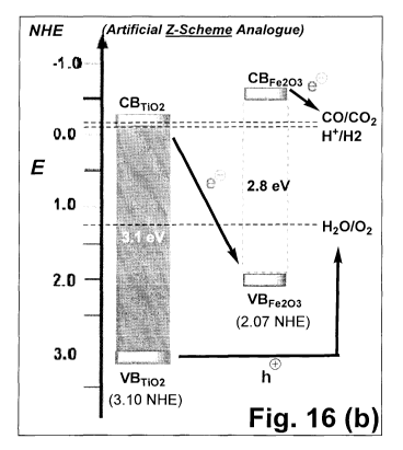
FIGS. 16A and 16B show the pairing Fe203/Ti02, in both simple and Z-scheme
electronic coupling, in
which the CB of Fe203 is around -0.5 to -0.7 eV (NHE), which is higher than
the CB of TiO2 which is around -
0.15 to - 0.35 eV (NHE). Also the VB Fe203 is around 2.07 eV (NHE), which is
higher than the VB of TiO2
around 3.10 eV (NHE). The difference between the VB and CB is the Eg, in this
example around 2.8 eV for
Fe203 and around 3.1 eV for TiO2.
FIGS. 17A-17C show the pairing Fe203/Cu20, in both simple and Z-scheme
electronic coupling. In
this example, the CB of Fe203 is around -0.5 to -0.7 eV (NHE), which is lower
than the CB of Cu20 at around
- 0.9 to 1.1 eV (NHE). Also the VB of Fe203 is around 2.07 eV (NHE), which is
lower than the VB of Cu20
which is around 1.2 to 1.4 eV (NHE). In this case, the Eg is about 2.2 eV for
Cu20.
FIGS. 18A-18C show the pairing CuO/Ti02, in both simple and Z-scheme
electronic coupling. In this
example, the CB of TiO2 is around - 0.15 to - 0.35 eV (NHE), which is lower
than the CB of CuO, at around -
8
CA 02812031 2013-03-08
WO 2012/031357 PCT/CA2011/001022
DOCSTOR:2254221 \2
0.7 eV (NHE). Also, the VB of TiO2 around 3.10 eV (NHE) is lower than the VB
of CuO, at around 1.2 eV
(NHE). The Eg for CuO is about 1.5 eV.
FIGS. 19A and 19B show the pairing SiC/Cu20, in both simple and Z-scheme
electronic coupling. In
this example, the CB of Cu20 is around - 0.9 to 1.1 eV (NHE), which is lower
than the CB of SiC at around -
2.0 eV (NHE). Also the VB of Cu20 is around 1.2 to 1.4 eV (NHE), which is
lower than the VB of SiC which
is around 0.6 eV (NHE). In this case, the electronic Eg is about 2.2 eV for
Cu20 and about 2.5 eV for SiC.
In order to photoreact with light in the visible wavelength range (e.g.,
sunlight), lower Eg values are
preferred. For example, constituents such as CuO (Eg = about 1.5 eV), Cu20 (Eg
= about 2.2 eV), SiC (Eg =
about 2.5 eV) and Fe203 (Eg about 2.8 eV) may be preferred as they are better
able to absorb sunlight energy
in the visible range of light (about 400 to 800 nm).
Selected relative VB and CB energies and Eg energies of adjacent nanoparticles
of different
photoactive constituents within a single layer or between nanoparticles of
adjacent layers of different
photoactive constituents enable efficient electronic coupling between
photoactive constituents, and help to
improve vectorial charge transport and charge carrier separation processes.
These effects may be influenced by
factors such as nanoparticle layer thickness, particle size, surface area,
surface functionality, porosity,
crystallinity and/or quantum size effects, among various others.
Pairing of two high band gap materials typically results in light absorption
that is weaker in the visible
wavelengths of light, but may provide good absorption for light outside the
visible spectrum (e.g., in the UV
range, which is considered to be above 400 nm). Pairing of two low band gap
materials typically results in
light absorption that is stronger in the visible spectrum (considered to be
between 400 nm and 800 rim) and
therefore would be more applicable to photoreactions using sunlight and/or
CSP. Pairings of materials with
different band gap values can be selected in order to obtain a desired range
of absorption wavelengths. Mixing
different pairings within the same photoactive material or combining two or
more different photoactive
materials into an assembly, as described below, can widen the range of
absorption wavelengths.
In general, CB and VB levels should be paired to have one higher and one lower
to allow charge
carrier (i.e., electron and hole) separation pathways, which locate the
generated charge carriers on separate
nanoparticles. This would minimize recombination and would favor the described
redox processes. CB and VB
values, as well as pairings of constituents may be generally known in the
literature13.
It should be noted that CB and VB values found in the literature are generally
measured for bulk
semiconductor materials. These values may be slightly different when measured
for nanoparticle or thin film
forms of these materials. However, selection of the materials and pairings can
still be carried out based on the
measurements of the bulk materials. In practice, the CB, VB and Eg energies
may be typically determined by
XPS or UPS measurements on the nanoparticles.
Selection of constituent composition
Selection of the constituent photoactive nanoparticles begins with selecting
the elemental composition
of the nanoparticles. Selection can be made from the range of single, binary,
ternary, quaternary or multi-
metallic metal oxides, metal sulfides, metal silicides, metal borides, metal
nitrides, metal phosphates, metal
pnictides and metal carbides among others. The selection is largely based on
the CB, VB and Eg values of the
materials, as described above.
9
CA 02812031 2013-03-08
WO 2012/031357 PCT/CA2011/001022
DOCSTOR:2254221 \2
Selection of constituent nanoparticle size and shape
The size of the constituent nanoparticles is also important. Typically, the
size of the photoactive
constituent nanoparticle is in the range of about 3-50 rim, and is chosen to
be smaller than the thickness of the
layer in which it is incorporated, in order to maintain a relatively flat
surface at the interface between layers or
with the air or substrate. The desired size can also depend on the specific
compound. For example, it has been
found that TiO2 nanoparticles have better performance at particles sizes of
about 12-15 nm diameter while
CuO or Fe203 nanoparticles have better performance at particle sizes of about
5-8 nm diameter.
The optimum particle size for nanoparticles of each photoactive constituent
can be determined
experimentally8. Generally, it has been found that very small particles (e.g.,
2-6 run in diameter) exhibit lower
photoactivity, perhaps due to an increase of surface defects which increase
possible charge carrier
recombination pathways. Larger particles (e.g., 10-15 nm in diameter) may have
a higher degree of
crystallinity and exhibit less surface defects.
It should be noted that while the nanoparticle size can be controlled with
known synthesis methods,
other treatments during manufacture of a nanoparticle layer or multi-layer,
such as calcination, sintering and
reduction processes, can affect the final size and shape.
The size of the constituent nanoparticles plays a role in the trade-off
between high and low porosity,
discussed above. It has been found that reaction rates showed dependence on
the particle sizes in the layer. For
example, comparing TiO2 layers with large particles ( =20-25 nm), smaller
particles ( rim) and very
small particles (
nm) the preparation with particle sizes =12-15 nm showed the best photo
activity. This
was likely due to the trade-off between porosity and surface area. In these
tests, the TiO2 layer was paired with
a Fe203 layer that was kept at a constant porosity with particle sizes of
about 4-7 rim.
The sizes of the nanoparticles may be selected depending on the specific
photoactive constituent.
Different photoactive constituents may exhibit better photaoctivity for
certain different ranges of nanoparticle
sizes, which may be due to the differences in exciton diffusion length and
surface defect density for the
different photoactive constituents. The nanoparticles used in examples
disclosed herein typically have
diameters in the range of about 1 nm to about 1000 nm, more specifically about
1 rim to about 250 rim, more
specifically about 1 rim to about 50 rim, in particular about 3 rim to about
25 rim. It should be understood that
throughout this disclosure, although diameter is used to describe the size of
the nanoparticles, the nanoparticles
may not be spherical and may have any geometry as described below.
The shape of the nanoparticle can be a well-defined morphology with well-
defined crystal facets or
random in nature, or a mixture of both. For example, the nanoparticle may have
a spherical, cubic, polyhedral,
rod, wire, sheet or any other well-defined geometry. The shape of the
nanoparticle is typically controlled
during manufacture9. Typically, a higher degree of crystallinity, with a
bigger grain size, is desirable as this
may result in less surface defects on the nanoparticle and hence less chance
of electron-hole recombinations.
The nanoparticle size distribution (PSD) is usually measured as a histogram of
the population of a
particular size versus the respective size, and is typically determined by
electron microscopy or dynamic light
scattering (DLS) studies. PSD is typically controlled during manufacture.
Generally, the more equal and/or
similar the particles are in their sizes, the lower the PSD value and the
better the dispersion quality. PSD is
mostly controlled through the synthesis process9, especially by the solvent
and the reactants, surface charge
CA 02812031 2013-03-08
WO 2012/031357 PCT/CA2011/001022
DOCSTOR:2254221\2
and zeta potential.
Below is a table providing examples of different metal oxide nanoparticles
made from metal powders,
and their particles sizes as determined using scanning transmission electron
microscopy (STEM), high
resolution transmission electron microscopy (HRTEM) and powder X-ray
diffraction (PXRD) with Rietveld
refinementig'".
Metal Metal Oxide STEM Size Size range PXRD
sizest`i
precursor Compositionlai (nm)111 (mrn)ibi
Mo Mo03 3.6 0.5 2.5 - 4.1 4 - 5 (Si)
W W03 3.8 0.3 2.0 -4.7 4 -4.5 (S2)
Ni NiO 3.1 0.4 2.2 - 3.7 amorph.
Co C0304 6.4 2.7 4.5 - 8.3 amorph.
Fe Fe203 3.4 0.5 2.7 -4.5 3-3.5 (S4)
Zn Zn02(ZnO) 3.9 0.4 3.1 - 5.2 3-4.0 (S5)
Mg Mg02 (Mg0) 4.3 0.9 3.2 - 5.7 4.5-5 (S6)
Mg + Co MgCo204 21.4 5.2 12 - 27 22 4 ( S7)
Mg + Zn MgZn204 3.5 0.4 2.8 - 4.6 amorph.
Fe+Co+Mo Fe0.3Co0.7Mo04 3.1 0.5 2.3 - 4.3 2.8-3.2
(S8)
Notes for the table above: [a] stable aqueous acidic 11202 dispersion; [b]
average particle size ranges
as determined using HRTEM and Cryo-STEM measurements; and [c] particle sizes
as determined using
PXRD Rietveld refinement.
The following table provides some example metal oxide particle sizes observed
from STEM and
XRPD measurements, as well as Brunauer Emmett Teller (BET) surface area
measurements. An alcoholic
solvent was used in the synthesis of these nanoparticles.
Metal Oxide Solvent or Solvent Size (nm) Size (nm)
BET (m2/g)tcl
Nanoparticle mixture (STEM) Ial (XRPD)Ibi
ZnO Methanol 3 - 5 3.9 0.4 150.709
ZnO Ethanol 6 - 12 10 1.7 98.368
ZnO iso-Propanol 17 - 45 42 8.6 29.598
(Fe203) Methanol / H20
a-Fe203 Ethanol / H20 4 - 7 4.6 0.41di 242.224
7.1 1.21'1
-Fe2O3 iso-Propanol / 1120 10 - 22 17.6 3 192.343
Fe203 tert-Butanol / H20 12 - 25 17.9 61d1
115.712
19.3 911)
Fe203 n-Propanol / H20 15 - 47 37.4 9td1 56.362
19.3 611
Notes for the table above: [a] STEM images were obtained using a Hitachi HD-
2000 in the Z-contrast
mode at an accelerating voltage of 200 kV and an emission current of 30-50 A;
[b] The crystal phase and
11
CA 02812031 2013-03-08
WO 2012/031357 PCT/CA2011/001022
DOCSTOR:2254221 \2
particle size was analyzed by X-ray diffraction (XRD). The Rietveld refinement
was carried out with Bruker
AXS general profile fitting software TopasTm; [c] Physisorption measurement of
40 points
adsorption/desorption isotherms, multi point (5 points) BET method was used to
determine the surface area
(g/m2); [d] Hematite phase; [e] Goethite phase; and [f] Maghematite phase.
Generally, particle size can be determined by XPRD from Rietfeld refinement
calculation or from
STEM, transmission electron microscopy (TEM) and/or HRTEM measurements.
The PSD (also referred as particle distribution (PD)) of various examples are
provided below:
For Mo03 in acidic H202/H20 - Size (nm) is 3.6 0.5, PSD or PD is 0.14;
For NiO in acidic H202/H20 - Size (urn) is 3.1 0.4, PSD or PD is 0.13;
For Fe203 in acidic H202/H20 - Size (urn) is 3.4 0.5, PSD or PD is 0.15;
For MgZn204 in acidic H202/H20 - Size (urn) is 3.5 0.4, PSD or PD is 0.11;
For ZnO in Methanol - Size (nm) is 3.9 0.4, PSD or PD is 0.1;
For ZnO in Ethanol - Size (nm) is 10 1.7, PSD or PD is 0.17;
For ZnO in Ethanol - Size (nm) is 42 8.6, PSD or PD is 0.20;
For a-Fe203 in iso-Propanol / H20 - Size (nm) is 17.6 3, PSD or PD is 0.17
The PSD or PD values listed above were obtained by division of the standard
deviation ( X) through
the average number A e.g. (ZnO in Ethanol - Size (urn) is 10 1.7, PSD or PD
is 0.17, where A is 10 and Xis
1.7, therefore the PSD or PD number results in 0.17).
PSD values typically range between about 0.10 and 0.50. A good PSD value would
be considered to
fall in the range between about 0.10 and 0.35. In the examples discussed
herein, most of the colloidal
dispersions exhibit PSD values ranging from 1.12 to 0.44.
Optical transparency of the nanoparticle layer is important for good light
penetration into the layer
with minimal light scattering loss effects. High optical transparency is
obtained when the nanoparticle
constituents are smaller than the wavelength of light, since this results in
less light scattering off the
nanoparticles. The size of the nanoparticle also affects the values of valence
band and conduction band
energies, as well as the electronic band gap. It has been found in the
examples described herein that smaller
particle sizes result in larger Eg values, and higher VB and CB values,
compared to the values measured from
bulk reference materials, due to quantum size effects. However, as noted
above, selection of constituents can
still be carried out based on those values measured from bulk materials.
The surface area of the nanoparticles is another characteristic to be
controlled. Typically, smaller
nanoparticles have larger surface to volume (SN) ratio. This ratio can be
measured by gas adsorption
isotherms1 . The SN ratio plays an important role in nanoparticle surface
chemical reactions. The larger this
ratio, the higher the number of surface active sites accessible to react with
reactants adsorbed on the
nanoparticle surface. Furthermore, SN ratios can be in general estimated from
plots of percentage of surface-
atoms of a nanoparticle as a function of the size/diameter of the
nanoparticle. This is illustrated in the table
below:
12
CA 02812031 2013-03-08
WO 2012/031357 PCT/CA2011/001022
DOCSTOR:2254221\2
Diameter S (Surface) V(Volume)
1 nm 13 1
2 nm 9 1
nm 1 1
nm 3 7
rim 1 4
60 nm 1 9
100 nm 1 20
For example, for nanoparticles having diameters in the range of about 1 nm tol
00 nm, SN ratios will
be in the range of about 13/1 (for 1 nm) up to 1/20 (for 100 nm).
It is usually desirable to have a higher SN ratio. Typically, SN values range
between about 1 and 7.
5 A good SN value may be considered to lie in the range of about 5 to 7.
The SN ratio may be controlled
through control of the particle sizes and porosity of the nanoparticle layer.
Selection of constituent degree of crystallinity
The degree of crystallinity of the constituent nanoparticles is another
characteristic that can be
controlled. Crystallinity can range from 100% amorphous (i.e., a completely
random arrangement of
10 constituent atoms) to 100% crystalline (i.e., a completely periodic
arrangement of constituent atoms in a 1D,
2D or 3D lattice or crystal structure) and arrangements in between (e.g., semi-
crystalline structures). This
characteristic is typically difficult to quantify at the nanoscale and is
usually done by high resolution electron
microscopy (HRTEM), selected area electron diffraction (SAED) and powder X-ray
diffraction (PXRD).
A good degree of crystallinity is about 95-100%, as determined from the
measured diffraction pattern.
15 Higher crystallinity, which is typically exhibited by larger particles,
may play a role in better charge separation
properties and higher photoactivity, perhaps by reducing surface defects
thereby reducing the chances of
electron-hole recombination. The degree of crystallinity is typically
controlled during manufacture, in
particular especially calcination conditions, since it has been found that
calcination at higher temperatures
generally result in to higher crystallinity. All nanoparticles of the same
constituent should exhibit the same
20 crystal structure and have similar degrees of crystallinity. Methods for
controlling crystallinity and measuring
crystallinity are generally knowni 1.
Selection of constituent surface charge
The surface charge of the constituent nanoparticle plays a role in
manufacturing a film containing the
nanoparticle. The surface charge is typically quantified by measuring the zeta
potential. The surface charge on
a nanoparticle can be positive, negative or zero. The surface charge is also
controlled by pH and ionic strength
of solvent in which the nanoparticle is dispersed. The isoelectric point is
defined as the point of zero surface
charge. Methods for controlling surface charge and its effects are generally
known12.
In the examples disclosed herein, the surface charge is generally controlled
by the amount of
protonated or de-protonated surfaces species. For example, a Fe203/Et0H
dispersion at pH = 2.26 resulted in a
positive zeta-potential of 20.1 1.1 mV, and a ZnO/Et0H dispersion at pH =
7.16 resulted in a positive zeta
potential of 31.5 0.4 mV18.
The surface charge affects the colloidal forces between nanoparticles in a
colloidal suspension since it
determines the repulsive electrical double layer (EDL) and attractive Van der
Waals (VDW) forces between
13
CA 02812031 2013-03-08
WO 2012/031357 PCT/CA2011/001022
DOCSTOR:2254221 \2
nanoparticles suspended in the solvent. The balance of EDL and VDW forces
controls the colloidal stability of
the nanoparticles in the suspension.
Colloidal stability means that the nanoparticles do not agglomerate and do not
flocculate or precipitate
from the solvent. The quality of a nanoparticle film depends on the colloidal
stability of the colloidal
dispersion and hence the colloidal surface charge. During manufacturing, an
optically transparent nanoparticle
layer of controlled porosity and thickness is obtained by evaporation induced
self assembly (EISA) through
spin-coating if the nanoparticle dispersion in the chosen solvent is
colloidally stable and does not flocculate
during the film forming process.
Porosity of a manufactured nanoparticle layer, for example as high as 30-50%
or 10-90% by volume,
depends on the void spaces that form as the nanoparticles try to pack as
efficiently as possible in the self-
assembly process, which is driven by the balance of EDL and VDW forces between
the nanoparticles. As
explained above, a controlled degree of porosity is desirable to facilitate a
balance between gas permeability
and availability of reaction sites.
Selection of constituent pairings
Photoreactions occur between pairings of two different photoactive
constituents. The selection of
these pairings is based on several characteristics.
The physical size, VB and CB energies, electronic band gap energy and
composition of the
photoactive constituent nanoparticles at least partly determine the optical
transparency, surface area, porosity,
gas diffusion and/or permeability behaviors of the photoactive material. These
characteristics of the
photoactive constituents also affect photoactivity and selectivity towards the
generation of fuels, in particular
methane and methanol (which may be produced in response to different
wavelength ranges of incident light).
By "selectivity" towards generation of fuels, it is meant that the reaction
preferentially produces a
certain product, in this disclosure typically CH4 or CH3OH. This selectivity
is based on properties such as the
specific photoactive constituents as well the specific reaction conditions.
For example, by using preferentially
specific constituents such as CuO, Cu20 or Cu metal in the photoactive
material, the material may exhibit
higher selectivity towards generation of CH3OH.
Examples of selectivity of some photoactive constituents are shown in the
table below:
Constituents Main photoreaction products
Cu/Fe* co-doped TiO2 Methane (CH4)
Pt/TiO2 or Ru/Itu02/Ti02 Methane (CH4)
Cu/ZnO/Si02 Methanol (CH3OH)
NiO/InTa04 Methanol (CH3OH)
Monoclinic BiVO4 Ethanol (C2H5OH)
* Cu(0.25 wt%)/Fe(0.25 wt%)
The constituent pairing should also be selected such that the total light
absorption is over as broad a
wavelength range as possible. This photoelectric coupling is generally
described in the literature". For
example, ZnO/TiO2 may be considered a poor pairing since both semiconductors
absorb mostly in the UV-part
of the sunlight spectrum. A better pairing would be Fe203/Ti02 where at least
one constituent, specifically
Fe203, possesses a stronger absorption in the visible range (400 nm to 800
nm). An even better example would
be Fe203/CuO or Fe203/Cu20 because both constituents absorb a broad wavelength
of light, including the
visible range. Another good combination would be SiC/CuO where SiC absorbs in
the near infrared range and
14
CA 02812031 2013-03-08
WO 2012/031357 PCT/CA2011/001022
DOCSTOR:2254221\2
CuO absorbs in the visible range, thereby combining to provide light
absorption in the near infrared and visible
wavelength ranges.
Where the multi-layered photoactive material is arranged as a photonic
crystal, the constituents may
be selected to have large refractive index contrast (RIC) values, in order to
achieve strong slow photon effects,
as will be discussed below. A large RIC may be considered to be in the range
of about 0.5 to 0.75 or 0.5 to 1Ø
RI values for different bulk materials are generally known and can be found in
various references and
databases". In general, RI is affected by the choice of constituent and degree
of porosity and/or thickness of
the resulting nanoparticle layer, examples of which will be described below.
Typically, the RIC between the layers of a multi-layered photoactive material
is a function of the
characteristics of the selected photoactive constituents and/or the porosity
of the individual layers.
Electronic coupling between more photosensitive (i.e., narrower electronic
band gap) and less
photosensitive (i.e., wider electronic band gap) constituents may also have
beneficial effects on the photoactive
performance of the photoactive materials. Photosentivity of a material may be
determined by measuring the
material's absorption of different wavelength ranges of light, particularly in
the visible spectrum (i.e., about
400 to 700 nm). A less photosensitive material is considered to have
absorption below 400 nm (e.g. ZnO or
TiO2 nanoparticles), while a more photosensitive material is considered to
have absorption within the visible
spectrum (e.g., CuO nanoparticles, which have absorption from about 700 to 350
nm or Fe203 nanoparticles,
which have absorption from about 550 to 350 nm).
These pairings may be present as a mixture of the two constituents within a
single-layer photoactive
material; or may be present as separate layers of each constituent in a multi-
layer photoactive material.
Example photoactive constituents
Examples of photoactive constituents and their pairings that are suitable for
a photoactive material are
now described. These pairings are selected based on known electronic coupling
between the photoactive
constituents, as discussed above.
Example pairings include: Ti02/W03, Ti02/ZnO, Ti02/CdSe, Ti02/CuO, Ti02/NiO,
Ti02/ Fe203,
W03/ Fe203.
Examples of coupling between more photosensitive and less photosensitive
constituents can be found
in the following layer pairs:
Ti02/Sn02, Ti02/ ATO NiO/ ATO -Sn02:Sb Ti02/Si02, Ti02/A1203 or
TiO2/Z102.
To help improve the absorption of photons for photoactive reactions, a
combination of optical
absorption and electronic band properties may be selected. For instance, by
combining relatively high
electronic band gap metal oxide nanoparticles (e.g. Ti02, ZnO, Sn02, ATO .-
Sn02:Sb or mixed composition
thereof) with relatively low electronic band gap metal oxide nanoparticles
(e.g., Fe203, Co203, CuO, Cu20,
Ru02 or mixed composition thereof), the optical absorption properties of the
photoactive material can be
selected to occur at the energy of the lower electronic band gap constituent
due to the convolution of the
optical absorption properties of each layer, as discussed above.
Other examples of photoactive constituents and pairings are described in
detail below. These
photoactive constituent pairs can be used in the single-layer photoactive
material and/or the multi-layered
photoactive material, as will be discussed below.
CA 02812031 2013-03-08
WO 2012/031357 PCT/CA2011/001022
DOCSTOR:2254221
Example I - CuO/Ti02 or Cu20/Ti02pairs
Through electronic band gap engineering of the energy levels of nanoparticle
constituents in a
photoactive material, as described above, vectorial charge transport and
charge carrier separation between the
different photoactive constituents may be selected to favor a hole-rich layer
and an electron-rich layer.
An example are the CuO/TiO2 and Cu20/Ti02 pairs, which may be arranged as
alternating layers of
CuO/Ti02 or Cu20/Ti02 or as mixed CuO/Cu20-Ti02 layers, in a multi-layered
photoactive material. These
constituents may also be mixed together in a single-layer photoactive
material. These constituent pairs may be
arranged to achieve an optimal band-gap alignment.
In this example, the action of light may be described as follows:
TiO2 + CuO and/or Cu20 + by -0 CuO and/or Cu2Oecd + TiO2hv8+
In this example, the resulting CuO and Cu20 electron-rich layers may
participate in CO2 reduction
while the resulting TiO2 hole-rich layers may concurrently enable 1120
oxidation. Reactions of this type may
occur within or between layers of adjacent electronically-coupled nanoparticle
layers in a multi-layered
photoactive material; or within a single-layer of mixed nanoparticles in a
single-layer photoactive material.
FIGS. 3A-3B illustrate electronic band gap engineering of the example CuO/Ti02
pairing. It should be
understood that although the redox reaction is illustrated here and in later
examples with respect to a multi-
layered photoactive material made of layers of different photoactive
constituents, such a reaction can also take
place within a single-layer photoactive material containing a mixture of at
least two different photoactive
constituents.
FIG. 3A-B illustrates the formation of charge carriers and the redox of CO2
and H20 that is enabled in
a photoactive material having nanoparticle CuO/Ti02 layers. In the example
shown, the CuO layers 301
alternate with TiO2 layers 302. The CuO layers 301 undergo
activation/reduction of CO2 while the TiO2 layers
302 undergo oxidation of water, resulting in the reduction and activation of
CO2 or the generation of HI
The photoreactions carried out in the photoactive material include
simultaneous oxidation and
reduction, such as exemplified by the reactions CO2 + H20 and CO2 + 112, in
particular the concurrent
oxidative splitting of water and reduction of CO2 as illustrated below:
CO2 +4112 CH4 (g) +21120 and
CO2 + 2H20 -0 CH3OH(1) + 3/202
The product water may be re-used and/or recycled or split in situ in
additional reactions with the hole-
rich and electron-rich species, as shown in the example below.
The following equations illustrate reactions that may take place within a
photoactive material:
(electron-rich reaction) CO2+ CuO and/or Cu2Oecs- - (COD*
2H+ + CuO and/or Cu2Oec13" -> 112 or (211)
(hole-rich reaction) 1120+ TiO2hvB+ =OH + H+
OH + H+ + TiO2hvB+ -* Y2 02 (g) + 2 H+
(CO2)* +211+ TiO2hv8 -> CO +1120
(CO)* + 6H + TiO2hvB+ CH4 + H2O
(CO2-)* +811+ TiO2hvB+ CH4 +21120
where * indicates an activated state of a compound. The redox processes for
the photon-driven
16
CA 02812031 2013-03-08
WO 2012/031357 PCT/CA2011/001022
DOCSTOR:2254221
generation of adjacent electron- and hole-rich species are designed, through
electronic band energy and
electronic band gap engineering, as described above, to enable the concurrent
reduction and oxidation of CO2
and H20 respectively. These processes may occur in a multi-layered photoactive
material as well as in a
single-layer photoactive material.
Example 2 - Ti02/W03 pairs
In this example, the photoactive constituents include photoactive TiO2
nanoparticles and photoactive
W03 nanoparticles. In this example, similar to example 1 above, the action of
light is described by the
reduction of CO2 and oxidation of H20 within a photoactive material, whether
single-layer or multi-layered,
according to the following reaction equations:
TiO2 + WO3 + hi) WO3ecd + TiO2hvs+
(electron-rich reaction) CO2 + WO3ecd (COD*
2H+ + WO3eC13- "-* H2 or (2H)
(hole-rich reaction) H20 + TiO2hva =OH + H
OH + H+ + TiO2hv9+ 1/2 02 (g) +2 H+
(CO2-)*+ 2H + TiO2hvs+ CO + H20
(CO)* + 6H + TiO2hve+ -> CH4 + H20
(CO2)* + 8H + TiO2hvs+ -> CH4 +2 H20
where * indicates an activated state of a compound. The redox processes for
the photon-driven
generation of adjacent electron- and hole-rich species are designed, through
electronic band energy and
electronic band gap engineering, as described above, to enable the concurrent
reduction and oxidation of CO2
and H20 respectively. These processes may occur in a multi-layered photoactive
material as well as in a
single-layer photoactive material.
Example 3- ce-Fe203/Ti02 pairs
In this example, the photoactive constituents include photoactive TiO2
nanoparticles and photoactive
a-Fe2O3 (hematite) nanoparticles. In this example, similar to example 1 above,
the action of light is described
by the reduction of CO2 and oxidation of H2O within a photoactive material,
whether single-layer or multi-
layered, according to the following reaction equations:
TiO2 + a-Fe2O3 + a-Fe203ecd + TiO2hvB+
(electron-rich reaction) CO2+ a-Fe203eca. (Clai)*
2H+ + a-Fe203eC13- -> H2 or (2H)
(hole-rich reaction) H2O + TiO2hv B+ = OH + H
OH + H+ + TiO2hv8+ -> 1/2 02 (g) +2 H+
(CO2-)*+ 2H + TiO2hvo+ CO + H2O
(CO)* + 6H + TiO2hvB -> CH4 + H2O
(CO2)* + 8H + TiO2hv8+ -> CH4 +2 H20
where * indicates an activated state of a compound. The redox processes for
the photon-driven
generation of adjacent electron- and hole-rich species are designed, through
electronic band energy and
electronic band gap engineering, as described above, to enable the concurrent
reduction and oxidation of CO2
and H2O respectively. These processes may occur in a multi-layered photoactive
material as well as in a
17
CA 02812031 2013-03-08
WO 2012/031357 PCT/CA2011/001022
DOCSTOR:2254221\2
single-layer photoactive material.
FIG. 4A-B illustrates the formation of charge carriers and the redox of CO2
and H20 that is enabled in
a photoactive material having nanoparticle Fe203/Ti02 layers. In the example
shown, the TiO2 layers 402
alternate with Fe203 layers 401. The Fe203 layers 401 undergo
activation/reduction of CO2 while the TiO2
layers 402 undergo oxidation of H20, resulting in the reduction and activation
of CO2 or the generation of 112.
Example 4¨ Cu(Cu20)/a-Fe203 pairs
In this example, the photoactive constituents include photoactive Cu(CuO) and
Fe2O3 nanoparticles.
These constituents may be mixed together in a single-layer photoactive
material, or as separate layers in a
multi-layered photoactive material.
Similar to example 1 above, electronic coupling between different photoactive
nanoparticles leads to
an improved charge carrier production and separation of electron-hole pairs,
and the copper nanoparticles
enables improved photoactive activity.
Additionally, in this example, the copper nanoparticles may give rise to
plasmonic resonance, which
enhances the absorption of light and the photoactivity of a photoactive
material incorporating Cu(Cu20)/a-
Fe2O3. This will be described in greater detail below.
Interfaces between the electron-rich Cu and hole-rich Fe203 nanoparticles may
also function as a
Schottky barrier, which suppresses electron-hole recombination processes.
A Schottky barrier is defined as the interface, boundary or electronic
interface between a metal and a
semiconductor . The Schottky barrier serves to suppress electron-hole
recombination processes, as the
electron gets trapped within the metal (e.g. Cu, Ag, Au or Pt) and the hole
remains on the more acidic metal
oxide (e.g. Fe203, h02, W03, among others).
In this example, similar to example 1 above, the action of light is described
by the reduction of CO2
and oxidation of 1120 that may take place within a photoactive material,
whether single-layer or multi-layered,
according to the following reaction equations:
Cu(CuO) + Fe203 + hp Cu(CuO)eca-
+ _ F
e2_3hva+
(electron-rich reaction) CO2+ Cu(CuO)ecB- (CO2
2H+ + Cu(CuO)ear H2 or (211)
(hole-rich reaction) 1120 + Fe203hv8+ =OH + H
OH + H+ + Fe203hvB+ Y2 02 (g) 2 H+
(CO2-)*+ 2H + Fe203hvB+ ¨> CO +1120
(CO)* + 611+ Fe203hvB+ CH4 + H20
(CO2)* +611+ Fe203hvB+ CH3OH +1120
where * indicates an activated state of a compound. The redox processes for
the photon-driven
generation of adjacent electron- and hole-rich species are designed, through
electronic band energy and
electronic band gap engineering, as described above, to enable the concurrent
reduction and oxidation of CO2
and H2O respectively. These processes may occur in a multi-layered photoactive
material as well as in a
single-layer photoactive material.
18
CA 02812031 2013-03-08
WO 2012/031357 PCT/CA2011/001022
DOCSTOR:2254221\2
Example 5- Cu20/SiC pairs
In this example, the photoactive constituents include photoactive Cu20
nanoparticles and photoactive
SiC nanoparticles. In this example, similar to example 1 above, the action of
light is described by the reduction
of CO2 and oxidation of 1120 that may take place within a photoactive
material, whether single-layer or multi-
layered, according to the following reaction equations:
SiC + Cu20 + SiCecd + Cu20hvB+
(electron-rich reaction) CO2+ SiCeci; --0 (CO2-)*
2H+ + H2 or (2H)
(hole-rich reaction) H20 + Cu2011ivB+ =OH + H
OH + H+ + Cu2OhvB+ -> IA 02 (g) + 2 H+
(CO2-)*+ 2H + Cu20hvB+-0 CO + H20
(CO)* + 6H+ Cu201IvB+ CH4 + H20
(CO2-)* + 8H + Cu2OhvB+ CH, +21120
where * indicates an activated state of a compound. The redox processes for
the photon-driven
generation of adjacent electron- and hole-rich species are designed, through
electronic band energy and
electronic band gap engineering, as described above, to enable the concurrent
reduction and oxidation of CO2
and 1120 respectively. These processes may occur in a multi-layered
photoactive material as well as in a
single-layer photoactive material.
Other examples
Other example photoactive constituents are described below. These are
selectable from known earth-
abundant, easy to synthesize, colloidally stable, inexpensive and/or non-toxic
metal oxides. Such metal oxides
include, for example, constituent pairs having the general stoichiometric
formulation: M3n0y/M260õ; Min0y-
m21103,843.0z; minoy_m2.0y/m3noz_manoz; mniioyfmnnu-z
(where M is a suitable metal and n, x, y, z are
integers). The constituents may also include mixed compositions, solid-
solution, combinations with other
semiconductor materials, as well as non-stoichiometTic compositions (e.g. MOõ
wherein 0.1 and/or
combinations thereof. It should be understood that in the present disclosure,
the term non-stoichiometric is
intended to include sub-stoichiometric compositions.
In particular, suitable photoactive constituent pairs include:
Fe2O3/TiO2; Fe2O3/W03; ZnO/Ti02; ZnO/W03; CuO/Fe203; CuO-ZnO/Fe203; CuO/Ti02;
CuO/W03;
CuO-ZnO/Ti02; CuO-ZnO/W03; CuO-Fe203/Zn0; CoO/Ti02; Co304/W03; Co304-ZnO/Ti02;
Co304-
Fe203/W03; CuO-Co304/Fe203; Ce02/Fe203; Ce02/Ti02; Ce02/W03; Ce02-NiO/Ti02;
CoO-Ce02/W03;
ATO/Fe203; Fe203/NiO-Co304; Cu20-ATO/Fe203; NiO/Fe2O3; NiO/Ti02; SiC/Cu0;
ITO/W03; Cu20/Fe2O3;
Cu20/TiO2; ATO-CuO/SiC; NiO-Fe203/Cu20; SiC/Cu20; SiC-Cu20/Fe203; Ti02/W03;
Fe203-CuO/Ni0;
Fe2O3-NiO/Cu0; ZnFe204/Ti02; MgCo204/W03; Ti02/ATO; Fe203-CuO/ATO; BiVO4/Ni0;
Bi2W06/Cu20;
ITO-Cu20/W03 and NiW04/Fe203-Cu20.
Further, the following species are known to be suitable for photoactive
constituents":
I) Simple Metal-Oxides e.g.: in all known modifications and polymorphs e.g. a-
; (3-; 1,-; 5- as well as all
possible non-stoichiometric compositions and/or combinations thereof MOõ
wherein 0.1
= A1203, A100H, and all known modifications and polymorphs e.g. a-; 13-; 1,-
; 5-
19
CA 02812031 2013-03-08
WO 2012/031357 PCT/CA2011/001022
DOCSTOR:2254221 \2
= FeO, Fe0(OH), Fe(OH)3, Fe203, Fe304 and all known modifications and
polymorphs e.g. a-; (3-;
= TiO2 (rutile, anatase & brookite-phase); Sn02, Ti203 and all known
modifications and polymorphs e.g. a-;
l3-; 7-; 6-
= MgO, CaO, Sr0, BaO, Co0 and all known modifications and polymorphs e.g. a-
; (3-; -y-; 6-
= CuO, Cu20, NiO, ZnO, Be0 and all known modifications and polymorphs e.g.
a-; 0-; '14; 45-
= W03, Mo03 and all known modifications and polymorphs e.g. a-; 13-; 1,-; 6-
= Si02, B203, Ge02,
Mn02 and all known modifications and polymorphs e.g. a-; ry-; 6-
= Ta205, Nb205,
V205, Co304 and all known modifications and polymorphs e.g. a-; 14; 6-
= Ga203, Cr203, Mn203, V203, Nb203 and all known modifications and
polymorphs a-; 13-; 7-; 6-
= La203, Bi203, Sb205 and all known modifications and polymorphs e.g. a-; 0-
; '14; .5-
= Sn02, Zr02, Ce02, V02, Th02, Te02 and all known modifications and
polymorphs a-; 13-; 7-;
= Ag20, Pd0, Ru02, Au20, 1r02, Re207 and all known modifications and
polymorphs a-; 0-; 14; (5-
= P205, P4010 in all known modifications and polymorphs aL; 0-; 7-;
= Transparent conductive metal oxides (TC0s), e.g. ITO -==In205:Sn (Indium
Tin Oxide), ATO Sn02:Sb
(Antimony Tin Oxide), FTO (Flourine Tin Oxide), ZTO --Sn02:Zn (Zinc Tin
Oxide), IZO
In205:Zn (Indium Zinc Oxide) as well as various mixtures thereof and with any
other photoactive
semiconductor materials, including solid solutions, core@shell e.g. MOs@TCO
structures in all known
and possible modifications, non-stoichiometric compositions and/or
combinations thereof and/or different
doping levels and polymorphs a-; (-; -y-; 6-.
= Porous metallic films, resulting from reduction of metal oxide
components, e.g. porous Au, Ag, Cu, p-Si,
porous Si, crystalline Si, amorphous Si, porous Si nanowires'5, as well as
various mixtures thereof and
with any other photoactive materials, including various alloys M1-M2 and
core@shell e.g. M1@M2.
H) Mixed Metal-Oxides e.g.: in all known modifications and polymorphs a-; ft-;
7-; 6- as well as all possible
non-stoichiometric compositions (e.g., M'M20õ wherein 0.1 and/or
combinations thereof
= Rock-salt solid solutions e.g. (Mg1.,Ca.0) (wherein 0.1
= Cal,BixVõMo104 solid solutions (wherein 0.1
= Na1,LaxTa3,Co,(03 solid solutions (wherein 0.1 :5_x
= (AgNb03)1(NaNb03)õ solid solutions (wherein 0.1
= Corundum solid solutions e.g. (FeCr)203
= Spinels AB204 e.g. (MgA1204)
= Ilmenites ABO3 e.g. (FeTiO3)
= Perovskites ABO3 e.g. (CaTiO3)
= Olivins A2B04 e.g. (Mg2SiO4)
= Granates A(H)3B(III)2Si3012 e.g. (Fe3Al2Si3012)
= Gallium and Zinc nitrogen oxide
(Gai,ZnANI-x0.) (wherein 0.1 =1)
= Ti-silicates (TiO2 in Si02)
= Aluminas and Silicated Aluminas (Si-A1203)
= Polyoxymetallates in general (e.g., [EW10036]12 or [EMo12041-12)
CA 02812031 2013-03-08
WO 2012/031357 PCT/CA2011/001022
DOCSTOR:225 4221 \2
III) Multicomponent Mixed Metal-Oxides (which may be photoactive for visible
light irradiation): e.g. in all
known modifications and polymorphs a-; 13-; 1,-; 6- as well as all possible
non-stoichiometric compositions
and/or combinations thereof e.g. MaMbMc0,, wherein 0 ".2(
= BiVO4, Vi2W06, Bi2M0065 NiWai, II1VO4, Caiil04, InNb04, Pb3Nb4013,BaBi03,
CaBi204, AgA102,
Ag2Cr04, AgCr02, AgInW208, PbBi2Nb209, Zn2.5VMo08, In12NiCr2Ti10042, Ini-
xNixTa04, InTa04,
SrTiO3, La2Ti207, LaTi05, Sr3Ti207, BaTi409, PbTiO3, or M2Ti6012 (M = Na, K,
Rb), Fe0.3030.7M004,
K4Nb6017, KCa2Nb3010, KNb308, KTiNb05, M2BiNb07 (M = Ca, In, Ln), H2SrTa207,
NaTa03, LnTa04,
M0.5Nb0.503 (M=Ca, Sr, Ba), K4Ce2Nb10030, PbBi2Nb209, In6NiTi6022,
In3CrTi2010, In12NiCr2Ti10042,
Nb2Zr201.2N2, Nb2Zr6017, or generally:
= MMb80y or Mni.õMmx0y ; Mai,Mb8McOy
mal_mmbamcbmdcmnmoy
IV) Metal carbides in general, in all known modifications and polymorphs a-; 0-
; 1,-; 15- as well as all possible
non-stoichiometric compositions and/or combinations thereof (e.g. Ta4C3,
Nb4C3, Mo3C2, Fe3C, SiC);
V) Metal nitrides in general, in all known modifications and polymorphs a-; (3-
; 7-; 6- as well as all possible
non-stoichiometric compositions and/or combinations thereof (e.g. Ta3N5, TiN,
Si3N4). This may include
metal-(oxy)nitrides in general in all known modifications and polymorphs a-;
15-; 1,-; 6- as well as all possible
non-stoichiometric compositions and/or combinations thereof (e.g. GaN, Ge3N4,
GelN14, Ta0N, Zr202N2,
Y2Ta205N2)
VI) Metal borates and borides in general, in all known modifications and
polymorphs a-; )3-; ry-; 5- as well as
all possible non-stoichiometric compositions and/or combinations thereof (e.g.
Ni(B02)2 x H20, Co(B02)2,
YB6, REA1B14);
VII) Chalcogenides in general, e.g. Metal sulfides in all known modifications
and polymorphs a-; #-; ry-; 8- as
well as all possible non-stoichiometric compositions and/or combinations
thereof (e.g. Ag2S, ZnS, MoS2, WS2,
CdS, AgInS2, PeS2, Znin2S4);
VIII) Metal chalcogenides in general, in all known modifications and
polymorphs a-; )3-; ry-; 8- as well as all
possible non-stoichiometric compositions and/or combinations thereof (e.g.,
CdSe; ZnSe, CIGS (Copper
indium gallium selenides);
IX) Metal phosphate, -polyphosphates and phosphides in general, in all known
modifications and polymorphs
a-; 13-; 1,-; 8- as well as all possible non-stoichiometric compositions
and/or combinations thereof (e.g.
Ag3(PO4), CO3(PO4)2, Cu2(PO4)0H, Ni3(PO4)2, Zn3(PO4)2, Zn3P2, TiP, InP, GaP)
X) Metal arsenides in general, in all known modifications and polymorphs a-; 0-
; 7-; 8- as well as all possible
non-stoichiometric compositions and/or combinations thereof (e.g. GaAs, InAs)
Note that metal nitrides, metal phosphides and metal arsenides generally fall
into the class of metal pnictides.
XI) Metal suicides in general, in all known modifications and polymorphs a-;
)3-; 1,-; 6- as well as all possible
non-stoichiometTic compositions and/or combinations thereof (e.g. NiSi, WSi2,
PtSi, TiSi2)
XII) Metal-oxy-sulfides and metal oxyhalides in general, in all known
modifications and polymorphs a-; i3-; y-
8- as well as all possible non-stoichiometric compositions and/or combinations
thereof (e.g. Bi4NbO8C1,
AgC102)
21
CA 02812031 2013-03-08
WO 2012/031357 PCT/CA2011/001022
DOCSTOR:2254221 \2
For IV) to XII) above, also all known modifications e.g. a-; (3-; 7-; (5-; E-;
n-; ff..; as well as all possible
non-stoichiometric compositions and/or combinations thereof, all known
polymorphs and/or further mixed
phases of the above, which can occur also as mixed oxy-hydroxyl species, among
various others possible
combinations.
XIII) Organic semiconductors, porous semiconductor polymers and carbon
compounds (e.g., carbon, graphite,
diamond, carbon nitride, g-C3N4 and all known modifications polymorphs a-; (3-
; y-; 8-; Ã-; n-; 0-; as well all as
possible non-stoichiometric compositions and/or combinations thereof thereof
etc.)
XIV) Up-converter nanocrystals in general in all known modifications and
polymorphs a-;(3-; 7-; (5- as well as
all possible non-stoichiometric compositions and/or combinations thereof (e.g.
NaYF4, LaF3, Y203, Gd203,
Nd203, Er203, Sm203, Gd203 and their doped or codoped systems with e.g. Er3+
and/or Yb3+).
The metal oxides used may include the simple metal oxide and all their known
modifications e.g. a-;
(3-;
(5-; c-; n-; e-; as well as all possible non-stoichiometric compositions
and/or combinations thereof. The
stoichiometric compositions may be generally denoted as MOy (where n and y are
integers), (e.g., Ti02, W03,
Sn02, ITO .In205:Sn (Indium Tin Oxide), ATO (Antimony Tin Oxide), FTO
(Flourine
Tin Oxide), ZTO E---Sn02:Zn (Zinc Tin Oxide), IZO E.--In205:Zn (Indium Zinc
Oxide), ZnO or Fe2O3 as well as
various possible mixtures thereof).
They may further include bimetallic mixed metal oxides (e.g., non-
stoichiometric compositions M.
xMb,c0 and stoichiometric compositions (MaMb)n0y, AB204, AB03), multi-metallic
and multi-component
metal oxide composites and compositions as core@shell structures M'O@M20 (e.g.
CuO@Fe203,
Cu2O@CuO, FeTiO3CuO@Cu20, NiO@Cu20), as well as heterodimeric nanoparticle
assemblies M10-M20
(e.g., NiO-CuO, CuO-Fe203, MnFe204-Cu2O). Additionally, the different metal-
oxide compounds and
compositions may be doped and co-doped with or by the following metallic and
non-metallic dopants and co-
dopants in their different occurring oxidation states e.g. Mn+, with n = 1 to
8.
- for example with the following non-metallic dopants "D": B, Si, C, S, Se, P,
As, F, N, I, that may be
generally denoted, in non-stoichiometric compositions, as M1_yDy0x wherein 0.1
5x and y 51 and all possible
non-stoichiometric compositions and/or combinations thereof.
- for example with the following metallic dopants "D": Be, Li, K, Mg, Ca, Sc,
Y, Ti, Zr, Hf, V, Nb,
Ta, Cr, Mo, W, Mn, (Tc), Re, Fe, Ru, Os, Co, Rh, Ir, Ni, Pd, Pt, Cu, Ag, Au,
Zn, Cd, (Hg), Al, Ga, In, Tl, Ge,
Sn, Pb, Sb, Bi, Te, Po, At, La, Ce, Pr, Nd, Eu, Gd, Tb, Dy, Ho, Er, Tm, Yb,
Lu, Ac, Th, Pa, U, Pu; generally
denoted, in non-stoichiometric compositions, as 1µ41Dy0õ wherein 0.1 5x and y
51 and all possible non-
stoichiometric compositions and/or combinations thereof.
The disclosed photoactive materials may also incorporate metal oxides (MO),
bimetallic mixed
metal-oxides (e.g., non- stoichiometric compositions Mai.õMb,(0 and
stoichiometric compositions (MaMb)õ0y,
AB204, AB03), multi-metallic and multi-component metal oxide composites, as
well as non-stoichiometric
compositions and/or combinations thereof.
Other examples of photoactive constituents and their pairings that may be
suitable for use in the
disclosed photoactive material are shown in the tables below (--- indicates no
pairing, xxx indicates the pairing
did not exhibit a photonic stop band):
22
CA 02812031 2013-03-08
WO 2012/031357 PCT/CA2011/001022
DOCSTOR:2254221\2
Pairings with metal oxides:
TiO2 ZnO Fe203 W03
TiO2 _ Ti02/ZnO TiO2/Fe203 TiO2/W03
ZnO ZnO/TiO2 ¨ ¨ ¨ , XXX ZnO/W03
Fe203 Fe203/Ti02 XXX ¨ ¨ ¨ Fe203/W03
W03 W03/Ti02 W03/ZnO W03/Fe203 ¨ ¨ ¨
CuO CuO/Ti02 XXX XXX CuO/W03
NiO NiO/Ti02 XXX XXX NiO/W03
Sn02 Sn02/TiO2 XXX XXX Sn02/W03
Si02 Si02/Ti02 XXX XXX Si02/W03
MgO / MgF2 MgO or MgF2 / TiO2 XXX XXX MgO or MgF2 / W03
A1203 A1203/Ti02 XXX XXX A1203/W03
ATO ATO/Ti02 XXX XXX ATO/W03
ITO ITO/Ti02 ITO/ZnO ITO/Fe203 ITO/W03
Pairings with catalytic constituents:
CuO NiO Sn02
TiO2 Ti02/CuO Ti02/Ni0 Ti02/Sn02
ZnO XXX XXX XXX
Fe203 XXX XXX XXX
W03 W03/CuO W03/NiO W03/Sn02
CuO --- XXX XXX
NiO XXX --- XXX
Sn02 XXX XXX ¨ ¨ ¨
Si02 XXX XXX XXX
MgO / MgF2 XXX XXX XXX
A1203 XXX XXX XXX
ATO XXX XXX XXX
ITO ITO/CuO ITO/NiO ITO/Sn02
Pairings with low refractive metal oxides:
S102 MgO / MgF2 A1203
TiO2 / MgO or
TiO2 Ti02/Si02 MgF2 Ti02/A1203
ZnO XXX XXX XXX
Fe203 XXX XXX XXX
W03/ MgO or
W03 W03/Si02 MgF2 W03/A1203
CuO XXX XXX XXX
NiO XXX XXX XXX
Sn02 XXX XXX XXX
Si02 ¨ ¨ ¨ XXX XXX
MgO / MgF2 XXX ¨ ¨ ¨ XXX
A1203 XXX XXX ¨ ¨ ¨ ,
ATO XXX XXX XXX
ITO/ MgO or
ITO ITO/Si02 MgF2 ITO/A1203
23
CA 02812031 2013-03-08
WO 2012/031357 PCT/CA2011/001022
DOCSTOR:2254221\2
Pairings with conductive metal oxides:
ATO ITO
TiO2 Ti02/ATO Ti02/ITO
ZnO XXX ZnO/ITO
F e2 03 XXX Fe203/ITO
W03 W03/ATO W03/ITO
CuO XXX CuO/ITO
NiO XXX NiO/ITO
Sn02 XXX Sn02/ITO
Si02 XXX Si02/ITO
MgO or MgF2
MgO / MgF2 XXX / ITO
A1203 XXX A1203 / ITO
ATO ¨ ¨ ¨ ATO/ITO
ITO ITO/ATO ¨ ¨ ¨
The photoactive constituent pairings may be pairings of simple nanoparticles,
pairings of mixed metal
oxide nanoparticles, and pairings of physically mixed nanoparticles.
Examples of simple nanoparticle pairings include: ZnO/Ti02; W03/Ti02;
Ce02/Ti02; ZrO2/TiO2;
A1203/Ti02; and pairings with metal nanoparticles such as Au, Ag, Cu, Pt and
Ru or Ru02. Examples of
mixed metal oxide nanoparticles include: ZnO-CuO/Ti02-Ru02; ZnO-Ni0M02-Mn02;
and TiO2 or Ru02-
Ti02 pairing with MO2 (where M = V, Nb, Ru, Cr or Mn). Examples of physically
mixed nanoparticles
include: ZnO:CuO/Ti02:Cr02:Ru02 and ZnO:NiO/Ti02:Mn02:Ce02.
Selection of layer properties
The nanoparticle layer is also designed to obtain a desired combination of
optical transparency,
porosity and thickness.
Optical transparency is a desirable characteristic as it enables good light
penetration throughout the
layer. This provides the maximum possible light absorption by the photoactive
constituent nanoparticles,
thereby maximizing the formation of reactive electron-hole pairs. This allows
for a greater number of CO2
reduction events and number of H2 and/or H20 oxidation events on the surface
of the photoactive
nanoparticles.
Maximizing the porosity (e.g., about 10-90%, in particular 30-50%) of the
layer also helps to promote
photo-driven redox reactions by providing as much accessible active surface
reaction sites to the reactants
(namely CO2 with H2 and/or 1120) as possible. Greater porosity allows the
reactants to diffuse into the porous
nanoparticle layer and fmd as many active surface sites on the nanoparticles
as possible, as well as allowing
reaction products to escape/diffuse out from the nanoparticle layer.
The thickness of the nanoparticle layer will determine the total surface area
and porosity of the film
and hence the number of reactant molecules that can enter the pore spaces and
participate in nanoparticle
surface reactions with generated electron-hole pairs. As well the layer
thickness also plays a role in permitting
efficient electron-hole separation and preventing electron-hole recombination.
Layer thickness
The layers of the disclosed photoactive material have layer thicknesses
selected to promote efficient
charge carrier separations and heterojunction electronic band gap coupling
between different nanoparticle
24
CA 02812031 2013-03-08
WO 2012/031357 PCT/CA2011/001022
DOCSTOR:2254221 \2
constituents. The layer thickness is on the order of nanoscale, that is, less
than a micron thick. The thickness is
selected in order to maximize charge carrier separation efficiencies and to
suppress recombination of generated
electron-hole pairs and help improve the photoactivity of the disclosed
photoactive material.
The general efficiency of the multi-layered photoactive material in capturing
light to drive a
photoactive reaction is dependent on the thicknesses of the constituent layers
in the layered material.
Typically, there is an optimal thickness for each constituent layer. These
layer thicknesses affect the efficiency
of separating the generated electron-hole pairs within and between the layers.
For optimal efficiency of
electron-hole separation in multi-layered photoactive materials, the layer
thicknesses should be selected to be
equal to, slightly larger (e.g., 2-20 nm), or slightly smaller (e.g., 2-20
nm) than the exciton (i.e., electron-
hole pair) diffusion lengths. The diffusion lengths depend upon the choice of
the photoactive constituents (e.g.
diffusions length for Fe203=--20-25 nm and TiO2 27-30 nm). These diffusion
lengths and optimal layer
thicknesses are commonly known.16
Generally, the exciton diffusion length is dependent on exciton mobility and
exciton lifetime. Exciton
mobility depends on exciton diffusion lengths (e.g., the thickness of a thin
film containing the exciton).
Exciton lifetimes can be extended through the use of triplet semiconductor
materials, which often posses much
longer exciton lifetimes compared with singlet semiconductor materials.
Where the photoactive material is a single-layer arrangement of mixed
constituents, the efficiency of
separating the electron-hole pairs is affected by the distance between two
different photoactive constituents.
This distance is largely dependent on the size of the constituent
nanoparticles, since the greatest distance
between electron-hole pairs would be the distance between the centers of two
different adjacent constituent
nanoparticles. Similar to the determination of layer thickness described
above, the nanoparticle size should be
selected to be equal to, slightly larger (e.g., 2-20 tun), or slightly
smaller (e.g., 2-20 nm) than the exciton
diffusion lengths of the photoactive constituent nanoparticles.
Judiciously selected layer thicknesses and nanoparticle sizes results in
improved gas-diffusion
processes and flow-through properties, as well as contact and residence times
for gas-solid photoreactions in
the photoactive material.
The layers may have thicknesses in the range of about 1 tun to about 1000 nm.
It has also been shown,
both from literature16 and from studies discussed herein that a thinner layer
(e.g., about 20-40nm) or ultra-thin
layer (e.g. no more than about 20-25 nm 8 tun) helped to improve the
photoactive properties of the layer.
Although layers discussed in literaturel6 typically are based on dense films
and not porous
nanoparticle layers, experimental results discussed herein provide evidence
that even thinner porous layers
provide better performance than dense films.
Layer porosity
As discussed above, greater porosity in the layers allows for greater gas
permeability and thus greater
access of reactant gases to catalytic nanoparticle surfaces but maybe less
surface area; on the other hand, less
porosity in the layers may lead to greater surface area for catalysis to
occur, but with less permeability and
longer contact/residence times inside the photoactive layers. This trade-off
in porosity may be selected in order
to obtain a desired gas diffusion rate, permeability, gas contact time, flow
rate etc., and for example may be
also varied through the layer thickness and porosities caused by variation in
nanoparticle sizes and/or the layer
CA 02812031 2013-03-08
WO 2012/031357 PCT/CA2011/001022
DOCSTOR:2254221 \2
arrangement or architectures of the employed material.
Porosity in the layer may also allow for an effect known as the "antenna
effects of charge carrier
transfer"I3'17. The antenna effect allows charge carriers (i.e., holes or
electrons) to be transported over many
different particles as well as located at distinct particles for redox
processes, thereby improving photoactivity.
It has been found" that porosity of a given nanoparticle layer is based on
mass. Porosity of a layer can
be measured through physisorption measurements in terms of specific porosity
(cc/g), pore size (nm) and
surface area (m2/g). For example the measured surface area of different sized
Fe203 and ZnO nanoparticles
(ranging from about 3 nm to about 47 nm in diameter) and for different layer
thicknesses (ranging from about
57 nm to about 107 nm) has been found to be dependent on nanoparticle size and
to be in the range of 30 to
242 m2/g. Specific porosity for Fe203 and ZnO nanoparticles were found to be
in the range from 0.100 to 0.400
cc/g.
Other experimentally determined porosities, using EP measurements, for
different nanoparticle layers
are shown in the table below:
Nanoparticle Porosity Porous Layer Thickness (nm)
constituent (relative humidity 0 to100%) (determined by SEM cross
section)
TiO2 38 ¨90
W03 n.d. ¨ 55
ZnO 43 ¨110
Fe203 28 ¨80
CuO 52 ¨ 70
A1203 34 ¨ 140
Si02 47 --120
In the above examples, the porosity was measured in the range of about 30 to
about 50 %, based on
condensed water within the pores of the porous nanoparticle layers, as
determined by EP measurements. It
should be understood that greater or lower degrees of porosity can be
obtained, for example as low as 10% or
lower, or as high as 90% or higher, using suitable methods. As discussed
above, porosity can be controlled
through control of nanoparticle sizes, nanoparticle surface area, hydrophilic
and hydrophobic surface groups
on the nanoparticles, as well as from various thermal treatment processes
(e.g. calcination sintering effects).
Single-layer photoactive material
The present disclosure describes single-layer photoactive materials.
A single-layer photoactive material includes a mixture of two or more
photoactive constituents that
together participate in a photoreaction. The constituents are nanoparticles
having a size that can be selected to
enable the photoactivity described above. The selection of constituents and
design of layer thicknesses will be
described in further detail below.
The single-layer photoactive material may be fashioned as a nanoparticle
optically transparent thin
film having a controlled degree of porosity. These structures may be
mechanically flexible (e.g., in the form of
a thin film or a membrane).
The photoreaction occurring with a single-layer photoactive material is now
described. For simplicity
and generalization, the photoactive constituent nanoparticles in the material
will be referred to as np(1) and
26
CA 02812031 2013-03-08
WO 2012/031357 PCT/CA2011/001022
DOCSTOR:2254221\2
np(2). The VB, CB and Eg values of np(1) and np(2) are selected, as described
above, and known.
The single-layer is made of at least close packed constituent nanoparticles
np(1) and np(2). Control of
the layer packing is based on a colloidally stable mixed nanoparticle
dispersion, which is established by
control of surface charge of the nanoparticles and pH of the solution. The
single-layer mixed composition
nanoparticle layer is made by colloidal co-assembly of the mixed dispersion.
The resultant layer has a random
distribution of np(1) and np(2). This can be shown by electron microscopy
elemental mapping of individual
np(1) and np(2) nanoparticles. The uniform mixed nanoparticle layer is also
referred to as a homogenous
mixed composition np(1)Inp(2) film. The thickness of the single-layer can be
controlled by controlling the
concentration of nanoparticles in the colloidal dispersion used in a spin-
coating EISA manufacturing and
calcination process. The layer thickness affects the amount of absorption of
incident light, as well as the
amount and diffusive transport of reactants into and out of the layer. The
ratio of np(1) to np(2) may be
selected to be any value, for example ranging from 1:99 to 99:1 and any values
in between.
In a mixed single-layer photoactive material composed of a random distribution
of close-packed
nanoparticles np(1) and np(2) there will be contact areas where neighboring
nanoparticles touch. Where this
contact is between two different nanoparticles, the contact is referred to as
a heterojunction in the fields of
solid state chemistry and physics.
The relative energy values of the VB and CB, and size of the Eg, as selected
by the choice of the
nanoparticle compositions, controls the direction that electrons and holes
generated in the respective touching
nanoparticles will transport, separate and/or flow between the different
photoactive constituent nanoparticles.
Electronic band energy alignment and band gap energies of VB and CB of np(1)
relative to np(2) is
chosen based on known values and measurements (e.g., X-ray photoelectron
spectroscopy (XPS), ultraviolet
photoelectron spectroscopy (UPS) and spectroscopic measurements). As explained
above, these energy values
affect the direction of transport of generated electrons and holes across the
heterojunction. In this example,
assuming that the VB and CB values of np(1) is lower than that of np(2) (e.g.,
as in FIG. 1), the electrons will
travel to np(1) and the holes will travel to np(2).
The generated exciton has a known diffusion length which controls the distance
over which the
electron and hole can separately travel, to participate in reactions rather
than deleterious recombination.
The reactants diffuse into the high surface area pore spaces in the
nanoparticle layer and adsorbs on
the surface of the photoactive nanoparticles. When electrons and holes are
generated through photoreactions,
the following redox reaction can occur:
CO2 reduction by electrons in np(1) and H2 or H20 oxidation by holes in np(2)
This redox reaction can be controlled to selectively generate desired fuels,
such as hydrocarbons and
oxygenated hydrocarbons, in particular methane or methanol. Selectivity of the
reaction can be controlled
largely through the choice of the nanoparticle composition. Other factors that
may contribute to selectivity may
include alignment of electronic band energies and band gaps, surface area of
the nanoparticle layer, porosity of
the layer, thickness of the layer, absorption strength, scattering-reflection-
transmission losses, electron-hole
diffusion length, as well as the presence of co-catalytic compositions and
various other additives.
FIG. 20 show an example single-layer photoactive material 2020 having Fe2O3
nanoparticles mixed
with CuO nanoparticles in a porous thin film layer.
27
CA 02812031 2013-03-08
WO 2012/031357 PCT/CA2011/001022
DOCSTOR:2254221\2
Although the single-layer photoactive material has been described above as
having a mixture of np(1)
and np(2) in a single layer, it should be understood that the single-layer
photoactive material may include
further additives and/or photoactive constituents. For example, the single-
layer photoactive material may
include a mixture of nanoparticles of three or more different photoactive
constituents.
Multi-layered photoactive material
The present disclosure describes multi-layered photoactive materials. The
multi-layered material
includes at least two types of layers - a first layer type having
nanoparticles of a first photoactive constituent
and a second layer type having nanoparticles a second photoactive constituent
The first and second layer types
may be in an alternating configuration. A simple multi-layered material is a
bilayer including one first layer
type and one second layer type. Photoreactions can occur within each layer as
well as at the interface between
adjacent layers in the layer arrangements.
A difference between the single-layer photoactive material described above, in
which at least two
different photoactive constituents are mixed within the same layer, and the
multi-layered photoactive material,
in which different photoactive constituents are arranged in separate layers,
is that the heterojunction contacts in
the former are between nanoparticles in the same single layer whereas in the
latter the heterojunction contacts
are made by the nanoparticles in contact at the interface or boundary between
adjacent layer planes. So, where
the multi-layered photoactive material contains N number of layers, the number
of heterojunctions is N-1.
Since the constituent nanoparticles are selected, as described above, to have
certain VB, CB and Eg
values, the heterojunction contact between adjacent photoactive nanoparticle
layers determine the direction of
charge flow of the generated electron and hole pairs across the interface
between adjacent nanoparticle layers.
Thus, the more interfaces between layers, the more separated electrons and
holes are generated to take part in
chemical reactions in the adjacent layers; the greater the number of layers
the better the chance for these
processes to occur.
The thickness and arrangement of the layers are designed to help optimize the
reactions with light and
the efficiency of the separation of the generated electrons and holes in order
to maximize their reduction and
oxidation reactions.
For simplicity and generalization, the following description will refer to the
photoactive constituent
nanoparticles of the multi-layered photoactive material as np(1) and np(2). An
example photoactive material is
composed of layers of np(1) alternating with layers of np(2). At minimum,
there should be at least one layer of
np(1) and at least one layer of np(2). While there is no theoretical maximum
number of layers, optical
transparency of the material may suffer when a very large number of layers
(e.g., 20 or 100) are used.
Consider now a bi-layer comprising one np(1) layer and one np(2) layer.
Heterojunctions are created
between the np(1) and np(2) that are in contact at the interface between the
np(1) layer and np(2) layer.
Reactions at these heterojunctions are controlled by the values of the
respective VB, CB and Eg of the np(1)
and np(2) in contact at the interface between the two layers. The relative
positions, magnitudes and alignments
of the VB, CB and Eg determine the direction of flow (i.e., vectorial
transport) of the electrons and holes
generated in response to incident light. The vectorial transport of electrons
and holes between np(1) and np(2)
determines the layer in which the reduction (of CO2) and oxidation (of H2 and
H20) reactions occur to generate
fuel products.
28
CA 02812031 2013-03-08
WO 2012/031357 PCT/CA2011/001022
DOCSTOR:2254221
As explained above, the thicknesses of the individual layers in the multi-
layered structure relative to
the exciton diffusion length controls the effectiveness of separating the
generated electron-hole pair and the
efficiency of getting them to undergo redox reactions before any
counterproductive electron-hole
recombination reactions occur. The exciton diffusion lengths of different
nanoparticle species are generally
knownI6, and are typically in the range of about 2-1000 nm, in particular
about 10-50 inn. In general, the layer
thickness should be selected to be equal to or only slightly greater or less
(e.g., no more than 2-20 nm greater
or less) than the exciton diffusion lengths of the respective nanoparticle
species.
Different layers in the multi-layered photoactive material may have different
optical thicknesses,
which is defined as the refractive index of the layer times the layer
thickness. The optical thicknesses of the
layers, which may exhibit distinct absorption properties, can be controlled,
using known techniquesI9, to
enable photoreactions at certain wavelengths or wavelength range (e.g.,
ultraviolet, visible, near infrared),
including broadband sunlight.
The multi-layered photoactive material may be fashioned as a nanoparticle
optically transparent thin
film having a controlled degree of porosity. These structures may be
mechanically flexible (e.g., in the form of
a thin film or a membrane).
The multi-layered photoactive material may include, as one or more of its
layers, one or more mixed
single-layer photoactive materials. A plurality of mixed single-layer
photoactive materials may also be
combined to form a multi-layered photoactive material. Although the above
description refers to at least one
layer of np(1) alternating with at least one layer of np(2), it should be
understood that either one, or both, of the
np(1) and np(2) layers can include additional photoactive constituents and/or
additives. For example, the multi-
layered photoactive material may include at least one layer of np(1)
alternating with at least one layer of
np(2)/np(3), where np(3) are nanoparticles of a third photoactive constituent.
In this way, a multi-layered
photoactive material may include the single-layer photoactive material, which
is described above.
In some examples, two or more mixed single-layer photoactive materials having
the same constituent
nanoparticles but different porosities can be combined to form a multi-layered
photoactive material in which
the constituents are the same throughout but the porosity is different between
different layers. In other
examples, two or more single-layer photoactive materials having different
constituent nanoparticles can be
combined to form a multi-layered photoactive material.
The arrangement of the constituent layers may be periodic or aperiodic. These
layers may be
organized to create homo-structures (i.e., A-A), in which the layers have the
same constituents but different
porosities; or hetero-structures (i.e., A-B), in which the layers have
respective different constituents with the
same or different porosity. The layers may also have gradient arrangements
(i.e., increasing change of a
property along sequential layers) or tandem arrangements (i.e., two or more
multi-layered structures are
superimposed together). In such arrangements, the layers may be configured to
exhibit a "cascade" effect, in
which sequential layers or blocks of layers in the photoactive material absorb
sequential wavelengths of light.
A multi-layered photoactive material may include a lattice (e.g., as in a
photonic crystal) fabricated
from alternating nanoparticle layers having a 1D periodicity and with selected
and specified photoactivity. The
selection of the constituents and photoactivity will be described in further
detail below.
29
CA 02812031 2013-03-08
WO 2012/031357 PCT/CA2011/001022
DOCSTOR:2254221
The multi-layered photoactive material may also be configured as a tandem
and/or gradient assembly
of a predetermined number of single-layer, bi-layers and/or multi-layers. The
multi-layered photoactive
material may have a structure and redox functions mimicking the 1D periodic
thylakoid membrane stacks of
the natural leaf.
FIGS. 2A and 2B provide comparisons of example multi-layered photoactive
materials with the
thylakoid membrane stacks of a natural leaf. A leaf's structure includes a
double-lipid membrane 201 having
high refractive index (RI), a separating H20/electrolyte layer 202 with low
RI, and embedded photosynthetic
pigment proteins or molecules 203 (e.g., chlorophyll or porphyrin). In
comparison, an example multi-layered
photoactive material includes, for example, first metal oxide or semiconductor
porous layers 204 having high
RI photoactive constituents alternating with, for example, second metal
oxide/semiconductor porous layers 205
having low RI photoactive constituents. Similarly, the leaf's structure is
comparable to an example multi-
layered photoactive material including W03 layers 210 having high RI
photoactive constituents alternating
with Fe203 layers 220 having low RI photoactive constituents. The two
electrically coupled photoactive
constituents may be considered to behave analogously to the biological
coupling of photosystems PSI and PSII
in the thylakoid membrane stack of the natural leaf.
The multi-layered photoactive materials in the examples of FIGS. 2A and 2B are
porous nanoparticle
multilayer architectures having a 1D periodicity.
Photonic structure of multi-layered photoactive materials
The multi-layered photoactive materials may be arranged to exhibit a photonic
structure with a 1D
periodicity. By 1D periodicity, it is meant that the layers in the photoactive
material alternate in a periodic
manner. By photonic structure, it is meant that the layers have a periodicity
optical thickness that give rise to a
photonic effect in response to incident light19. A photonic structure gives
rise to a photonic band gap in the
transmission spectrum of the material, in which light having wavelengths
within the photonic band gap is
reflected from the material.
In order to achieve a structure with good photonic crystal behavior, the RI
contrast between layers
should be high, as discussed above. Known RI values can be found in various
references and databases".
Some examples are shown in the table below:
Nanoparticle constituent Refractive Index (RI for nx633 )
TiO2 1.65 (anatase); 1.82 (rutile)
WO3 2.05
ZnO 1.45
Fe203 1.35
CuO 1.29
A1203 1.34
Si02 1.31
Using these examples, RIC for various constituent pairs can be calculated as
follows:
1) RI(W03 with 2.05) ¨ RI(ZnO with 1.45) = RIC 0.6
2) RI(W03 with 2.05) ¨ RI(Fe203 with 1.35) = RIC 0.7
3) RI(Ti02/rutil with 1.82) - RI(CuO with 1.29) = RIC 0.53
CA 02812031 2013-03-08
WO 2012/031357 PCT/CA2011/001022
DOCSTOR:2254221
Experimentally, it has been shown that a photonic band gap arises in a
multilayered material if the
RIC is above > 0.3.
In the present disclosure, a photonic structure in a multi-layered photoactive
material may arise from a
measurable difference in refractive index between the constituent layers. For
example, a difference in
refractive indices can arise from differences in thicknesses (e.g., anywhere
between 1 nm and 100,000.00 nm
or greater thickness), differences in layer or multi-layer porosity,
differences in bulk and/or surface
composition, and/or differences of any combination of the aforementioned
characteristics. The optical
thickness of a layer largely controls the wavelength of the photonic stop
band, the wavelengths of the photonic
stop band edges, and electronic absorption strength of the layer.
For photonic multi-layered photoactive materials, selection of geometrical and
refractive index
differences allows for control (or "tuning") of the widths of the photonic
band gap. The band gap may be tuned
to have a width anywhere in the range of 1 nm to 100,000 nm, for example, and
may be tuned to position the
band gap edges anywhere in the deep ultraviolet, ultraviolet, visible, near
infrared and microwave wavelength
ranges, as discussed above.
The band gap of the photonic structure may also be tuned (i.e., changed in
wavelength position, width
and/or transmissivity) through an external stimulus (e.g., changes in
temperature, pressure, humidity, external
mechanical force, external electrical stimulus and infiltration or loss of
solvent molecules). Examples of such
tuning through an external stimulus are known .
Effect of slow photons
Photoactive photonic materials may exhibit trapped or localized light (which
phenomenon may also
be referred to as "slow light" or "slow photons").2 The effect of slow
photons within a photoactive photonic
lattice has been described in U.S. provisional patent application no.
61/381,656 and is generally known in the
context of 3D periodic photonic crystals21.
In materials structured as photonic crystals, the term slow photons may be
used to describe light with
reduced group velocity20, which may be a means to increase the effective
optical path length of light in a
photonic crystal, namely a periodic dielectric structured in 1, 2 or 3D with
respective lattice dimensions
fashioned at the wavelength of light.
Slow photons may occur in photoactive photonic crystals comprised of multi-
layers made of
nanoparticles. The slow photon effect occurs at wavelength ranges
corresponding to the high and low energy
edges of the photonic stop band as well as in resonance cavity modes. The
photonic stop band reflection of a
photonic crystal depends on the length scale of periodicity and/or the
magnitude of the refractive index
contrast within the photonic crystal. At wavelengths corresponding to the band
edges of these photonic stop
bands and/or resonance cavity modes, photons propagate with strongly reduced
group velocity (vg) as Bragg
standing waves, hence they may be called "slow photons." Thus, the group
velocity for light in the photonic
lattice may be very low, for example close to zero or at zero (i.e., vg = 0),
at or near the band edges of the
photonic stop band and/or at resonance cavity modes of the photonic crystal.
This helps to increase the
probability of absorption of the light by increasing the amount of time the
photon is in the material, which in
turn amplifies the photon-driven generation of electrons and holes to be
utilized, for example, in the synthesis
of energy-rich fuels, in particular hydrocarbons and/or oxygen-rich
hydrocarbon compounds.22
31
CA 02812031 2013-03-08
WO 2012/031357 PCT/CA2011/001022
DOCSTOR:2254221
Thus, due to the slow photon phenomenon, the interaction time of light with
components of the
photonic lattice (for example, molecules, dyes, polymers and nanoparticles) is
increased. In the case of
photoactive constituents, slow photon amplified optical absorption may be
achieved.
Layer arrangements
Some embodiments of the multi-layered photoactive material may be considered
to be a biomimetic
analogue of the redox-active membrane arrangement in the photoactive thylakoid
multi-layer membrane ultra-
structure occurring in natural leaves, as discussed above.
As described above, some embodiments of the multi-layered photoactive material
may be arranged as
a photonic crystal with a 1D periodicity, which may be referred to as a Bragg
mirror configuration. In other
embodiments, the alternating layers of the photoactive material may not form a
photonic crystal structure. For
example, the layers may be too thin or the refractive index difference between
layers may be too low to give
rise to observable photonic crystal effects, as will be described below.
Different layer thicknesses and arrangements may give rise to multi-layer
interference effects (e.g.,
Fabry-Perot) which can enhance the absorption properties of a multi-layered
photoactive material, thereby
resulting in increased photoactivity.
Fabry-Perot fringes affect light absorption in various ways. Fabry-Perot
fringes or interferences arise
from light interaction with the nanoparticle layer, and is dependent on the
layer thickness. For example the
Fabry-Perot effect has been shown to constructively interfere with Au surface
plasmon resonance (SPR) in the
range of 450 to 650 nm to result in 10-12 times amplification of light
absorption23. The Fabry-Perot effect has
also been shown to interact with back-reflecting and back-scattering layers
(described further below). Similar
to the achievement in enhancing light absorption in Si-based photovoltaic
devices24, a back-reflecting or back-
scattering layer would enhance absorption peaks associated with constructive
Fabry-Perot resonance modes.
The Fabry Perot effect can also provide constructive interference through
resonant plasmonic slits. These slits
efficiently concentrate electromagnetic energy into a nanoscale volume of
absorbing material placed inside or
directly behind the slit. This arrangement has been found to give rise to
absorption enhancements of nearly
1000%".
For example, FIG. 11 illustrates the reflection spectra for different multi-
layered photoactive materials
having different layer thicknesses. The examples shown range from one having
an observable photonic stop
band in the solar spectral wavelength range (namely, a material having 60 rim
thick Fe203 layers alternating
with 60 nm thick TiO2 layers) to one having no detectable photonic stop band
in this wavelength range
(namely, a material having 40 urn thick Fe203 layers alternating with 40 nm
thick TiO2 layers). Materials with
layer thicknesses between these values exhibit photonic stop bands in other
wavelength ranges, though for very
thin layers (e.g., 20-40 urn thick), the MC is too small to give rise to an
observable photonic stop band
effect. For example, a material having 100 rim thick Fe203 layers alternating
with 80 urn thick TiO2 layers
exhibit a photonic stop band in the visible spectrum; while a material having
170 urn thick Fe203 layers
alternating with 100 rim thick TiO2 layers exhibit a photonic stop band in the
near infrared spectrum.
Although the single-layer and multi-layered photoactive materials are
described separately, it is
possible to incorporate a mixed single-layer into a multi-layered photoactive
material.
32
CA 02812031 2013-03-08
WO 2012/031357 PCT/CA2011/001022
D0CST0R:2254221\2
FIGS. 7 and 8 illustrate variations in the architecture of multi-layered
photoactive materials and
assemblies that combine two or more photoactive materials.
The architecture shown in FIG. 7A is based on a multi-layered photoactive
material with micron-scale
thick layers, in this example micron-scale thick layers 701 of a first
photoactive constituent alternating with
micron-scale thick layers 702 of a second photoactive constituent. These
layers 701, 702 are arranged to form
a photonic crystal structure and exploit slow photon effects.
The structure of FIG. 7B include layers with nanometer scale thickness that
may be comparable to
exciton diffusion lengths of the photoactive constituents. For example, these
layers may be ultrathin porous
single- or mixed-constituent layers. This layer arrangement helps to improve
vectorial charge transport and
electron hole charge separation.
The structure in FIG. 7C is a tandem photoactive material including both
micron-scale thick layers
703 (which may be single- or mixed-constituent layers) and nanometer scale
thick multi-layers 704, 705,
which may combine the effects of both the examples of FIGS. 7A and 7B, to
exploit both slow photon and
exciton diffusion length effects.
The structure in FIG. 7D is a tandem photoactive material assembly combining
different photoactive
materials 706, 707. Each photoactive material 706, 707 includes different
nanometer and/or micron scale
thickness layers, and/or has different photoactive constituents. Such an
assembly of two or more arrangements
having different photoactive constituent pairs may help to expand the
wavelength range over which
photoreactions may occur. The different layer thicknesses and different
constituents allow for slow photon
amplification and exciton generation, vectorial charge transport and electron
hole charge separation to occur in
different wavelength regions of the incident solar light. As well, such
photoactive material assemblies can
combine two or more photoactive materials that carry out redox reactions with
different reactants, in order to
provide a single assembly that carry out different reactions, for example
purification of different pollutants.
FIG. 8A shows an example of a photoactive material assembly combining two
photoactive materials
in tandem. In this example, thicker layers of photoactive constituents 801,
802 are stacked on top of thinner
layers of the same photoactive constituents 801, 802. FIG. 8B shows an example
of a photoactive material
having layers of photoactive constituents 801, 802 that gradually (e.g.,
constantly or variably) decrease (or
increase) in thickness. Such variations in layer thicknesses help to expand
the wavelength ranges over which
photoreactions may occur.
The photoactive material may be a non-planar surface, such as a cylindrical or
spherical surface. Even
when manufactured to be flexible, non-planar, as flakes or powder, for
example, the layered structure of the
multi-layered photoactive material is maintained.
Manufacture
Methods for manufacturing the disclosed photoactive material are now
described. The methods
disclosed herein may be suitable for manufacture of the single-layer
photoactive material as well as the multi-
layered photoactive material, as described above. Variations and modifications
may be made, as would be
understood by a person skilled in the art.
Methods for manufacture may be based on a bottom-up approach, for example
using nanoparticle
colloidal assembly, as well as a top-down approach, which may be scalable for
manufacturing larger
33
CA 02812031 2013-03-08
WO 2012/031357 PCT/CA2011/001022
DOCSTOR:2254221
photoactive materials, as will be described below. The methods for manufacture
disclosed herein may be used
to manufacture photoactive materials for solar panels or photoreactors,
membranes and various coatings for
applications such as the large or small scale production of fuels, water-
splitting applications, air and water
purification as well as anti-smog solutions.
Colloidal suspension
A method of manufacture begins with a colloidal dispersion of the constituent
nanoparticles in a
solvent. The synthesis of such a colloidal suspension is generally known27 and
is based on choosing the
nanoparticle precursor(s) and transforming the precursor(s) into nanoparticles
with a selected size, shape and
surface through a nucleation and growth synthesis process. The composition of
the precursor(s) is selected
based on the desired composition of the nanoparticles. The precursor(s) can
include metals, metal alloys, metal
oxides, metal sulfides, metal carbides and any photoactive semiconductor
materials, among others. The size of
the nanoparticles is controlled in the nucleation and growth process by
controlling the conditions during
synthesis. The nanoparticle sizes can be in general controlled to range in
diameter from 1 urn to several
microns. The surface charge of the nanoparticles can also be controlled by
controlling the conditions used to
synthesize the nanoparticles and the solvent in which they are dispersed, as
well as the pH and/or the ionic
strength of the resulting solution (e.g., by adding salts and/or buffer
additives).
The stability of the colloidal suspension is also important to allow
manufacture of high quality films
with a selected thickness and porosity. The principles of colloidal stability
are generally known27 and are based
on the different kinds of forces between the suspended nanoparticles, as
determined by the nature of the
surfaces of the nanoparticles.
In this particular application for manufacturing photoactive materials, the
nanoparticles used are
mostly provided as charge-stabilized colloidal suspensions, where the
electrical double layer (EDL) forces and
the Van der Waals (VDW) forces are balanced such that the nanoparticles are
kept separate, dispersed and
suspended in the colloidal suspension.
Examples of nanoparticle composition selection and dispersion are described in
literaturelg, 26.
Examples include sol-gel synthesis of ZnO and Fe203 or TiO2 nanoparticles
ranging in size from 3 to 50 mu
in diameter, as well as other non sol-gel based synthesis of metal-oxide
nanoparticles, such as W03, Mo03,
Fe203, ZnO, Sn02 in binary and ternary form and TCOs such as ATO (Sb:Sn02) and
ITO (Sn:In205) metal
oxides in the range of 3 to 12 tun in diameter.
Concentrations of nanoparticles in the dispersion are dependent on the amount
of used precursor,
which is mostly in the gram range. The resulting dispersions typically have
concentrations ranging from 1 to
wt.%. Dilution of this dispersion can be carried out to obtain a desired layer
thickness.
The nanoparticles obtained in the examples of solvent-based techniques shown
in the literature
typically have spherical or sphere-like dimensions. In such examples no
surfactant is needed as stabilization of
35 the dispersion occurs through surfaces charges, which can be determined
through zeta-potential measurements.
In order to manufacture a single-layer photoactive material, in which two
photoactive constituents are
mixed within a layer, the colloidal suspension includes the two different
constituent nanoparticles uniformly
mixed and suspended in a selected ratio, as described above.
34
CA 02812031 2013-03-08
WO 2012/031357 PCT/CA2011/001022
DOCSTOR:2254221
Examples
The following examples describe various nanoparticle colloidal suspensions.
Such suspensions have
been found to be favorable for use in bottom-up sol-gel spin coating
processes6'26.
Example 1) Fe203 nanoparticles were synthesized by dissolving Fe(NO3)3 = 9H20
(5.05 g, 12.5mmol)
in 80 mL ROH, with R---- Me, Et, n-Pr, iso-Pr, or tert-Bu, followed by
addition of 20 mL deionized water
(0.056 AS/cm). The resulting dark-red solution (pH =1-2) was stirred for 12 h
at room temperature (RT). The
resulting orange-brown Fe203 dispersion was stored at RT in air.
Example 2) Fe203 nanoparticles were synthesized by simple dissolution of 3 g
of the elemental Fe
metal powder (mesh 100 or 325), dispersed in 10-15 ml of deionised H20 (0.056
gS/cm) followed by the
addition of 10-35 mL H202 (30%. p.a.) and 3 mL of AcH (glacial acid) (ratio
40:1) at 0 C in an ice-bath
under air and further stirring for 3 day under RT, no inert atmosphere (i.e.,
nitrogen) needed. Since this is a
very exothermic reaction, instant ice-bath cooling is necessary in a well
ventilated hood.
Example 3) TiO2 (rutile form) nanoparticles were synthesized using 18.75 mL of
Ti(OiPr)4 Titanium-
iso-propoxide added dropwise under vigorous stirring at RT to 110 mL of an
aqueous 0.1 M nitric acid
(HNO3) mixture. The resulting slurry was heated at 80-90 C for an additional 8
hours, the resulting white-
milky TiO2 dispersion was cooled down to RT and the dispersion was stored at
RT in a brown glass vessels for
further use.
Example 4) TiO2 (anatase form) nanoparticles were synthesized using 17 mL of
Ti(OiPr)4 Titanium-
iso-propoxide added dropwise under vigorous stirring at RT to 80 mL of Me0H.
After addition of 2 mL of
AcH and =1-2 ml of distilled water the resulting slurry was heated at 80-90 C
for an additional 8 hours, the
resulting white-milky TiO2 dispersion was cooled down to RT and the dispersion
was stored at RT in a brown
glass vessels for further use.
Example 5) Sb:Ti02 (anatase form) nanoparticles were synthesized using 17 mL
of Ti(OiPr)4
Titanium-iso-propoxide added dropwise under vigorous stirring at RT to a
mixture of 80 mL of Me0H with
dissolved Sb(0Ac)3 30-50 mg (0.1 to 0.170 mmol). After further addition of 2
mL of AcH and =1-2 ml of
distilled water the resulting slurry was heated at 80-90 C for an additional 8
hours, the resulting yellow-milky
TiO2 dispersion was cooled down to RT. The dispersion was stored at RT in
brown glass vessels for further
use.
Example 6) Zn0(02) nanoparticles were synthesized by simple dissolution of 3 g
(45.89 mmol) of the
elemental Zn metal powder (mesh 100 and 325), dispersed in 10-15 ml of
deionised H20 (0.056 gS/cm)
followed by the addition of 10-35 niL H202 (30%. p.a.) and 3 mL of AcH (ratio
40:1) at 0 C in an ice-bath
under air, and further stirring at RT overnight, no inert atmosphere (i.e.,
nitrogen) needed. Since this is a very
exothermic reaction, instant ice-bath cooling is necessary in a well
ventilated hood.
Example 7) W03 nanoparticles were synthesized by dissolution of elemental W
powder (ASP powder
1-5 gm or mesh 325) 5.53 g (30.1 mmol) in 50 inL of H202 (30% p.a.) and 5 mL
of AcH (ratio 40:1) at 0 C
by cooling the reaction mixture with an ice-bath. The exothermic
dissolution/oxidation process leads to a light-
yellow W03 dispersion under air. This was further stirred at RT overnight, no
inert atmosphere needed, and
was stored in a plastic bottle at 4 C. Since this is a very exothermic
reaction, instant ice-bath cooling is
necessary in a well ventilated hood.
CA 02812031 2013-03-08
WO 2012/031357 PCT/CA2011/001022
DOCSTOR:2254221\2
Example 8) CuO nanoparticles were synthesized using a solution of --.300 mL
with 2.5 g of Cu(OAc)2
was mixed with 1 mL of AcH and heated under reflux with vigorous stirring up
to 110 C, then about 0.8-1 g of
solid NaOH pellets (p.a. grade) was instantly added to the boiling mixture. A
large amount of black-precipitate
was directly produced, the mixture was cooled to RT, the obtained dark-black
precipitate was centrifuged for 5
min at 7300 rpm and additionally washed once with distilled water and three
times with absolute ethanol. The
resulting powder was dried in air at RT and re-dispersed in water under
sonication for at least 12h.
Example 9) NiO nanoparticles were synthesized by dissolution of elemental Ni
powder (mesh 325) 7
g (85.2 mmol) in 50 mL of H202 (30% p.a.) and 7 mL of AcH (ratio 40:1) at 0 C
by cooling the reaction
mixture with an ice-bath. The exothermic dissolution/oxidation process leads
to a greenish NiO dispersion
under air. This was further stirred at RT for 5-7 days, no inert atmosphere
needed, and was stored in a plastic
bottle at 4 C.
Example 10) Co0 nanoparticles were synthesized by dissolution of elemental Co
powder (ASP
powder 1-5 gm or mesh 325) 5 g (84.7 mmol) in 50 mL of H202 (30% p.a.) and 5
mL of AcH (ratio 40:1) at
0 C by cooling the reaction mixture with an ice-bath. The exothermic
dissolution/oxidation process leads to a
purple-red Co0 dispersion under air. This was further stirred at RT overnight,
no inert atmosphere needed, and
was stored in a plastic bottle at 4 C.
Example 11) MgO nanoparticles were synthesized by dissolution of elemental Mg-
chips 5.0 g (205.8
mmol) in 50 mL of H202 (30% p.a.) and 5 mL of AcH (ratio 40:1) at 0 C by
cooling the reaction mixture
with an ice-bath. The exothermic dissolution/oxidation process leads to a
transparent MgO dispersion under =
air. This was further stirred at RT overnight, no inert atmosphere needed, and
was stored in a plastic bottle at 4
C.
Example 12) Mo03 nanoparticles were synthesized by dissolution of elemental Mo
powder (100 mesh
or mesh 325) 5.0 g (52.11 mmol) in 50 mL of H202 (30% p.a.) and 5 mL of AcH
(ratio 40:1) at 0 C by
cooling the reaction mixture with an ice-bath. The exothermic
dissolution/oxidation process leads to a yellow-
orange W03 dispersion under air. This was further stirred at RT overnight, no
inert atmosphere needed, and
was stored in a plastic bottle at 4 C.
Example 13) MgCo204 nanoparticles were synthesized by dissolution of elemental
Co powder (ASP
powder 1-5 gm or mesh 325) and elemental Mg chips 0.24 g (10 mmol) + 1.18 g
(20 mmol) Co-powder
dispersed in 10 mL of water and an further slow addition of 30 mL of H202 (30%
p.a.) and 5 mL of AcH at 0
C by cooling the reaction mixture with an ice-bath. The exothermic
dissolution/oxidation process leads to a
dark-brown MgCo204 dispersion under air. This was further stirred at RT
overnight, no inert atmosphere
needed, and was stored in a plastic bottle at 4 C.
Example 14) MgFe204 nanoparticles were synthesized by dissolution of elemental
Fe powder (mesh
100 or 325) and elemental Mg chips 0.24 g (10 mmol) + 1.11 g (20 mmol) Fe-
powder dispersed in 10 mL of
water and further slow addition of 30 mL of H202 (30% p.a.) and 5 mL of AcH at
0 C by cooling the reaction
mixture with an ice-bath. The exothermic dissolution/oxidation process leads
to a dark-red MgFe204
dispersion under air. This was further stirred at RT for 3-4 days, no inert
atmosphere needed, and was stored in
a plastic bottle at 4 C.
36
CA 02812031 2013-03-08
WO 2012/031357 PCT/CA2011/001022
DOCSTOR:2254221
Example 15) Fe0.3C003M004 nanoparticles were synthesized by dissolution of
elemental Fe, Co and
Mo powder (mesh 100 or 325) with elemental Fe powder 0.17 g (3 mmol) +
elemental Co powder 0.41 g (7
mmol) + elemental Mo powder 0.96 g (10 mmol) dispersed in 10 mL of water and
further slow addition of 30
mL of 11202 (30% p.a.) and 5 mL of AcH at 0 C by cooling the reaction mixture
with an ice-bath. The
exothermic dissolution/oxidation process leads to a brownish Fe0.3Co03Mo04
dispersion under air. This was
further stirred at RT for 3-4 days, no inert atmosphere needed, and was stored
in a plastic bottle at 4 C.
Example 16) Sn02 nanoparticles were synthesized by dissolution of elemental Sn
powder (ASP
powder < 10 gm) 3 g (25.3 mmol) dispersed in 5 mL of distilled water and
further addition of 8 mL of HC1 (37
% p.a.) to etch the Sn02-surface, resulting in compact piece of pure Sn-metal.
Further slow addition of 25 mL
11202 (30% p.a.) and of 5 mL of AcH under vigorous stirring leads to complete
dissolution at 0 C by cooling
the reaction mixture with an ice-bath. The exothermic dissolution/oxidation
process leads to a white-milky
transparent Sn02 dispersion under air. This was further stirred at RT
overnight, no inert atmosphere needed.
The resulting dispersion was stored in a plastic bottle at 4 C.
Example 17) (Sb:Sn02) ATO nanoparticles were synthesized by dissolution of
elemental Sn powder
(ASP powder < 10 gm) 2.97 g (25.0 mmol) and elemental Sb powder 10 wt.% (mesh
325) 0.3 g (2.5 mmol)
dispersed in 5 mL of distilled water and further addition of 8 mL of HC1 (37 %
p.a.) to etch the native-bare
Sn02 and Sb203 surface, resulting in compact piece of pure SnSb-metal. Further
slow addition of 25 mL H202
(30% p.a.) and of 5 mL of AcH under vigorous stirring leads to complete
dissolution at 0 C by cooling the
reaction mixture with an ice-bath. The exothermic dissolution/oxidation
process leads to a deep bluish-
transparent (Sb:Sn02) ATO dispersion under air. This was further stirred at RT
overnight, no inert atmosphere
needed. The resulting dispersion was stored in a plastic bottle at 4 C.
Example 18) ZnSn03, ZTO nanoparticles were synthesized by dissolution of
elemental Sn powder
(ASP powder < 10 gm) 1.78 g (15.0 mmol) and elemental Zn powder 50wt.% (mesh
100) 0.98 g (15 mmol)
dispersed in 5 mL of distilled water and further addition of 8 mL of HC1 (37 %
p.a.) to etch the native-bare
Sn02 and ZnO surface, resulting in compact piece of pure SnZn-metal. Further
slow addition of 25 mL H202
(30% p.a.) and of 5 mL of AcH under vigorous stirring leads to complete
dissolution at 0 C by cooling the
reaction mixture with an ice-bath. The exothermic dissolution/oxidation
process leads to a white-milky
transparent ZnSnO3 (ZTO) dispersion under air. This was further stirred at RT
overnight, no inert atmosphere
needed. The resulting dispersion was stored in a plastic bottle at 4 C.
Example 19) In205 nanoparticles were synthesized by dissolution of elemental
In powder (mesh 325)
3 g (26.1 mmol) dispersed in 5 mL of distilled water and further addition of 8
mL of HC1 (37 % p.a.) to etch
the native-bare 1n205-surface, resulting in compact piece of pure In-metal.
Further slow addition of 25 mL
H202 (30% p.a.) and of 5 mL of AcH under vigorous stirring leads to complete
dissolution at 0 C by cooling
the reaction mixture with an ice-bath. The exothermic dissolution/oxidation
process leads to a light-yellow
transparent In205 dispersion under air. This was further stirred at RT
overnight, no inert atmosphere needed.
The resulting dispersion was stored in a plastic bottle at 4 C.
Example 20) (Sn:In205) ITO nanoparticles were synthesized by dissolution of
elemental Sn powder
10 wt.% (ASP powder < 10 gm) 0.297 g (2.5 mmol) and elemental In powder (mesh
325) 2.87 g (25 mmol)
dispersed in 5 mL of distilled water and further addition of 8 mL of HC1 (37 %
p.a.) to etch the native-bare
37
CA 02812031 2013-03-08
WO 2012/031357 PCT/CA2011/001022
DOCSTOR:2254221\2
Sn02 and In205 surface, resulting in compact piece of pure InSn-metal. Further
slow addition of 25 mL H202
(30% p.a.) and of 5 mL of AcH under vigorous stirring leads to complete
dissolution at 0 C by cooling the
reaction mixture with an ice-bath. The exothermic dissolution/oxidation
process leads to a light yellow-
greenish (Sn:In205) ITO dispersion under air. This was further stirred at RI
overnight, no inert atmosphere
needed. The resulting dispersion was stored in a plastic bottle at 4 C.
Example 21) To any of the examples described above, various dispersions having
the same
compactable solvents can be mixed together in different amounts. For example,
dispersions dissolved in
H20/H202 can be mixed (e.g. mixing of NiO and MgCo204; W03 and Fe203; CuO and
Zn0; CuO and
ITO SnIn205; or Fe203 and Cu20). Another possibility is to re-disperse dried
powder form of the
nanoparticle in various ratios in existing liquid dispersion. For example,
powder CuO can be dispersed in
Fe203 or in ZnO dispersions. When such mixed dispersions are spin-coated and
calcined, the result is a porous
mixed nanoparticle layer containing the mixed components.
Further examples and details can be found in the literature18'26, where the
characteristics of the
manufacture layers are also discussed.
In general, various methods known from the literature27 can be used for the
synthesis of various metal
oxide dispersions and composition (including core-shell systems MiO@M20 or
heterodimeric nanoparticle
assemblies MIO-M20)
The above example metal oxide dispersions were filtered through a 0.45 itm
Titan 2 HPLC Filter
Amber (GMF Membrane), to remove any agglomerates and subsequently diluted to
the desired concentration,
used for porous layered photoactive materials. The dispersions were diluted
with deionized water to distinct
concentrations. The dilutions were chosen to match a desired layer thickness
(i.e., the thicker the desired layer,
the less the dilution). The diluted concentrations ranged from about 1 wt.% to
about 35 wt.% in these
examples. Polyethylene glycol (PEG, [(C2H40)n = H20], MW: 20.000 g/mol) was
added and dissolved in the
range of 1-20 wt % to prepare spinable dispersion forms before spin-coating.
Introducing additives
Additives for improving the behavior of the photoactive material, which will
be described in further
detail below, can be added to the colloidal dispersion before forming the
nanoparticle layer.
For example, to any of the above-described dispersions, noble metal precursors
can be
added/dissolved within the prepared dispersions. For example, HAuC14 = 3H20
can be added to obtain Au
nanoparticles additives; AgNO3 can be added to obtain Ag nanoparticles
additives; and Cu(NO3)2 = 3H20 can
be added to obtain Cu nanoparticles additives. Mixtures of noble metal
precursors can also be introduced. Such
additives should be added with low concentrations, in the range of about 1-4 x
10-4 M to about 1 x 10¹² M.
After spin-coating of the respective dispersion having the noble metal
precursors, SPR-active noble metals
(e.g., Au, Ag or Cu) can be generated via photo-reduction and/or in-situ
through thermal treatments.
Catalytic alkali and earth-alkali promoters can also be introduced as
additives into the dispersion. For
example, to any of the above-described dispersions, earth alkali and alkali
precursors can be added/dissolved
within the prepared dispersions. Such precursors include, for example, CaCO3,
KHCO3, NaHCO3, and LiCO3.
Such additives can also be impregnated into the dried nanoparticle layer using
diluted promoter solutions (e.g.,
having concentrations of about 0.001-1 M). Further calcinations and heat
treatments leads to their final
38
CA 02812031 2013-03-08
WO 2012/031357 PCT/CA2011/001022
DOCSTOR:2254221
incorporation.
Nanopardcle self-assembly and co-assembly
Using a colloidally stable nanoparticle suspension, evaporation-induced self
assembly (EISA), such as
using a spin-coating bottom-up process with additional calcination, can be
used to manufacture high optical
and structural quality films of controlled thicknesses. Where the suspension
includes two different constituent
nanoparticles, the nanoparticles can self-assemble through EISA co-assembly.
Some industrial large scale production methods and processes that may be
appropriate for
manufacturing the disclosed photoactive materials include: sol-gel spin
coating, metal oxide chemical vapor
deposition (MOCVD)28, spray-coating, spray pyrolysis (SP)29, ultrasonic spray
pyrolysis (USP)30, aerosol-
coating, drop-casting, doctor-blading, draw-bar, screen-printing, ink-jet-
printing, atomic layer deposition
(ALD), advanced gas deposition (AGD)31, reactive DC magnetron sputtering32,
atmospheric pressure chemical
vapor deposition (APCVD)33, potentiostatic anodization34 and
electrodepositioe, among other large scale
deposition techniques known in the art.
Other suitable large scale industrial production methods may also include roll-
to-roll deposition thin
film technology, large surface deposition, spraying or sputtering processes,
ceramic processes, pre-treatment
and deposition on existing glass or solid-surfaces, electrodeposition or
galvanic processes on large surface
areas and panels, among others31.
Examples
For the example colloidal suspensions described above, spin-coating of the
nanoparticle layer was
performed on a Lauriel single wafer spin processor (Model WS-400A-6NPP/LITE)
at 2500-6000 rpm, 25-60
acceleration for 20-60 sec. The resulting porous nanoparticle metal oxides
thin layers were calcined at 450-
600 C for 15-60 minutes.
To prepare a multi-layered photoactive material, a pair of two different
nanoparticle layers were spin-
coated from modified PEG-dispersions and subsequently calcined, iteratively
until the desired number of
layers was deposited using various nanoparticle dispersions.
Pre-treatments
The dried nanoparticle layers can be further pre-treated. For example, pre-
treatment can result in the
making of Cu20 and Cu metal particles within the porous layer by the
reduction of CuO nanoparticles. CuO
nanoparticles or films can be reduced at 320 C for 2h under a H2(5 wt.%)/Ar
stream with a flow-rate of =0.5-1
mL/sec to yield pure Cu20 particles. Further reduction of Cu20 and/or CuO
nanoparticles or films at 400 C for
1.5h under a H2(5 wt.%)/Ar stream with a flow-rate of =0.5-1 mL/sec yields
pure Cu-phase. Reduction-time
and reduction-temperature (e.g., about 200 to about 500 C) may vary by using
different H2/Ar mixtures
ranging from 5-95% (112-Mixtures) to pure (i.e., 100%) H2 gas.
Substrate
Another suitable method of manufacture includes thin film deposition
techniques, in which the
photoactive constituent nanoparticles are packed, granulated, dispersed,
painted, sprayed and/or dip-coated
onto a substrate, such as a photoreactor, device or any other suitable
application surface.
Where the photoactive material is manufactured to be flexible, for example as
a free-standing thin
film, the photoactive material may be provided in non-planar shapes (such as
cylinders, pyramids, gratings,
39
CA 02812031 2013-03-08
WO 2012/031357 PCT/CA2011/001022
DOCSTOR:2254221
etchings, domes, bowls, spheres, irregular shapes, etc.) and may be
configurable to conform to a target surface.
The photoactive material may be manufactured in the form of a thin film or a
coating on a substrate, for
example. The photoactive material may be manufactured on a rigid substrate, to
provide support to the
photoactive material; or on a flexible substrate, to maintain flexibility.
The substrate may be any material suitable for manufacture of conventional
nanoparticle layers
including, for example, glass, metal, or polymers. The substrate may be
transparent to maintain the optical
transparency of the photoactive material.
Examples
Examples of suitable substrates include fluorine-doped tin oxide (FT0)-coated
glass, Si02-coated
glass and Si-wafer, which are commercially available. These substrates can be
pretreated and cleaned before
spin-coating.
In an example, the substrate can be treated with a mixture of H202/H2SO4 (3:1)
and H202/NH3.1-120
(3:1) for at least 1 hour and washed after the treatment with ethanol. The Si
wafers and FTO-coated glass were
further treated under air plasma for at least 5 mm to remove impurities and to
increase the hydrophilicity of the
surface.
The photoactive material may be further processed (e.g., by grinding,
crushing, sonicating or milling)
to produce nano- or microscopic flakes or powders. Such flakes or powders may
be about 0.01-10 ptm in
diameter. Such flakes or powders may be mixed with a solvent to produce a
paintable or sprayable form. The
flakes or powder may also be used in place of conventional photoactive powders
used in photoreactors (e.g., in
a packed fix bed flow-through photoreactor) or as a coating material, for
example. When the photoactive
material is provided in flake or powder form, the layered architecture of the
photoactive material is still
maintained within the flake or powder granule.
Although the above example describes certain manufacture conditions, these may
be varied. For
example, spinning conditions may be varied, for example as follows: spin-
coating time about 5 sec to 5 ruins,
about 5-6000 rpm with various acceleration conditions.
Calcinations may be varied by different temperatures (e.g., about 5 to 2000 C)
and through different
calcination times (e.g., about 5 min to 1000 h), as well as different post-
treatment procedures (e.g.,
oxidation/reduction processes) may be included.
Other methods of manufacture may be used, including: for example: spin-
coating, dip-coating, spray
pyrolysis (SP), ultrasonic spray pyrolysis (USP), spray-coating, aerosol-
coating, drop-casting, doctor-blading,
draw-bar, screen-printing, ink-jet-printing, reactive DC magnetron sputtering,
atmospheric pressure chemical
vapour deposition (APCVD), metal oxide dhemical vapour deposition (MOCVD),
molecular beam epitaxy
(MBE), pulsed laser deposition (PLD), oblique angle deposition (OAD), glancing
angle deposition (GLAD),
potentiostatic anodization and electrodeposition. The manufacturing may
include two or more deposition
techniques, e.g. sol gel spin coating and sputtering or CVD techniques. Any
other suitable known methods
may be used.
Layer variation
The disclosed photoactive material, whether in the single-layer or multi-
layered structure, may include
one or more layer variations as described below.
CA 02812031 2013-03-08
WO 2012/031357 PCT/CA2011/001022
DOCSTOR:2254221\2
FIG. 5 is a schematic illustrating implementation of various layer variations
in a photoactive material.
In this example, the photoactive material includes a substrate layer 501 for
supporting the material, a back-
reflecting or back-scattering layer 502, a texturing layer 503, a gas-barrier
layer 504, a mixed porous single-
layer 505, and alternating single-constituent layers 506, 507. The scattering
and reflecting of light by the back-
reflecting layer 502 and the texturing layer 503 is illustrated as arrows.
Although the example of FIG. 5 shows a photoactive material having one
instance of each layer
variation, it should be understood that the photoactive material may have more
than one instance or no instance
of each layer variation. As shown in FIG. 5, in addition to the layer
variations described below, the photoactive
material may combine mixed single-layers 505 with alternating single-
constituent layers 506, 507.
Air or Gas-Phase layers
The photoactive material may incorporate an air or gas-phase layer. That is,
in a multi-layered
photoactive material, there may be one or more spaces between layers. The
presence of an air or gas-phase
layer within the material may allow the gas-phase reactants (namely CO2 and H2
and/or H20) to be contained
or trapped within the material, so as to be readily available to take part in
the redox reaction.
Support and Substrate layers
The photoactive material may be manufactured as a thin film or coating on a
substrate (shown as 501
in FIG. 5), wherein the substrate may be inflexible (e.g., glass, metal,
ceramic) or flexible (e.g., a porous
polymer substrate). The selection of the substrate material may be dependent
on the desired application. For
example, an inflexible substrate may be used for forming a solar panel, to be
installed as part of a photoreactor
or in other applications. Where the substrate is a transparent glass, the
panel may be used or integrated in
conventional window panel designs. Where the substrate is a ceramic, the panel
may be used as a roof or
facade tile. Where the substrate is a flexible membrane, the resulting
photoactive membrane may be used in
flow-through processes.
The following materials are examples of suitable substrate materials: Si02
(e.g., in the form of glass or
quartz), Si-wafers, ceramic supports (e.g., SiC), porous A1203 substrates, and
flexible and porous polymer
substrates/membranes (e.g. Nafion). Other possible support and substrate
layers include transparent conductive
oxides (TC05), and coated glass substrates with conductive layers (for example
coated with e.g. ITO s---
In205:Sn (Indium Tin Oxide), ATO Sn02:Sb (Antimony Tin Oxide), FTOs---Sn02:F
(Flourine Tin Oxide),
ZTO ..-Sn02:Zn (Zinc Tin Oxide), or IZO EIn203:Zn (Indium Zinc Oxide)).
Internal reflection and scattering layers
A light-scattering layer (shown as 503 in FIG. 5) may be incorporated into the
material. Such light-
scattering may also be referred to as texturing, grating, etching or changing
surface morphologies.
A back-reflecting layer (shown as 502 in FIG. 5) may also be incorporated into
the material. A back-
reflecting layer may be, for example, a reflecting metal layer or a Bragg
mirror. The back-reflecting layer is
provided on the face of the material opposite to the light-receiving face of
the material. The back-reflecting
layer can also serve as a substrate for the photoactive material.
The inclusion of one or more such scattering or reflecting layers helps to
increase the effective optical
path length of light traveling through the material, and hence increases
efficiency of reaction with incident
light in the photoactive material. The back-reflecting layer may serve to
reflect most or all of the incident light
41
CA 02812031 2013-03-08
WO 2012/031357 PCT/CA2011/001022
DOCSTOR:2254221 \2
back through the layers, thereupon effectively doubling the effective optical
path length of the light in the
material and thus doubling the yield of fuel products for a given amount of
light.
A light-scattering layer will also help to improve light absorption. Two types
of light absorption may
be distinguished: (i) volume absorption, for example in a textured optical
layer; and (ii) surface absorption.
Based on the theory of light trapping36 in scattering layers, enhancement
factors of 2n2 to 4n2 may be expected
for bulk or volume absorption of light and n2 for surface absorption of light,
because of angle averaging effects
where n is the refractive index of the constituent nanoparticles in the
photoactive material.
This light absorption effect is greater for large refractive index values,
therefore this effect will be
larger for high RI constituents, such as TiO2 or W03 and/or any mixtures
thereof.
A perfect back-reflecting layer should provide a factor of 2 enhancement
(i.e., from two passes of the
light through the photoactive material).
The following materials can be used as a back-reflecting layer: Si-wafers,
metallic mirrors (e.g. Ag,
Au, Pt, Al), porous Si, mono- and polycrystalline Si, etched Si, Bragg mirrors
and reflectors, photonic crystals
(e.g., inverse 3D opal structures), for example.
The following materials and texturing techniques can be used for a scattering
layer: a layer
incorporating large nanoparticles with light-scattering properties (e.g., TiO2
or Zn0), Si02 and polystyrene PS
sphere arrays, different surface morphologies and roughness (such as due to
etching, calcination, pretreatment
processes, and photolithographic treatment), different shape- and form-
textured surfaces and/or surface
topologies with different shapes, architectures (such as pyramids and cones),
gratings and etchings.37
2038
For example, similar to the enhancement of light absorption in Si based
photovoltaic (PV) devices 38,
etching of diffraction gratings or the deposition of a wavelength-specific
photonic crystal (such as a Bragg
minor or an inverse 3D opal) on the back side (i.e., the side opposite to the
incident light) of the photoactive
material would help to enhance light absorption peaks associated with
constructive Fabry-Perot resonance
modes in the photoactive material.
Gas permeable and gas-barrier layers
The porosity of the photoactive material is based on the size of its
constituent nanoparticles, as well as
pore size and/or pore distribution of the constituent layer(s). The selection
and manufacture of such
characteristics (as described above) allows for control of gas flow, gas
diffusion, gas adsorption, gas
permeability, gas contact and/or residence time within distinct layers of the
material.
In a multi-layered photoactive material, the porosity of different layers can
be different. For example,
there can be a gradient in porosity ranging from layers with large pore and
sparse pore distribution, to layers
with small pore sizes and dense pore distribution. Generally, a small pore,
also called a micropore, may be
about 2 mu in diameter or smaller; a medium pore, also called a mesopore, may
be between about 2 to 50 nin
in diameter; and a large pore, also called a macropore, may be about 50 urn in
diameter or larger. In the
disclosed examples, the pores mostly lie in the mesopore range. A sparse pore
distribution may result in very
few pores in the layer, resulting in an effectively non-porous layer. A dense
pore distribution may mean pores
cover at least 10% or 50% or more of the surface of the layer.
The photoactive material may also incorporate a gas-barrier layer (shown as
504 in FIG. 5). A gas-
barrier layer may allow the photoactive material to be sectioned into separate
photoactive portions. Such layers
42
CA 02812031 2013-03-08
WO 2012/031357
PCT/CA2011/001022
DOCSTOR:2254221 \2
can be made out of very dense films with very small pores that inhibit or
prevent the movement of gases
through the material. Such gas-barrier layers may allow for separation,
fractionation and/or condensation of
product and/or reactant gases, for example to prevent produced oxygen gas from
reacting with energy-rich fuel
products.
Acid-base catalytic sites
The surface of the nanoparticles in a layer of the photoactive material may
include distinct exposed
crystal planes, for example with corners and edges that join them. Such
exposed metal or semiconductor
nanoparticle planes may be similar to theoretical "ideal" lattice planes.
Disrupting the crystal network in a
metal oxide nanoparticle results in coordinatively unsaturated metal and/or
non-metal reaction centers. These
unsaturated centers at the surface of the layer allow for gas-solid
heterogeneous acid-base catalytic/photoactive
reactivity and product selectivity. It is generally known that unsaturated
centers at surfaces have higher
reactivity, because of lower coordination numbers. Thus, reactivity is
increased with increased presence of
unsaturated or low-coordination centers on an exposed specific surface. The
acidity or basicity of these
unsaturated centers results in selective interaction with certain gas-phase
molecules, in particular CO2, H2 and
H20, as discussed below.
Basicity and acidity of the constituents affect CO2 reduction and H20 or H2
oxidation, as well as
stabilization of separated charge carriers in the constituents. Surface
acidity and surface basicity are important
characteristics since basicity affects the reaction with CO2, while acidity
affects the oxidation of H2 and/or
H20. In general it is always favorable to have a more basic and nucleophilic
material (e.g. Cull() or Cu120) in a
low oxidation number (i.e., I or II). A more basic, nucleophilic and electro-
rich layer or constituent will
bind/activate and react with CO2; while a more acidic and hole-rich layer or
constituent (e.g., Tiw02) will
stabilize holes and undergo oxidation with H2 or of H20. This is true for both
the single-layer photoactive
material as well as the multi-layered photoactive material.
For example, the surface of a solid metal oxide may include one or more of:
- Exposed coordinatively unsaturated cationic (metal) centers, which may act
as Lewis acid sites
- Exposed oxide species, which may act as Lewis base sites
- Exposed hydroxy-groups, for example arising from water dissociative
adsorption, which may act as
Bronsted acid sites, or, alternatively, as basic sites.
Other surface species (e.g., NO, CO or CO2) can affect the reactivity of the
surface, when they have
not been decomposed by pre-treatments.
Surface acidity and basicity properties of metal oxide layers can differ in
terms of structure and/or
composition and the nature of the metal sites involved. The valency, oxidation
state and/or atomic size of the
metal oxide nanoparticles are factors. Metal oxide materials of different
composition may be relevant materials
from the point of view of their surface acid-base adsorption and
catalytic/photoactive and/or
photostoichiometric/photothermal properties. The composition and/or the
density of acidic and basic sites on
the metal oxide surface are relevant in binding and/or activation of small
molecules like H20 and CO2.
In some examples, CO2 activation and adsorption (CO2)* on metal oxide surfaces
may also occur as
carbonate (C032), bicarbonate or formate species. CO2 may be considered a
relatively weak Lewis-acid that
may interact favorably with relatively strong basic sites due to the
electropositive nature of the carbon atom.39
43
CA 02812031 2013-03-08
WO 2012/031357 PCT/CA2011/001022
DOCSTOR:2254221
The absorption of CO2 on any oxide surface may be considered an acid/base
reaction e.g. by the addition of a
basic oxide ion to acidic CO2 to form negative carbonate species described
according to:
CO2 + 02- CO3
CO2adsorption and carbonate formation on the metal oxide surface may occur in
most known metal
oxides. Infrared analysis of absorbed CO2 species has shown the formation of
different carbonate species,
which may occur as monodentate, bridged bidentate or tridentate forms.39 The
ability of metal oxides to form
carbonates species depend upon their acid/base behavior and the nucleophilic
character of the surface oxygen's
of the used metal oxide, as explained below. Thus, basic metal oxides in a
lower oxidation state (II or I) (e.g.
Zni10, Cul10 or Cu2I0 as well as possible mixed composition thereof) may be
favorable for this CO2
activation-reduction process.
Furthermore, the formation of carbonate species may occur on noble metal
surface (e.g. on pure Cu,
Ag and Au surfaces) with an activated and atomically adsorbed oxygen atom at
the surface.
The following table4a provides a summary of acid-base properties of example
binary metal oxides:
Oxidation state Acidity type Acidity strength Basicity,
Metal Oxide
nucleophility Examples
> +5 Bronsted Medium strong None P205
+3 to +4 Bronsted Medium weak None Si02, Ge02
+ 5 to +6 (high) Bronsted & LA Medium to strong None W03,
Ta205
+3 (medium) LA (Lewis Acid) Strong Weak -y-A1203, fl-
Ga203
+3 to +4 LA (Lewis Acid) Medium Medium weak Ti02, Fe203
+4 LA (Lewis Acid) Medium weak Medium strong Sn02, Ce02
+1 to +2 (low) LA (Lewis Acid) Medium to Strong to
MgO, CoO, CuO,
very weak very strong ZnO, NiO, Cu20
Non-photoactive materials, for example 7-A1203 or MgO, may also be used as
acid or basic supports,
for example when mixed together with photoactive layers or catalytic
photoadditives and/or promoters. In
some example embodiments, based on the formation of mixed low refractive metal
oxide thin films, and their
acid-basic properties, such an example composition may lead to a higher CO2
absorption and may result in a
more efficient photochemical reduction. A1203 in this example may act as an
adsorbing and activating support
layer.
In general a generated electron rich layer may be favorably positioned or
generated on a more basic
material, and the generated hole rich layer may be favorably positioned or
generated in a more acidic material.
Hole scavengers and electron trapping materials
In order to enhance charge carrier separation in electron- and hole-rich
layers, "hole scavenger" and
"electron trapping" materials may be incorporated. Hole scavengers tend to
attract holes while electron
trapping materials tend to attract electrons. In the hole-rich layer (e.g., a
layer including a p-type
semiconductor constituent), metal oxides, which may be considered a hole
scavenger may be incorporated or
generated in-situ through, for example, thermal or photochemical reduction or
by salt impregnation techniques.
Generally, a hole scavenger is defined as a semiconductor material in which
electrical conduction is
due chiefly to the movement of positive holes. An example of a hole scavenger
is a p-type semiconductor
material. Similarly, an electron trapping material is defined as a
semiconductor in which electrical conductivity
is due chiefly to the movement of electrons. An example of an electron
trapping material is an n-type
44
CA 02812031 2013-03-08
WO 2012/031357 PCT/CA2011/001022
DOCSTOR:2254221 \2
semiconductor material.
Such hole scavengers include, for example, Ru02, Ir02, NiO, Co304, Ni(B02)2 x
H20, Ru02, Ir02 and
Co(B02)2Co40. In the electron-rich layer, what may be considered "electron
trapping" materials, such as noble
metal nanoparticles may be incorporated or generated in-situ through, for
example, thermal and/or
photoreduction processes. Such electron trapping materials include, for
example, Pt, Cu, Ag, Au, Cu, Fe3C,
SiC or C-dots13. Such electron tapping materials also include basic and
nucleophilic metal oxides, for example
ZnO, CuO, Cu20 and mixtures thereof.
Examples of redox behavior of photoactive metal oxide layers
In some examples, oxidizing photocatalysts (e.g., of V205, Mn02, InTa04 or
BiVO4) may be involved
in mild or total oxidation processes of hydrocarbons or of other molecules
(e.g. to selective alcohol formation
of Me0H or Et0H). For the oxidation step, the surface lattice oxygen (02) of
the employed metallic oxides
may play a role in the selective formation of the desired product. This
phenomenon may be generally known as
redox catalysis, which may occur in a two-step reaction scheme below,
describing this participation:
Cat-0 + Red ¨> Cat + Red-0 and
Cat + Ox-0 -- Cat-0 + Ox
In this example, the exposed oxide catalyst surface (Cat-0) may get reduced by
a reductant (Red, e.g.
an organic compound) reoxidized back through an oxidant (0x-0, e.g. formed 02)
to its initial stage.4
For example, the properties of (02) species linked to metallic cations may
determine the
catalytic/photoactive properties, for example affecting the selectivity of the
reaction products. A possible
consideration may be the formed nucleophilic (02) and electrophilic (02-, 022)
oxygen species, which may
play a role in mild and total oxidations.
The presence of extra oxidizing photocatalysts helps to increase the
selectivity of an oxygen-rich
compound (e.g. Ti02/Fe203) in production of CH4. Further oxidization of CH4 to
CH3OH, which is a redox
two-step reaction, is aided by the presence of additional oxidizing
photocatalysts (e.g., Mn02 or BiVO4) which
may increase the amount of oxygen-rich fuel product, thereby shifting the
photoreaction selectivity from
production of CH4 to production of CH3OH.
Additives
Various functional components can be incorporated into the disclosed
photoactive materials. These
additives can help to enhance the redox reactions carried out in the
photoactive materials by boosting the
reaction rate and/or selectivity. Such additives may be incorporated during
manufacture of the nanoparticle
layers, for example by introducing the additives into the colloidal suspension
during manufacturing.
Possible additives include co-catalysts, promoters, plasmonic converters, up-
converters and down-
converters. While incorporation of such additives into a layer arrangement is
generally straightforward, this
may be difficult or impossible for conventional photonic crystals having 2D or
3D periodicities. For example,
photonic crystals having 2D or 3D periodicities typically are more difficult
to manufacture (e.g., requiring a
specific template), require depositing of any additives through several
treatments, and result in films of
typically lower optical quality.
CA 02812031 2013-03-08
WO 2012/031357 PCT/CA2011/001022
DOCSTOR:2254221 \2
FIG. 10 is an example absorbance spectrum schematically illustrating how the
incorporation of
plasmons, up-converters and slow photon effects may contribute to the optical
absorbance 1020 of metal oxide
nanoparticles. The optical absorbance spectrum 1020 exhibits a photonic stop
band 1010. The addition of up-
converters results in conversion of absorbance at high wavelengths 1030 to
absorbance at lower wavelengths
UC. The addition of plasmonic additives results in surface plasmon resonance
effects 1040. Slow photon
effects result in enhanced absorption at the blue edge 1050 and red edge 1060
of the photonic stop band 1010.
These effects are described in greater detail below.
FIG. 6C illustrates a multi-layered photoactive material, formed as a bilayer
of photoactive
constituents A and B incorporating plasmonic additives 601 (such as Au, Ag
and/or Cu) in one layer and up-
and/or down-converters 602 in another layer. It should be understood that
other additives, including those
discussed below, may be incorporated into the photoactive material. Although
this example shows different
additives being incorporated into different layers, it should be understood
that one or more additive may be
common among the layers, and that one or more layers may have no additives.
Although this example shows a
multi-layered photoactive material, it should be understood that one or more
additives may be similarly
incorporated into a single-layer photoactive material.
Examples of Co-Catalysts, Catalytic Additives & Noble Metal loaded Metal
Oxides
Incorporation of noble metals and/or catalytic additives (such as different co-
catalysts and/or
promoters) into the photoactive material may help to enhance the photoactivity
of the material. Examples of
such additives include Pt, Au, Ag and Cu. An incorporated noble metal and/or
co-catalyst will act as a sink for
generated charge carriers (i.e., electrons and holes), thereby reducing the
rate of electron-hole recombination.
Incorporated noble metal nanoparticles will help to absorb more light and may
help to enhance the lifetimes of
the excited electrons and holes.
The following examples of transition and noble metal nanoparticles and
compositions, co-catalysts
and alkali/earth-alkali based promoters may be added/incorporated in the
photoactive material:
Examples of co-catalytic additives:
ZnO, NiO, Ti02, ZnSe, CdS, GaP, GaN, Mn02, Fe203, CdSe, CuO, Cu20, PtO, CoO,
Pd0, Co304,
Rh203, Ru02, Ir02, Ag20, Au203, SiC, Fe3C, WC Sn02, ITO --In205:Sn (Indium Tin
Oxide), ATO --Sn02:Sb
(Antimony Tin Oxide), FTO -- Sn02:F (Flourine Tin Oxide), ZTO -- Sn02:Zn (Zinc
Tin Oxide), IZO .-
In205:Zn (Indium Zinc Oxide), and similar species
Examples of transition and noble metals nanoparticle compositions:
C, Ti, Zr, Hf, V, Nb, Ta, Cr, Mo, W, Mn, (Tc), Re, Fe, Ru, Os, Co, Rh, Ir, Ni,
Pd, Pt, Cu, Ag, Au, Zn,
Cd, (Hg)
In some examples, different alloyed nanoparticles, multimetal (MI/M2) and
multimetal oxide Mal_
mmbam o
cbmacm..¨y
as well core-shell structures denoted as M1@M2 (MI and M2) and/or
heterodimeric
nanoparticle assemblies MIO-M20 (M1 and M2) nanoparticles may be incorporated
as co-catalysts.
For example, the following catalytic alkali and/or earth-alkali promoters may
be incorporated, for
example as impregnated or deposited salts on the surface of a layer of the
photoactive material:
1(20, Na2O, Li2O, Be0, MgO, CaO, CsO, Sr0, BaO, NaOH, KOH, Li0H, Ca(OH)2,
Mg(OH)2,
Sr(OH)2, Ba(OH)2, NaHCO3, Na2CO3, K2CO3, Li2CO3, NaCl, Na2SO4, Na3PO4,
Na2HPO4, and various
46
CA 02812031 2013-03-08
WO 2012/031357 PCT/CA2011/001022
DOCSTOR:2254221\2
mixtures thereof.
Plasmonic additives
The incorporation of plasmonic additives, such as noble metal nanoparticles,
in the photoactive
material can also help to enhance optical absorption by inducing SPR 41 of the
photoactive constituent
nanoparticles. SPR originating in conduction electron oscillations in metal
nanoparticles smaller than the
wavelength of light is useful for their ability to confine and intensify light
in small volumes. SPR amplifies
incident light at certain wavelength ranges, described in the literature,
which results in amplification of the
photoactivity of the photoactive material.
Selection of a plasmonic additive can be based on their known absorption
wavelength ranges. For
example, spherical Au nanoparticles may be selected to amplify absorption in
the range of about 450 to 650
urn, with a peak maximum at around 525 nm23; spherical Ag nanoparticles may be
selected to amplify
absorption in the range of about 350 to 500 urn, with a peak maximum at around
410 urn; and spherical Cu
nanoparticles may be selected to amplify absorption in the range of about 520
to 650 nin, with a peak
maximum at around 570 urn.
The specific SPR absorption-band of the incorporated noble metal
constituent(s) can be selected to lie
at a desired wavelength range, for example in the visible and/or near infrared
wavelength region (e.g., 450-
1500 urn). Using the SPR of incorporated plasmonic additives, more efficient
charge carrier generation and
separation processes may occur for electrons and holes generated to be used in
photoactive reactions for a
given amount of incident light.
Examples of such plasmonic additives include metals (e.g., Ag, Au and Cu),
alloys and core-shell
structures MI@M20õ (e.g., Cu@CuO, CuO@Cu, Au@Fe203 or Cu@SiC compositions), as
well as various
plasmonic heterodimeric nanoparticle assemblies M10-M-M20 (e.g., NiO-Au-CuO,
W03-Ag-Fe203, Fe204-
Au-CuO and ZnO-Cu-Fe203).
The incorporated SPR modes of metallic nanoparticles may be tightly confmed to
the adjacent
photoactive nanoparticle, for example with skin depths of the order of tens of
nanometers.
The effectiveness of plasmonically enhanced photoactivity depends on the
tuning of the SPR band of
the incorporated plasmonic additive into the electronic absorption wavelength
region of the photoactive layer.
Such tuning of the SPR may be achieved by selecting the plasmonic additive to
be incorporated into the
photoactive material.
One approach is the design and implementation of alloyed particles M1/M2
(e.g., Au/Ag or Au/Pt).
Another approach is to make different core-shell structures, generally M1-M2
where Ml= Ag or Au; M2=Au,
Pt, Pd, Rh, Ir, Ru, Cu, Os, Cr, Mn and similar species. The use and
incorporation of a trimetallic (e.g., Ag-Au-
Pt) or multimetallic core-shell system, generally Mi@MOõ, nanoparticles can
also be useful for obtaining
desired optical and/or catalytic features, as discussed above.
Plasmonic additives can be incorporated at various locations within the
photoactive material
including: embedded within the layer(s), embedded at the interface of the
layers in a multi-layered photoactive
material, or deposited/embedded on the top or fmal layer of the photoactive
material.
Plasmonic amplification effects can also coupled with slow photon enhancement
effects, as described
above, at a specific energy or wavelength range. The plasmonic additives may
provide a local enhancement
47
CA 02812031 2013-03-08
WO 2012/031357 PCT/CA2011/001022
DOCSTOR:2254221 \2
induced by the localized surface plasmons. The specific energy- and wavelength-
dependent absorption of
localized surface plasmons may be increased by slow photon effects in the same
or overlapping energy region.
The result of this synergism is a local SPR field enhancement and enhanced
plasmonic absorbance in the
photoactive material.
By combining plasmonic and slow photon amplification effects, the excitation
of generated electron-
hole pairs may be increased, which may help to increase the rate of a gas-
solid photoactive reactions.
Up-converters
Up-converter nanoparticles may be selected to convert incident light from one
wavelength to a second
wavelength, for example converting incident near infrared (NIR) wavelength
light to visible wavelength
ranges. NIR to visible wavelength up-converter nanoparticles incorporated into
the photoactive material can
help to harness NIR light for photoactive reactions.
Examples of such up-converters include: rare earth doped or co-doped host
compounds, such as
NaYF4, LaF3, La2(Mo04)3, among others known in the art.
Combining up-converter nanoparticles with plasmonic nanoparticles in the
photoactive material may
result in improved photoactivity in response to light ranging from NIR to the
visible to the UV range.
Example study
An example study of the photoactive material is now described. This example is
for the purpose of
illustration and is not intended to be limiting.
Preparation of the photoactive material
In this example, a 1 x 1 inch (about 2.5 x 2.5 cm) photoactive material was
tested, in which the
photoactive constituent nanoparticles were Fe203/TiO2. The material was
manufactured on a substrate, in this
case fluorine-doped tin oxide (FT0)-coated glass, Si02-coated glass and Si-
wafer, which are commercially
available. These substrates were pretreated and cleaned before spin-coating.
Prior to spin-coating, the substrate was treated with a mixture of H202/H2SO4
(3:1) and
H202/NH3=1120 (3:1) for at least 1 hour and washed after the treatment with
ethanol. The Si wafers and FT0-
coated glass were further treated under air plasma for at least 5 min to
remove impurities and to increase the
hydrophilicity of the surface.
The Fe203 nanoparticles were synthesized by dissolving Fe(NO3)39 H20 (5.05 g,
12.5mmol) in 80 mL
ROH, with R = Me, Et, n-Pr, iso-Pr, or tert-Bu, followed by addition of 20 mL
deionized water (0.056 AS/cm).
The resulting dark-red solution (pH =1-2) was stirred for 12 h at room
temperature (RT). The resulting
orange-brown Fe203 dispersion was stored at RT in air.
Another method of synthesizing Fe203 nanoparticles was by simple dissolution
of 3 g of the elemental
Fe metal powder (mesh 100 or 325), dispersed in 10-15 ml of deionised H20
(0.056 S/cm) followed by the
addition of 10-35 mL H202 (30%. p.a.) and 3 mL of AcH (Glacial Acid) (ratio
40:1) at 0 C in an ice-bath
under air and further stirring for 3 day under RT, no inert atmosphere
(nitrogen) needed. Since this is a very
exothermic reaction, instant ice-bath cooling is necessary in a well
ventilated hood.
TiO2 (rutile form) nanoparticles were synthesized using 18.75 mL of Ti(OiPr)4
Titanium-iso-
propoxide added dropwise under vigorous stirring at RT (Room Temperature) to
110 mL of an aqueous 0.1 M
nitric acid (HNO3) mixture. The resulting slurry was heated at 80-90 C for an
additional 8 hours, the resulting
48
CA 02812031 2013-03-08
WO 2012/031357 PCT/CA2011/001022
DOCSTOR:2254221\2
white-milky TiO2 dispersion was cooled down to RI and the dispersion was
stored at RI in a brown glass
vessels for further use.
In another method of synthesis, TiO2 (anatase form) nanoparticles were
synthesized using 17 mL of
Ti(OiPr)4 Titanium-iso-propoxide added dropwise under vigorous stirring at RI
(Room Temperature) to 80
mL of Me0H. After addition of 2 mL of AcH (Glacial Acid) and =1-2 ml of
distilled water the resulting slurry
was heated at 80-90 C for an additional 8 hours, the resulting white-milky
TiO2 dispersion was cooled down to
RI and the dispersion was stored at RI in a brown glass vessels for further
use.
In another method of synthesis Sb:Ti02 (anatase form) nanoparticles were
synthesized using 17 mL of
Ti(OiPr)4 Titanium-iso-propoxide added dropwise under vigorous stirring at RI
(Room Temperature) to a
mixture of 80 mL of Me0H with dissolved Sb(0Ac)3 30-50 mg (0.1 to 0.170 mmol).
After further addition of
2 mL of AcH (Glacial Acid) and
ml of distilled water the resulting slurry was heated at 80-90 C for an
additional 8 hours, the resulting yellow-milky TiO2 dispersion was cooled down
to RI and the dispersion was
stored at RI in a brown glass vessels for further use.
The prepared metal oxide dispersions were filtered through a 0.45 Am Titan 2
HPLC Filter Amber
(GMF Membrane), to remove any agglomerates and subsequently diluted to the
desired concentration, used for
porous layered photoactive materials. The dispersions were diluted with
deionized water to the desired
concentration (ranging from 3 wt.% to 35 wt.%) and Polyethylene glycol (PEG,
[(C21-140)nH20], MW: 20.000
g/mol) was added and dissolved in the range of 1-20 wt % to prepare spinable
dispersion forms before spin-
coating.
To evaporate the dispersion solvent from the dispersion, spin-coating of the
nanoparticle layer was
performed on a Lauriel single wafer spin processor (Model WS-400A-6NPP/LITE)
at 2500-6000 rpm, 25-60
acceleration for 20-60 sec. The resulting porous nanoparticle metal oxides
thin layers were calcined at 450-
600 C for 15-60 minutes.
To prepare a multi-layered photoactive material, a pair of two different
nanoparticle layers were spin-
coated from modified PEG-dispersions and subsequent calcined, iteratively
until the desired number of layers
was deposited using various nanoparticle dispersions.
Although the above example describes certain manufacture conditions, these may
be varied. For
example, spinning conditions may be varied, for example as follows: spin-
coating time about 5 sec to 5 mins,
about 5-6000 rpm with different acceleration conditions.
Calcinations may be varied by different temperatures (e.g., about 5 to 2000 C)
and through different
calcination times (e.g., about 5 min to 1000 h), and different post-treatment
procedures (e.g.,
oxidation/reduction processes) may be included.
These metal oxide nanoparticles may be produced, for example, by a variety of
known synthesis
methods and variations. Such methods include, for example, sol-gel processes,
basic precipitation syntheses,
deposition precipitation processes, hydrothermal processes, ceramic processes,
reduction/oxidation processes
of dissolved metal salt precursors, and colloidal electrochemical processes,
among others.
Porous thin films may be produced from different sources, such as from
commercial and/or self made
dispersion, powders, and/or solid materials/targets. Such films may be made by
various deposition technique,
including, for example: spin-coating, dip-coating, spray pyrolysis (SP),
ultrasonic spray pyrolysis (USP),
49
CA 02812031 2013-03-08
WO 2012/031357 PCT/CA2011/001022
DOCSTOR:2254221
spray-coating, aerosol-coating, drop-casting, doctor-blading, draw-bar, screen-
printing, and ink-jet-printing,
reactive DC magnetron sputtering, atmospheric pressure chemical vapour
deposition (APCVD), metal oxide
chemical vapour deposition (MOCVD), molecular beam epitaxy (MBE), pulsed laser
deposition (PLD),
oblique angle deposition (OAD), glancing angle deposition (GLAD),
potentiostatic anodization and
electrodeposition. The manufacturing may include two or more deposition
techniques, e.g. sol gel spin coating
and sputtering or CVD techniques. Any other suitable methods may be used. Two
or more techniques,
including those described above, may be used together.
Photo-Sabatier process on Fe2O3/TiO2 photoactive material
The Photo-Sabatier process, namely CH4 + 4 H2
CH4 + 2 H20, was examined by comparing
conversions in the dark, pure UV light and an air mass (AM) 1.5 sunlight-
filter at different reaction
temperatures (ranging from 40 C to 85 C). This was tested using the
photoreactor shown in FIG. 13.
FIG. 13 shows a batch test photoreactor having a total reaction volume of 28
mL. The photoreaction
was equipped with two gas (specifically CO2 inlet valve 1303 and H2/H20 inlet
valve 1304) inlet valves as
well as one gas outlet or vacuum valve 1301. The batch test photoreactor also
included a thermocouple 1306
which measured the temperature inside the gas reaction, a safety valve 1302
(max. 100 psi) and a 1 x 1 inch
holder for holding the sample photoactive material 1307. For heating the
chamber to reaction temperatures of
40 or 80 C, a heating mantel 1305 was wrapped around the chamber. A digital
pressure gauge (DPG) 1308
was used for real-time monitoring and recording of the actual pressure data
and relative pressure change during
the 18h reaction time period.
The photoactive material was placed inside the photoreactor, the reactor was
evacuated, tightened and
sealed with screws. Then CO2 gas (99.995 % purity) and H2 or a (H2/Ar 99.995
%) 50:50 gas mixture were
pressurized (to a maximum of 100 psi) in a 1:4 ratio inside the pilot-batch
reactor. Photolytic CO2 reduction
was carried out, by using different reaction temperatures (ranging from 40 C
to 85 C) with a 200 W high-
pressure HgXe lamp over a period of 18 h. To simulate sunlight irradiation,
the 1.5 AM sunlight filter was
used. On-line monitoring of pressure and temperature changes during the
reaction was done by a digital
pressure gauge and a thermo-couple installed inside the reactor chamber.
The photoreactor was operated in batch mode with temperature control, pressure
monitoring and
subsequent batch analysis after 18h by gas chromatography (GC) by using a
Perkin Elmer (PE) Auto System
XL GC with a flame ionization detector (FID) on a GS-GASPRO column (measuring
30m x 0.32 mm). An
example of the gas-phase batch GC measurements is shown in FIG. 15. As shown
in this example, only fuel
products having low weights (e.g., C1-C3) could be monitored, with C1
products, namely methane, dominating.
The relative rate of conversion of carbon dioxide (CO2) to methane (CH4) was
approximated from the change
in hydrogen partial pressure as a function of time and was subtracted from
previous recorded blank and/or
reference runs, determined from reaction stoichiometry, in the batch
photoreactor over an 18 h period.
Results
The external quantum yield (EQY) for the conversion of carbon dioxide into
methane by the
photoactive film in the photoreactor was evaluated by using a fiber optic
coupled integrating sphere and a
calibrated spectro-radiometer (from Stellarnet) to measure the total number of
photons hitting the samples
(with a powder density of =100 W/m2) per unit time and relating this to the
relative and average rate number
CA 02812031 2013-03-08
WO 2012/031357 PCT/CA2011/001022
DOCSTOR:2254221 \2
of moles of methane (with conversion rates ranging from p.mol=g-1.1f1 to
mmoFg1h4 based on the catalyst
weight, as well as average rates in i.unol=m-2.s-I based on the catalyst
surface area produced per m2 per unit
time).
The results are summarized in the table below and in FIG. 14. FIG. 14 shows
the monitored and
calculated pressure changes of gaseous reactants CO2 and H2, and gaseous
products CH4 and 1120 for the
AUltra, 8DL sample at 80 C, AM1.5.
Composition React. max. PBG, Weight rate (average) rate EQY (4))
Conditions amount DL (mg) mmol=g-1=111 (average) 350-
600
umolle=s-1 urn
Fe203/Ti02 40 C, UV NIR, 4 DL 2.6 mg 0.67 0.77 4.31
Fe203/Ti02 80 C, UV NIR, 4 DL 2.6 mg 0.84 0.97 5.43
Fe203/Ti02 80 C, AM1.5 NIR, 4 DL 2.6 mg 2.07 2.4 25.52
Fe203/TiO2 40 C, UV Yellow, 5 DL 1.7 mg 3.7 2.8 15.68
Fe203/Ti02 80 C, UV Yellow, 5 DL 1.7 mg 2.77 2.1 11.76
Fe203/Ti02 80 C, AM1.5 Yellow, 5 DL 1.7 mg 4.92 3.72 39.55
Fe203/TiO2 40 C, UV Green,6 DL 1.5 mg 1.8 1.2 6.72
Fe203/TiO2 80 C, UV Green,6 DL 1.5 mg 1.83 1.22 6.83
Fe203/Ti02 80 C, AM1.5 Green,6 DL 1.5 mg 6.61 4.41 46.89
Fe203/TiO2 40 C, UV SUltra,8DL 1.4 mg 3 1.9 10.64
Fe203/TiO2 80 C, UV SUltra,8DL 1.4 mg 2.85 1.77 9.91
Fe203/TiO2 80 C, AM1.5 SUltra,8DL 1.4 mg 6.73 4.18 44.44
Fe203/TiO2 40 C, UV AUltra,8DL 1.0 mg 3 1.9 10.64
Fe203/TiO2 80 C, UV AUltra,8DL 1.0 mg 0.54 0.24 1.34
Fe203/TiO2 80 C, AM1.5 AUltra,8DL 1.0 mg 8.7 3.86 41.04
Fe203/Ti02 40 C, UV NUltra,8DL 0.9 mg 4.7 1.9 10.64
Fe203/Ti02 80 C, UV NUltra,8DL 0.9 mg 5.2 3.2 17.93
Fe203/TiO2 80 C, AM1.5 NUltra,8DL 0.9 mg 5.7 4.2 44.65
Fe203-Ti02 40 C, UV Mixed Film 1.5 mg 1.4 0.94 5.27
Fe203-Ti02 80 C, UV Mixed Film 1.5 mg 0.49 0.33 1.85
Fe203-Ti02 80 C, AM1.5 Mixed Film 1.5 mg 5.51 3.67 7.12
Table abbreviations: PBG = photonic band gap; DL = double layer; EQY =
external quantum yield;
UV = ultraviolet; NIR = near infrared; AM 1.5 = air mass coefficient/simulated
sunlight; SUltra = ultra-thin
layers prepared by solvent; AUltra = ultra-thin layers prepared in Me0H/acetic
acid; NUltra = ultra-thin layers
prepared in water/nitric acid. Ultra-thin layers had thicknesses in the range
of about 25-40 urn.
The above table contains results of the sample Fe203/Ti02 photoactive
materials. The multi-layered
arrangements have 4, 5, 6 and 8 DL. The layer thicknesses ranged from very
thick (e.g. 4 DL of 180 nm thick
Fe203 and 160 rim thick TiO2 NIR samples) to ultra thin (e.g. 8 DL of 25 urn
thick Fe203 and 30 nm thick TiO2
AUltra samples). The examples also included single-layer photoactive
materials.
It was found that photoactivity increases with decreasing layer thickness even
when fewer amounts of
the photoactive constituents are used. For example, 1 mg of constituents for
the AUltra samples have higher
51
CA 02812031 2013-03-08
WO 2012/031357 PCT/CA2011/001022
DOCSTOR:2254221 \2
photoactivity (up to about 4-5 times), comparable to 2.6 mg of constituents
for the NIR 4DL layers. Aside
from the benefits of thinner and ultra-thin (about 20-25 nm thick) layer
thicknesses, an increase in contact
surface area between adjacent ultra thin layer constituents may also
contribute to this higher photoactivity.
As a general trend, the multi-layered architecture, especially those having
ultra thin layers, showed improved
photoactivity compared to mixed single-layer architectures. Also such mixed
single-layers, which can be
described as having closely packed mixed constituent, show lower
photoactivity, their simpler architecture and
manufacturing may facilitate their use in large-scale applications.
Just comparing the ultra-thin samples (i.e., SUltra, AUltra and NUltra),
reaction rates can be seen to
be dependent on the TiO2 particle sizes. For example, the SUltra (Sol-Ti02)
layers are quite dense with large
particle sizes in the range of .--20-25 nm; the AUltra (acetic acid, anatase
form Ti02) layers have particle sizes
in the range of -=12-15 nm; and the NUltra (nitric acid, rutile form Ti02)
layers have very small particle sizes,
in the range of about 4-6 nm. Experimental results showed that, rather than
the ultra-small Ti02-rutile
nanoparticles having the highest surface area having the best reactivity, it
was rather the Ti02-anatase
preparation with particle sizes of about =12-15 nm that showed the best
performance. This is likely due to the
porosity-surface area trade-off, and less surface defects, discussed above.
In all the above samples, the Fe203 layer had the same porosity with particle
sizes of about 4-7 nm.
The Fe203 layer was prepared in ethanol/ H20, with layer thickness ranging
from 180 nm in the MR samples
to about 25 nm in the ultra-thin samples. Specific porosity for Fe203 layers
was about 0.223 cc/g or 42%
relative humidity, as measured by EP.
The results show testing on variants of the photoactive material, including
non-photonic crystal multi-
layered arrangements, mixed single-layer arrangements, and photonic crystal
multi-layered arrangements. It
was found from GC analysis of the gas after 18 hour that the reactants carbon
dioxide and hydrogen react to
selectively form methane and water. The selectivity to methane is around 96%
the other 4% being ethane and
propane, similar to the composition of natural gas (see FIG. 15).
The results of this study indicate that a combination of Fe203 and TiO2
photoactive nanoparticles is
capable of activating the Photo-Sabatier Process CH4 + 4 H2 -> CH4 + 2 H20 at
40 C and 80 C, producing
methane (CH4) at =0.67 mmol=g-1=11-1 up to a maximum of 8.7 mmol=g-1=Iii. The
EQY in the absorption range
of the selected material, in the range of 350 to 600 nm, was up to 47%. A
photoactive material, to be suitable
for economical use on a large scale, preferably should display a quantum
efficiency of greater than 10% in the
visible region of the solar spectrum.
In this study, the rates of CO2 uptake under low light irradiance (i.e., 200
to 400 gnol photons n12.s-5
were comparable to average plants in the natural world (around 6-8 mol I11-2
5-1)42.
The effect of layer thickness was observable, with average relative rates of
production increasing with
decreasing of the layer thickness. This can be seen in the ultra-thin layer
configurations, such as Fe203 =-25-30
nm and TiO2 =30-40 nm. Higher light irradiance flux with higher power density
(up to =5000 W/m2), such as
available with concentrated solar power (CSP) may yield higher conversion and
quantum efficiency numbers.
Although this study was carried out using a batch reactor, the Photo-Sabatier
reaction can be also
carried out in a flow-through reactor.
Based on the results of this study, at a relative average conversion rate of
carbon dioxide to methane
52
CA 02812031 2013-03-08
WO 2012/031357 PCT/CA2011/001022
DOCSTOR:2254221\2
of about 8.7 mmol g-1 Ill; or
mol m-2 s-', about one billion 1 m2 solar panels incorporating the Fe203/T02
photoactive material of this example, spread over an area of about 1000 km2
should be sufficient to recycle
1010 tons per year of carbon dioxide currently emitted into the earth's
atmosphere.
Applications
Photoreactors
Industrial implementation of photoreactions may be done through the use of a
photoreactor. A
photoreactor is typically a device configured to bring photons and reactants
into contact with a photoactive
material and is typically also configured to collect the reaction products.
Photoreactors may differ from other
chemical reactors in that the physical geometry of the photoreactor may be
configured to help ensure that
photons are concentrated and/or collected effectively.
The disclosed photoactive materials may be suitable to be incorporated into
photoreactors43 for
photon-driven generation of fuels, in particular hydrocarbons and oxygen-rich
hydrocarbon compounds, from
carbon dioxide. To enable this application, the photoactive materials may be
manufactured as optically
transparent solar panels, membranes or coatings.
As. described above, the photoactive material can be designed to have high
intrinsic optical and
photoactive quantum yields as well the ability to select for reactivity to
certain wavelengths of light (also
referred to as "color tunability").
The disclosed photoactive materials may be incorporated into solar panels,
membranes and/or
coatings and be connected, coupled, deposited and/or coated to a large scale
hydrogen source energy system
and/or solar thermal hydrogen production unit. Examples of systems and devices
that may incorporate the
disclosed photoactive materials include photoelectrochemical cells (PECs),
small and large scale industrial
reforming processes, off-shore and on-shore coal, oil and gas reservoirs, fuel
cells, dye-sensitized solar cells
(DSSC), hybrid cells, and photovoltaic (PV) devices". Such systems and devices
may be suitable for various
CleanTech and GreenTech applications.
Large-scale industrial implementation of the photoactive materials can be
enabled through
manufacture of the materials as coatings and/or thin-film solar panels.
Various thin-film coating techniques,
such as those discussed above, can be used for industrial-scale engineering of
solar panel reactors
incorporating the disclosed photoactive materials.
The disclosed photoactive materials can be implemented in conventional
photoreactor types. Such
photoreactors typically carry out photoactive reactions any various
conditions, including various pressures
(e.g. pressure 0.001-1000 atm), temperatures (e.g., room temperature-3000 C)
and/or gas-mixture ratios with
various flow conditions.
Conventional photoreactor configurations used for large-scale industrial
processes include, for
example: parabolic trough reactor (PTR)-photoreactors, which may be adapted
directly from solar thermal
collector designs; compound parabolic collectors (CPC)-photoreactors, which
are similar to the PTR
photoreactor without using a sun-tracking mechanism, in order to help reduce
the cost and complexity of the
system; inclined plate collector (IPC)-photoreactors, which is a design
including a flat, inclined surface upon
which the reactant fluid or gas may flow as a thin film; double skin sheet
(DSS)-photoreactor, which is a
design which has a relatively long, back and forth convoluted channel on a
flat plane, through which the
53
CA 02812031 2013-03-08
WO 2012/031357 PCT/CA2011/001022
DOCSTOR:2254221
reactant of the suspended photoactive materials flow with the photoactive
materials supported on the backing
plate; rotating disc photoreactor (RDR) and water bell photoreactors (WBR);
optical fibre photoreactors, which
is a design having an optical waveguide to channel solar illumination to the
photoactive layers contained
within; fixed and fluidized bed (FBP) photoreactors and thin film fixed bed
photoreactors (TFFBR); and
Concentrated Solar Thermal (CST) plant designs, among others".
For all the above-described reactor types, the incorporated photoactive
material can be a dynamic,
mechanically flexible porous multi-layered metal-oxide embodiment, such as
multi-layered porous metal oxide
photoactive layers deposited on flexible polymer membranes.
In particular, photon-drive production of fuels at industrial scales may be
achieved by incorporating
the photoactive materials in a flow-through membrane multi-layer photoreactor,
in which gas-permeability
through the membrane is controlled through suitable selection of porosity,
pore size distribution, permeability
and layer selection of the photoactive material. Such a system can be driven
by sunlight or CSP. For
concentrating and/or focusing light, CSP systems typically use lenses or
mirrors and/or tracking systems to
focus a relatively large area of sunlight onto a relatively small area. The
concentrated light may then be used as
heat or as a heat source (e.g. for a conventional power plant to generate
solar thermoelectricity) or may be used
as high energy source for the disclosed photoactive materials and large-scale
photoactive reactions for
generating fuels.
The fuels that may be generated include, for example, hydrogen, carbon
monoxide, alkanes (such as
methane, ethane, propane, isopropane, linear and branched hydrocarbon isomers
and possible mixtures
thereof), olefins (such as ethylene, propylene, butylene and other linear and
branched olefm-isomers and
possible mixtures thereof), oxygen-rich hydrocarbon compounds (such as
methanol, formaldehyde, ethanol,
propanol, formic acid, aldehydes and other oxygenated hydrocarbon compounds)
as well as mixtures thereof.
Conventional solar concentrating technologies include, for example: parabolic
trough, dish Stirling,
concentrating linear Fresnel reflector, solar chinmey and the solar power
tower configurations, among others.
In an example, the disclosed photoactive materials can be incorporated into
PTR-photoreactors and
CPC-photoreactors in a CST plant configuration. These systems include a linear
parabolic reflector to
concentrate light onto a receiver positioned along the reflector's focal line.
The receiver is typically a tube,
which can be packed with photoactive materials, in the form of flakes,
positioned directly above the middle of
the parabolic mirror. A gas mixture comprising for example, CO/CO2 and H20
and/or CO2 and various
CO/H2/H20 mixtures, flows through the packed tube directly from an industrial
unit, such as a gas/coal or oil
plant and/or any carbon capture and storage (CCS) off-shore and/or on-shore
reservoirs. The reflector is able to
track the position of the sun over daylight hours. The generated heat from
these photoreactors typically lies in
the range of about 120-750 degrees C as the gas-mixture is flowing through the
receiver tube and may be then
used for large-scale reaction of CO2 with H20 and/or various H2/H20 mixtures
for continuous large-scale
generation of fuels.
FIG. 9 is a schematic illustration of an example photosynthetic fuel generator
having an enclosed
array of photoactive materials. In the example of FIG. 9, the apparatus
includes a parallel stack of optically
transparent photoactive materials in the form of panels, housed inside a
transparent reactor chamber. The
panels can be contacted with carbon dioxide at a particular pressure, flow
rate and/or temperature and a source
54
CA 02812031 2013-03-08
WO 2012/031357 PCT/CA2011/001022
DOCSTOR:2254221\2
of hydrogen (e.g., water vapor and/or hydrogen gas), and simultaneously
irradiated with sunlight. The fuel
(e.g., methane and/or methanol) so generated by the panels may be collected
and/or stored in gaseous or liquid
form, and/or may be distributed using a conventional fuel network.
Based on typical solar thermal utility in the United States or Spain, which
uses arrays of solar panel
reflectors to concentrate sunlight and convert it to heat and through heat
exchangers to electricity, solar
thermal farms may be organized around a million panels of photoactive
materials in a land area of about a
square kilometer. Based on these precedents for solar thermal land
utilization, a billion such solar panels,
membranes and coatings may require about 1000 km2 of land. This land usage can
reduced substantially by
spreading the required area in different sunny open spaces around the world
(e.g., placing them on roofs,
windows and facades of buildings in villages, towns and cities), as
illustrated in FIGS. 12A and 12B.
FIGS. 12A and 12B show examples incorporating the photoactive material in
solar panels and solar
trees to be used on a utility scale. For example, the photoactive material may
be incorporated in personalized
energy units, such as in building integrated photosynthetic units (BIPS) in
homes and in buildings in cities,
villages and urban areas. The photoactive material may be implemented in a
building in the form of a solar
panel facade 1201, a solar panel roof 1202 and/or a solar panel window 1203.
The disclosed photoactive materials can also be incorporated into solar trees
and forests on large-scale
solar farmland to produce industrial amounts of fuels through photoactive
reactions. By stacking the solar
panels one behind the other while maintaining optical transparency throughout
the stack, which is facilitated
by the high optical transparency of the disclosed photoactive materials, this
land requirement may be reduced
significantly.
An experimentally determined rate of production of fuels using a panel having
an area of about 100
m2, incorporating a photoactive material with Fe2O3/TiO2 multi-layers and high
optical transparency, is around
400-1000 g 11-1
When scaled to 10 billion panels, such a rate translates into a rate of
conversion of carbon dioxide to
fuels of about 101 tons/year. This is a globally significant number, as about
10 billion tons of carbon dioxide
and other greenhouse gases are currently being deposited into the troposphere
every year. This rate of
conversion can be enhanced through engineering the structure, composition,
nanocrystallinity, surface area
and/or porosity of the photoactive material, as discussed above. This rate can
be further increased through the
use of CSPs.
Building integrated photosynthetic units
The disclosed photoactive materials can also be manufactured as panels for use
on or within buildings.
These are referred to as building integrated photosynthetic units (BIPS), as
described above, and can be placed
on roofs, windows and facades on various buildings in villages, towns and
cities, and trees, forests and farms
in open land, for example. BIPS can be provided as panels, membranes and
coatings for personal or individual
photon-driven generation of fuels on a small or large scale.
These fuels may be stored in the house and may be used for heating and
cooking, for example, or in a
fuel cell to produce electricity for the house and electricity for the car
when solar cells cannot.
H20 splitting applications
Improvements in H20 splitting (e.g., electro- and/or photocatalytically) as
well as catalytic systems
CA 02812031 2013-03-08
WO 2012/031357 PCT/CA2011/001022
DOCSTOR:2254221\2
with higher conversion rates and more targeted selectivities may be useful,
for CO2 hydrogenation and
reforming to become economically feasible and useful on a large scale. In some
examples, using solar
illumination or CSP irradiation may help to reduce the carbon footprint of the
disclosed photoactive materials
and fuel generating systems.
Photoelectrolysis45 is a process where water (H20) is dissociated or split
into H2 and 02 gas. In an
example photo electrochemical cell (PEC), a cell containing an electrolyte
(e.g., aqueous, basic neutral or
acidic, alcoholic, polar and/or non-polar solvent) may be in contact with a
porous photoactive metal oxide or
semiconductor single-constituent and/or mixed thin film, or a periodic
photonic multi-layered electrode (e.g.
made out of Ti02, W03, ZnO, CuO, Cu20, CoO, SiC, NiO, Co304, Fe3C, Mn02 or
Fe203 and/or mixed
compositions thereof) and, for example, a Pt-counter electrode as well with a
reference electrode (e.g.,
Ag/AgC1). The photon energy for the process required to occur maybe ¨ 1.23 eV.
This may be, for example,
the energy between the redox levels V(H2/H20) and E (02/H20), e.g. flat-band
potentials in the electrolyte. In
practical use, the energy required may be higher than this (e.g. 1.4-1.8 V),
for example due to over-voltages in
the system.
The splitting of water is described by the equation below:
1120 H2 (g) + V2 02 (g)
through the use of a catalyst, such as Fe203/NiO, Fe203/Co304, Co304/NiO,
Co304/W03, Fe203/Mn02,
Fe203/CuO, W03/Mn02, Fe203-Mn02/W03, Fe203-NiO/Co304, NiO-M1102/Fe203, CUO-
Ni0/1141102,
Fe203/W03, SiC/CUO, Fe203/CU20, CU20-Fe203/SiC, NiO-Fe203/W03
and various possible combinations thereof, as provided by a photoactive
material.
A consideration for relatively efficient and effective H20 splitting may be
that the bottom of the
porous metal oxide electrode conduction band occurs above the E (H2/H20) level
and the top of the valence
band of the porous metal oxide electrode occurs below the Ec(02/H20) level.
The example porous
semiconductor electrode may have an electronic bandgap larger than, for
example, 1.23 eV to overcome over-
voltages, for example, in order that the generated charge-carriers may be
produced by using a relatively large
fraction of the solar spectrum.
Various photoactive material arrangements may be coupled together to construct
multi-layered
junctions in a gradient or tandem configuration to form a conductive
electrode, such as a transparent
conducting oxide (TCO) electrode. The use of ultra-thin constituent layers in
the photoactive material may
enable tunneling of electrons through all layers of the photoactive material
and may help in avoiding
recombination pathways.
Further H20-splitting enhancement can be improved by addition/incorporation of
SPR materials, as
described above, e.g. (Ag, Au, or Cu NPs, as well as alloys e.g. Ag-Au and
core@shell e.g. Ag@Au structures
thereof) at distinct locations/positions within the photoactive material.
Anti-smog and anti-pollutant applications
The disclosed photoactive materials can also be designed to carry out redox
reactions for
decomposition of organic and/or inorganic pollutants, such as those commonly
found in air and/or water. For
example, semiconductor nanoparticles, such as Ti02, are commonly used in
purification applications and can
be used as a photoactive constituent of the photoactive material.
56
CA 02812031 2013-03-08
WO 2012/031357 PCT/CA2011/001022
DOCSTOR:225422l \2
Conventional anti-smog coatings, such as those employed on roofs, windows and
facades in villages,
towns and cities, are typically based on a micron thick (typically about 0.1
to 5 p,m) TiO2 layer. However, TiO2
is strongly absorbing mostly in the UV region of the solar spectrum and
therefore harnesses only about 3-5%
of sunlight.
In contrast, the disclosed photoactive materials can be designed to be
strongly reactive to light in
wavelengths more strongly present in sunlight. This may help to enhance the
rate of removal of airborne
organic and/or inorganic pollutants compared to conventional TiO2 layers.
Conventional treatments applied to
anti-smog coatings can be similarly applied to the photoactive materials to
provide properties such as super-
hydrophilicity, self-cleaning properties, and hydrophobicity, as
appropriate.46
Environmental clean-up of organic pollutants in air and water
Another area of application of the photoactive material may be in the removal
and/or destruction of
contaminants in water treatment or purification.47 Major pollutants in waste
water tend to be organic
compounds. Small quantities of toxic and precious metal ions or complexes may
also be present.
Semiconductor nanoparticles, for example Ti02, W03 or ZnO may provide a system
for degrading organic
and/or inorganic pollutants in water, through the formation of [OH] radicals
which react with organic and/or
inorganic pollutants, through photoreactions.
Many reactions for cleaning environmental pollutants may involve at least the
initial process of
oxidation of organic molecules by [.OH] radicals generated in photoreactions.
Since these photoreactions may
proceed in an aqueous suspension of photoactive semiconductor materials or by
adsorbing molecules on
photoactive semiconductor metal oxide surfaces, water may be initially
oxidized by holes generated in
photoreactions to form hydroxyl [OH] radicals. In the subsequent process, [OH]
radicals may react with
organic compounds to form oxidized organic species or decomposed organic
products. This process may be
referred to as indirect oxidation. These processes may also be used in air-
purification processes.
Water treatment based on photoreactions may provide an alternative to other
advanced oxidation
technologies (e.g., UV-H202 and UV-03), such as those designed for
environmental remediation by oxidative
mineralization. The photon-driven mineralization of organic compounds in
aqueous media may proceed
through the formation of a series of intermediates of progressively higher
oxygen to carbon ratios. For
example, photon-driven degradation of phenols may yield hydroquinone,
catechol, and benzoquinone as the
major intermediates that may be oxidized to carbon dioxide and water.
Gas-solid heterogeneous photon-driven oxidations of vapour or gas phase
contaminants may also be
useful. These reactions may be useful for applications in air purification.
The photoreaction rates of some
compounds, for example, trichloroethylene may be orders of magnitude faster in
the gas phase than in aqueous
solution. These high reaction rates may be useful in such reactions for air or
other gas or vapour purifications,
for example.
Gas-solid photon-driven oxidation for remediation of contaminants in gas
streams may be applied to
treating organic compounds, for example including alkenes, alkanes, aromatics,
olefins, ketones, aldehydes,
alcohols, aliphatic carboxylic acids and halogenated hydrocarbons, among
others. Semiconductors (e.g., Ti02,
ZnO or Fe203) may exhibit useful photoactivity for these applications. In
general, the reaction rates in gas-
solid photoreactors may be much higher than those reported for liquid-solid
photoreactors; for example
57
CA 02812031 2013-03-08
WO 2012/031357 PCT/CA2011/001022
DOCSTOR:2254221\2
efficiencies higher than 100% may be possible for some gas-phase photon-driven
oxidations. The photoactivity
in such gas-solid heterogeneous systems may be influenced by the presence of
water vapour and reaction
temperature, for example.
Comparison to conventional powders
The disclosed photoactive materials are expected to exhibit superior activity
compared to conventional
powder form photoactive materials.
FIGS. 6A and 6B are schematic diagrams comparing a conventional photoactive
powder (FIG. 6B)
with an example of the multi-layered photoactive material of the present
disclosure (FIG. 6A). As shown, in
the multi-layered photoactive material, photoactive constituents A and B are
formed into separate porous
nanoparticle layers. In the conventional powder form, the photoactive
constituents are randomly jumbled
together.
In the design of conventional photochemical reactors, photoactive powders
(e.g. powdered Fe203,
Ti02) is typically immobilized (e.g., on various solid supports, substrates,
membrane and/or various panel
architectures, among others) so that its recovery and reuse may be
facilitated. However, problems of efficient
light transmission, scattering, reflection and utilization within conventional
photochemical powder-reactors
limit the use of this technology for large-scale application.
In contrast, the disclosed photoactive material, by providing high optical
transparency, allows for high
photon penetration, thereby allowing light to potentially access every
photoactive site, resulting in greater
efficiency.
While conventional heterogeneous metal oxide photoactive powder forms of
materials have been
documented to be able to photochemically reduce carbon dioxide and oxidize
water and/or hydrogen to
methane or methanol, their conversion efficiency is typically too low for the
practical large-scale production of
fuels and remediation of carbon dioxide and other greenhouse gases. Also,
their fine powder form are not
conducive to the efficient absorption of light by the photoactive material,
due to light losses through the
deleterious light scattering and reflection of the powder form, resulting in
small photon penetration depth and
hence poor response to incident light
Moreover, the powder format may not be practical or safe for engineering
industrial scale photoactive
reactors.
The single-layer mixed photoactive material is also distinct from simply a
thin layer of the
conventional powder. The single-layer photoactive material has distinct
packing and particle arrangements due
to the colloidal charge effects. The disclosed photoactive material provides
porous photoactive layers having
much smaller photoactive constituent nanoparticles (e.g., 3-15 rim in
diameter) and with higher surface area
and porosity than conventional powder photocatalysts (which have particle
sizes typically in the range of about
30-100 nm)
Further, while the photoactive material has been described as being
manufacturable as a thin layer
(e.g., no more than 1000 urn thick), such a thin layer cannot be achieved
using conventional powders, which
typically produce coatings that are several microns thick.
The disclosed photoactive material provide advantages that are useful for its
incorporation into solar
panels, membranes, coatings and various photoreactor designs, compared to
conventional photoactive
58
CA 02812031 2013-03-08
WO 2012/031357 PCT/CA2011/001022
DOCSTOR:2254221
powders. Such advantages include high optical transparency of the disclosed
photoactive material compared to
conventional powders. This high optical transparency helps to reduce or
minimize reflection and scattering
light losses and helps to increase or maximize the penetration of light
throughout the entire thickness of a
panel, membrane or coating incorporating the photoactive material. This allows
incident light to access all or
most possible photoactive sites within the material, leading to relatively
high quantum yields, enhancing the
generation of chemically reactive electrons and holes, resulting in more redox
reactions resulting in fuels from
carbon dioxide. The incorporation of reflecting and/or scattering layers into
such optically transparent panels
further enhances the efficiency of these light-driven processes. Furthermore,
optical transparency allows one
panel to be stacked behind the other to provide even higher efficiency.
Conventional photoactive powders also typically have poor charge generation
and separation, due to
their relatively large particle size relative to the wavelength of light. This
results in poor charge carrier
separation and redox reactivity and resulting therefore in overall lower
photoactive efficiency.
The disclosed photoactive material may be used for CO2 to natural gas (e.g.,
CH4) gas-solid
heterogeneous light/sunlight or CSP driven reduction or photocatalytic
reforming processes. In The gas-solid
heterogeneous CO2 reduction may be performed under batch or different flow-
through conditions in various
photoreactor designs. The gas-solid heterogeneous CO2 reduction may be
performed under different reaction
temperatures, e.g., at room temperature (RT) or higher. The gas-solid
heterogeneous CO2 reduction may be
performed under different pressure conditions, e.g., at about 0.01 psi or
higher. The gas-solid heterogeneous
CO2 reduction may be perform with different light sources (e.g., with or
without a cut-off filter), as well as at
broad spectrum or specific wavelengths (e.g., by using different monochromatic
light). The gas-solid
heterogeneous CO2 reduction may be performed under natural sunlight or under
1.5 AM conditions (e.g., by
using simulated sunlight and temperature conditions).
The disclosed photoactive material may be used for broad and large scale
industrial and/or various
cleantech applications. For example, the photoactive material may be useful
for purification and cleaning of
environmental pollutants (e.g. halogenated hydrocarbons, nitric oxides, green
houses gases) from air and/or
water. The photoactive material may be useful for broad petrochemical
catalytic applications, including:
petroleum refining, naphtha reforming, hydrotreating, cracking, hydrocracking,
isomerization, and alkylation
processes, among others. As discussed herein, the photoactive material may be
useful for relatively large scale
CO2 reforming processes to fuels. Further, the photoactive material may be
useful for conversion of syngas
(CO/H2) and industrial water-gas shift processes. The photoactive material may
be useful for industrial large
scale methanation and methanol synthesis processes and Fischer-Tropsch
synthesis (FTS).
The embodiments of the present disclosure described above are intended to be
examples only.
Alterations, modifications and variations to the disclosure may be made
without departing from the intended
scope of the present disclosure. In particular, selected features from one or
more of the above-described
embodiments may be combined to create alternative embodiments not explicitly
described. All values and sub-
ranges within disclosed ranges are also disclosed. The subject matter
described herein intends to cover and
embrace all suitable changes in technology. All references mentioned are
hereby incorporated by reference in
their entirety.
59
CA 02812031 2013-03-08
WO 2012/031357 PCT/CA2011/001022
DOCSTOR:2254221\2
References
1
a) N. S. Lewis, Powering the Planet, MRS Bulletin, 2007, 32, 808-820. b) N.
Armaroli, V, Balzani, Energy
for a Sustainable World, Wiley-VCH, Germany, 2011, pp.1-352.
2A. F. Collings, C. Critchley, Artificial Photosynthesis, Wiley-VCH, 2005,
Germany, pp.13-34.
3 a) K. S. Gould, D. W. Lee, American Journal of Botany, 1996, 83, 45-50. b)
R. M. Graham, D. W. Lee, K.
Norstog, American Journal of Botany, 1993, 80, 198-203. c) H. Zhou, X. F. Li,
T. X. Fan, F. E. Osterloh, J.
Ding, E. M. Sabio, D. Zhang, Q. X. Guo, Adv. Mater. 2010, 22, 951-957.
"a) J. L. G. Fierro, Metal Oxides Chemistry and Applications, CRC Press,
Taylor & Francis Group, 2006,
USA, pp. 1-765. b) J. A. Rodriguez, M. Fernandez-Garcia, Synthesis,
Properties, and Applications of Oxide
Materials, Wiley-Interscience, USA, 2007, pp. 1-717 c) V. E. Heinrich, P. A.
Cox, The Surface Science of
Metal Oxides, Cambridge University Press, 2000, USA, pp. 1-458.
H. Goesmann, C. Feldmann, Angew. Chem., Int. Ed. 2010,49, 1362-1395.
6 H. Zhou, T. Fan, D. Zhang, Chem. Cat. Chem. 2011, 3, 513-528.
7 a) A. J. Bard, J. Photochem, 1979, 10, 59-75. b) H. Zhou, T. Fan, D. Zhang,
Chem. Cat. Chem. 2011, 3, 513-
528.
8 0. L. Stroyuk, S. Y. Kuchmiy, A. I. Kryukov, V. D. Pokhodenko, Semiconductor
Catalysis and
Photocatalysis on the Nanoscale, Nova Science Publishers, Inc., USA, 2010, pp.
1-183.
9 a) A. Weibel, R. Bouchet, F. Boulc'h, P. Knauth, Chem. Mater. 2005, 17, 2378-
2385. b) V. M. Gun'ko, V. I.
Zarko, R. Leboda, E. Chibowski, Advances in Colloid and Interface Science,
2001, 91, 1-112.
1 a) S. Lowell, J. E. Shields, M. A. Thomas, M. Thommes, Characterization of
Porous Materials and
Powders: Surface Area, Pore Size and Density (Particle Technology Series),
Springer-Verlag, 2006, 2nd Ed.,
Germany, pp. 1-347. b) D. Dollimore, P. Spooner, A. Turner, Surface
Technology, 1976, 4, 121-160.
11 a) J. I. Langford, D. Lou& Powder Diffraction Rep. Prog. Phys. 1996, 59,
131-234. b) T. Ungar, J. Gubicza
Z. Kristallogr. 2007, 222, 114-128.
12 R. J. Hunter, Zeta Potential in Colloid Science: Principles and
Applications; Academic Press: London, UK,
1988; pp 24-54.
13 H Zhang, G. Chen, D. W. Bahnemann, I Mater. Chem. 2009, 19:5089-5121.
14 http://refractiveindex.info/
Y. Qu, H. Zhou, X. Duan, Nanoscale, 2011 (in revision) DOI: 10.1039/c1nr10668f
16
a) Y. Lin, S. Zhou, X. Liu, S. W. Sheehan, D. Wang, I Amer. Chem. Soc., 2009,
131, 2772-2773. b) Y. Lin,
S. Zhou, S. W. Sheehan, D. Wang, I Amer. Chem. Soc., 2011, 133, 2398-2401.
17 D. Friedmann, H. Hansing and D. Bahnemann, Z. Phys. Chemie Int. I Res.
Phys. Chem. Chem. Phys. 2007,
221, 329-348.
18 E. Redel, P. Mirchev, C. Huai, S. Petrov, G. A. Ozin, ACS Nano, 2011, 5,
2861-2869.
19 a) A. C. Arsenault, T. J. Clark, G. von Freymann, L. Cademartiri, R.
Sapienza, J. Bertolotti, E. Velcris, S.
Wong, V. Kitaev, I. Manners, R. Z. Wang, S. John, D. S. Wiersma, G. A. Ozin,
Nature Materials 2006, 5,
179-184. b) D. P. Puzzo, A. C. Arsenault, I. Manners, G. A. Ozin, Angew.
Chem., Int. Ed. 2009, 48, 943. c) L.
D. Bonifacio, B. V. Lotsch, D. P. Puzzo, F. Scotognella, G.A. Ozin, Adv.
Mater. 2009, 21, 1641.
CA 02812031 2013-03-08
WO 2012/031357 PCT/CA2011/001022
DOCSTOR:2254221 \2
20 Slow Light, Nature Photonies, Focus Issue, 2008, 2, 447-509.
21a) J. I. L. Chen, G. A. Ozin, J. Mater. Chem. 2009, 19, 2675-2678. b) J. I.
L. Chen, G. von Freymann, S. Y.
Choi, V. Kitaev, G. A. Ozin, J. Mater. Chem. 2008, 18, 369. c) J. I. L. Chen,
G. von Freymann, V. Kitaev, G.
A. Ozin, J. Am. Chem. Soc. 2007, 129, 1196.
22 a) S, John, Localization of Light and the Photonic Band Gap Concept,
Springer-Verlag, 2005, Germany, pp.
1 ¨ 300. b) J. D. Joannopoulos, S. G. Johnson, J. N. Winn, R. D. Meade,
Photonic Crystals ¨ Molding the
Flow of Light, 2nd. Ed., Princeton University Press, 2008.
23 I. Thomann, B. A. Pinaud, Z. Chen, B. M. Clemens, T. F. Jaramillo, M. L.
Brongersma, Nano Lett. 2011, 11,
3440-3446.
24 a) P. G. O'Brien, N. P. Kherani, A. Chutinan, G. A. Ozin, S. John, S.
Zukotynski, Adv. Mater. 2008, 20,
1577-1582. b) P. G. O'Brien, A. Chutinan, K. Leong, N. P. Kherani, G. A. Ozin,
S. Zukotynski, Optics
Express 2010, 18, 4478-4490.
25 J. S. White, G. Veronis, Z. Yu, E. S. Barnard, A. Chandran, S. Fan, M. L.
Borngersma, Optical Letters,
2009, 34, 686-688.
26 E. Redel, S. Petrov, G. Omer, J. Moir, C. Huai, P. Mirtchev, G. A. Ozin,
Small 2011, (in revision) DOI:
10.1002/sm11.201101596
27 a) M. Niederberger, N. Pinna, Metal Oxide Nanoparticles in Organic
Solvents; Springer-Verlag: London,
2009, pp. 1-209. b) H. Goesmann, C. Feldmann, Angew. Chem., Int. Ed. 2010, 49,
1362-1395. c) 3) M.
Niederberger, Acc. Chem. Res. 2007, 40, 793-800. d) N. Pinna, M. Niederberger,
Angew. Chem., Int. Ed.
2008, 47, 5292-5304. e) Brinker, C. J.; Scherer, G. W. Sol-Gel Science: The
Physics and Chemistry of Sol-Gel
Processing; Academic Press: London, UK, 1990; pp 1-909.
28 M. C. Jeong, B.-Y. Oh, 0.-H. Nam, T. Kim, J.-M. Myoung, Nanotechnolgy,
2006, 17, 526-530.
29 C. J. Sartoretti, B. D. Alexander, R. Solarska, J. Phys. Chem. B, 2005,
109, 13685-13692.
30 A. Duret, M. Gratzel, J. Phys. Chem. B, 2005, 109, 17184-17191.
31 G. B. Smith, C. G. Granqvist, Green Nanotechnology, CRC Press, 2011, 413-
427.
32 J. A. Glasscock, P. R. F. Barnes, I. C. Plumb, N. Savvides, J. Phys. Chem.
C, 2007, 111, 16477-16488.
33 A. Kay, I. Cesar, M. Gratzel, J. Amer. Chem. Soc., 2008, 128, 15714-15721.
34H. E. Prakasam, O.K. Vargehese, M. Paulose, C. A. Grimes, Nanotechnology,
2006, 17, 4285-4291.
35 Y.-S. Hu, A.K. Shwarsctein, A.J. Forman, D. Hazen, J.-N. Park, E. W.
McFarland, Chem. Mater., 2008, 20,
3803-3805.
36 E. Yablonovitch, J. Opt. Soc. Am., 1982, 72, 899-907.
37M. Grundmann, The Physics of Semiconductors, Springer-Verlag, 2006, Germany,
pp. 474-576.
38 a) P. G. O'Brien, N. P. Kherani, A. Chutinan, G. A. Ozin, S. John, S.
Zukotynski, Adv. Mater. 2008, 20,
1577-1582. b) P. G. O'Brien, A. Chutinan, K. Leong, N. P. Kherani, G. A. Ozin,
S. Zukotynski, Optics
Express 2010, 18, 4478-4490.
39M. W. Abee, S. C. York, D. F. Cox, J. Phys. Chem. B, 2001, 105, 7755-7761.
413 a) G. Boschloo, A. Hagfeldt J. Phys. Chem. B 2001, 105, 3039-3044. b) D.
Barreca, C. Massignan, S.
61
CA 02812031 2013-03-08
WO 2012/031357
PCT/CA2011/001022
DOCSTOR:2254221 \2
Daolio, M. Fabrizio, C. Piccirillo, L. Armaleo, E. Tondello Chem. Mater. 2001,
13, 588-593
41 U. Kreibig, M. Vollmer, Optical Properties of Metal Clusters, Springer
Series in Materials Science 25,
Springer-Verlag, Germany, 1995, pp.! -526.
42 J. R. Evans, H. Poorter, Plant, Cell and Environment 2001, 24, 755-767.
43 R. J. Braham, A. T. Harris, Ind. Eng. Chem. Res., 2009,48, 8890-8905.
44
a) M. Graetzel, Photoelectrochemical cells, Nature, 2001, 414, 338-344. b) M.
Graetzel, Perspectives for
Dye-Sensitized Nanocrystalline Solar Cells. Prog. Photovoltaic Res. Applic.
2000, 8, 171-185. c) B. O'Regan,
M. Graetzel, Nature, 1991, 353, 737-740.
45 V. R. Satsangi, S. Dass, R. Shrivastav, On Solar Hydrogen & Nanotechnology
(Eds.: Vayssieres, L.);
John Wiley & Sons (Asia): Singapore 2009; pp 349-397.
46 S. Ramanathan, Thin Film Metal Oxides, Springer Science Business Media,
2010, pp.255-328.
47
a) M. Kaneko, I. Okura, Photocatalysis Science and Technology, Springer-Verlag
& Kodansha Ltd.
2002, Japan, pp. 1 ¨ 346. b) N. Serpone, E. Pelizzetti, Photocatalysis
Fundamentals and Applications,
John Wiley & Sons, Inc. 1989, USA, pp. 1 ¨ 637.
62