Note: Descriptions are shown in the official language in which they were submitted.
CA 02812559 2013-03-25
WO 2012/044971
PCT/US2011/054290
ALL SPRAY SEE-THROUGH ORGANIC SOLAR ARRAY
WITH ENCAPSULATION
CROSS REFERENCE TO RELATED APPLICATION
This application claims priority to U.S. Provisional Patent Application No.
61/388,347, entitled
All Spray See-through Organic Solar Array with Encapsulation", filed on
September 30, 2010,
the contents of which are herein incorporated by reference.
FIELD OF INVENTION
This invention relates to organic solar cells. Specifically, the invention is
an inverted organic
solar cell that is prepared using spray-on methods.
BACKGROUND OF THE INVENTION
In recent years, energy consumption has drastically increased, due in part to
increased
industrial development throughout the world. The increased energy consumption
has strained
natural resources, such as fossil fuels, as well as global capacity to handle
the byproducts of
consuming these resources. Moreover, future demands for energy are expected in
greatly
increase, as populations increase and developing nations demand more energy.
These
factors necessitate the development of new and clean energy sources that are
economical,
efficient, and have minimal impact on the global environment.
Photovoltaic cells have been used since the 1970s as an alternative to
traditional energy
sources. Because photovoltaic cells use existing energy from sunlight, the
environmental
impact from photovoltaic energy generation is significantly less than
traditional energy
generation. Most of commercialized photovoltaic cells are inorganic solar
cells using single
crystal silicon, polycrystal silicon or amorphous silicon. However, these
inorganic silicon-
based photovoltaic cells are produced in complicated processes and at high
costs, limiting the
use of photovoltaic cells. These silicon wafer-based cells are brittle, opaque
substances that
limit their use, such as on window technology where transparency is a key
issue. Further,
installation is an issue since these solar modules are heavy and brittle. In
addition, installation
locations, such as rooftops, are limited compared to the window area in normal
buildings, and
even less in skyscrapers. To solve such drawbacks, photovoltaics cell using
organic materials
have been actively researched.
1
CA 02812559 2013-03-25
WO 2012/044971
PCT/US2011/054290
The photovoltaic process in OPV first starts from the absorption of light
mainly by the
polymer, followed by the formation of excitons. The exciton then migrates to
and dissociates
at the interface of donor (polymer)/acceptor (fullerene). Separated electrons
and holes travel
to opposite electrodes via hopping, and are collected at the electrodes,
resulting in an open
circuit voltage (Voc). Upon connection of electrodes, a photocurrent (short
circuit current, lsc)
is created.
Organic photovoltaic cells based on Tr-conjugated polymers have been
intensively studied
following the discovery of fast charge transfer between polymer and carbon
060. Conventional
organic photovoltaic devices use transparent substrates, such as an indium
oxide like indium
tin oxide (ITO) or IZO, as an anode and aluminum or other metal as a cathode.
A photoactive
material including an electron donor material and an electron acceptor
material is sandwiched
between the anode and the cathode. The donor material in conventional devices
is poly-3-
hexylthiophene (P3HT), which is a conjugated polymer. The conventional
acceptor material is
(6,6)-phenyl 061 butyric acid methylester (PCBM), which is a fullerene
derivative. Both the ITO
and aluminum contacts use sputtering and thermal vapor deposition, both of
which are
expensive, high vacuum, technologies. In these photovoltaic cells, light is
typically incident on
a side of the substrate requiring a transparent substrate and a transparent
electrode.
However, this limits the materials that may be selected for the substrate and
electrode.
Further, a minimum thickness of 30 to 500 nm is needed to increasing
conductivity. Moreover,
the organic photoelectric conversion layer is sensitive to oxygen and
moisture, which reduce
the power conversion efficiency and the life cycle of the organic solar cell.
Development of
organic photovoltaic cells, has achieved a conversion efficiency of 3.6% (P.
Peumans and S.
R. Forrest, Appl. Phys. Lett. 79, 126 (2001)).
These polymeric OPV holds promise for potential cost-effective photovoltaics
since it is
solution processable. Large area OPVs have been demonstrated using printing
(Krebs and
Norrman, Using light-induced thermocleavage in a roll-to-roll process for
polymer solar cells,
ACS Appl. Mater. Interfaces 2 (2010) 877-887; Krebs, et al., A roll-to-roll
process to flexible
polymer solar cells: model studies, manufacture and operational stability
studies, J. Mater.
Chem. 19 (2009) 5442-5451; Krebs, et al., Large area plastic solar cell
modules, Mater. Sci.
Eng. B 138 (2007) 106-111; Steim, et al., Flexible polymer Photovoltaic
modules with
incorporated organic bypass diodes to address module shading effects, Sol.
Energy Mater.
Sol. Cells 93 (2009) 1963-1967; Blankenburg, et al., Reel to reel wet coating
as an efficient
up-scaling technique for the production of bulk heterojunction polymer solar
cells, Sol. Energy
Mater. Sol. Cells 93 (2009) 476-483), spin-coating and laser scribing
(Niggemann, et al.,
Organic solar cell modules for specific applications¨from energy autonomous
systems to
large area photovoltaics, Thin Solid Films 516 (2008) 7181-7187; Tipnis, et
al., Large-area
2
CA 02812559 2013-03-25
WO 2012/044971
PCT/US2011/054290
organic photovoltaic module¨fabrication and performance, Sol. Energy Mater.
Sol. Cells 93
(2009) 442-446; Lungenschmied, et al., Flexible, long-lived, large-area,
organic solar cells,
Sol. Energy Mater. Sol. Cells 91 (2007) 379-384), and roller painting (Jung
and Jo,
Annealing-free high efficiency and large area polymer solar cells fabricated
by a roller painting
process, Adv. Func. Mater. 20 (2010) 2355-2363). ITO, a transparent conductor,
is
commonly used as hole collecting electrode (anode) in OPV, and a normal
geometry OPV
starts from ITO anode, with the electron accepting electrode (cathode) usually
a low work
function metal such as aluminum or calcium, being added via thermal
evaporation process.
In addition, to improve efficiency of the organic thin film solar cell,
photoactive layers were
developed using a low-molecular weight organic material, with the layers
stacked and
functions separated by layer. (P. Peumans, V. Bulovic and S. R. Forrest, Appl.
Phys. Lett. 76,
2650 (2000)). Alternatively, the photoactive layers were stacked with a metal
layer of about
0.5 to 5 nm interposed to double the open end voltage (Voc). (A. Yakimov and
S. R. Forrest,
Appl. Phys. Lett. 80, 1667 (2002)). As described above, stacking of
photoactive layer is one of
the most effective techniques for improving efficiency of the organic thin
film solar cell.
However, stacking photoactive layers can cause layers to melt due to solvent
formation from
the different layers. Stacking also limits the transparency of the
photovoltaic. Interposing a
metal layer between the photoactive layers can prevent solvent from one
photoactive layer
from penetrating into another photoactive layer and preventing damage to the
other
photoactive layer. However, the metal layer also reduces light transmittance,
affecting power
conversion efficiency of the photovoltaic cell.
However, in order for solar cells to be compatible with windows, issues with
the transparency
of the photovoltaic must first be addressed. Another challenge is to reduce
cost for large scale
manufacturing in order for organic solar cells to be commercially viable, a
much lower
manufacturing cost to compensate for the lower efficiency than current
photovoltaic products.
For example, a solution-based all-spray device, which was opaque, showed a PCE
as high as
0.42% (Lim, et al., Spray-deposited poly(3,4-
ethylenedioxythiophene):poly(styrenesulfonate)
top electrode for organic solar cells, Appl. Phys. Lett. 93 (2008) 193301-
193304). Large-scale
manufacturing techniques, such as printing, have lowered the cost of
manufacture, but still
involve the use of metal in certain way, and therefore affect the transparency
of the
photovoltaic cell.
Therefore, what is needed is a new method of manufacturing organic
photovoltaic cells
without the use of metal, to allow for novel photovoltaic cells with enhanced
transparency.
The art at the time the present invention was made did not describe how to
attain these goals,
of manufacturing less expensive and less complex devices, having enhanced
transparency.
3
CA 02812559 2013-03-25
WO 2012/044971
PCT/US2011/054290
SUMMARY OF THE INVENTION
Conventional technology based on spin-coating and using metal as cathode
contact greatly
limits transparency of solar cells and posts difficulty for large scale
manufacturing. The
present invention provides a new spray technology that solves these two
problems
simultaneously using thin film organic layers applied via a layer-by-layer
spray technique.
The inverted organic solar photovoltaic cell may be fabricated onto most any
desired
substrates, both rigid and flexible. Exemplary substrates include cloth,
glass, and plastic. For
example, the substrate may be a low alkaline earth boro-aluminosilicate glass.
A patterned ITO layer is added to one face of the substrate, structured as a
series of contacts
oriented in a first direction on the substrate. A patterned interfacial buffer
layer of Cs2CO3
overlays the ITO layer, and aids in the ITO's function as the cathode for the
inverted cell. The
Cs2CO3 layer may be overlaid at any thickness known in the art to be useful
for forming an
ITO cathode. A thickness of between 5A to 15 A has been found especially
useful. An active
layer of poly-3(hexylthiophene) and [6,6]-phenyl C61-butyric acid methylester
overlays the
layer of Cs2CO3. While the thickness of the active layer may vary, testing has
shown the
active layer is especially useful at about 200nm thick to about 500nm thick,
and more
specifically at a thickness of about 200 to about 300 nm. An anodic layer
comprising poly
(3,4) ethylenedioxythiophene:poly-styrenesulfonate and 5 vol.% of
dimethylsulfoxide overlays
the active layer, and is about 100nm to about 1urn thick. In specific
variations of the
invention, the thickness of the anodic layer is about 100nm to about 600nm, or
more
specifically about 100 nm. The inverted cell is sealed using a UV-cured epoxy
encapsulant or
silver paint. The completed inverted organic solar photovoltaic cell has in
certain
embodiments, an active layer thickness of 200nm and an anodic layer the
thickness of
600n m.
The inverted organic solar photovoltaic cell may be constructed in an array,
such as a series
of 50 individual cells having active area of 60 mm2. In some variations, the
array is oriented
as10 cells disposed in series in one row, and 5 rows in parallel connection.
The method of preparing the inverted organic solar photovoltaic cell is also
provided. A
substrate was obtained comprising a transparent piezoelectric material coated
with indium tin
oxide. In some variations, a positive photo resist was spin-coated at about
4500 rpm, and
then soft baked at 902C to pattern the indium tin oxide. The baked positive
photo resist was
then exposed to UV irradiation at a constant intensity mode set to about 25
watts, developed,
and hard-baked at about 145 C. The excess photoresist was cleaned off excess
using
acetone and cotton; and then etched with a solution of 20% HCI-7%1-1NO3 at 100
C. The
inverted organic solar photovoltaic cell was then optionally cleaned using
acetone followed by
4
CA 02812559 2013-03-25
WO 2012/044971
PCT/US2011/054290
isopropanol, then followed by a UV-ozone clean for at least fifteen minutes. A
cathode was
formed by spray coating a layer of cesium carbonate on top of the indium tin
oxide coating.
The cesium carbonate was optionally prepared as known in the art. A useful
preparation was
made by preparing a solution of 0.2% wt. (2 mg/mL) Cs2003 in 2-ethoxyethanol,
which was
stirred for one hour. The solution was then placed into a spray device
containing N2
propellant for application onto the cathode.
Afterwards, an active layer was formed by spray coating a layer of poly-
3(hexylthiophene) and
[6,6]-phenyl C61-butyric acid methylester disposed on the layer of Cs2003,
wherein the active
layer was about 200nm thick to about 500nm thick. The active layer was
optionally prepared
using methods available to one of skill in the art. A useful preparation was
formed by mixing
a solution of poly(3-hexylthiophene) in dichlorobenzene at 20 mg/mL for 24
hours at 60 C and
a solution of 6,6-phenyl C61 butyric acid methyl ester in dichlorobenzene at
20 mg/mL for 24
hours at 60 C, in separate containers. The solution of poly(3-hexylthiophene)
and solution of
6,6-phenyl C61 butyric acid methyl ester were then combined at a ratio of 1:1
and stirred for
24 hours at 60 C, followed by placing the solution into a spray device
containing N2 propellant
for application to the inverted organic solar photovoltaic cell. In some
variations of the
inverted organic solar photovoltaic cell preparation, multiple light layers
were sprayed first,
typically as applications of 600-900 pm. A final thick continuous coat was
then applied to
complete the active layer coating.
The active layer was then overlaid with an anodic layer by spraying poly (3,4)
ethylenedioxythiophene:poly-styrenesulfonate doped with 5 vol.% of
dimethylsulfoxide on the
active layer, wherein the anodic layer is about 100nm to about 1urn thick. The
inverted
organic solar photovoltaic cell was then encapsulated by applying a UV-cured
epoxy
encapsulant or silver paint to the edges of the cell. The anode was optionally
prepared using
methods available to one of skill in the art. However, a useful preparation
was formed by
filtering a solution of poly (3,4) ethylenedioxythiophene and
poly(styrenesulfonate) through a
0.45 um filter and mixing the filtered solution with a solution of
dimethylsulfoxide to form a
final concentration of dimethylsulfoxide of 5 vol%, followed by stirring the
solution of poly (3,4)
ethylenedioxythiophene- poly(styrenesulfonate)-dimethylsulfoxide at room
temperature. The
solution was then sonified for one hour and placed into a spray device
containing N2
propellant for application.
The layers of the inverted organic solar photovoltaic cell were then
optionally annealed
together by subjecting the organic inverted solar photovoltaic cell to a
vacuum of 10-6 Torr,
followed by annealing the organic inverted solar photovoltaic cell at 1202C.
Additionally,
inverted organic solar photovoltaic cell may be subjected to a two-step
annealing, including
5
CA 02812559 2013-03-25
WO 2012/044971
PCT/US2011/054290
subjecting the substrate to a high vacuum at10-6 Torr for a second hour and
annealing the
organic inverted solar photovoltaic cell at 160 C.
Once the layers of the inverted organic solar photovoltaic cell are prepared,
which includes
the application and optional annealing, the inverted organic solar
photovoltaic cell is
encapsulated by applying the silver paint to at least one contact on the
substrate and allowing
the paint to dry. An encapsulation substrate was then notched and cleaned
using acetone
and isopropanol. The encapsulation substrate may be any transparent material
known in the
art, such as the material used to form the substrate. An optional UV-ozone
cleaning was then
performed. The inverted organic solar photovoltaic cell and encapsulation
substrate were
placed into a glovebox with a UV-cure epoxy, the UV-cure epoxy to the edge of
the
encapsulation glass, and the inverted organic solar photovoltaic cell
substrate and placing it
onto the encapsulation glass. The cell was then exposed to UV-ozone.
The resulting inverted organic solar photovoltaic cell uses all solution-
processable organic
solar layers with transparent contacts, allowing for improved transmittal of
light trough the
inverted organic solar photovoltaic cell. Current power conversion efficiency
of -1.3% is
achieved for a single cell with an active area of four millimeters squared (4
mm2), and
provides an open circuit voltage of 0.39 volts and a short circuit current of
0.46 mA.
BRIEF DESCRIPTION OF THE DRAWINGS
For a fuller understanding of the invention, reference should be made to the
following detailed
description, taken in connection with the accompanying drawings, in which:
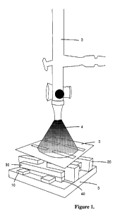
Fig. 1 is a diagram that depicts the modified PEDOT:PSS as it is sprayed onto
the substrate
through a stainless steel shadow mask with an airbrush. Nitrogen is used as
the carrier gas at
a pressure of 20 psi.
Fig. 2 is a diagram showing a perspective view of the novel inverted OPV cells
containing
sprayed-on layers.
Fig. 3 is a graph comparing the voltage versus current plots of the novel
inverted OPV and a
control device fabricated by means of conventional bottom-up structure.
Fig. 4 is a diagram showing the novel organic photovoltaic cell as it receives
photons having
energy hv.
6
CA 02812559 2013-03-25
WO 2012/044971
PCT/US2011/054290
Figure 5 is a graph showing voltage versus current and shows how the Cs3003
layer affects
the performance of the inverted cells when there is no Cs3CO3 layer and with
the Cs3CO3
layer but at different spin rates.
Figure 6 is a graph showing the transmission spectra of PEDOT:PSS with 5% DMSO
at
different spray thickness indicated, the range of thickness from 500nm to
1urn, and
transmittance at 550nm 60-60%.
Figure 7 is a graph showing a comparison of the transmittance between ITO and
the spray-on
anode of m-PEDOT (modified PEDOT:PSS) with different thicknesses.
Figure 8 is a graph showing a comparison of the sheet resistance between ITO
and the
spray-on anode of m-PEDOT (modified PEDOT:PSS) with different thicknesses.
Fig. 9 is a graph showing the transmission spectra of an active layer
(P3HT:PCBM) of 200 nm
(black line with filled square), and with a m-PEDOT:PSS layer of 600 nm (grey
line with filled
circle).
Figure 10 is a graph showing the voltage versus current, indicating how
different m-PEDOT
layer compositions affect the performance of the inverted photovoltaic cell.
Fig. 11 is a graph showing the /-V characteristics of three test cells
measured with AM1.5
solar illumination under different annealing conditions; 1-step annealing at
either 120 C (light
grey circle), or 160 C (black filled square) for 10min; 2-step annealing at
120 C for 10 min,
followed by high vacuum for 1 h and annealing at 160 C for 10 min (medium
grey triangle).
Fig. 12 is a graph showing the I PCE of the three test cells of Figure 5a
under tungsten lamp
illumination. Different annealing conditions were 1-step annealing at either
120 C (light grey
circle), or 160 C (black filled square) for 10min; 2-step annealing at 120 C
for 10 min,
followed by high vacuum for 1 h and annealing at 160 C for 10 min (medium
grey triangle).
Figure 13 is a diagram showing the cross sectional view of the device
architecture of an
inverted solar array showing series connection
Figure 14 is a graph showing the /-V characteristics of 4 inverted spray-on
solar arrays
measured with AM1.5 solar illumination under various annealing conditions: 1-
step annealing
at 120 C (dashed line), or 160 C (thin grey line), and 2-stepannealing
(black filled square).
These 3 arrays use m-PEDOT 750 as the anode. The 4th array (thick black line)
used m-
PEDOT 500 as the anode and was annealed at 160 C.
7
CA 02812559 2013-03-25
WO 2012/044971
PCT/US2011/054290
Fig. 15 is a graph showing the /¨V characteristics of an inverted solar array
under continuous
AM1.5 solar illumination. The first measurement (dashed black line) was done
right after the
array was fabricated and encapsulated. The inset shows the time dependence of
I¨V
characteristics of a spray-on test cell (without encapsulation).
DETAILED DESCRIPTION OF THE PREFERRED EMBODIMENT
There are two different approaches in inverted geometry. One approach is
completely ITO-
free, using a wrap-through method by Zimmermann et.al. (Zimmermann, et al.,
ITO-free wrap
through organic solar cells¨a module concept for cost-efficient reel-to-reel
production, Sol.
Energy Mater. Sol. Cells 91 (2007) 374-378), or the use of a Kapton foil and
an
Aluminum/Chromium bi-layer system as electron contact (Manceau, et al., ITO-
free flexible
polymer solar cells: from small model devices to roll-to-roll processed large
modules, Org.
Electron. 12 (2011) 566-574), and the formation of a bottom electrode
comprising silver
nanoparticles on a 130 um thick polyethyleneternaphthalate (PEN) substrate by
Krebs et.al.
(Krebs, All solution roll-to-roll processed polymer solar cells free from
indium-tin-oxide and
vacuum coating steps, Org. Electron. 10 (2009) 761-768). Another approach is
to add an
electron transport layer onto ITO to make it function as a cathode. Inverted
geometry OPVs in
which the device was first built from modified ITO as cathode have been
studied both in single
cells (Huang, et al., A Semi-transparent plastic solar cell fabricated by a
lamination process,
Adv. Mater. 20 (2008) 415-419; Yu, et al., Efficient inverted solar cells
using TiO2 nanotube
arrays, Nanotechnology 19 (2008) 255202-255207; Li, et al., Efficient inverted
polymer solar
cells, Appl. Phys. Lett. 88 (2006) 253503-253506; Zou, et al., Metal
grid/conducting polymer
hybrid transparent electrode for inverted polymer solar cells, Appl. Phys.
Lett. 96 (2010)
203301-203304; Waldauf, et al., High efficient inverted organic photovoltaics
using solution
based titanium oxide as electron selective contact, Appl. Phys. Lett. 89
(2006) 233517-
233520; Zhou, et al., Inverted and transparent polymer solar cells prepared
with vacuum-free
processing, Sol. Eng. Sol. Cells 93 (2009) 497-500) and solar modules (Krebs
and Norrman,
Using light-induced thermocleavage in a roll-to-roll process for polymer solar
cells, ACS Appl.
Mater. Interfaces 2 (2010) 877-887; Krebs, et al., A roll-to-roll process to
flexible polymer
solar cells: model studies, manufacture and operational stability studies, J.
Mater. Chem. 19
(2009) 5442-5451; Krebs, et al., Large area plastic solar cell modules, Mater.
Sci. Eng. B 138
(2007) 106-111).
OPV single cell utilizing spray technique has been previously reported
(Weickert, et al.,
Spray-deposited PEDOT:PSS for inverted organic solar cells, Sol. Energy Mater.
Sol. Cells
94 (2010) 2371-2374; Kim, et al., Performance optimization of polymer solar
cells using
electrostatically sprayed photoactive layers, Adv. Funct. Mater. 20 (2010)
3538-3546; Kim, et
8
CA 02812559 2013-03-25
WO 2012/044971
PCT/US2011/054290
al., Substrate heated spray-deposition method for high efficient organic solar
cell: morphology
inspection, Jap. J. Appl. Phys. 49 (2010) 01800-01804). However, all these
works involve
either the use of high vacuum deposition, and/or spin-coating process. The
present invention
is the first inverted solar array fabricated by spray. Comparing with
conventional technology
based on spin-coating and using metal as a cathode contact, which greatly
limits
transparency of solar cells and posts difficulty for large scale
manufacturing, the new spray
technology solves these two problems simultaneously. A thin film organic solar
array is
fabricated employing this layer-by-layer spray technique onto desired
substrates (can be rigid
as well as flexible). This technology eliminates the need for high vacuum,
high temperature,
low production rate and high-cost manufacturing associated with current
silicon and in-organic
thin film photovoltaic products. Furthermore, this technology could be used on
any type of
substrate including cloth and plastic.
As used herein, "about" means approximately or nearly and in the context of a
numerical
value or range set forth means 15% of the numerical.
As used herein, "substantially" means largely if not wholly that which is
specified but so close
that the difference is insignificant.
All masks described herein for spray were custom made by Towne Technologies,
Inc.
The incident photon converted electron (IPCE), or the external quantum
efficiency (EQE), of
the device was measured using 250W tungsten halogen lamp coupled with a
monochromator
(Newport Oriel Cornerstone 1/4m).
The photocurrent was detected by a UV enhanced silicon detector connected with
a Keithley
2000 multimeter. The transmission spectrum of active layer was performed on
the same
optical setup.
Example 1
An indium tin oxide (ITO) with and Corning low alkaline earth boro-
aluminosilicate glass
substrate (Delta Technology, Inc.) having a nominal sheet resistance of 4-10
D/square was
pre-cut 4" x 4" , and patterned using a positive photo resist, Shipley 1813,
spin coated at 4500
rpm and soft baked on a hotplate for 3 minutes at 90 C. The structure was then
exposed to a
UV lamp for 1.4 seconds using a constant intensity mode set to 25 watts. The
structure was
developed for about 2.5 minutes using Shipley MF319, rinsed with water, and
hard-baked at
145 C for 4 minutes. Any excess photoresist was cleaned off with acetone and
cotton. The
substrate was etched 5-11 minutes with a solution of 20% HCI and 7% HNO3 at
100 C. The
9
CA 02812559 2013-03-25
WO 2012/044971
PCT/US2011/054290
structure was removed from etchant and cleaned by hand using acetone followed
by
isopropanol. The structure was further cleaned using UV-ozone for at least
fifteen minutes.
A Cs2CO3 interfacial buffer layer was prepared by making a solution of 0.2%
wt. (2 mg/mL)
Cs2CO3 (Aldrich) in 2-ethoxyethanol, and stirring the solution for one hour.
Cs2CO3 was
chosen to reduce ITO work function close to 4.0 eV to be utilized as cathode.
The layer was
applied to the substrate by spray coat using N2 set to 20 psi from a distance
of about 7-10
centimeters. The product was then annealed for 10 minutes at 150 C in an N2
glovebox
(MBraun MOD-01).
The active layer solution was prepared by mixing separate solutions of poly(3-
hexylthiophene)
(P3HT; Riekie Metals, Inc., Lincoln, NE; average molecular weight of 42 K and
regioregularity
over 99%) and 6,6-phenyl C61 butyric acid methyl ester (PCBM; C60, Nano-C,
Inc.,
Westwood, MA; 99.5% purity) in dichlorobenzene at 20 mg/mL. The two solutions
were
stirred on a hotplate for 24 hours at 60 C, and then the solutions were mixed
together at a 1:1
ratio. The mixture was stirred for an additional 24 hours at 60 C, producing a
final solution of
10 mg/mL.
The active coating is prepared by spray coating using N2 set to thirty 30 psi
from a distance of
about 7-10 centimeters. Multiple light layers were sprayed onto the structure
first, at about
600-900 pm per spray. A final thick continuous coat was then applied to
complete the active
layer coating having a final layer thickness of about 200-300 nm. A cotton
cloth with DCB
was used to wipe excess from the substrate. The structure was then wiped with
a cotton
cloth in isopropanol. The substrate was then dried in an antechamber under
vacuum for at
least twelve 12 hours.
A kovar shadow mask was aligned into position and taped onto the substrate.
The series
connection locations were then wiped using a wooden dowel.
The anodic buffer layer was prepared using a modified poly (3,4)
ethylenedioxythiophene
(PEDOT) and poly(styrenesulfonate) (PSS) solution (PEDOT:PSS; Baytron 500 and
750;
H.C. Starck GmbH., Munich, Germany). The PEDOT:PSS was diluted and filtered
out through
a 0.45 um filter. This filtered solution of PEDOT:PSS was mixed with 5 vol% of
dimethylsulfoxide and was stirred at room temperature followed by one 1 hour
of sonification
to form a modified PEDOT:PSS (mPED). The solution PEDOT:PSS, when used alone,
has a
relatively low conductivity that reduces device performance. The conductivity
of PEDOT:PSS
was increased by doping it with dimethylsulfoxide.
Mask 2 was placed onto the cell containing anode 10, interfacial layer 40 and
active layer 30.
The mPED coating was prepared by placing the substrate/mask on a hotplate at
90 C. The
substrate/mask was spray coated with spray device 3, using nitrogen (N2) as
the carrier gas,
CA 02812559 2013-03-25
WO 2012/044971
PCT/US2011/054290
set to 30 psi from a distance of about seven to ten centimeters 7-10 cm, as
seen in Figure 1.
Multiple light layers of spray 4 were applied until the final thickness is
reached. The substrate
was then removed from the hotplate and the mask is removed. Care was taken to
avoid
removing the mPED with the mask.
The substrate is then subjected to a high vacuum (10-6 Torr) for 1 hour, which
improved the
device performance with the sprayed active layer (Lim, et al., Spray-deposited
poly(3,4-
ethylenedioxythiophene):poly(styrenesulfonate) top electrode for organic solar
cells, Appl.
Phys. Lett. 93 (2008) 193301-193304). After the vacuum, the device was
annealed for 10
minutes at 120 C. The vacuuming and annealing steps were then repeated a
second time, at
the same conditions. The substrate was finally encapsulated by applying silver
paint to the
device contacts or a UV-cured encapsulant (EPO-TEK 0G142-12; Epoxy Technology,
Inc.,
Biiierica, MA) and allowing the paint to dry. The encapsulated glass was then
notched and
cleaned by hand using acetone and isopropanol, followed by at least 15 minutes
of UV-ozone
cleaning. The encapsulated glass was then placed into the glovebox, together
with a small
quantity of UV-cure epoxy and a paintbrush. The UV-cure epoxy is applied with
the
paintbrush to the edge of the encapsulation glass. The device was then
inverted and placed
on top of the encapsulation glass. The device is then exposed to UV-ozone for
15 minutes to
cure the encapsulate epoxy.
Inverted organic photovoltaic cell 1, seen dissected in Figure 2, was created
using the method
described above. Inverted photovoltaic cell 1 was composed of different layers
of active
materials and terminals (anode and cathode) built onto substrate 5. Anode 10,
comprised of
ITO in the present example, was sprayed onto substrate 5 forming a `I I'
pattern extending
from a first set of edges of substrate 5. Interfacial buffer layer 40 covers
anode 10, except for
the outermost edges, as seen in Figure 2. The components of the interfacial
buffer layer were
chosen to provide a gradient for charges crossing the interface, approximating
a conventional
p-n junction with organic semiconductors, thereby providing an increased
efficiency of
heterojunctions. An exemplary interfacial layer is composed of Cs2CO3, ZnO, or
titanium
oxide. Active layer 30 is disposed directly on top of interfacial buffer layer
40, and was
prepared using poly(3-hexylthiophene) and 6,6-phenyl C61 butyric acid methyl
ester. Anode
20 was disposed on the active layer in a pattern, similar to the cathode, but
perpendicular to
the cathode. Exemplary anode materials include PEDOT:PSS doped with
dimethylsulfoxide.
The fully encapsulated 4 um X 4 um array was found to possess over 30%
transparency.
The device was analyzed against a control device fabricated by means of
conventional
bottom-up structure using a metal cathode by thermo evaporation. At this
stage, the novel
11
CA 02812559 2013-03-25
WO 2012/044971
PCT/US2011/054290
inverted cell has smaller PCE (1.3%) than that of the control device (3.5%),
as seen in Figure
3.
Example 2
The photovoltaic cell was tested to determine its photoelectric generation.
The organic
photovoltaic cell was exposed to photons having energy hv, as seen in Figure
4. No spectral
mismatch with the standard solar spectrum was corrected in the power
conversion efficiency
(PCE) calculation.
The current-voltage (I-V) characterization of the solar array was performed
using a Newport
1.6 KW solar simulator under AM1.5 irradiance of 100 mW/cm2. In order to have
a good
reference point for the multi-cell array, the inverted single-cell test
device, consisted of four
identical small cells (4 mm2) on a 1" X 1" substrate, using m-PEDOT 500 as
anode. Figure 5
shows how the Cs2CO3 layer affects the performance of the inverted cell. The
control cell
without Cs2CO3 (black circle) performed almost like a resistor and had
negligible Voc (0.03 V).
The lower performance was due to non-ohmic contact with the cathode, with
reduced built-in
electric field across the active layer. For a better controlled thickness,
Cs2CO3 was spin-
coated onto the cleaned ITO substrate in these devices. As shown in Figure 5,
the optimal
thickness of Cs2CO3 layer was achieved at a spin rate of 5000 rpm. At higher
rate of 7000
rpm, the device was less efficient owing to the fact of a discontinuous Cs2CO3
layer. It was
further noted that the optimal thickness is between 10 and 15 A measured by
AFM
topography.
ITO normally has a work function of -4.9 eV, and is traditionally used as an
anode in typical
OPV devices. There have been previous reports on tuning the work function of
ITO by adding
an electron transport layer such as ZnO (Zou, et al., Metal grid/conducting
polymer hybrid
transparent electrode for inverted polymer solar cells, Appl. Phys. Lett. 96
(2010) 203301-
203304), TiO2 (Huang, et al., A Semi-transparent plastic solar cell fabricated
by a lamination
process, Adv. Mater. 20 (2008) 415-419; Yu, et al., Efficient inverted solar
cells using TiO2
nanotube arrays, Nanotechnology 19 (2008) 255202-255207; Li, et al., Efficient
inverted
polymer solar cells, Appl. Phys. Lett. 88 (2006) 253503-253506), PEO (Zhou, et
al., Inverted
and transparent polymer solar cells prepared with vacuum-free processing, Sol.
Eng. Sol.
Cells 93 (2009) 497-500) and Cs2CO3 (Huang, et al., A Semi-transparent plastic
solar cell
fabricated by a lamination process, Adv. Mater. 20 (2008) 415-419; Yu, et al.,
Efficient
inverted solar cells using TiO2 nanotube arrays, Nanotechnology 19 (2008)
255202-255207;
Li, et al., Efficient inverted polymer solar cells, Appl. Phys. Lett. 88
(2006) 253503-253506) in
inverted OPV single cells. Previous report showed Cs2CO3 can lower the ITO
work function to
as low as 3.3 eV. By spin coating a solution of 2-ethoxyethanol with 0.2%
Cs2CO3 at 5000
12
CA 02812559 2013-03-25
WO 2012/044971
PCT/US2011/054290
rpm for 60 s, a very thin layer (-10A) of Cs2003 is formed over the ITO. It
was reported that a
dipole layer would be created between Cs2CO3 and ITO. The dipole moment helped
to reduce
the work function of ITO, allowing ITO to serve as the cathode.
To estimate of the effective work function of ITO/Cs2CO3 cathode, a control
device was
fabricated with 100 nm aluminum cathode deposited on glass substrate, with the
active layer
and m-PEDOT layer fabricated the same way as in ITO/Cs2CO3 cathode
configuration
described above. Since aluminum is not transparent, the I-V in both devices
were measured
by illumination from m-PEDOT side using the same illumination condition for
the Aluminum
control and the ITO/Cs2CO3 cathode device. The Voc of the Aluminum cathode
control device
was 0.24 V, whereas the Voc of the ITO/ Cs2CO3 cathode device spun at 7000 rpm
was 0.36
V, as seen in Figure 5. Since aluminum has work function of 4.2 eV, this
indicates that, the
effective work function of ITO/Cs2CO3 is close to 4.1 eV.
Example 3
Different compositions of PEDOT:PSS were analyzed to determine optimum active
layer
constituents. Photovoltaic cells were prepared similarly to the methods
described in Example
1, with PH-500 modified 5% DMSO. The transmission spectra of the sprayed-on
mPEDOT
was measured for different wavelengths, using different thicknesses of active
layer, as seen
in Figure 6. Figures 7 and 8 show how the thickness of the sprayed-on m-PEDOT
layer
affects its transmittance and sheet resistance. Transmittance was measured
using a 250W
tungsten halogen lamp coupled with a monochromator (Newport Oriel Cornerstone
1/4 m).
ITO was chosen as a reference for comparison. At a thickness of about 100 nm,
the
transmittance of m-PEDOT is about 80%, comparable with ITO, as seen in Figure
7. The
sheet resistance of m-PEDOT was measured using a standard four-point probe
measurement
(Van Zant, Microchip Fabrication, McGraw-Hill, New York, ISBN 0-07-135636-3,
2000, pp.
431-2; van der Pauw, A method of measuring the resistivity and Hall
coefficient on lamellae
of arbitrary shape, Philips Tech. Rev. 20 (1958) 220-224). As expected, the
resistance
decreases as thickness increases, which is consistent with the bulk model, as
seen in Figure
8.
These two parameters (transmittance and sheet resistance) are important to
assess the
feasibility of m-PEDOT to be used as a replacement contact for the
conventional metal
contact. The trade-off between transparency and resistance is another
important fabrication
parameter. The current array was fabricated with thickness of about 600 nm,
which has
moderate resistance of 70 0/square, and transmittance about 50%.
13
CA 02812559 2013-03-25
WO 2012/044971
PCT/US2011/054290
The transmission spectra of the active layer (P3HT:PCBM, 200 nm) and m-PEDOT
anode of
600 nm were compared, as seen in Figure 9. The total transmittance over the
spectra range
shown decreases from 73% to 31% after spraying on the m-PEDOT anode.
Photovoltaic cells were manufactured using different PEDOT compositions (PH-
500 and PH-
750) modified with 5% DMSO. The remaining procedures were followed as provided
in
Example 1, and the performance measured as disclosed above. As seen in Figure
10,
performance for PH-750 showed a strong initial current, which decreased with
increasing
voltage. Conversely, PH-500 performed poorly at lower voltages, but better
than PH-750 at
higher voltage.
Example 4
Annealing has shown to be the most important factor to improve organic solar
cell
performance. Photovoltaic cells were prepared as described above, except with
the annealing
occurring in one step at 120 C for 10 min., one step at 160 C for 10 min, or
a two-step
annealing at 120 C for 10 min followed by high vacuum for 1 hour and then 160
C for 10
min. Figures 11 and 12 show the comparison of current¨voltage (I¨V) and
incident photon
converted electron (IPCE) or external quantum efficiency (EQE) between three
inverted test
cells at the different annealing conditions. The rationale behind choosing
such annealing
conditions was to experiment both annealing temperature and the thermal
profile. Figure 11
shows that 1-step annealing at 120 C gives the best result in test cell, with
Voc = 0.48 V, lõ =
0.23 mA, FF = 0.44, and a power conversion efficiency (PCE) of 1.2% under
AM1.5 solar
illumination with intensity 100 mW/cm2. The second annealing step at 160 C
worsens the
device performance, mainly due to unfavorable change of film morphology, which
was
confirmed in AFM images, data not shown. The PCE of 1-step annealing at 160 C
was in
between 1-step annealing at 120 C and 2-step annealing, yet the device has
the worst FF.
Table 1 listed the details of the I¨V characteristics of these three test
cells.
Table 1. Test cell /-Vcharacteristics comparison at various annealing
conditions.
Test cell /õ(mA) Võ (V) FF r (%) Annealing condition
number
1 0.28 0.48 0.26 0.86 160 C, 10 min
2 0.23 0.48 0.44 1.2 120 C, 10 min
3 0.16 0.30 0.35 0.43 2-step
14
CA 02812559 2013-03-25
WO 2012/044971
PCT/US2011/054290
In Figure 12, IPCE measurement shows 2-step annealing was worse than 1-step
annealing,
which was consistent with the I¨V measurements, not shown. There seems to be
some
inconsistency between PCE and IPCE for the cells annealed at 160 and 120 C,
as the cells
annealed at 160 C have higher IPCE yet lower PCE than that at 120 C. IPCE
measurement
was done under illumination from the Tungsten lamp, whereas I¨V was done under
solar
simulator, which has a different spectrum than that of the tungsten lamp.
Nevertheless, the
integration of IPCE should be proportional to Isc. The device made by 1-step
annealing at 160
C, though having smaller power conversion efficiency, actually has larger Isc
(0.28mA) than
the one at 120 C (0.23 mA). The ratio between integral of IPCE at 160 C vs.
120 C is about
1.3, and the ratio of Isc of the same devices was 1.2. Without being limited
to any theory, the
slight discrepancy might also come from the fact that the cells behave
differently under strong
(IV) and weak (IPCE) illuminations. Usually bi-molecular (BM) recombination
sets in under
high light intensity (solar simulator) (Shaheen, et al., 2.5% efficient
organic plastic solar cells,
Appl. Phys. Lett. 78 (2001) 841-843), meaning the cell, which has more
prominent BM
recombination, will perform poorer with high intensity illumination such as
that from the solar
simulator. It might be that the cell annealed at 160 C was affected by BM
recombination
more than the cell annealed at 120 C, due to more traps associated with
rougher
morphology, data not shown, serving as recombination centers. The same
mechanism can
also be applied to explain the larger difference in IPCE of device annealed at
160 C and by
2-step annealing than that of their Isc in Figures 11 and 12.
1-step annealing at 120 C (b) showed improved film roughness and the best
phase
segregation of P3HT and PCBM, which explains the high device performance using
this
annealing profile, as seen in Figures 11 and 12. Device by 2-step annealing
has the
smoothest film, however, the phase segregation was much less distinct. This
indicates that
P3HT chains and PCBM molecules are penetrating through each other more after
the second
annealing at 160 C, and form much smaller nano-domains, which are favorable
for charge
transport between the domains (Kline and McGehee, Morphology and charge
transport in
conjugated polymers, J Macromol. Sci. C: Polym. Rev. 46 (2006) 27-45).
However,
recombination of photogenerated carriers might be enhanced due to the lack of
separate
pathways for electron sand holes, and that was why the device after 2-step
annealing
performed worse than after the 15' annealing at 120 C, seen in Figures 11 and
12. 1-step
annealing at higher temperature of 160 C results in the roughest film (even
rougher than the
as-made device), and the P3HT phase and PCBM phase are hardly distinguishable.
This
rough film also further affects the interface between active layer and m-
PEDOT, resulting in
poor FF of the device, seen in Figures 11 and 12.
Example 5
CA 02812559 2013-03-25
WO 2012/044971
PCT/US2011/054290
Solar illumination has been demonstrated to improve solar array efficiency up
to 250%.
Device efficiency of 1.80% was observed with the array under AM1.5 irradiance.
Our
preliminary data have shown that the performance enhancement under
illumination only
happens with sprayed devices, not devices made by spin coating. This means
that solar cells
made with our spray-on technique performs better under sunlight, which is
beneficial for solar
energy application.
A solar array was prepared by forming 50 individual inverted cells, each with
an active area of
60 mm2, and using either m-PEDOT 750 or m-PEDOT 500 as the semitransparent
anode.
The array was configured with 10 cells in series in one row to increase the
voltage, and five
rows in parallel connection to increase the current. The neighboring cells
were connected
using the organic layer configuration, seen in cross section in Figure 13.
Characteristics of the arrays were tested as described above. The I-V of four
arrays
prepared using the different annealing conditions described in Example 4,
above, were
measured with AM1.5 solar illumination, seen in Figure 14. It is clear that 1-
step annealing at
low temperature (120 C) gives the worst result, and 2-step annealing showed
improved I-V
characteristics (Voc, Jsc, FF and PCE) after the second high temperature
annealing at 160 C.
1-step annealing at high temperature (160 C) gives the best Voc, and 2-step
annealing yields
the highest J5c. In terms of anode, m-PEDOT 500 seems to give higher Voc than
PEDOT 750,
as seen in Table 2. However, there is not much difference of PCE between 2-
step annealing
and 1-step annealing at 160 C, which is in contrast with the result of the
test device, seen in
Figures 11 and 12. We think the annealing duration is probably too short for
the array, since it
has much larger area and contains much more materials. Further investigation
of interplay
between annealing temperature, duration and thermal profile is ongoing to find
the optimal
device fabrication conditions.
Table 2. Array I-V characteristics comparison at various annealing conditions.
Array isc (mA) Voc (V) FF r (0/0) Annealing m-
PEDOT
number condition
1 17.0 3.9 0.30 0.68 2-step 750
2 11.5 4.0 0.39 0.62 2-step 750
3 6.30 2.8 0.37 0.22 2-step 750
4 13.0 4.0 0.33 0.56 160 C 10 min
750
5 15.0 5.2 0.33 0.86 160 C 10 min
500
6 12.0 5.8 0.30 0.70 160 C 10 min
500
7 11.1 5.2 0.35 0.67 160 C 10 min
500
Number of coats for spray-on active layer: 5 light layers, and 2 heavy layers
Number of coats for the spray-on PEDOT:PSS layer:6-7 light layers, and 5 heavy
layers
Number of coats for the spray-on Cs2CO3 layer: 1 light layer
16
CA 02812559 2013-03-25
WO 2012/044971
PCT/US2011/054290
An interesting phenomenon was observed with the inverted organic photovoltaic
cells, which
is termed 'photo annealing', seen in Figure 15. Under constant illumination
from the solar
simulator, a sudden change in I¨V characteristics occurs after time, which is
device
dependent, ranging from 10 min to several hours. For example, the solar array
shown in
Figure 15 required about 15 min to 'photo anneal', and reached a maximum PCE
after 2.5 h
Table 3. change of array 1-V characteristics under solar illumination.
Time isc (mA) V0( V) FF
Day 1
-0 min 17 4.0 0.30 0.68
-12 min 28 4.2 0.35 1.40
-150 min 35 4.2 0.37 1.80
Day 2
-0 min 18 4.2 0.35 0.88
Day 3
-0 min 15 4.4 0.29 0.64
-120 min 27 4.8 0.38 1.68
It was also noted that this sudden increase of Isc was accompanied by a
characteristic
17
CA 02812559 2013-03-25
WO 2012/044971
PCT/US2011/054290
conjugated polymers of high intrachain order, Phys. Rev. B 54 (1996) 7610-
7613; Nelson,
Organic photovoltaic films, Curr. Opinion Solid State Mater. Sci. 6 (2002) 87-
95). The
wiggling of the I-V data indicate the non-uniformity of the film morphology,
and the overall
boost of device performance is the result of the free-up of previously trapped
charges in the
active layers. This observation is against the conventional picture of organic
solar cell, which
normally shows degradation under solar illumination (Dennler, et al., A new
encapsulation
solution for flexible organic solar cells, Thin Solid Films 511-512 (2006) 349-
353).
Surprisingly, this performance enhancement under illumination only happened
with sprayed
devices, not with a device made by spin coating. As such, solar cells prepared
using the
spray-on technique performs better under sunlight, which is obviously
beneficial for solar
energy application. The thermal annealing was important in improving device
PCE.
Moreover, the optimal annealing conditions are not the same with small single
cell and large
solar array consisting of 50 cells. Systematic study of optical, electronic
and morphologic
properties of the device revealed the influence of nanomorphology over device
power
conversion efficiency. Moreover, the photo annealing, i.e., more than 2-fold
increase of solar
cell PCE under solar irradiance and with hysteresis pattern, is in contrary to
the normal
understanding of organic solar cell degradation under sunlight. The fact that
photo annealing
was only observed with sprayed solar cell or arrays places an advantageous
solution to for
large scale, low-cost solution-based solar energy applications.
In the preceding specification, all documents, acts, or information disclosed
do not constitute
an admission that the document, act, or information of any combination thereof
was publicly
available, known to the public, part of the general knowledge in the art, or
was known to be
relevant to solve any problem at the time of priority.
The disclosures of all publications cited above are expressly incorporated
herein by
reference, each in its entirety, to the same extent as if each were
incorporated by reference
individually.
While there has been described and illustrated specific embodiments of an
organic
photovoltaic cell and methods of manufacturing the photovoltaic cell, it will
be apparent to
those skilled in the art that variations and modifications are possible
without deviating from
the broad spirit and principle of the present invention. It is also to be
understood that the
following claims are intended to cover all of the generic and specific
features of the invention
herein described, and all statements of the scope of the invention which, as a
matter of
language, might be said to fall therebetween.
18