Note: Descriptions are shown in the official language in which they were submitted.
CA 02812742 2015-08-06
54590-18
1
DESCRIPTION
Title of Invention
OPTICAL COMPONENT AND METHOD OF MANUFACTURING THE SAME
Technical Field
[0001]
The present invention relates to an optical component and a method of
manufacturing the optical component.
Background Art
[0002]
In recent years, for spectacle lenses, plastic lenses have been used in many
cases due to advantages such as lightweight, excellent impact resistance, and
ease of dyeing.
In the plastic lens for use in a spectacle lens, an antireflection film is
generally provided on
both sides of the plastic lens for the purpose of preventing surface
reflection. Generally, the
antireflection film for a spectacle lens has a low reflection characteristic
(wideband low-
reflection characteristic) over the entire visible region of 400 nm to 700 nm.
[0003]
In the case of an optical component such as a spectacle lens, an optical
component which is provided with a plastic base and an antireflection film
disposed on the
base as disclosed in, for example, Patent Documents 1 to 3 is known.
= CA 02812742 2013-03-26
2
Citation List
Patent Document
[0004]
[Patent Document 1] Japanese Unexamined Patent Application, First
Publication No. H11-30703
[Patent Document 2] Japanese Unexamined Patent Application, First
Publication No. 2006-251760
[Patent Document 3] Japanese Unexamined Patent Application, First
Publication No. 2007-127681
Summary of Invention
Technical Problem
[0005]
However, from recent studies, it is known that the low reflection
characteristic
over the entire visible region is not necessarily desirable for visibility and
eye health.
Glare is reduced, and visibility and contrast are improved by cutting the blue
region (380
nm to 500 nm) of visible light.
In addition, regarding eye health, since the blue region (380 nm to 500 nm) of
visible light has a high intensity of energy, it is said to be a cause of
impact to the retina
and the like. The impact caused by blue light is referred to as "blue light
hazard".
Particularly, the most undesired region is about 435 nm to about 440 nm, and
it is said
that it is desirable to cut the light in this region.
[0006]
Recently, in liquid crystal screens that have become the mainstream of
displays
and LED illumination, a lot of light with a wavelength of about 450 nm is
emitted, and
. CA 02812742 2013-03-26
3
thus control of such light rays in the blue region has attracted attention. As
means for
cutting the blue region (380 nm to 500 nm) of visible light, a dyed lens such
as
sunglasses is known. However, in the dyed lens, the entire visible region is
cut, and
thus visibility deteriorates due to a reduction in light intensity.
[0007]
An object of an aspect of the invention is to provide an optical component
which
has an antiglare effect, is effective for a reduction in feeling of fatigue
and prevention of
eye trouble, and is excellent in visibility, and a method of manufacturing the
optical
component.
Solution to Problem
[0008]
.
An optical component according to an aspect of the invention includes: a
plastic
base which has a convex surface and a concave surface; and a multilayer film
which is
_
disposed on at least the convex surface of the plastic base, the multilayer
film having an
average reflectivity of 2% to 10% over a wavelength range of 400 nm to 500 nm.
[0009]
In addition, a method of manufacturing an optical component according to an
aspect of the invention is a method of manufacturing the optical component
which
includes a plastic base which has a convex surface and a concave surface and a
multilayer film which is disposed on at least the convex surface of the
plastic base. The
method includes the steps of: heating the plastic base; and forming the
multilayer film on
the plastic base after adjusting the temperature of the plastic base to a
predetermined
temperature by the heating step. The step of forming the multilayer film has a
process
of forming a high refractive index layer having a multilayer structure by
alternately
applying a high refractive index material and a low refractive index material
in
CA 02812742 2015-08-06
54590-18
4
multilayers, and a process of forming, on the high refractive index layer, a
low refractive
index layer having a lower refractive index than that of the high refractive
index layer, and
wherein an average reflectivity of the multilayer film over a wavelength range
of 400 nm to
500 nm is 2% to 10%.
[0009a]
According to an aspect of the invention, there is provided a spectacle lens
comprising: a plastic base which has a convex surface and a concave surface;
and a
multilayer film which is disposed on at least the convex surface of the
plastic base, wherein
the multilayer film has an average reflectivity of 4.2% to 10% over a
wavelength range of
400 nm to 500 nm.
[0009b]
According to another aspect of the invention, there is provided a method of
manufacturing the spectacle lens according to the above aspect of the
invention which
includes a plastic base which has a convex surface and a concave surface and a
multilayer
film which is disposed on at least the convex surface of the plastic base, the
method
comprising the steps of: heating the plastic base; and forming the multilayer
film on the
plastic base after adjusting the temperature of the plastic base to a
predetermined temperature
by the heating step, wherein the step of forming the multilayer film has a
process of forming a
high refractive index layer having a multilayer structure by alternately
applying a high
refractive index material and a low refractive index material in multilayers,
and a process of
forming, on the high refractive index layer, a low refractive index layer
having a lower
refractive index than that of the high refractive index layer, and wherein an
average
reflectivity of the multilayer film over a wavelength range of 400 nm to 500
nm is 4.2% to
10%.
CA 02812742 2015-08-06
54590-18
4a
[0010]
According to an optical component of an aspect of the invention, a sufficient
antiglare effect is obtained while maintaining excellent visibility.
In addition, according to a method of manufacturing an optical component of
an aspect of the invention, an optical component with reduced glare, with
which it is easy to
see, and which has optical characteristics effective for prevention of fatigue
and eye trouble
can be provided.
Brief Description of Drawings
[0011]
1 0 FIG. 1 is a schematic diagram showing an example of an optical
component
according to a first embodiment.
FIG. 2 is a schematic diagram showing an example of an optical component
according to a second embodiment.
FIG. 3 is a schematic diagram showing an example of a deposition device
1 5 according to the first embodiment.
FIG. 4 is a graph showing a spectral characteristic of an antireflection film
according to Example 1.
FIG. 5 is a graph showing a spectral characteristic of an antireflection film
according to Example 2.
= CA 02812742 2013-03-26
FIG. 6 is a graph showing a spectral characteristic of an antireflection film
according to Example 3.
FIG. 7 is a graph showing a spectral characteristic of an antireflection film
according to Comparative Example 1.
5 FIG. 8 is a graph showing a spectral characteristic of an
antireflection film
according to Example 4.
FIG. 9 shows results of a comparative wearing evaluation according to Test 2.
FIG. 10 is a graph showing a spectral characteristic of an antireflection film
according to Example 5.
FIG. 11 is a graph showing a spectral characteristic of a convex surface of an
antireflection film according to Example 6.
FIG. 12 is a graph showing a spectral characteristic of a concave surface of
the
antireflection film according to Example 6.
FIG. 13 is a graph showing a spectral characteristic of a convex surface of an
antireflection film according to Example 7.
FIG. 14 is a graph showing a spectral characteristic of a concave surface of
the
antireflection film according to Example 7.
FIG. 15 shows results of a comparative wearing evaluation according to Test 3.
Description of Embodiments
[0012]
Hereinafter, embodiments of the invention will be described in detail.
The embodiments are described in detail to achieve a better understanding of
the
points of the invention, but the invention is not limited thereto unless
otherwise stated.
[0013]
CA 02812742 2013-03-26
6
(1) First Embodiment
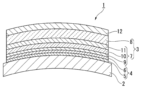
FIG. 1 is a sectional side view schematically showing an optical component of
a
first embodiment of the invention. The reference numeral 1 represents an
optical
component for a spectacle lens.
The optical component 1 is provided with a plastic base 2 and an inorganic
multilayer film 3 disposed on a convex surface of the plastic base 2. In this
embodiment, a functional thin film 4 is disposed between the convex surface of
the
plastic base 2 and the inorganic multilayer film 3. In this embodiment, the
functional
thin film 4 is formed of a primer layer 5 and a hard coating layer 6.
[0014]
In the following description, the films 3 and 4, which are disposed on the
surface
(convex surface) of the plastic base 2, will mainly be described. However,
actually,
films which are the same as the films 3 and 4 formed on the surface (convex
surface) are
also formed on the rear surface (concave surface) of the plastic base 2.
[0015]
The plastic base 2 is made of, for example, transparent plastic such as an
acryl-based resin, a thiourethane-based resin, a methacryl-based resin, an
allyl-based
resin, an episulfide-based resin, a polycarbonate-based resin, a polyurethane-
based resin,
a polyester-based resin, a polystyrene-based resin, an episulfide resin, a
polyethersulfone
resin, a poly-4-methylpentene-1 resin, a diethylene glycol bis ally] carbonate
resin
(CR-39), a polyvinyl chloride resin, a halogen-containing copolymer, and a
sulfur-containing copolymer. In addition, in this embodiment, for example, one
of 1.50,
1.60, 1.67, and 1.74 is selected and used as a refractive index (nd) of the
plastic base 2.
When the refractive index of the plastic base 2 is set to 1.6 or greater, an
allyl
carbonate-based resin, an acrylate-based resin, a methacrylate-based resin, a
CA 02812742 2013-03-26
7
thiourethane-based resin and the like are preferably used for the plastic base
2. In
addition, the plastic base 2 may not be transparent, or may be colored if it
is translucent.
The transmissivity of the colored plastic base 2 is preferably 5% to 85%.
[0016]
The functional thin film 4 is disposed between the plastic base 2 and the
inorganic multilayer film 3 as described above, and is formed of the primer
layer 5 which
is disposed to be brought into contact with the plastic base 2 and the hard
coating layer 6
which is disposed to be brought into contact with the primer layer 5 and the
inorganic
multilayer film 3.
The primer layer 5 is used to improve the adhesion between the plastic base 2
and the hard coating layer 6 and functions as an adhesion layer. In addition,
the primer
4 layer 5 is also used to absorb the impact on the optical
component 1 and functions as an
impact absorption layer.
[0017]
The primer layer 5 contains a polyurethane-based resin as a main component,
and in this embodiment, the primer layer 5 is a polyurethane-based resin
containing, for
example, particulates of an inorganic material. The primer layer 5 may include
at least
one type of an acryl-based resin, a methacryl-based resin, and an
organosilicon-based
resin. The thickness (actual thickness) of the primer layer 5 is preferably
about 0.5 tm
to about 1.0 p.m.
[0018]
Such a primer layer 5 can be formed with a predetermined thickness on the
plastic base 2 by dipping the plastic base 2 in a liquid for forming the
primer layer 5 and
then lifting and drying the plastic base 2. As the liquid for forming the
primer layer 5,
for example, a liquid in which a resin to be the primer layer 5 and an
inorganic oxide
= CA 02812742 2013-03-26
=
8
particulate sol are dispersed or dissolved in water or an alcohol-based
solvent and mixed
therewith can be used.
[0019]
Since the hard coating layer 6 has a function of protecting the plastic base 2
and
suppressing impact to the plastic base 2, it functions as an abrasion-
resistant film.
The hard coating layer 6 is formed of, for example, an organosiloxane-based
hard coating layer. The organosiloxane-based hard coating layer is a layer in
which
particulates of inorganic oxide are dispersed in an organosiloxane-based
resin. As the
inorganic oxide, for example, rutile-type titanium oxide and oxides of
silicon, tin,
zirconium, and antimony are preferably used. In addition, for example, as
disclosed in
Japanese Examined Patent Application, Second Publication No.H4-55615, a
colloidal
silica-containing organosilicon-based resin may be used as the hard coating
layer 6.
The thickness (actual thickness) of the hard coating layer 6 is preferably
about 2 pim to
about 4 Jim.
[0020]
The hard coating layer 6 can be formed with a predetermined thickness on the
primer layer 5 on the plastic base 2 by dipping the plastic base 2 having the
primer layer
5 formed thereon in a liquid for forming the hard coating layer 6 and then
lifting and
drying the plastic base 2. As the liquid for forming the hard coating layer 6,
for
example, a liquid in which a resin to be the hard coating layer 6 and an
inorganic oxide
particulate sol are dispersed or dissolved in water or an alcohol-based
solvent and mixed
therewith can be used.
[0021]
When the refractive index of the functional thin film 4 including the primer
layer
5 and the hard coating layer 6 and the refractive index of the plastic base 2
are almost the
= CA 02812742 2013-03-26
9
same as each other, it is possible to suppress a reduction in transmissivity
and the
occurrence of interference fringes which are caused by the reflection at an
interface
between the functional thin film 4 and the plastic base 2. Accordingly, it is
desirable to
adjust the refractive index of the functional thin film 4 in accordance with
the refractive
index of the plastic base 2. The refractive index of the functional thin film
4 (primer
layer 5 and hard coating layer 6) can be adjusted by selecting the type
(physical
properties) of resin which is a main component of the functional thin film 4,
or by
selecting the type (physical properties) of particulates added to the resin
which is a main
component.
[0022]
In this embodiment, the functional thin film 4 is formed to include the primer
layer 5 and the hard coating layer 6. However, for example, one or both of the
primer
layer 5 and the hard coating layer 6 may be omitted. In addition, as a
constituent film of
_
the functional thin film 4, for example, a dielectric film and a metallic film
made of
indium tin oxide (ITO) or the like may be disposed in addition to the primer
layer 5 and
the hard coating layer 6.
In addition, in this embodiment, a dielectric film or a metallic film having a
thickness of 20 nm or less may be disposed between a high refractive index
inorganic
material and a low refractive index inorganic material constituting the
inorganic
multilayer film. The thickness of the dielectric film or the metallic film may
be 10 nm
or less.
[0023]
The inorganic multilayer film 3 has a double-layer configuration which has a
high refractive index layer 7 having a multilayer structure in which a high
refractive
index inorganic material and a low refractive index inorganic material are
alternately
CA 02812742 2013-03-26
applied in multilayers and a low refractive index layer 8 made of a low
refractive index
inorganic material having a lower refractive index than that of the high
refractive index
layer 7 on the high refractive index layer 7. The inorganic multilayer film 3
functions
as an antireflection film which prevents the reflection of incident light. In
this
5 embodiment, the inorganic multilayer film 3 is designed to have an
average reflectivity
of 2% to 10% over a wavelength range of 400 nm to 500 nm.
When the average reflectivity is in such a range, a sufficient antiglare
effect is
obtained and excellent visibility can be maintained in use as a spectacle
lens. When the
average reflectivity over the wavelength region is 10% or greater, a person
wearing such
10 glasses can experience glare due to the reflection of incident light,
particularly from the
concave surface of the spectacle lens. Therefore, the average reflectivity is
preferably
3% to 10%.
In addition, in this embodiment, an inorganic multilayer film is used as a
multilayer film. However, an organic multilayer film may be used as long as
the
advantageous effect of the invention is not impaired.
[0024]
Furthermore, the inorganic multilayer film 3 is preferably designed to have a
reflectivity of 1.5% or less over a wavelength region of 580 nm to 780 nm. Due
to such
a design, a spectacle lens which has a more effective antiglare effect and
better visibility
can be obtained.
[0025]
In this embodiment, the high refractive index layer 7 is formed of a first
layer 9
made of a high refractive index inorganic material which is provided close to
the plastic
base 2, a second layer 10 made of a low refractive index inorganic material
which is
provided on the first layer 9, and a third layer 11 made of a high refractive
index
CA 02812742 2013-03-26
11
inorganic material which is provided on the second layer 10.
[0026]
The first layer 9 is provided to be brought into contact with the hard coating
layer 6, and is made of zirconium dioxide (Zr02) having a refractive index of
2Ø Other
than Zr02, for example, titanium dioxide (Ti02) and tantalum dioxide (Ta205)
can be
used as the high refractive index inorganic material constituting the first
layer 9.
Furthermore, the first layer 9 can also be made of oxide of an alloy of plural
types
including zirconium, titanium, and tantalum. In addition to these, for
example,
aluminum oxide (A1203), yttrium dioxide (Y203), hafnium dioxide (Hf02), and
niobium
dioxide (Nb205) can also be used.
[0027]
Here, in this manner, when the first layer 9 is made of a high refractive
index
inorganic material (Zr02), the adhesion between the first layer 9 and the hard
coating
layer 6 can be obtained. That is, this is because the adhesion (adhesion
power) between
the layer (Zr02) made of a high refractive index inorganic material and the
hard coating
layer 6 is greater than the adhesion (adhesion power) between the layer (Si02)
made of a
low refractive index inorganic material and the hard coating layer 6. In
addition, even
when the functional thin film 4 (primer layer 5 and hard coating layer 6) is
omitted, the
adhesion (adhesion power) between the high refractive index layer (Zr02) and
the plastic
base 2 is greater than the adhesion (adhesion power) between the low
refractive index
layer (Si02) and the plastic base 2, and thus using a high refractive index
inorganic
material is better for adhesion.
[0028]
The second layer 10 is provided to be brought into contact with the first
layer 9,
and is made of silicon dioxide (Si02) having a refractive index of 1.47. Other
than Si02,
CA 02812742 2015-08-06
54590-18
12
for example, MgF2 having a refractive index of 1.36 can be used as the low
refractive index
inorganic material constituting the second layer 10.
[0029]
The third layer 11 is provided to be brought into contact with the second
layer
10, and is made of zirconium dioxide (Zr02) as in the first layer 9. As in the
first layer 9, the
third layer 11 can be made of a high refractive index inorganic material other
than Zr02.
In addition, the high refractive index layer 7 can be formed not to have a
three-
layer structure of the first layer 9, the second layer 10, and the third layer
11 as described
above, but to be configured in two layers or in four or more layers if the
above-described
reflectivity condition is satisfied.
[0030]
The low refractive index layer 8 is provided to be brought into contact with
the
third layer 11, and is made of silicon dioxide (Si02) as in the second layer
10.
[0031]
In addition, in this embodiment, on the inorganic multilayer film 3, that is,
in
an embodiment on the outermost layer (low refractive index layer 8) of the
inorganic
multilayer film 3 which is most distant from the plastic base 2, a water-and-
oil repellent film
12 including a fluorine-substituted alkyl group-containing organosilicon
compound is
provided.
The water-and-oil repellent film 12 contains the fluorine-substituted alkyl
group-containing organosilicon compound as a main component, and has liquid
repellency
(water repellency and oil repellency). That is, in an embodiment the water-and-
oil repellent
film 12 reduces the surface energy of the optical component to exhibit a
function of
preventing misting and contamination, and improves the sliding property of the
surface of the
optical component. As a result, abrasion resistance can be improved in an
embodiment.
CA 02812742 2013-03-26
13
As the fluorine-substituted alkyl group-containing organosilicon compound, one
of the following general formulas (1) to (6) is selected:
[0032]
[Chem. 1]
Rf¨ (OCEzCF2CF2) a¨ (0CFCF2) b- (OCF2) c-- (0CF2CF2) d--*
CF3
Y'
*-0CF (CFO e¨CH2C _____________________________ V = = ( 1 )
y" (CH2)3 ¨S i (R1) 3- t
(R2) t
w
[0033]
(in the formula (1), Rf represents a straight or branched perfluoroalkyl group
with 1 to 16 carbon atoms, Y represents iodine or hydrogen, Y' represents
hydrogen or a
lower alkyl group with 1 to 5 carbon atoms, Y" represents fluorine or a
trifluoromethyl
group, RI represents a hydrolyzable group, R2 represents hydrogen or an inert
monovalent organic group, a, b, c, and d each represents an integer of 0 to
200, e
represents 0 or 1, s and t each represents an integer of 0 to 2, and w
represents an integer
of 1 to 10);
[0034]
[Chem. 2]
F¨ (CF2) (003F6) ,õ¨ (0C2F4) õ¨ (00F2) (0H2) ,,X)rSi (X' ) $4, (R3)1,
= = = (2)
[0035]
,
CA 02812742 2013-03-26
14
[Chem. 3]
F- (CF2) q- (0C3F6) ,,,- (0C2F4) õ- (0CF2) õ (CH2) XX (X') 2_k (R3) kS10(F¨
(CF2) cr" (003F6) rn¨ (0C2F4) ri¨ (0CF2) µ, (CH2) 0Xr (x') 14, (R3) k5i0)2F"'
(CF2) 0"' (0C3F6) 0;" (0C2F4) 0" (0CF2) 0 (CH2) pXX". (X' ) 2_k (R3) kSi
===(3)
[0036]
[Chem. 4]
F- (CF2) q- (003F6) ,õ- (002F4) 0¨ (00F2) 0 (01I2) pX (CH2) ',Si (X') 3-11
(R3) k
= = = (4)
,
[0037]
[Chem. 5]
F- (CF2) õ- (003F6) rõ- (0C2F4) - (0CF2) c, (CH2) ,,X (CH2) ,
Or) 2.4c (R3)kS10 (F - (CF2) ,,- (003F6) ,õ- (0C2F4) õ- (0CF2) õ (CH2) õ X
(CH2) ,
(X' ) 14(R3)1,S10) zF - (CF2) -- (0C3F6) ,õ- (0C2F4) õ- (00F2) (CH2) ,,X
(CH2) ,
(X' ) 2.4, (R3) k5i = = = (5)
[0038]
(in the formulas (2) to (5), X represents oxygen or a divalent organic group,
X'
represents a hydrolyzable group, X" represents a divalent organosilicon group,
R3
represents a straight or branched alkylene group with 1 to 22 carbon atoms, q
represents
an integer of 1 to 3, m, n, and o each represents an integer of 0 to 200, p
represents 1 or 2,
r represents an integer of 2 to 20, k represents an integer of 0 to 2, and z
represents an
CA 02812742 2015-08-06
54590-18
integer of 0 to 10 when k is 0 or 1); and
[0039]
[Chem. 6]
(R4) 3¨u
Rf2 [ (CH2)i ¨ 00 ¨ (CHA¨Si¨ (R5)u] 2 ip (6)
5 (in the formula (6), Rf2 represents a divalent straight
perfluoropolyether group,
R4 represents a phenyl group or an alkyl group with 1 to 4 carbon atoms, R5
represents a
hydrolyzable group, i represents an integer of 0 to 2,j represents an integer
of 1 to 5, and u
represents 2 or 3).
[0040]
10 Here, in order to give excellent durability to the water-and-oil
repellent film 12
in an embodiment, the fluorine-substituted alkyl group-containing
organosilicon compound
selected from among the general formulas (1) to (5) and the fluorine-
substituted alkyl group-
containing organosilicon compound selected from the general formula (6) are
preferably
combined and used.
15 As the fluorine-substituted alkyl group-containing organosilicon
compound
shown in the general formulas (1) to (5), Optool DSX and Optool AES4
manufactured by
Daikin Industries, Ltd., and the like can be used. In addition, as the
fluorine-substituted alkyl
group-containing organosilicon compound shown in the general formula (6), KY-
130 and
KY-164 manufactured by Shin-Etsu Chemical Co., Ltd., and the like can be used.
[0041]
(2) Second Embodiment
FIG. 2 is a sectional side view schematically showing an optical component
of a
" CA 02812742 2013-03-26
16
second embodiment of the invention. The reference numeral l' represents an
optical
component for a spectacle lens. In FIG. 2, the same constituent elements as in
the
optical component 1 shown in FIG. 1 will be denoted by the same reference
numerals,
and descriptions thereof will be omitted.
The optical component 1' is provided with, in addition to the structure of the
optical component 1 of the first embodiment, an inorganic multilayer film 3'
disposed on
a concave surface of a plastic base 2. In this embodiment, a functional thin
film 4 is
disposed between the concave surface of the plastic base 2 and the inorganic
multilayer
film 3'. The functional thin film 4 is formed of a primer layer 5 and a hard
coating
layer 6 in this embodiment.
[0042]
The inorganic multilayer film 3' has a double-layer configuration which has a
high refractive index layer 7' having a multilayer structure in which a high
refractive
index inorganic material and a low refractive index inorganic material are
alternately
applied in multilayers, and a low refractive index layer 8' made of a low
refractive index
inorganic material having a lower refractive index than that of the high
refractive index
layer 7' on the high refractive index layer 7'.
[0043]
In this embodiment, the high refractive index layer 7' is formed of a first
layer 9'
made of a high refractive index inorganic material which is provided close to
the plastic
base 2, a second layer 10' made of a low refractive index inorganic material
which is
provided on the first layer 9', and a third layer 11' made of a high
refractive index
inorganic material which is provided on the second layer 10' as in the first
embodiment.
In this embodiment, examples of the inorganic materials which are used in the
first layer 9', the second layer 10', and the third layer 11' include the same
materials as
CA 02812742 2013-03-26
17
the inorganic materials which are used in the first layer 9, the second layer
10, and the
third layer 11 in the first embodiment.
Like the high refractive index layer 7 in the first embodiment, the high
refractive
index layer 7' can be formed not to have a three-layer structure, but to be
configured in
two layers or in four or more layers.
[0044]
In this embodiment, like the inorganic multilayer film 3 in the first
embodiment,
the inorganic multilayer film 3' may be designed to have an average
reflectivity of 2% to
10% over a wavelength range of 400 nm to 500 nm. Furthermore, the inorganic
multilayer film 3' is preferably designed to have a reflectivity of 1.5% or
less over a
wavelength region of 580 nm to 780 nm. When an inorganic multilayer film
satisfying
such a reflectivity condition is disposed on both sides of the plastic base 2,
a spectacle
lens which has an antiglare effect and is more effective for visibility can be
obtained.
[0045]
In addition, in this embodiment, the inorganic multilayer film 3' may be the
same as a conventional antireflection film. That is, the inorganic multilayer
film 3' may
be an antireflection film having an average reflectivity of 1.5% or less over
a wavelength
range of 380 nm to 780 nm.
[0046]
Furthermore, in this embodiment, the average reflectivity of an inorganic
multilayer film 3 disposed on a convex surface of the plastic base 2 over a
wavelength
range of 400 nm to 500 nm may be greater than the average reflectivity of the
inorganic
multilayer film 3' disposed on the concave surface of the plastic base 2 over
a
wavelength range of 400 nm to 500 nm. The inorganic multilayer film 3 disposed
on
the convex surface of the plastic base 2 is preferably designed to have an
average
CA 02812742 2013-03-26
18
reflectivity 0f5% to 10% over a wavelength range of 400 nm to 500 nm, and the
inorganic multilayer film 3' disposed on the concave surface of the plastic
base 2 is
preferably designed to have an average reflectivity of 2% to 4% over a
wavelength range
of 400 nm to 500 nm. When an inorganic multilayer film satisfying such a
reflectivity
condition is disposed, a spectacle lens which has a more effective antiglare
effect can be
obtained. The inorganic multilayer film 3' disposed on the concave surface of
the
plastic base 2 may have an average reflectivity of 3% to 4% over a wavelength
range of
400 nm to 500 nm.
[0047]
In this embodiment, the functional thin film 4 is formed to include the primer
layer 5 and the hard coating layer 6. However, as in the first embodiment, for
example,
one or both of the primer layer 5 and the hard coating layer 6 may be omitted.
In
addition, as a constituent film of the functional thin film 4, for example, a
dielectric film
and a metallic film made of indium tin oxide (ITO) or the like may be disposed
in
addition to the primer layer 5 and the hard coating layer 6.
In addition, in this embodiment, a dielectric film or a metallic film having a
thickness of 20 nm or less may be disposed between a high refractive index
inorganic
material and a low refractive index inorganic material constituting the
inorganic
multilayer film. The thickness of the dielectric film or the metallic film may
be 10 nm
or less.
In addition, in this embodiment, an inorganic multilayer film is used as a
multilayer film. However, an organic multilayer film may be used as long as
the
advantageous effect of the invention is not impaired.
[0048]
Next, a method of manufacturing the optical component according to an
CA 02812742 2013-03-26
19
embodiment of the invention will be described.
The method of manufacturing the optical component in this embodiment is
provided with a step of forming the functional thin film 4 (primer layer 5 and
hard
coating layer 6) on the plastic base 2 by a method which is the same as in the
conventional case, a step of heating the plastic base 2, a step of forming the
inorganic
multilayer film 3 on the plastic base 2 after adjusting the temperature of the
plastic base 2
to a predetermined temperature (for example, 70 degrees Celsius) by the
heating step,
and a step of forming the water-and-oil repellent film 12 on the inorganic
multilayer film
3.
[0049]
The step of forming the inorganic multilayer film 3 has a process of forming
the
high refractive index layer 7 having a multilayer structure by alternately
applying a high
refractive index inorganic material and a low refractive index inorganic
material in
multilayers, and a process of forming, on the high refractive index layer 7,
the low
refractive index layer 8 made of a low refractive index inorganic material. A
vacuum
deposition method is preferably used to form the layers.
[0050]
FIG. 3 is a diagram showing an example of a deposition device 30 for forming
the layers of the inorganic multilayer film 3. As shown in FIG 3, the
deposition device
30 is provided with a first chamber 31, a second chamber 32, and a third
chamber 33.
The inside of each of the first, second, and third chambers 31, 32, and 33 is
decompressed almost to vacuum and held in that state. In addition, in the
deposition
device 30, the internal temperature of each of the first, second, and third
chambers 31, 32,
and 33 is adjustable using temperature-adjusting means (not shown).
[0051]
CA 02812742 2015-08-06
54590-18
The deposition device 30 is provided with a holding member 34 in the internal
space of each of the first, second, and third chambers 31, 32, and 33. The
holding member 34
has a curved upper surface (holding surface) and is rotatable. On the upper
surface thereof, a
plurality of plastic bases 2 is held.
5 [0052]
For example, by irradiating a first deposition source 35A with beams, Zr02
vapor is ejected from the first deposition source 35A and supplied to be
deposited onto the
plastic base 2 which is held on the holding member 34. Accordingly, the first
layer 9 and the
third layer 11 in the high refractive index layer 7 of the inorganic
multilayer film 3 can be
10 formed. Similarly, by irradiating a second deposition source 35B with
beams, Si02 vapor is
ejected from the second deposition source 35B and supplied to be deposited
onto the plastic
base 2 which is held on the holding member 34. Accordingly, the second layer
10 in the high
refractive index layer 7 of the inorganic multilayer film 3 and the low
refractive index layer 8
can be formed.
15 [0053]
That is, by alternately performing the irradiation of the first deposition
source
35A with beams and the irradiation of the second deposition source 35B with
beams, a layer
made of a high refractive index inorganic material and a layer made of a low
refractive index
inorganic material can be alternately formed and applied on the plastic base 2
which is held on
20 the holding member 34. However, in an embodiment of the invention, the
inorganic
multilayer film 3 is designed to have an average reflectivity of 2% to 10%
over a wavelength
range of 400 nm to 500 nm. Furthermore, the inorganic multilayer film 3 is
preferably
designed to have a reflectivity of 1.5% or less over a wavelength region of
580 nm to 780 nm.
A deposition source made of zirconium oxide (ZrO) may be used as the first
CA 02812742 2013-03-26
21
deposition source 35A and the first deposition source 35A may be irradiated
with beams
while introducing oxygen to the internal space of the second chamber 32 to
form a high
refractive index inorganic material layer made of zirconium dioxide (Zr02).
[0054]
When the inorganic multilayer film 3 is formed in this manner, the water-and-
oil
repellent film 12 is formed thereon.
Examples of the method of forming the water-and-oil repellent film 12 include
wet methods such as a dipping method, a spin-coating method and a spray
method, and
dry methods such as a vacuum deposition method.
Generally, a dipping method is frequently used from among the wet methods.
This method is a method in which an optical component with the inorganic
multilayer
film 3 formed thereon is dipped in a liquid in which a fluorine-substituted
alkyl
group-containing organosilicon compound is dissolved in an organic solvent,
and is lifted
under a predetermined condition to be dried to thereby form a film. As the
organic
solvent, perfluorohexane, perfluoro-4-methoxybutane, perfluoro-4-ethoxybutane,
m-xylene hexafluoride, and the like is used.
[0055]
The dilute concentration achieved using the organic solvent is preferably 0.01
wt% to 0.5 wt%, and is more preferably 0.03 wt% to 0.1 wt%. When the
concentration
is too low, the water-and-oil repellent film 12 having a sufficient film
thickness is not
obtained. In addition, when the concentration is too high, uneven coating
easily occurs
and material costs also increase.
A vacuum deposition method is frequently used from among dry methods.
This method is a method in which a fluorine-substituted alkyl group-containing
organosilicon compound is heated and evaporated in a vacuum chamber to form
the
CA 02812742 2013-03-26
22
water-and-oil repellent film 12.
[0056]
In the optical component 1 formed in this manner, the inorganic multilayer
film
3 is designed to have an average reflectivity of 2% to 10% over a wavelength
range of
400 nm to 500 nm, and thus excellent reflection characteristics and visibility
could be
achieved as described above.
In addition, in the method of manufacturing the optical component, such an
excellent optical component with good balance can be securely provided.
Examples
[0057]
Hereinafter, examples of the embodiments of the invention will be described in
= more detail, but the invention is not limited to the following examples.
[0058]
Test 1
On a urethane-based synthetic resin substrate, a silicon-based hard coating
having a refractive index of 1.67 and a primer coating having a refractive
index of 1.67
were prepared by thermal curing, and film formation was performed by a vacuum
deposition method as follows.
[0059]
Example 1
Convex Surface: A lens was set in a rotating dome provided in a vacuum
chamber, the temperature in the vacuum chamber was adjusted to 70 degrees
Celsius by
heating, air was exhausted until the pressure was adjusted to 1.0x10⁻³ Pa, and
Ar ion
beam cleaning was carried out for 60 seconds under conditions of an
acceleration voltage
CA 02812742 2013-03-26
23
of 500 V and an acceleration current of 100 mA. Then, a first layer Zr02
(refractive
index 2.00) having an optical film thickness of 0.035 k, a second layer Si02
(refractive
index 1.47) having an optical film thickness of 0.565 X, a third layer Zr02
(refractive
index 2.00) having an optical film thickness of 0.075 k, a fourth layer Si02
(refractive
index 1.47) having an optical film thickness of 0.04 k, a fifth layer Zr02
(refractive index
2.00) having an optical film thickness of 0.32 X, and a sixth layer Si02
(refractive index
1.47) having an optical film thickness of 0.26 X. were sequentially applied
from the
plastic base side. X is 500 nm in terms of center wavelength of design.
Concave Surface: After the same pretreatment with the same device and the
same processing atmosphere as in the case of the convex surface, a first layer
Si02
(refractive index 1.47) having an optical film thickness of 0.10 X, a second
layer Zr02
(refractive index 2.00) having an optical film thickness of 0.16 X, a third
layer Si02
(refractive index 1.47) having an optical film thickness of 0.06 X, a fourth
layer Zr02
(refractive index 2.00) having an optical film thickness of 0.25 k, and a
fifth layer Si02
(refractive index 1.47) having an optical film thickness of 0.28 X were
sequentially
applied from the plastic base side. X is 500 nm in terms of center wavelength
of design.
The spectral characteristic in Example 1 is shown in FIG 4.
[0060]
Example 2
Convex Surface: A lens was set in a rotating dome provided in a vacuum
chamber, the temperature in the vacuum chamber was adjusted to 70 degrees
Celsius by
heating, air was exhausted until the pressure was adjusted to 1.0x10⁻³ Pa, and
ion beam
cleaning was carried out for 60 seconds under conditions of an acceleration
voltage of
500 V and an acceleration current of 100 mA. Then, a first layer Zr02
(refractive index
CA 02812742 2013-03-26
24
2.00) having an optical film thickness of 0.07 X, a second layer Si02
(refractive index
1.47) having an optical film thickness of 0.59 X, a third layer Zr02
(refractive index 2.00)
having an optical film thickness of 0.06 k, a fourth layer Si02 (refractive
index 1.47)
having an optical film thickness of 0.04 X, a fifth layer Zr02 (refractive
index 2.00)
having an optical film thickness of 0.3 X, and a sixth layer Si02 (refractive
index 1.47)
having an optical film thickness of 0.265 X were sequentially applied from the
plastic
base side. X is 500 nm in terms of center wavelength of design.
Concave Surface: After the same pretreatment with the same device and the
same processing atmosphere as in the case of the convex surface, a first layer
Si02
(refractive index 1.47) having an optical film thickness of 0.10 X, a second
layer Zr02
(refractive index 2.00) having an optical film thickness of 0.16 X, a third
layer Si02
(refractive index 1.47) having an optical film thickness of 0.06 X, a fourth
layer Zr02
(refractive index 2.00) having an optical film thickness of 0.25 X, and a
fifth layer Si02
(refractive index 1.47) having an optical film thickness of 0.28 X were
sequentially
applied from the plastic base side. X is 500 nm in terms of center wavelength
of design.
The spectral characteristic in Example 2 is shown in FIG. 5.
[0061]
Example 3
Convex Surface: A lens was set in a rotating dome provided in a vacuum
chamber, the temperature in the vacuum chamber was adjusted to 70 degrees
Celsius by
heating, air was exhausted until the pressure was adjusted to 1.0x10⁻³ Pa, and
ion beam
cleaning was carried out for 60 seconds under conditions of an acceleration
voltage of
500 V and an acceleration current of 100 mA. Then, a first layer Zr02
(refractive index
2.00) having an optical film thickness of 0.095 X, a second layer Si02
(refractive index
CA 02812742 2013-03-26
1.47) having an optical film thickness of 0.595 A., a third layer Zr02
(refractive index
2.00) having an optical film thickness of 0.05 X, a fourth layer Si02
(refractive index
1.47) having an optical film thickness of 0.03 X, a fifth layer Zr02
(refractive index 2.00)
having an optical film thickness of 0.305 X, and a sixth layer Si02
(refractive index 1.47)
5 having an optical film thickness of 0.275 X were sequentially applied
from the plastic
base side. X is 500 nm in terms of center wavelength of design.
Concave Surface: After the same pretreatment with the same device and the
same processing atmosphere as in the case of the convex surface, a first layer
Si02
(refractive index 1.47) having an optical film thickness of 0.10 X, a second
layer Zr02
10 (refractive index 2.00) having an optical film thickness of 0.16 X,, a
third layer Si02
(refractive index 1.47) having an optical film thickness of 0.06 X, a fourth
layer Zr02
(refractive index 2.00) having an optical film thickness of 0.25 X, and a
fifth layer Si02
(refractive index 1.47) having an optical film thickness of 0.28 X were
sequentially
applied from the plastic base side. X is 500 nm in terms of center wavelength
of design.
15 The spectral characteristic in Example 3 is shown in FIG 6.
[0062]
Comparative Example 1
Convex Surface and Concave Surface: A lens was set in a rotating dome
provided in a vacuum chamber, the temperature in the vacuum chamber was
adjusted to
20 70 degrees Celsius by heating, air was exhausted until the pressure was
adjusted to
1.0x10⁻³ Pa, and ion beam cleaning was carried out for 60 seconds under
conditions of an
acceleration voltage of 500 V and an acceleration current of 100 mA. Then, a
first layer
Si02 (refractive index 1.47) having an optical film thickness of 0.10 X, a
second layer
Zr02 (refractive index 2.00) having an optical film thickness of 0.16 X, a
third layer Si02
,
CA 02812742 2013-03-26
,
26
(refractive index 1.47) having an optical film thickness of 0.06 X, a fourth
layer Zr02
(refractive index 2.00) having an optical film thickness of 0.25 X, and a
fifth layer Si02
(refractive index 1.47) having an optical film thickness of 0.28 k were
sequentially
applied from the plastic base side. X, is 500 nm in terms of center wavelength
of design.
The spectral characteristic in Comparative Example 1 is shown in FIG 7.
[0063]
The formed layers in Examples 1 to 3 and Comparative Example 1 are shown in
detail in Table 1.
. ,
27
[0064]
[Table 1]
<Test 1>
<Example 1> <Example 2> 1 <Example 3>
<Comparative Example 1>
¨
Physical Physical ,
Physical Physical
Optical Optical Optical Optical
Film Film
Film Film
Material Film
Material Film Material Film
Material Film
Thickness Thickness
Thickness Thickness
Thickness Thickness Thickness
Thickness
(nm) (nm)
(nm) (nm)
r)
_
,
First Layer Zr02 0.035 X, 9 Zr02 0.07 k 18
Zr02 0.095 k 24 Si02 0.10 A, 33
,
o
Second
39
"
Si02 0.565 X 193 Si02 0.59 A, 201
Si02 0595X 203 Zr02 0.16 A, co
Layer
H
Third Layer Zr02 0.075X 19 ZrO2 0.06X 15
Zr02 0.05X 13 Si02 0.06X 20 K)
-..1
= FP
Fourth
1.)
Si02 0.04 X 14 Si02 0.04 A, 14 Si02
0.03 X, 10 ZrO2 0.27 A, 66
Layer
cr\D)
Fifth Layer Zr02 0.32X 80 ZrO2 0.3X 75_ r
Zr02 0.305 X 77 Si02 0.28 k 94 o
1
Sixth Layer Si02 0.26 A, 89 Si02 0.27 X 90
Si02 0.28 A. _ 94 o
Average Reflectivity
'
3.13 Average Reflectivity
6. 11 Average Reflectivity Average
Reflectivity at u.) 9.31 0.65
"
at 400 to 500 nm at 400 to 500 nm at 400 to 500 nm
400 to 500 nm o,
Reflectivity Reflectivity Reflectivity
Reflectivity
(Maximum) at 580 to 4.57 (Maximum) at 580 5.89
(Maximum) at 580 to 6.35 (Maximum) at 580 to 3.58
780 nm to 780 nm 780 nm
780 nm
CA 02812742 2013-03-26
28
[0065]
The wearing of the optical products obtained in this manner was evaluated.
Wearing Evaluation
Pairs of glasses with the optical components manufactured in accordance with
the examples were worn during PC deskwork to perform evaluation with glasses
with the
optical component manufactured in accordance with the comparative example.
Conditions in the evaluation and determination items are as follows.
The number of Monitors: 10
Display: 17-Inch Liquid Crystal Display
Working Time: 1 Hour/Day
Wearing Period: 1 Week
Determination Items:
1. Glare
2. Ease of Viewing Displayed Letters and the like
3. Feeling of Fatigue
The most suitable one of Examples 1 to 3 and Comparative Example 1 in each
evaluation item was rated O. The results are shown in Table 2.
. ,
29
[0066]
[Table 2]
<Test 1>
*The most suitable sample for each evaluation item is selected.
Evaluation
Glare Ease of Viewing Item Displayed
Letters and the like Feeling of Fatigue
Monitor Example Example Example Comparative Example Example Example
Comparative Example Example Example Comparative n
No. 1 2 3 Example 1_ 1 2 3
Example 1 1 2 3 Example 1
o
1 0 0
0 1.)
co
2 0 0 0
H
1.)
3 0 0 - 0
.-.1
.
FF.
4 0 0
0 "
- 1.)
0 0 0
o
H
6 0 0
0 u.)
-
1
7 0 - 0
0 o
u.)
8 0 0 _ 0
1
1.)
9 0 0
0 o,
0 0 0
Total 2 4 4 0 - 2 5 2 1 3
6 1 0
CA 02812742 2013-03-26
[0067]
As a result of the comparative wearing evaluation, it was confirmed that the
characteristic in which an average reflectivity was 2% to 10% over a
wavelength range of
400 nm to 500 nm was effective in the determination items. As in the following
5 description, Example 2 in which the average reflectivity was about 6%
over a wavelength
range of 400 nm to 500 nm was evaluated as the most suitable one in each
evaluation
item.
The number of people who gave an evaluation in which Example 2 was the most
suitable one of Examples 1 to 3 and Comparative Example 1 in each evaluation
item is as
10 follows:
1, Glare: 4/10
2. Ease of Viewing Display: 5/10
3. Feeling of Fatigue: 6/10
[0068]
15 Test 2
On a synthetic resin substrate, a silicon-based hard coating having a
refractive
index of 1.67 was prepared by thermal curing, and film formation was performed
by a
vacuum deposition method as follows.
[0069]
20 Example 2
Film formation was performed under the same film formation conditions as in
Example 2 of Test 1.
[0070]
Example 4
25 Convex Surface: A lens was set in a rotating dome provided in a vacuum
CA 02812742 2013-03-26
31
chamber, the temperature in the vacuum chamber was adjusted to 70 degrees
Celsius by
heating, air was exhausted until the pressure was adjusted to 1.0x10⁻³ Pa, and
Ar ion
beam cleaning was carried out for 60 seconds under conditions of an
acceleration voltage
of 500 V and an acceleration current of 100 mA. Then, a first layer Zr02
(refractive
index 2.00) having an optical film thickness of 0.155 X, a second layer Si02
(refractive
index 1.47) having an optical film thickness of 0.045 Aõ a third layer Zr02
(refractive
index 2.00) having an optical film thickness of 0.5 X, and a fourth layer Si02
(refractive
index 1.47) having an optical film thickness of 0.335 X were sequentially
applied from
the plastic base side. X, is 500 nm in terms of center wavelength of design.
Concave Surface: After the same pretreatment with the same device and the
same processing atmosphere as in the case of the convex surface, a first layer
Si02
(refractive index 1.47) having an optical film thickness of 0.10 A., a second
layer Zr02
(refractive index 2.00) having an optical film thickness of 0.16 k, a third
layer Si02
(refractive index 1.47) having an optical film thickness of 0.06 X, a fourth
layer Zr02
(refractive index 2.00) having an optical film thickness of 0.25 X, and a
fifth layer Si02
(refractive index 1.47) having an optical film thickness of 0.28 X. were
sequentially
applied from the plastic base side. X. is 500 nm in terms of center wavelength
of design.
The spectral characteristic in Example 4 is shown in FIG 8.
[0071]
Comparative Example 1
Film formation was performed under the same film formation conditions as in
Comparative Example 1 of Test 1.
[0072]
The formed layers in Examples 2 and 4 and Comparative Example 1 are shown
CA 02812742 2013-03-26
32
in detail in Table 3.
, .
=
33
[0073]
[Table 3]
<Test 2>
<Example 2> <Example 4>
<Comparative Example 1>
Physical Physical
Physical
Optical Optical
Optical
Film Film
Film
Material Film Material Film
Material Film
Thickness Thickness
Thickness
Thickness Thickness
Thickness n
(nm) (nm)
(nm)
First Layer Zr02 0.07X 18 Zr02 0.155X 39
Si02 0.10X 33 0
I.)
m
Second
H
Si02 0.59 X, 201 Si02 0.045 X 15
Zr02 0.16X 39 "
-1
Layer
I.)
Third Layer Zr02 0.06X 15 Zr02. 0.485X 122
Si02 0.06X 20 I.)
0
Fourth
H
S i 02 0.04 X 14 Si02 0.0335 X 114
Zr02 0.27X 66 UJ
Layer
' cl,
Fifth Layer Zr02 _ 0.3X 75 _
Si02 0.28X 94
Sixth Layer Si02 0.27X 90 _
Average Reflectivity at Average Reflectivity at
Average Reflectivity at
6.11 8.30
0.65
400 to 500 nm 400 to 500 nm
400 to 500 nm
Reflectivity (Maximum) Reflectivity (Maximum)
Reflectivity (Maximum)
5.89 0.46
3.58
at 580 to 780 nm at 580 to 780 nm
at 580 to 780 nm
CA 02812742 2013-03-26
34
[0074]
The wearing of the optical products obtained in this manner was evaluated.
Wearing Evaluation
Pairs of glasses with the optical components manufactured in accordance with
the examples were worn during PC deskwork to perform evaluation with glasses
with the
optical component manufactured in accordance with the comparative example.
Conditions in the evaluation and determination items are as follows.
The number of Monitors: 20
Display: 17-Inch Liquid Crystal Display
Working Time: 1 Hour/Day
Wearing Period: 1 Week
Determination Items:
I. Glare
2. Ease of Viewing Displayed Letters and the like
3. Feeling of Fatigue
The most suitable one of Examples 2 and 4 and Comparative Example 1 in each
evaluation item was rated O. The total number of monitors who gave an
evaluation of
0 is shown in Table 4 and FIG. 9.
35
[0075]
[Table 4]
<Test 2>
*The most suitable sample for each evaluation item is selected.
Evaluation 2.
Ease of Viewing Displayed Letters
1. Glare
3. Feeling of Fatigue
Item and the like
Monitor
Example 2 Example 4 Comparative Comparative Example 2 Example 4
Comparative
Example 2 Example 4
No. Example 1
Example 1 Example 1 2
Total
co
Number of 8 12 0 5 13 2
3 12 5
People
0
UJ
0
UJ
CA 02812742 2013-03-26
36
[0076]
As a result of the comparative wearing evaluation, it was confirmed that
adjustment of an average reflectivity to 2% to 10% over a wavelength region of
400 nm
to 500 nm and adjustment of a reflectivity to 1.5% or less over a wavelength
region of
580 nm to 780 nm were more effective in each determination.
[0077]
Test 3
On a urethane-based synthetic resin substrate, a silicon-based hard coating
having a refractive index of 1.67 and a primer coating having a refractive
index of 1.67
were prepared by thermal curing, and film formation was performed by a vacuum
deposition method as follows.
[0078]
Example 5
Convex Surface and Concave Surface: A lens was set in a rotating dome
provided in a vacuum chamber, the temperature in the vacuum chamber was
adjusted to
70 degrees Celsius by heating, air was exhausted until the pressure was
adjusted to
1.0x10⁻³ Pa, and ion beam cleaning was carried out for 60 seconds under
conditions of an
acceleration voltage of 500 V and an acceleration current of 100 mA. Then, a
first layer
Zr02 (refractive index 2.00) having an optical film thickness of 0.10 X, a
second layer
Si02 (refractive index 1.47) having an optical film thickness of 0.10 X, a
third layer Zr02
(refractive index 2.00) having an optical film thickness of 0.205 X, a fourth
layer Si02
(refractive index 1.47) having an optical film thickness of 0.06 X, a fifth
layer Zr02
(refractive index 2.00) having an optical film thickness of 0.16 X, and a
sixth layer Si02
(refractive index 1.47) having an optical film thickness of 0.335 2 were
sequentially
=
CA 02812742 2013-03-26
37
applied from the plastic base side. X, is 500 nm in terms of center wavelength
of design.
The spectral characteristic in Example 5 is shown in FIG 10.
[0079]
Example 6
Convex Surface: A lens was set in a rotating dome provided in a vacuum
chamber, the temperature in the vacuum chamber was adjusted to 70 degrees
Celsius by
heating, air was exhausted until the pressure was adjusted to 1.0x10⁻³ Pa, and
ion beam
cleaning was carried out for 60 seconds under conditions of an acceleration
voltage of
500 V and an acceleration current of 100 mA. Then, a first layer Zr02
(refractive index
2.00) having an optical film thickness of 0.125 k, a second layer Si02
(refractive index
1.47) having an optical film thickness of 0.095 X., a third layer Zr02
(refractive index
2.00) having an optical film thickness of 0.21 X,, a fourth layer Si02
(refractive index
1.47) having an optical film thickness of 0.07 X., a fifth layer Zr02
(refractive index 2.00)
having an optical film thickness of 0.14 X., and a sixth layer Si02
(refractive index 1.47)
having an optical film thickness of 0.35 X, were sequentially applied from the
plastic base
side. X is 500 nm in terms of center wavelength of design.
Concave Surface: After the same pretreatment with the same device and the
same processing atmosphere as in the case of the convex surface, a first layer
Zr02
(refractive index 2.00) having an optical film thickness of 0.105 X, a second
layer Si02
(refractive index 1.47) having an optical film thickness of 0.095 X, a third
layer Zr02
(refractive index 2.00) having an optical film thickness of 0.23 A., a fourth
layer Si02
(refractive index 1.47) having an optical film thickness of 0.07 k, a fifth
layer Zr02
(refractive index 2.00) having an optical film thickness of 0.14 X., and a
sixth layer Si02
(refractive index 1.47) having an optical film thickness of 0.33 k were
sequentially
CA 02812742 2013-03-26
38
applied from the plastic base side. X is 500 nm in terms of center wavelength
of design.
The spectral characteristic of the convex surface in Example 6 is shown in
FIG.
11, and the spectral characteristic of the concave surface is shown in FIG.
12.
[0080]
Example 7
Convex Surface: A lens was set in a rotating dome provided in a vacuum
chamber, the temperature in the vacuum chamber was adjusted to 70 degrees
Celsiusby
heating, air was exhausted until the pressure was adjusted to 1.0x10⁻³ Pa, and
ion beam
cleaning was carried out for 60 seconds under conditions of an acceleration
voltage of
500 V and an acceleration current of 100 mA. Then, a first layer Zr02
(refractive index
2.00) having an optical film thickness of 0.135 X, a second layer Si02
(refractive index
1.47) having an optical film thickness of 0.085 X, a third layer Zr02
(refractive index
2.00) having an optical film thickness of 0.20 X, a fourth layer Si02
(refractive index
1.47) having an optical film thickness of 0.055 X, a fifth layer Zr02
(refractive index
2.00) having an optical film thickness of 0.19 X, and a sixth layer Si02
(refractive index
1.47) having an optical film thickness of 0.35 X were sequentially applied
from the
plastic base side. X is 500 nm in terms of center wavelength of design.
Concave Surface: After the same pretreatment with the same device and the
same processing atmosphere as in the case of the convex surface, a first layer
Zr02
(refractive index 2.00) having an optical film thickness of 0.11 X, a second
layer Si02
(refractive index 1.47) having an optical film thickness of 0.09 X, a third
layer Zr02
(refractive index 2.00) having an optical film thickness of 0.22 X, a fourth
layer Si02
(refractive index 1.47) having an optical film thickness of 0.06 X, a fifth
layer Zr02
(refractive index 2.00) having an optical film thickness of 0.20 X, and a
sixth layer Si02
CA 02812742 2013-03-26
39
(refractive index 1.47) having an optical film thickness of 0.33 k were
sequentially
applied from the plastic base side. is 500 nm in terms of center wavelength
of design.
The spectral characteristic of the convex surface in Example 7 is shown in
FIG.
13, and the spectral characteristic of the concave surface is shown in FIG 14.
[0081]
The formed layers in Examples 5 to 7 are shown in detail in Table 5.
'
,
[0082]
[Table 5]
<Example 5 (Convex Surface, Concave
<Example 6 (Convex Surface)> <Example 6 (Concave Surface)>
Surface)>
Physical Physical
Physical
Optical Optical Optical
Film Film Film
Material Film Material Film
Material Film
Thickness Thickness Thickness
Thickness Thickness
Thickness
(nm) _ (nm)
(nm)
n
First Layer Zr02 0.10 X 25 Zr02 0.125i 31
Zr02 0.105i 26
0
Second
I.)
Si02 0.10 X 34 Si02 0.095 X 32
Si02 0.095i 32 0
H
Layer
I.)
Third Layer Zr02 0.205 X 52 Zr02 0.21 X 53
ZrO2 0.23 X 58 -1
Fourth
"
Si02 0.06 X 20 Si02 0.07 X 24
Si02 0.07 X 24 0
Layer
H
UJ
.
I
Fifth Layer Zr02 0.16i 40 Zr02 0.14i 35
Zr02 0.14i 35 0
UJ
I
Sixth Layer Si02 0.335i 114 Si02 0.35i 119
Si02 0.33i 113 I.)
0,
Average Reflectivity at Average Reflectivity at
Average Reflectivity at
5.00 3.20
4.20
400 to 500 nm 400 to 500 nm
400 to 500 nm
,
Reflectivity (Maximum) Reflectivity (Maximum)
Reflectivity (Maximum)
1.02 1.09 1.02
at 580 to 780 nm at 580 to 780 nm
at 580 to 780 nm
<Example 7 (Convex Surface)> <Example 7 (Concave Surface)>
Physical Physical
Optical Optical
Film Film
Material Film Material Film
Thickness Thickness
Thickness Thickness
(nm) (nm)
First Layer Zr02 0.135 X. 34 Zr02 0.11 X 28
41
Second 31
Si02 0.085 X 29 Si02 0.09 X.
Layer
Third Layer Zr02 0.20 Ä. 50 Zr02 0.22 Å. 55
Fourth
Si02 0.055Å. 19 Si02 0.062. 20
Layer
Fifth Layer Zr02 0.19Å. 48 Zr02 0.20Ä. 50
Sixth Layer 5i02 0.35 X. 119 Si02 0.33 X 113
Average Reflectivity at
6.00 Average Reflectivity at
2.60
400 to 500 nm 400 to 500 nm
Reflectivity (Maximum) at
1.16 Reflectivity (Maximum)
1.2
580 to 780 nm at 580 to 780 nm
0
0
UJ
.
I
0
UJ
CA 02812742 2013-03-26
42
[0083]
The wearing of the optical products obtained in this manner was evaluated.
Wearing Evaluation
Pairs of glasses with the optical components manufactured in accordance with
the examples were worn during PC deskwork and evaluated. Conditions in the
evaluation and determination items are as follows.
The number of Monitors: 20
Display: 17-Inch Liquid Crystal Display
Working Time: 1 Hour/Day
Wearing Period: 2 Weeks
Determination Items:
1. Glare
2. Ease of Viewing Displayed Letters and the like
3. Feeling of Fatigue
The most suitable one of Examples 5 to 7 in each evaluation item was rated O.
The total number of monitors who gave an evaluation of 0 is shown in Table 6
and FIG
15.
43
[0084]
[Table 6]
Evaluation 2. Ease of Viewing Displayed
Letters
1. Glare
3. Feeling of Fatigue
Item and the like
Monitor No. Example 5 Example 6 Example 7 Example 5 Example 6 _ Example 7
Example 5 Example 6 Example 7
Total
Number of 2 7 11 5 8 7
5 7 8
People
0
\
CO
\
\
0
UJ
'
I
0
UJ
\
CA 02812742 2015-08-06
54590-18
44
[0085]
As a result of the comparative wearing evaluation, it was confirmed that
adjustment of an average reflectivity of the convex surface to 5% to 10% and
adjustment of an
average reflectivity of the concave surface to 2% to 4% over a wavelength
region of 400 nm
to 500 nm and adjustment of a reflectivity to 1.5% or less over a wavelength
region of 580 nm
to 780 nm were particularly effective for a reduction in glare.
[0086]
From the above results, according to an aspect the invention, an optical
component which has an antiglare effect and excellent visibility without
feeling of fatigue
which is caused by wearing and a method of manufacturing the optical component
can be
provided.
Reference Numerals List
[0087]
1, l': OPTICAL COMPONENT
2: PLASTIC BASE
3, 3': INORGANIC MULTILAYER FILM
4: FUNCTIONAL THIN FILM
5: PRIMER LAYER (FUNCTIONAL THIN FILM)
6: HARD COATING LAYER (FUNCTIONAL THIN FILM)
7, 7': HIGH REFRACTIVE INDEX LAYER
8, 8': LOW REFRACTIVE INDEX LAYER
9, 9': FIRST LAYER
10, 10': SECOND LAYER
11, 11': THIRD LAYER
12: WATER-AND-OIL REPELLENT FILM