Note: Descriptions are shown in the official language in which they were submitted.
CA 02813465 2013-04-03
WO 2012/045312 1 PCT/DK2011/050377
STABLE THERMOELECTRIC DEVICES
FIELD OF THE INVENTION
The present invention relates to a thermoelectric device, in particular the
present
invention relates to a stable thermoelectric device, use of a stable
thermoelectric
device and a method of manufacture of a stable thermoelectric device.
BACKGROUND OF THE INVENTION
Zn45b3 has been reported years ago as highly promising p-type material for
thermoelectric applications in the technologically important midterm
temperature
range (200-400 degree Celsius).
Several attempts have successfully been done to get the material Zn45b3 itself
temperature stable up to 400 degree Celsius by using measures aimed at
preventing degradation of Zn45b3. The degradation of Zn45b3 can be divided
into
a plurality of processes:
1) Zn45b3 -> 3 ZnSb + Zn
2) Zn45b3 -> 4 Zn + 3 Sb
and then
3) 4 Zn + 202 -> 4 ZnO
The extent of the above mentioned processes can be lowered significantly with
addition of Zn, zone-refinement and sealing of the material against the
ambient to
avoid loss of Zn due to oxidation.
WO 2006/128467 A2 describes a thermoelectric material of the p-type having the
stoichiometric formula Zn45b3, wherein part of the Zn atoms optionally being
substituted by one or more elements selected from the group comprising Sn, Mg,
Pb and the transition metals in a total amount of 20 mol% or less in relation
to
the Zn atoms is provided by a process involving zone-melting of an arrangement
comprising an interphase between a "stoichiometric" material having the
desired
composition and a "non-stoichiometric" material having a composition deviating
CA 02813465 2013-04-03
WO 2012/045312 2 PCT/DK2011/050377
from the desired composition. The thermoelectric materials obtained exhibit
excellent figure of merits.
However, even though the measures mentioned above are taken and excellent
figure of merits are obtained, the Zn4Sb3 material may still suffer from lack
of
stability which can lead to less than optimal performance.
Hence, an improved thermoelectric device would be advantageous, and in
particular a more stable, efficient and/or reliable thermoelectric device
would be
advantageous.
SUMMARY OF THE INVENTION
In particular, it may be seen as an object of the present invention to provide
a
thermoelectric device that solves the above mentioned problems by being more
stable, efficient and/or reliable. It is a further object of the present
invention to
provide an alternative to the prior art.
Thus, the above described object and several other objects are intended to be
obtained in a first aspect of the invention by providing a thermoelectric
device
comprising a layered structure comprising
- a first layer, the first layer comprising a material having the
stoichiometric formula Zn4Sb3,
- a first electrical connector,
- a second electrical connector, and
- a second layer being different from the first layer, the second layer
comprising Zn,
the first layer being placed between the first and second electrical
connector, and
the second layer being placed between the first layer and the first electrical
CA 02813465 2013-04-03
WO 2012/045312 3 PCT/DK2011/050377
connector, wherein the second layer has been adjoined to the first layer in a
pressing step.
The invention is particularly, but not exclusively, advantageous for obtaining
a
thermoelectric device that solves the above mentioned problems by being more
stable, efficient and/or reliable. In addition, the thermoelectric device
according to
the invention may be more mechanically stable, and/or remain mechanically
stable during use, and/or increase mechanical stability during use. Another
advantage is that the thermoelectric device according to the invention may be
relatively cheap, such as cheap to manufacture, since the material cost for
Zn45b3 is relatively low compared to other thermoelectrically active
materials.
Another advantage may be that the thermoelectric device according to the
invention has an improved electrical contact resistance and electrical
conductivity.
The invention is based on the insight that stability, such as stability during
preparation, such as long term stability during use, is undermined by
electromigration of zinc (Zn), such as zinc ions, such as Zn2+ ions inside the
Zn45b3 material. The invention provides a measure against negative effects of
this electromigration. By stability is understood that a first parameter, such
as
Seebeck coefficient, such as electrical conductivity, remains constant, such
as
substantially constant, with respect to a second parameter, such as
temperature,
such as time. It is understood that the first parameter need not be exactly
constant, but may also be termed stable if it is substantially constant
although
varying within a relatively small range, such as within 0.1 %, such as within
1 %
such as within 10 %, such as within a measurement uncertainty. A further
insight
forming a basis for the present invention is related to the issue of rendering
the
thermoelectrically active material electrically accessible. In order to get an
operational thermoelectric device the thermoelectrically active material has
to be
contacted electrically, and during the process of realizing the electrical
connection,
the thermoelectrically active material may be degraded due to harmful thermal
or
mechanical influences, such process thus posing a risk that the
thermoelectrical
material has inferior mechanical or thermoelectrical properties. This may for
example be the case if a high temperature process, such as soldering or
brazing,
is required in order to realize the connection. Furthermore, such process may
demand considerable resources in terms of labour, machinery, time, energy
and/or costs. The present invention may solve one or more of these problems by
CA 02813465 2013-04-03
WO 2012/045312 4 PCT/DK2011/050377
providing a thermoelectric device which comprises a thermoelectrically active
material which is electrically connected to the electrical connectors by means
of a
pressing step.
It is understood that the first and second layer are a coherent structure,
i.e., the
first layer and the second layer are adjoined physically. In a particular
embodiment, the second layer has not been melted, such as melted throughout
its bulk structure, during the process of adjoining the second layer to the
first
layer. In another particular embodiment, the first layer has been adjoined to
the
second layer in a sintering step.
It should be noted that in the present application and in the appended claims,
the
term "a material having the stoichiometric formula Zn45b3" is to be
interpreted as
a material having a stoichiometry which traditionally and conventionally has
been
termed Zn45b3 and having a Zn45b3 crystal structure. However, it has recently
been found that these materials having the Zn45b3 crystal structure contain
interstitial zinc atoms making the exact stoichiometry Zn12.825b10, equivalent
to
the stoichiometry Zn3.8465b3 (cf. Disordered zinc in Zn45b3 with Phonon Glas,
Electron Crystal Thermoelectric Properties, Snyder, G. J.; Christensen, M.;
Nishibori, E.; Rabiller, P.; Caillat, T.; Iversen, B. B., Nature Materials
2004, 3,
458-463; and Interstitial Zn atoms do the trick in Thermoelectric Zinc
Antimonide,
Zn4Sb3. A combined Maximum Entropy Method X-Ray Electron Density and an Ab
Initio Electronic Structure Study, Caglioni, F.; Nishibori, 20 E.; Rabiller,
P.; Bertini,
L.; Christensen, M.; Snyder, G. J.; Gatti, C.; Iversen, B. B., Chem. Eur. J.
2004,
10, 3861-3870). In the present application and in the appended claims the
optional substitution of one or more elements selected from the group
comprising
Sn, Mg, Pb and the transition metals in a total amount of 20 mol% or less in
relation to the Zn atoms is based on the amount of Zn atoms of the exact
stoichiometry Zn4Sb3. Accordingly, the stoichiometry of a material having the
maximum degree of substitution of metal X is Zn3.2X0.85b3.
Hereinafter, "Zn45b3" is used interchangeably with "a material having the
stoichiometric formula Zn45b3".
CA 02813465 2013-04-03
WO 2012/045312 5 PCT/DK2011/050377
Zn45b3 can become stable with respect to temperature changes, but for a
thermoelectric application it must also be stable against electromigration of
Zn
inside the Zn45b3 material, where Zn ions are moving to the cathode in the
case
of current flow which is imperative in a thermoelectric device.
Electromigration
may disturb the equilibrium and lead to processes 1) and 2) as described in
the
background section. Electromigration of Zn ions, inside the thermoelectric
material Zn45b3 may lead to Zn poor areas and Zn rich areas. The negative
effects of electromigration thus include degradation of the thermoelectrically
active material Zn45b3. The negative effects of electromigration may not be
averted by addition of Zn, zone-refinement or sealing of the material against
the
ambient and electromigration is hence still problematic during manufacture and
use, such as long term use, if no measures are taken against it.
By thermoelectric device is understood a device which is capable of creating a
voltage when there is a different temperature on each side of the device. In
practical thermoelectric devices, typically at least two thermoelectric legs
are
inserted, which legs are of different types.
By thermoelectric leg is understood a thermoelectrically active material. For
application in thermoelectric devices, the thermoelectric legs have to be
rendered
electrically accessible. By thermoelectrically active material is understood a
material wherein a voltage due to the Seebeck effect occurs when there is a
corresponding temperature gradient.
Thermocouple is known in the art and describes a thermoelectric device which
comprises a p-type thermoelectric leg and an n-type thermoelectric leg which
are
electrically connected so as to form an electric circuit. By applying a
temperature
gradient to this circuit an electric current will flow in the circuit making
such a
thermocouple a power source. Alternatively electric current may be applied to
the
circuit resulting in one side of the thermocouple being heated and the other
side
of the thermocouple being cooled. In such a set-up the circuit accordingly
functions as a device which is able to create a temperature gradient by
applying
electrical power.
CA 02813465 2013-04-03
WO 2012/045312 6 PCT/DK2011/050377
The physical principles involved in these above phenomena are the Seebeck
effect
and the Peltier effect respectively.
According to one embodiment of the invention, the thermoelectric device
comprises a third layer being different from the first layer and comprising
Zn, the
third layer being arranged between the first layer and the second electrical
connector. A possible advantage of this embodiment is that the layered
structure
need not be oriented in a particular direction with respect to the current.
Specifically, the current may be directed from the first electrical connector
to the
second electrical connector, through the first layer, or vice versa. In any of
the
two cases, compounds comprising Zn, such as Zn ions, such as Zn2+ ions, may
move, by means of electromigration, from either the second or third layer into
the
first layer. According to one embodiment of the invention, a the thickness of
the
second and or third layer in a direction of current through the corresponding
layer
when a voltage is applied between the first and second electrical connector,
may
be within 0.001 mm - 10 mm, such as 0.001 mm - 0.01 mm, such as 0.01 mm -
0.1 mm, such as 0.1 mm - 1 mm, such as 1- 10 mm.
Hereinafter, it is generally understood that the group of compounds referred
to by
'compounds comprising Zn' includes Zn ions, such as Zn2+ ions.
According to one other embodiment of the invention, a thermoelectric device is
provided wherein the second layer and the first layer are arranged so as to
allow
electromigration of compounds comprising Zn from the second layer into the
first
layer. A possible advantage of this may be that during preparation and use,
compounds comprising Zn from the second layer may, by means of
electromigration, move into the first layer.
By 'allowing electromigration' is understood that compounds comprising Zn are
allowed to spatially move, such as from the second layer into the first layer,
as a
result of an applied electric potential with a gradient in that direction. In
a specific
embodiment, this may be realized by having the first layer and second layer
being
connected by an intermediate electrical conductor of another material through
which one or more compounds comprising Zn may electromigrate. In another
CA 02813465 2013-04-03
WO 2012/045312 7 PCT/DK2011/050377
specific embodiment, this is realized by having the first and second layer
being in
direct physical and electrical contact, such as touching each other.
According to one other embodiment of the invention, a thermoelectric device is
provided wherein the second layer and the first layer are arranged so as to
allow
compounds comprising Zn electromigrating into the first layer to replace
compounds comprising Zn which have electromigrated within the first layer. A
possible advantage of this embodiment, is that compounds comprising Zn which
have electromigrated within the first layer, may leave a Zn depleted region
behind, which Zn depleted region may benefit from receiving compounds
comprising Zn which originally were placed in the second layer.
By 'to allow compounds comprising Zn electromigrating into the first layer to
replace compounds comprising Zn which have electromigrated within the first
layer' is understood that the first and second layer are arranged 'so as to
allow
electromigration of compounds comprising Zn from the second layer into the
first
layer' (as described above) and furthermore that the compounds comprising Zn
which were originally in the first layer is enabled to electromigrate so that
it can
be replaced. In a specific embodiment, this may be realized by having the
first
and second layer being connected by an intermediate electrical conductor of
another material through which one or more compounds comprising Zn may
electromigrate and wherein compounds comprising Zn can electromigrate within
the first layer, such as within the bulk portion of the first layer, such as
from one
side of the first layer to the other side of the first layer.
According to one other embodiment of the invention, a thermoelectric device is
provided wherein the second layer and the first layer are arranged so that the
net
flux of compounds comprising Zn through an interface between the first layer
and
the second layer, in a direction towards the first layer, is at least as large
as the
net flux of compounds comprising Zn through an imaginary surface within the
first
layer in the same direction. An advantage of this may be that the Zn content
in a
given region within the first layer is not diminished during preparation and
use. In
other words, a possible advantage is that the concentration of compounds
comprising Zn within the first layer does not become lower over time, since
the
number of compounds comprising Zn within the first layer which electromigrates
CA 02813465 2013-04-03
WO 2012/045312 8 PCT/DK2011/050377
within the first layer is smaller than the number of compounds comprising Zn
which is continuously supplied to the first layer by electromigration of
compounds
comprising Zn from the second layer to the first layer. Hence, effectively the
"holes" resulting from compounds comprising Zn which are leaving their
original
position in the first layer, are continuously re-filled by compounds
comprising Zn
from the second layer, thus the amount of Zn in the first layer does not
decline
over time when a voltage is applied.
'Flux' is known in the art and corresponds to the amount of an entity
traversing a
surface, which surface may be imaginary, such as the amount of an entity
traversing a surface per unit time.
By 'flux of compounds' is understood the amount of a compound traversing a
surface, which surface may be imaginary.
By 'compound' may, in a particular embodiment, be understood a compound
comprising Zn.
By 'amount of compound' may be understood the quantity of a compound, such
as a number of compounds comprising Zn.
By a 'net flux of compounds comprising Zn through an imaginary surface' is
understood the quantitative number of compounds comprising Zn which passes
through a surface, such as per unit time, where it is taken into account that
there
may be a flux in both directions and the 'net flux' is the difference between
the
flux in the two directions.
In a particular embodiment the effect of having 'the net flux of compounds
comprising Zn through an interface between the first layer and the second
layer,
in a direction towards the first layer, is at least as large as the net flux
of
compounds comprising Zn through an imaginary surface within the first layer in
the same direction' may be realized by having a second layer wherein the
concentration of Zn and a rate of electromigration (where rate of
electromigration
in is understood to correspond to 'how far does a compound comprising Zn
electromigrate per unit time') within the second layer enables that the flux
of
CA 02813465 2013-04-03
WO 2012/045312 9 PCT/DK2011/050377
compounds comprising Zn through the second layer, in a direction towards the
first layer is at least as large as the corresponding net flux of compounds
comprising Zn through an (imaginary) surface within the first layer in the
same
direction. In a particular embodiment, there may be provided a first element
and
a second element wherein, for a given voltage gradient, the product between
concentration of compounds comprising Zn (being susceptible to
electromigration)
and the rate of electromigration within the second element is at least as
large,
such as larger, such as at least twice as large, such as at least 10 times
larger,
than the product between concentration of compounds comprising Zn (being
susceptible to electromigration) and the rate of electromigration within the
second
element.
According to one other embodiment of the invention, a thermoelectric device is
provided wherein at least one of the first electrical connector and second
electrical
connector comprises a conductor chosen from the group comprising: copper,
silver, wolfram, molybdenum and zinc. In general, any conductor which has a
low
resistance may be used. Preferably, the first and second electrical conductors
are
capable of withstanding temperatures within the mid-temperature region, such
as
200-400 degree Celsius. Preferably, the first and second electrical connectors
are
capable of withstanding temperature cycling within the mid-temperature region.
Preferably, the first and second electrical connectors are not dissolving into
the
first layer during preparation or use. In case a first and second electrical
connector may dissolve into the first layer, a diffusion barrier may be
provided
between each of the first and second electrical connector and the first layer,
such
as a Ni barrier in case of the first and second electrical connectors
comprising
copper. Wolfram is also known under the name tungsten.
According to one other embodiment of the invention, a thermoelectric device is
provided wherein the first electrical connector comprises zinc and wherein the
second layer and the first electrical connector is an integrated element. In
another
embodiment both the first electrical connector and the second electrical
connector
comprise zinc wherein the second layer and the first electrical connector is
an
integrated element and the third layer and the second electrical connector is
an
integrated element. A possible advantage of having the second or third layer
and,
respectively, the first and second electrical connector integrated, may be
that it
CA 02813465 2013-04-03
WO 2012/045312 10 PCT/DK2011/050377
simplifies production, enabling faster and cheaper production, as well as
other
positive effects of integration of elements as will be readily understood by
the
skilled person. By 'an integrated' element is understood en element which
physically represents one unit. In specific embodiments the integrated element
may be realized, e.g., by a coherent zinc comprising element suitable for use
an
electrical connector, such as a monolithic zinc comprising element suitable
for use
an electrical connector, such as a homogeneous zinc comprising element
suitable
for use an electrical connector. By suitable for use as an electrical
connector may
be understood an element which has an electrical resistivity which is lower
than
the electrical resistivity of the first element.
According to one other embodiment of the invention, a thermoelectric device is
provided wherein the first layer comprises Zn45b3 wherein part of the Zn atoms
is
substituted by one or more elements selected from the group comprising: Mg,
Sn,
Pb, the transition metals and the pnicogens in a total amount of 20 mol% or
less
in relation to the Zn atoms of Zn45b3. In other embodiments the percentage of
the Zn atoms which are substituted by one or more elements selected from the
group comprising: Mg, Sn, Pb, the transition metals and the pnicogens in
relation
to the Zn atoms of Zn45b3, may be less than 15 mol%, such as less than 10
mol%, may be less than 5 mol%, such as less than 4 mol%, may be less than 3
mol%, such as less than 2 mol%, may be less than 1 mol%, such as less than 0.1
mol%. Pnicogens are known in the art and understood to comprise group 15
elements of the periodic table including nitrogen (N), phosphorus (P), arsenic
(As), Antimony (Sb), Bismuth (Bi).
The elements referred to as "transition elements" in the present description
and
the appended claims are to be understood as the group comprising the following
elements: Sc, Ti, V, Cr, Mn, Fe, Co, Ni, Cu, Zn, Y, Zr, Nb, Mo, Ru, Rh, Pd,
Ag, Cd,
La, Hf, Ta, W, Re, Os, Ir, Pt, Au, Hg, and Ac.
It should be understood that in the present application, when the
thermoelectric
material according to the present invention has the stoichiometric formula
Zn45b3
wherein part of the Zn atoms is substituted by one or more elements selected
from the group comprising Sn, Mg, Pb and the transition metals, the amount of
the total substitution may be 20% or less, such as 19% or less, e.g. 18% or
less,
CA 02813465 2013-04-03
WO 2012/045312 1 1 PCT/DK2011/050377
for example 17% or less, or 16% or less, such as 15% or less, e.g. 14% or
less,
for example 13% or less, or 12% or less, such as 11% or less, e.g. 10% or
less,
for example 9% or less, or 8% or less, such as 7% or less, e.g. 6% or less,
for
example 5% or less, or 4% or less, such as 3% or less, e.g. 2% or less, for
example 1% or less, or not more than 0.9%, 0.8%, 0.7%, 0.6%, 0.5%, 0.4%,
0.3%, 0.2% or 0.1%; all percentages being mol%.
According to one other embodiment of the invention, a thermoelectric device is
provided wherein the first layer comprises compressed powder. An advantage of
this may be that ingot due to the melting and crystallisation process is
shrinking
during the phase forming and is thus containing cracks. Using sintered powder
may be advantageous in that it may overcome this problem. In one embodiment
the powder is hand-milled powder.
According to one other embodiment of the invention, a thermoelectric device is
provided wherein each of the first and second electrical connectors and the
second
layer are shaped to fit the shape of the first layer. A possible advantage of
this
may be that the layered structure does not take up more space than needed.
This
may be advantageous when packing a plurality of layered structures together,
such as during storage, transportation or use. In an alternative embodiment,
each
of the first and second electrical connectors is shaped so as to at least
cover the
projected surface of first layer. An advantage of this may be that the current
through the first layer becomes substantially homogeneous. In another
alternative
embodiment, the second layer is shaped so as to at least cover the projected
interface of the first layer. An advantage of this may be that the flux of
compounds comprising Zn moving, by means of electromigration, from the second
layer and into the first layer becomes homogeneous, such as substantially
homogeneous, through the interface between the first layer and the second
layer.
According to one other embodiment of the invention, a thermoelectric device is
provided wherein the second layer is a foil comprising Zn. By foil is
understood a
coherent layer, which in one dimension is small compared to the other two
dimensions. The foil may be flexible. An advantage of using a foil may be that
a
relatively thin layer of material may be placed in the correct position during
manufacture in a fast and uncomplicated manner during preparation. Another
CA 02813465 2013-04-03
WO 2012/045312 12 PCT/DK2011/050377
possible advantage may be that when using a foil, the second layer may obtain
a
well defined material composition, purity and thickness. In another possible
embodiment the second layer is a solid element. In another possible element,
the
second layer is a powder which is compressed during preparation.
According to one other embodiment of the invention, a thermoelectric device is
provided wherein the second layer comprises at least 99.0 wt% Zn, such as at
least 99.9 wt% Zn. In other embodiments the second layer comprises at least
99.0 wt% Zn. In other embodiments the second layer comprises at least 1 wt%
Zn, such as at least 5 wt% Zn, such as at least 10 wt% Zn, such as at least at
least 25 wt% Zn, such as at least 50 wt% Zn, such as at least 75 wt% Zn, such
as at least 80 wt% Zn, such as at least 85 wt% Zn, such at least 90 wt% Zn,
such
as at least 95 wt% Zn, such as at least 98 wt% Zn, such as at least 99.99 wt%
Zn, such at least 99.999 wt% Zn, such as at least 99.9999 wt% Zn. It is noted
that the purity, and/or the composition in general, may be examined by well-
known analytical methods such as for example Energy-Dispersive X-ray analysis
(EDX) or Potential-Seebeck-Microprobe (PSM).
In a particular embodiment the first layer is in the form of a pellet. The
dimensions of pellets may range from 4 mm up to 18 mm diameter. In one
embodiment, the thickness of the first layer, i.e., distance from one end of
the
first layer to the other end of the first layer in a direction from first
electrical
connector to the second electrical connector, is within a range of 0.1 mm to
10
mm, such as 0.1 mm, such as 0.5 mm, such as 1 mm, such as 1.5 mm, such as 2
mm, such as 5 mm, such as 10 mm, such as within a range of 1 mm to 5 mm.
Other diameters, however, are also conceivable. It is also possible to cut the
layered structure into many small legs, such as 1 mm x 1 mm, such as 1 mm x 1
mm x 1 mm. Providing a plurality of appropriately sized thermoelectric legs
may
be advantageous for implementation in thermoelectric devices.
According to one other embodiment of the invention, the thermoelectric device
comprises a plurality of layered structures. An advantage of this may be that
the a
thermoelectric device comprising a plurality of layered structures may be more
beneficial in use, as it may be able to convert more thermal energy into
electrical
CA 02813465 2013-04-03
WO 2012/045312 13 PCT/DK2011/050377
energy or it may be able to more efficiently generating a temperature
difference
when electrical power is applied.
In another embodiment according to the invention, the layered structure as
described in any one of claims 1-13 is used as the p-type thermoelectric leg
in a
thermocouple. By devising these p-type thermoelectric legs in suitable sizes
and
arranging and connecting appropriately sized thermoelectric legs together with
an
n-type thermoelectric leg, a thermocouple is obtained in a way known per se.
See
for example "Frank Benhard; Technische Temperaturmessung; Springer Berlin,
2003; ISBN 3540626727". In a special embodiment according to the present
invention one or more thermocouples is/are arranged in a way known per se in
order to obtain a thermoelectric device. See for example "Frank Benhard;
Technische Temperaturmessung; Springer Berlin, 2003; ISBN 3540626727".
According to a second aspect of the invention, the invention further relates
to a
method for manufacturing thermoelectric device according to any of the
preceding
claims, the method comprising
- providing the first layer,
- providing the first and second electrical connectors,
- providing the second layer, and
- arranging the first layer between the first and second electrical connectors
with
the second layer being arranged between the first layer and the first
electrical
connector wherein the method further comprising
- a pressing step wherein the second layer is adjoined to the first layer.
It is understood that the steps need not necessarily be carried out in the
order in
which they are given here, the pressing step may, for example, occur prior to
providing the first and second electrical connectors.
CA 02813465 2013-04-03
WO 2012/045312 14 PCT/DK2011/050377
A pressing step is understood by the skilled person to be a step wherein a
force is
applied to an area on each of the parts to be adjoined, wherein the force is
large
enough to make the parts adhere after the force, or pressure (corresponding to
force per area), is removed. In a particular embodiment there is not applied
sufficient energy so as to heat the interface between the first layer and the
second
layer, so as to melt bulk portions of the first layer and/or the second layer.
In a
particular embodiment there is also applied energy so as to heat the interface
between the first layer and the second layer.
According to another embodiment, there is provided a method of manufacturing a
thermoelectric device, the method further comprising
providing the third layer
- arranging the third layer being between the first layer and the second
electrical connector.
According to another embodiment, there is provided a method of manufacturing a
thermoelectric device, wherein the first electrical connector is adjoined to
the
second layer in a pressing step.
According to another embodiment, there is provided a method of manufacturing a
thermoelectric device, wherein the second electrical connector is adjoined to
the
third layer in a pressing step.
According to another embodiment, there is provided a method of manufacturing a
thermoelectric device, wherein the second electrical connector is adjoined to
the
first layer in a pressing step. This may for example be relevant if there is
not
meant to be a third layer between the first layer and the second electrical
conductor.
It is understood that there may be provided a plurality of pressing steps. For
example, there may be provided a primary pressing step wherein the second
layer
is adjoined to the first layer, and subsequentially, in a secondary pressing
step,
the second layer and the first electrical connector are adjoined. It is also
CA 02813465 2013-04-03
WO 2012/045312 15 PCT/DK2011/050377
understood, that the above process may be carried out in a single pressing
step
wherein the first electrical connector is adjoined to the second layer and the
first
layer is adjoined to the second layer in the same pressing step, i.e., a
sandwich
structure comprising the first electrical connector, the second layer and the
first
layer - in that order - are adjoined in the single pressing step. It will be
clear to
the skilled person that different sequences of pressing steps may be employed
to
adjoin the first layer, second layer, third layer, first electrical connector,
second
electrical connector to the thermoelectric device shown in FIGS 1A-B (with and
without the third layer).
According to another embodiment, there is provided a method of manufacturing a
thermoelectric device, wherein a sandwich structure comprising the first
electrical
connector, the second layer, the first layer, the third layer and the second
electrical connector are adjoined in a pressing step. It is understood, that
in a
particularly advantageous embodiment, the first electrical connector, the
second
layer, the first layer, the third layer and the second electrical connector
appear in
that order, corresponding to the situation depicted in FIG 1B. According to
another embodiment, there is provided a method of manufacturing a
thermoelectric device, wherein a sandwich structure comprising the first
electrical
connector, the second layer, the first layer and the second electrical
connector are
adjoined in a pressing step. It is understood, that in a particularly
advantageous
embodiment, the first electrical connector, the second layer, the first layer
and
the second electrical connector appear in that order, corresponding to the
situation depicted in FIG 1A.
According to another embodiment, there is provided a method of manufacturing a
thermoelectric device, wherein the pressing step comprising applying a
pressure
of within 1 to 500 MPa, such as within 10 to 250 MPa, such as within 20 to 150
MPa, such as within 10 to 50 MPa, such as within 15-35 MPa, such as 25 MPa,
such as within 25 to 100 MPa, such as within 30 to 90 MPa, such as within 35
to
80 MPa, such as within 40 to 70 MPa, such as within 45 to 60 MPa, such as 50
MPa.
According to another embodiment, there is provided a method of manufacturing a
thermoelectric device, wherein the pressing step comprising having the first
CA 02813465 2013-04-03
WO 2012/045312 16 PCT/DK2011/050377
and/or second electrical connector at a temperature of within 50 to 700 degree
Celsius, such as within 100 to 600 degree Celsius, such as within 200 to 500
degree Celsius, such as within 300 to 450 degree Celsius, such as within 350
to
400 degree Celsius, such as 350 degree Celsius, such as 385 degrees Celsius.
According to another embodiment, there is provided a method of manufacturing a
thermoelectric device, wherein the pressing step comprising employing any one
of
a Hot Uniaxial Press or a Druck Sinter Presse or a Hot Isostatic Press.
According to another embodiment, there is provided a method of manufacturing a
thermoelectric device, wherein the pressing step has a duration within 1-3600
minutes, such as within 1-1800 minutes, such as within 1-900 minutes, such as
within 1-600 minutes, such as within 1-300 minutes, such as within 1-180
minutes, such as within 1-120 minutes, such as within 1-60 minutes, such as
within 1-50 minutes, such as within 1-40 minutes, such as within 1-30 minutes,
such as within 1-20 minutes, such as within 1-10 minutes, such as within 1-6
minutes, such as 6 minutes, such as within 10-180 minutes, such as within 15-
180 minutes, such as within 20-180 minutes, such as within 25-180 minutes,
such as within 25-60 minutes, such as within 25-45 minutes, such as within 25-
35
minutes, such as 30 minutes.
According to another embodiment, there is provided a method of manufacturing a
thermoelectric device, wherein the pressing step is a sintering step.
By 'a sintering step' is understood a step wherein two parts, such as the
first layer
and the second layer, are joined by heating the two parts to a temperature
below
the melting point of both of the two parts until its particles adhere to each
other.
According to another embodiment, there is provided a method of manufacturing a
thermoelectric device, wherein the first layer comprises powder before the
pressing step and wherein the first layer is a solid and coherent element
after the
pressing step. This may for example be the case where the first layer is a
powder,
such as grinded or milled powder, before the pressing step, which powder is
compressed into a solid and coherent element during the pressing step, such as
the powder being compressed into a pellet. A possible advantage of this is
that
CA 02813465 2013-04-03
WO 2012/045312 17 PCT/DK2011/050377
the process of forming a pellet, corresponding to the first layer, from the
powder
and the process of joining one or more of the first layer, the second layer,
the
third layer, the first electrical connector and/or the second electrical
connector
may be integrated into a single process step, such as a single pressing step.
A Zn45b3 ingot from quenching or zone refinement may not be directly suitable
as thermoelectric leg, since due to the melting and crystallisation process
the
material may be shrinking during the phase forming and may thus contain
cracks.
So it may advantageously be further treated with grinding or milling to powder
and then be pressed to a pellet, such as a bulky pellet, with Hot Uniaxial
Pressing
(HUP) or Spark Plasma Sintering (SPS) or 'Druck Sinter Presse' (DSP) (Eng.
'sintering press'). To get an operational thermoelectric device the material
has to
be contacted electrically. This may be done by contacting the Zn45b3 pellet
with
Cu rods, such as Cu rods having a size so as to match the entire diameter of
the
Zn45b3 material, such as Zn45b3 pellet. During the pressing step a Zn-foil is
placed between the Cu contact rods and Zn45b3 material. This Zn foil serves as
a
Zn reservoir, so that possibly lost Zn inside the Zn45b3 material is refilled.
In an embodiment, the first layer comprises Zn45b3 powder which is compressed
during manufacture. The pressure during compression may vary, such as from 25
to 100 MPa. The temperature may vary, such as from 350 up to 400 degree
Celsius. The period of time for the compression may vary from 3 min up to 1
hour. In a specific embodiment, the compression is given by a pressure of 100
MPa, a temperature of 400 degree Celcius and a time period of 1 hour. In
another
specific embodiment a Hot Uniaxial Press for HUP is used and the pressure
applied
is 100 MPa, the temperature is 385 degree Celsius and the time for pressing is
30
minutes. In another specific embodiment a DSP is used and the pressure applied
is 25 MPa, the temperature is 350 degree Celsius and the time for pressing is
6
minutes. It is generally understood that there will be variations depending on
the
specific machine used.
In an embodiment, the method for manufacturing a thermoelectric device
according to the first aspect is provided, wherein the step of providing the
first
layer comprises
CA 02813465 2013-04-03
WO 2012/045312 18 PCT/DK2011/050377
i) mixing elements making op a composition of the first layer having te
stoichiometric formula Zn45b3, wherein part of the Zn atoms optionally is
substituted with one or more elements selected from the group comprising
Mg, Sn, Mg, Pb and the transition metals in a total amount of 20 mol% or
less in relation to the Zn atoms;, and arranging the resultant mixture in an
enclosure;
ii) evacuating and closing said enclosure resulting in an ampoule;
iii) heating said ampoule inside a furnace; and
iv) finally quenching the content of said ampoule by contacting said
ampoule with water,
v) followed by grinding.
According to this embodiment of the invention, the material comprised within
the
first layer may be obtained by a simple thermal quench process in analogy with
a
method which may be referred to as the "quench method" (cf. Caillat et al., J.
Phys. Chem. Solids, Vol. 58, No 7, pp. 1119 ¨1125, 1997). The above mentioned
method step is also described in the patent application WO 2006/128467 A2
which
is hereby incorporated by reference in its entirety.
In a further embodiment, the method for manufacturing a thermoelectric device
according to the first aspect comprises the step of mixing elements making op
a
composition of the first layer having the stoichiometric formula Zn4Sb3,
wherein
part of the Zn atoms optionally is substituted with one or more elements
selected
from the group comprising Mg, Sn, Mg, Pb and the transition metals in a total
amount of 20 mol% or less in relation to the Zn atoms, and arranging the
resultant mixture in an enclosure.
In yet another possible embodiment, the method for manufacturing a
thermoelectric device according to the first aspect is provided, wherein the
step of
providing the first layer comprises zone-refinement. Zone-refinement in the
CA 02813465 2013-04-03
WO 2012/045312 19 PCT/DK2011/050377
present context is described in WO 2006/128467 A2 which is hereby incorporated
by reference in its entirety.
It is noted that combining these methods, such as zone refinement and
introduction of a second layer, may be advantageous in that it could impede a
plurality of mechanisms of degradation, such as mechanisms relying on
electromigration and oxidation respectively.
This aspect of the invention is particularly, but not exclusively,
advantageous in
that the method according to the present invention may be implemented by
incorporating method steps known in the art, however, the distinguishing step
or
distinguishing steps may lead to improved properties of the thermoelectric
device.
According to a third aspect of the invention, the invention relates to use of
a
thermoelectric device according to the first aspect of the invention for
conversion
of energy between thermal energy and electrical energy. The thermoelectric
device may be applicable for such conversion in the technologically important
midterm temperature range (200-400 degree Celsius), but may however also be
applicable at other temperatures including 0-200 degree Celsius, or above 400
degree Celsius. The conversion of energy between thermal energy and electrical
energy comprises conversion of thermal energy, such as heat, into electrical
energy. This may be advantageous since in numerous devices, such as
combustion engines, where a relatively large amount of energy is wasted in the
form of heat. Converting this waste heat to electrical energy could be
advantageous in terms of energy efficiency, money and in terms of the
environment.
In another embodiment, the invention further relates to use of a
thermoelectric
device according to the first aspect of the invention for using electrical
energy to
heat an object at a first position and to cool down an object at a second
position,
such as for heating and cooling. This effect is known in the art as Peltier
effect,
and a device used for this purpose may in the art be known as a Peltier
element.
It is noted that a Peltier effect is possible also at elevated temperatures,
such as
within the mid-temperature range 200-400 degree Celcius. Use of a Peltier
device
may be particularly beneficial in applications where a temperature must be
CA 02813465 2013-04-03
WO 2012/045312 20 PCT/DK2011/050377
efficiently controlled or where a temperature difference is required without
the
introduction of mechanical or acoustic noise which may be a bi-product of
other
cooling devices.
The first, second and third aspect of the present invention may each be
combined
with any of the other aspects. These and other aspects of the invention will
be
apparent from and elucidated with reference to the embodiments described
hereinafter.
BRIEF DESCRIPTION OF THE FIGURES
The thermoelectric device according to the invention will now be described in
more detail with regard to the accompanying figures. The figures show one way
of
implementing the present invention and is not to be construed as being
limiting to
other possible embodiments falling within the scope of the attached claim set.
Figure 1 shows exploded view drawings of thermoelectric devices according to
embodiments of the invention,
Figure 2 shows in schematic form a thermoelectric device during and after a
voltage is induced,
Figure 3 shows in schematic form a thermoelectric device according to an
embodiment of the invention during and after a voltage is induced,
Figure 4 shows spatial distribution of Seebeck Coefficient for different
samples
after preparation,
Figure 5 shows spatial distribution of Seebeck Coefficient for different doped
samples after preparation,
Figure 6 shows an experimental setup for long term testing,
Figure 7 shows spatial distribution of Seebeck coefficient during long term
testing
at 200 deg Celsius,
CA 02813465 2013-04-03
WO 2012/045312 21 PCT/DK2011/050377
Figure 8 shows spatial distribution of Seebeck coefficient during long term
testing
at 285 deg Celsius,
Figure 9 shows voltage-current characteristics and electrical conductivity as
a
function of current for Zn45b3 samples with and without first and second foil
comprising zinc.
Figure 10 shows voltage-current characteristics and electrical conductivity as
a
function of current for Zn45b3 samples with and without first and second foil
comprising zinc, which Zn45b3 samples have been doped with Magnesium (Mg).
DETAILED DESCRIPTION OF AN EMBODIMENT
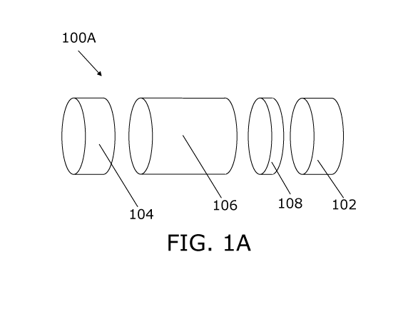
FIG 1A shows an exploded view drawing of a thermoelectric device 100A
according to an embodiment of the invention. The thermoelectric device 100A
comprises a layered structure comprising a first electrical connector 102, a
second
electrical connector pad 104, a first layer 106 in the form of a Zn45b3
pellet, and
a second layer 108, which second layer comprises zinc (Zn). In the shown
embodiment, the second layer 108 is embodied by a foil comprising Zn.
FIG 1B shows an exploded view drawing of another thermoelectric device 100B
which is similar to the thermoelectric device shown in FIG 1A, except that
third
layer 110 embodied by an other foil, which other foil comprises zinc (Zn), is
placed between the second electrical connector 104 and the first layer 106
embodied by a Zn4Sb3 pellet.
FIGS 2-3 show schematics where speculations relating to the underlying
principles
are illustrated.
FIG 2A shows a schematic showing a thermoelectric device 200 during a period
where a voltage is induced. The figure shows first electrical connector 202,
second
electrical connector 204, and first layer 206 embodied by a layer of Zn4Sb3.
Furthermore shown are Zn2+ ions, depicted as triangles 210. In the situation
shown, a non-zero voltage is induced across the first layer 206 and the first
CA 02813465 2013-04-03
WO 2012/045312 22 PCT/DK2011/050377
electrical connector 202 acts as anode whereas the second electrical connector
204 acts as cathode. In the present context, anode is used as generally
understood in the art, and defined as an electrical connector where oxidation
takes place. Similarly, 'cathode' is used as generally understood in the art
and
defined as an electrical connector where reduction takes place. The Zn2+ ions
210
are shown moving, by means of electromigration, from the anode towards the
cathode.
FIG 2B shows the same thermoelectric device 200 as in FIG 2A in a situation
after
a voltage has been induced across the first layer 206A-B for a period of time.
Due
to the electromigration of the Zn2+ ions, the first layer now has both a Zn
rich
region 206A and a Zn poor region 206B. The Zn poor regions may be termed
depletion zones.
FIG 3A shows a schematic showing a thermoelectric device 300, according to an
embodiment of the invention, during a period where voltage is induced. The
figure
shows first electrical connector 302, second electrical connector 304, second
layer
308 comprising Zn, and first layer 306 being a Zn4Sb3 element. Furthermore
shown are Zn2+ ions, depicted as triangles 310. In the situation shown a non-
zero voltage is induced across the Zn4Sb3 element 306 and the first electrical
connector 302 acts as anode whereas the second electrical connector 304 acts
as
cathode. The Zn2+ ions 310 are shown moving, by means of electromigration,
from the anode towards the cathode. Furthermore shown, is a Zn2+ ion 312
which emanates from the second layer 308 and which also moves, by means of
electromigration, from the anode towards the cathode.
FIG 3B shows the same thermoelectric device 300 as in FIG 3A in a situation
after
a voltage has been induced across the Zn4Sb3 element for a period of time. Due
to the electromigration of the Zn2+ ions, the Zn2+ ions originally located
within
the first layer 306 now has been relocated. However, due to the Zn2+ ions
emanating from the second layer 308 during the period where a non-zero voltage
is applied, there are substantially no depletion zones where the Zn content
has
dropped substantially.
CA 02813465 2013-04-03
WO 2012/045312 23 PCT/DK2011/050377
FIGS 4-5 and FIGS 7-8 show spatial distribution of Seebeck Coefficient for
different thermoelectric legs in different situations. In each scan, three
layers are
visible in. Two black layers corresponding to first and second electrical
connector,
which are here Cu electrodes (see also Fig 6B), and in the middle the first
layer
comprising Zn4Sb3. In some scans, a second layer and/or a third layer
comprising
zinc, such as a Zn foil, is present and placed, respectively, between the
first or
second electrical connector and the first layer, but this is not visible in
the scans.
In FIGS 4-5 and FIGS 7-10 the first layer comprises Zn4Sb3 thermoelectric
material, with or without 1 mol% Mg doping. The protocol for preparing this
material includes thermal quenching in analogy to the prior art quench method,
which is described in W02006/128467A2 which is hereby included as reference in
its entirety. In particular, reference is made to examples 1 and 2 in
W02006/128467A2.
FIG 4 shows spatial distribution of Seebeck Coefficient for different
thermoelectric
legs after preparation. What can be seen in the false colour diagram is a cut-
through sectional view through the centre of a first layer, in the form of a
Zn4Sb3
pellet, where the first and second electrical connectors, in the form of
copper (Cu)
rods, are placed along the upper- and lower side of the first layer,
respectively. In
FIG 4A-B, the electrical connector functioning as anode is placed along the
bottom
side 401A-B, respectively, and the electrical connector functioning as cathode
is
placed along the upper side 403A-B, respectively. The surface of the interface
was
grinded before performing the scans for obtaining the Seebeck Coefficients.
The
preparation of the pellet comprises placing first layer between Cu plates in a
pressing die, perform a sintering press. Or in other words, the preparation of
the
pellet comprises placing first layer between Cu plates in a pressing die, and
performing a sintering press. Specific condition may be given by a temperature
of
350 degree Celsius, a pressure of 25 MPa or 50 MPa, and the period for
pressing
given by 6 minutes. During preparation a current of the order of 1 kilo ampere
is
passed through the first layer from one Cu plate to the other Cu plate. A
Seebeck
Microprobe is used for measuring the spatial resolution of the Seebeck
coefficient
S in the sample which is a measure for the homogeneity or phase purity. The
Seebeck Microprobe is well known in the art and described in "Potential-
Seebeck-
Microprobe PSM: Measuring the Spatial Resolution of the Seebeck Coefficient
and
CA 02813465 2013-04-03
WO 2012/045312 24 PCT/DK2011/050377
the Electric Potential" by D. Platzek, G. Karpinski, C. Stiewe, P. Ziolkowski,
C.
Drasar, and E. Mueller, Proceeding of the 24th International Conference on
Thermoelectrics ICT, Clemson (USA) 2005, p. 13, which is hereby incorporated
by
reference in its entirety. Potential-Seebeck-Microprobe (PSM) is
interchangeably
referred to as Seebeck Microprobe.
FIG 4A shows the degradation of Zn45b3 in a thermoelectric device without a
second layer comprising Zn inserted between the Cu plate acting as anode and
the Zn45b3 pellet, after treating with a current of kilo ampere at 350 degree
Celsius during pressing. The Seebeck-coefficient changes from the for Zn45b3
typical 100 microvolt/Kelvin range to the value range of 300 microvolt/Kelvin
typical for ZnSb. Regions with relatively high Seebeck coefficients, such as
the
region indicated by the arrow, may be taken as a sign degradation already
during
preparation. The scale in FIG 4A and FIG 4B spans 0-200 microvolt/Kelvin.
FIG 4B shows the spatial distribution of the Seebeck coefficient S of a
thermoelectric device with a second layer, comprising Zn inserted between the
Cu
plate acting as anode and the Zn45b3 pellet, which thermoelectric device has
been shown treated under the same conditions as the thermoelectric device
shown in FIG 4A. Only Seebeck coefficients around the values typical for
Zn45b3,
i.e., around 100 microvolt/Kelvin range, can be observed.
FIG 5 shows spatial distribution of Seebeck Coefficient for different
thermoelectric
devices after preparation, as in FIG 4, except that the Zn45b3 material in FIG
5
have been doped with Magnesium (Mg) in a total amount of 1 mol% in relation to
the Zn atoms of Zn45b3, i.e. corresponding to Mg0.04, Zn3.96, 5b3. FIG 5A
reveals degradation already during preparation in the thermoelectric device
without the second layer inserted between anode and Zn45b3 pellet, which can
be
observed where the upper half of the pellet shows relatively high Seebeck
coefficient values, e.g., as indicated by the thick arrow 505. No degradation
can
be observed in FIG 5B where the thermoelectric device comprises a second layer
comprising Zn inserted between the first electrical connector embodied by a Cu
plate acting as anode and the first layer in the form of a Zn45b3 pellet. In
FIG 5A-
B, the electrical connector functioning as anode is placed along the bottom
side
501A-B, respectively, and the electrical connector functioning as cathode is
placed
CA 02813465 2013-04-03
WO 2012/045312 25 PCT/DK2011/050377
along the upper side 503A-B, respectively. In FIGS 5A-B, the scale spans 0-300
microvolt/Kelvin. In the examples of FIG 4B and FIG 5B, the second layer is
embodied by a foil comprising 99.9 wt% Zn. In this case the foil had a
thickness
of 100 micrometer. If the thickness of the first layer is lower, e.g., in the
range of
100 micrometer it may be advantageous to keep the foil in the range of, e.g.,
10
micrometer.
FIG 6A shows an experimental setup for long term testing, which setup
comprises
a heater and contact block 620A, a sample 622A, a contact block 624A, and
thermal- and electrical insulation 626A. The heater and contact block 620A and
the contact block 624A are connected electrically both via a measurement probe
628 for measuring voltage-current (U/I) characteristics, and via a current
source
630. During the long term tests the current source 628 delivers a DC current
of
10 ampere. The long term tests are conducted in ambient air, and the samples
are not sealed. In the present configuration, with the "+" wire leading to the
heater and contact block 620A, and the "-" wire leading to the contact block
624A,
the cathode side will be the same side as the side of the contact block 624A
and
the anode side will be the same as the side of the heater and contact block
620A.
Results from the long term tests are shown in FIGS 7-8.
FIG 6B is a photograph showing a thermoelectric device 600B comprising a
layered structure comprising a first layer 606B, being a Zn4Sb3 pellet, and
first
and second electrical connectors 602B, 604B embodied by Cu electrodes.
FIG 7 shows spatial distribution of Seebeck coefficient during long term
testing at
200 deg Celsius of a sample doped with Magnesium (Mg) in a total amount of 1
mol% in relation to the Zn atoms of Zn45b3, i.e. corresponding to Mg0.04,
Zn3.96, 5b3. The scans from left to right are measured after respectively 0,
500,
800, 1000 and 1500 minutes where the sample was exposed to a current of 10
ampere flowing through the sample and where the sample was held at 200 deg
Celcius in ambient atmosphere, i.e., exposed to atmospheric air. It is
observed
that no substantial degradation occurs. In FIG 7 the orientation is so that
the
electrical connector functioning as anode is placed along the right hand side
and
the electrical connector functioning as cathode is placed along the left hand
side.
CA 02813465 2013-04-03
WO 2012/045312 26 PCT/DK2011/050377
The left- and right hand side are the long edges. In FIG 7, the scale spans 0-
200
microvolt/Kelvin.
FIG 8 shows spatial distribution of Seebeck coefficient during long term
testing at
285 deg Celsius of a sample doped with Magnesium (Mg) in a total amount of 1
mol% in relation to the Zn atoms of Zn45b3, i.e. corresponding to Mg0.04,
Zn3.96, 5b3. The scans from left to right are measured after respectively 0,
200,
500 minutes where the sample was exposed to a current of 10 ampere flowing
through the sample and where the sample was held at 285 deg Celcius in ambient
atmosphere, i.e., exposed to atmospheric air. It is observed that no
substantial
degradation occurs. After 500 minutes small regions exhibiting relatively high
Seebeck coefficients can be seen as indicated by the arrow. This may be
interpreted as onset of degradation. As in FIG 7, the orientation is so that
the
electrical connector functioning as anode is placed along the right hand side
and
the electrical connector functioning as cathode is placed along the left hand
side.
The left- and right hand side are the long edges. In FIG 8, the scale spans 0-
200
microvolt/Kelvin. The pixeling in FIG 7 is somewhat noise, particularly in the
scans
corresponding to 1000 and 1500 minutes. This is interpreted as experimental,
noise leading to erroneous measurement points, i.e., the noise values are not
related to particularly high or low Seebeck coefficients.
In FIGS 7-8 both a second layer and a third layer is present, where both
second-
and third layer is embodied by a foil of 99.9 wt% Zn. Thus, a foil comprising
Zn is
placed between both electrical connectors, i.e., anode and cathode, and the
first
layer being a pellet of compressed Zn4Sb3 powder. The first and second
electrical
connectors are embodied by Cu rods. In an alternative embodiment, the first
and
second electrical connectors may also be embodied by compressed material,
which compressed material is highly conductive and capable of withstanding the
temperatures of preparation and use.
In a particular embodiment, the first and/or second connectors are made by
compressed powder, such as Cu powder. In another particular embodiment, the
first and/or second connector are realized by having powder, such as Cu
powder,
placed adjacent to the first layer or the second layer or the third layer and
performing a pressing step, such as a sintering step, so as to both compress
the
CA 02813465 2013-04-03
WO 2012/045312 27 PCT/DK2011/050377
powder into a solid element, being the first and/or second connector, and
adjoining the first and/or second connector to the first, second and/or third
layer.
An estimate of the Mean Time Between Failures (MTBT) may be given, by
calculating the ampere-hour (Ah) and relating this to a relevant current. In
the
given case, the inner resistance was measured by observing a voltage of 0.6 V
at
A corresponding to 0.06 Ohm. The average Seebeck coefficient is
approximately 150 microvolt/Kelvin. A temperature difference of 200 Kelvin
thus
corresponds to 30 mV. In use as a thermoelectric device, a load resistance
with
10 the same magnitude as the inner resistance of the thermoelectric leg is
coupled in
series with the thermoelectric leg. The current through the leg during
practical use
consequently amounts to 30 mV/K / (2*0.06 Ohm) = 0.25 A. As a result, the
MTBF can be estimated by equating the ampere hour (Ah) for the conditions
during test and use, and obtain
MTBT = 1500 minutes * 10 A / 0.25 A = 60000 minutes = 1000 hours
FIG 9A-B shows respectively voltage-current characteristics (U[V] vs. I[A])
and
electrical conductivity (sigma[1/(Omega meter)] vs. I[A]) as a function of
current
for Zn45b3 pellets without second or third layer 940, with second layer placed
between the first layer and the first electrical connector where the first
electrical
connector is functioning as anode 942, with second layer placed between the
first
layer and the first electrical connector where the first electrical connector
is
functioning as cathode 944 and both second and third layer comprising zinc
946.
FIG 10A-B similar kinds of datasets as in FIG 9, however, FIG 10 shows
datasets
measured on Zn45b3 pellets which have been doped with Magnesium (Mg) in a
total amount of 1 mol% in relation to the Zn atoms of Zn45b3, i.e.
corresponding
to Mg0.04, Zn3.96, 5b3. Thus FIG 10A-B shows in a similar manner to FIG 9
respectively voltage-current (U[V] vs. I[A]) and electrical conductivity
(sigma[1/(Omega meter)] vs. I[A]) as a function of current for Mg doped Zn45b3
pellets without second or third layer 1040, with second layer placed between
the
first layer and the first electrical connector where the first electrical
connector is
functioning as anode 1042 and both second and third layer comprising zinc
1046.
It is noted that the measuring point corresponding to a current of 2 ampere
for
CA 02813465 2013-04-03
WO 2012/045312 28 PCT/DK2011/050377
the curves denoted with reference signs 1042 and 1046 may be erroneous in FIGS
10A-B.
In FIGS 9-10, each second or third layer is embodied by a foil of 99.9 wt% Zn.
It
can be seen from FIGS 9-10 that the electrical conductivity is significantly
increased compared to samples without Zn foil. Furthermore, mechanical
stability
of the complete thermoelectric leg including first and second electrical
connectors
is significantly increased compared to samples without the second layer, such
as a
Zn foil. The increased mechanical stability of the thermoelectrical legs
comprising
a second layer, such as a foil comprising Zn, is evident as those
thermoelectric
legs are less prone to fracturing compared to thermoelectric legs without the
second layer. Without the increased mechanical stability, the thermoelectrical
legs
may fracture during simple handling, whereas the increased mechanical
stability
may ensure that samples can withstand simple handling, such as moving and
general handling by hand.
In an exemplary embodiments, there is provided a thermoelectric device (100A)
comprising a layered structure comprising
- a first layer (106), the first layer comprising a material having the
stoichiometric
formula Zn45b3,
- a first electrical connector (102),
- a second electrical connector (104), and
- a second layer (108) being different from the first layer (106), the
second layer
comprising Zn,
the first layer being placed between the first and second electrical
connector, and
the second layer being placed between the first layer and the first electrical
connector.
In another exemplary embodiments, there is provided a method of manufacturing
a thermoelectric device according to any of the preceding claims, the method
comprising
- providing the first layer,
- providing the first and second electrical connectors,
- providing the second layer, and
CA 02813465 2013-04-03
WO 2012/045312 29 PCT/DK2011/050377
- arranging the first layer between the first and second electrical connectors
with
the second layer being arranged between the first layer and the first
electrical
connector.
To sum up, the present invention relates to a thermoelectric device comprising
a
layered structure comprising a first layer, a first electrical connector, a
second
electrical connector, and a second layer being different from the first layer,
where
the first layer comprises a material having the stoichiometric formula Zn45b3
(zinc antimonide) and the second layer comprises Zn (zinc). The first layer is
being placed between the first and second electrical connector, and the second
layer is placed between the first layer and the first electrical connector. By
having
a second layer comprising Zn the negative effects of electromigration of Zn
may
be overcome, since Zn may emanate from the foil and refill Zn depleted regions
in
the first layer. In a particular embodiment the second layer is a foil. In
another
particular embodiment, the first layer is doped with an element such as
magnesium.
Although the present invention has been described in connection with the
specified embodiments, it should not be construed as being in any way limited
to
the presented examples. The scope of the present invention is set out by the
accompanying claim set. In the context of the claims, the terms "comprising"
or
"comprises" do not exclude other possible elements or steps. Also, the
mentioning
of references such as "a" or "an" etc. should not be construed as excluding a
plurality. The use of reference signs in the claims with respect to elements
indicated in the figures shall also not be construed as limiting the scope of
the
invention. Furthermore, individual features mentioned in different claims, may
possibly be advantageously combined, and the mentioning of these features in
different claims does not exclude that a combination of features is not
possible
and advantageous.