Note: Descriptions are shown in the official language in which they were submitted.
CA 02813829 2013-04-05
WO 2012/049473 PCT/GB2011/051837
1
A LOOP ANTENNA FOR MOBILE HANDSET AND OTHER APPLICATIONS
[0001] This invention relates to a loop antenna for mobile handset and other
applications,
and in particular to a loop antenna that is able to operate in more than one
frequency band.
BACKGROUND
[0002] The industrial design of modern mobile phones leaves little printed
circuit board (PCB)
area for the antenna and often the antenna must be very low profile because of
the increasing
demand for slimline phones. At the same time the number of frequency bands
that the
antenna is expected to operate over is increasing.
[0003] When multiple radio protocols are used on a single mobile phone
platform, the first
problem is to decide whether a single wideband antenna should be used or
whether multiple
narrower band antennas would be more appropriate. Designing a mobile phone
with a single
wideband antenna involves problems not only with obtaining sufficient
bandwidth to cover all
the necessary bands but also with the difficulties associated with the
insertion loss, cost,
bandwidth and size of the circuits needed to diplex the signals together. On
the other hand,
multiple narrow-band antenna solutions are associated with problems dominated
by the
coupling between them and the difficulties of finding sufficient real estate
for them on the
handset. Generally, these multiple antenna problems are harder to solve than
the wide-band
single antenna problems.
[0004] Most mobile phones generally make use of monopole antennas or PIFAs
(Planar
Inverted F Antennas). Monopoles work most efficiently in areas free from
the PCB
groundplane or other conductive surfaces. In contrast, PIFAs will work well
close to conductive
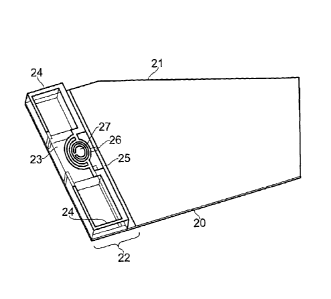
surfaces. Considerable research effort goes into making monopoles and PIFAs
operate as
broadband antennas so as to avoid the issues associated with multiple
antennas.
[0005] One way to increase bandwidth in an electrically small antenna is to
use multi-moding.
In the lowest bands, odd resonant modes may be created which may be variously
designated
as 'unbalanced modes', 'differential modes' or 'monopole-like'. At higher
frequencies both
even and odd resonant modes may created. Even modes may be variously
designated as
'balanced modes', 'common modes' or 'dipole-like'.
[0006] Loop antennas are well-understood and have been used in mobile phones
before. An
example is US 2008/0291100 which describes a single band grounded loop
radiating in the
low band together with a parasitic grounded monopole radiating in the high
band. A further
example is WO 2006/049382 which discloses a symmetrical loop antenna structure
that has
CA 02813829 2013-04-05
WO 2012/049473 PCT/GB2011/051837
2
been reduced in size by stacking the loop vertically. A broadband
characteristic has been
obtained in the high frequency band by attaching a stub to the top patch of
the antenna. This
arrangement creates a multi-moding antenna useful in wireless communication
fields.
[0007] The idea of multi-moding an antenna is also not new. An example of good
design
practice here is the Motorola Folded Inverted Conformal Antenna (FICA), which
excites
resonances in a structure that exhibits odd and even resonant modes [Di Nallo,
C. and
Faraone, A.: "Multiband internal antenna for mobile phones", Electronics
Letters 28th April
2005 Vol. 41 No. 9]. Two modes are described as being synthesised for the high
band: a
'differential mode', featuring opposite phased currents on the FICA arms and
transverse
currents on the PCB ground and a 'slot mode', which is a higher order common
mode,
featuring a strong excitation of the FICA slot. The combination of modes can
be used to
produce a wide, continuous radiating band. However, the FICA structure
referred to is a
variation of the PIFA and the Nallo and Faraone paper does not teach multi-
moding of loop
antennas.
BRIEF SUMMARY OF THE DISCLOSURE
[0008] Embodiments of the present invention make use of a loop antenna design
that has
been multi-moded. Embodiments of the present invention are useful in mobile
phone
handsets, and may also be used in mobile modem devices, for example USB
dongles and the
like for allowing a laptop computer to communicate with the internet by way of
a mobile
network.
[0009] According to a first aspect of the present invention there is provided
a loop antenna
comprising a dielectric substrate having first and second opposed surfaces and
a conductive
track formed on the substrate, wherein there is provided a feed point and a
grounding point
adjacent to each other on the first surface of the substrate, with the
conductive track extending
in generally opposite directions from the feed point and grounding point
respectively, then
extending towards an edge of the dielectric substrate, then passing to the
second surface of
the dielectric substrate and then passing across the second surface of the
dielectric substrate
along a path generally following the path taken on the first surface of the
dielectric substrate,
before connecting to respective sides of a conductive arrangement formed on
the second
surface of the dielectric substrate that extends into a central part of a loop
formed by the
conductive track on the second surface of the dielectric substrate, wherein
the conductive
arrangement comprises both inductive and capacitive elements.
[0010] The conductive arrangement can be considered to be electrically
complex, in that it
includes both inductive and capacitive elements. The inductive and capacitive
elements may
CA 02813829 2013-04-05
WO 2012/049473 PCT/GB2011/051837
3
be lumped components (e.g. as discrete surface mount inductors or capacitors),
but in
preferred embodiments they are formed or printed as distributed components,
for example as
regions of appropriately shaped conductive track on or in the second surface
of the substrate.
[0011] This arrangement differs from that disclosed in WO 2006/049382 in that
the latter
describes a folded loop antenna having a stub on the top surface that expands
the bandwidth
of the high frequency band of the antenna. WO 2006/049382 makes clear that
'the stub is a
line that is additionally connected to a transmission line for the purpose of
frequency tuning or
broadband characteristic'. The stub is a 'shunt stub connected in parallel to
the top patch and
is the open stub whose length is smaller than X14'. It is also made clear in
WO 2006/049382
that 'when the length [stub] L is smaller than k14, the open stub acts as a
capacitor'. In the
present invention, the antenna includes a series complex structure at, or
near, a centre of the
loop instead of the simple capacitive shunt stub described in WO 2006/049382.
[0012] In both the lumped and the distributed cases, the conductive
arrangement of
embodiments of the present invention is smaller than the shunt stub described
in WO
2006/049382 and allows the overall antenna structure to be made more compact.
A further
advantage of this structure is that it allows the impedance bandwidth of the
high band to be
tuned without any deleterious effects on the low band. This allows the high
band match to be
much improved.
[0013] Inductive and capacitive elements may be provided in the central region
of the loop on
the second surface of the substrate by forming the conductive tracks on the
second surface of
the substrate to define at least one slot, for example by running one track
into the central
region and then generally parallel to the other track but not galvanically
contacting the other
track.
[0014] It will be appreciated that the conductive track forms a loop with two
arms, the loop
starting at the feed point and terminating at the grounding point. The two
arms of the loop
initially extend away from each other starting at the feed point and grounding
point
respectively, before extending towards the edge of the dielectric substrate.
In preferred
embodiments, the arms are collinear when initially extending from the feed and
grounding
points, and generally or substantially parallel when extending towards the
edge of the dielectric
substrate, although other configurations (for example diverging or converging
towards the
edge of the dielectric substrate) are not excluded.
[0015] In particularly preferred embodiments, the arms of the loop extend
towards each other
along or close to the edge of the dielectric substrate. The arms may extend so
that they come
close to each other (for example as close as or closer than the distance
between the feed
CA 02813829 2013-04-05
WO 2012/049473 PCT/GB2011/051837
4
point and the grounding point), or less close to each other. In other
embodiments, one arm of
the loop may extend along or close to the edge of the substrate while the
other does not. In
other embodiments, it is conceivable that the arms do not extend towards each
other.
[0016] The conductive track on the first surface of the dielectric substrate
may pass through
.. the dielectric substrate to the second surface by means of vias or holes.
Alternatively, the
conductive track may pass over the edge of the dielectric substrate from one
surface to the
other. It will be appreciated that the conductive track passes from one side
of the substrate to
the other side of the substrate at two locations. Both of these passages may
be through vias
or holes, or both may be over the edge of the substrate, or one may be through
a via or hole
and the other may be over the edge.
[0017] The loop formed by the conductive track and the loading plate may be
symmetrical in
a mirror plane perpendicular to a plane of the dielectric substrate and
passing between the
feed point and the grounding point to the edge of the substrate. In addition,
the conductive
track, notwithstanding the loading plate, may be generally symmetrical about a
mirror plane
defined between the first and second surfaces of the substrate. However, other
embodiments
may not be symmetrical in these planes. Non-symmetrical embodiments may be
useful in
creating an unbalanced loop which may improve bandwidth, especially in higher
bands.
However, a consequence of this is that the antenna becomes less resistant to
detuning when
there is a change in the shape or size of the groundplane.
[0018] Advantageously, the conductive track may be provided with one or more
spurs
extending from the loop generally defined by the conductive track. The one or
more spurs
may extend into the loop, or out of the loop, or both. The additional spur or
spurs act as
radiating monopoles and contribute additional resonances in the spectrum,
thereby increasing
the bandwidth of the antenna.
[0019] Alternatively or in addition, there may be provided at least one
parasitic radiating
element. This may be formed on the first or second surface of the substrate,
or on a different
substrate (for example a motherboard on which the antenna and its substrate is
mounted).
The parasitic radiating element is a conductive element that may be grounded
(connected to a
groundplane) or ungrounded. By providing a parasitic radiating element, it is
possible to add a
further resonance that may be used for an additional radio protocol, for
example Bluetoothe or
GPS (Global Positioning System) operation.
[0020] In some embodiments, antennas of the present invention may operate in
at least four,
and preferably at least five different frequency bands.
[0021] According to a second aspect of the present invention there is provided
a parasitic
CA 02813829 2013-04-05
WO 2012/049473 PCT/GB2011/051837
loop antenna comprising a dielectric substrate having first and second opposed
surfaces and a
conductive track formed on the substrate, wherein there is provided a first
ground point and a
second ground point adjacent to each other on the first surface of the
substrate, with the
conductive track extending in generally opposite directions from the first and
second ground
5 .. points respectively, then extending towards an edge of the dielectric
substrate, then passing to
the second surface of the dielectric substrate and then passing across the
second surface of
the dielectric substrate along a path generally following the path taken on
the first surface of
the dielectric substrate, before connecting at a conductive loading plate
formed on the second
surface of the dielectric substrate that extends into a central part of a loop
formed by the
conductive track on the second surface of the dielectric substrate, and
wherein there is further
provided a separate, directly driven antenna configured to excite the
parasitic loop antenna.
[0022] The separate driven antenna may take the form of a smaller loop antenna
located on
adjacent a portion of the conductive track extending from the first ground
point, the second
loop antenna having a feed point and a ground point and configured to drive
the parasitic loop
antenna by inductively coupling therewith. The drive antenna may be formed on
a
motherboard to which the parasitic loop antenna and its substrate is attached.
[0023] Alternatively, the separate drive antenna may take the form of a
monopole antenna,
preferably a short monopole, located and configured so as to drive the
parasitic loop antenna
by capacitively coupling therewith. The monopole may be formed on a reverse
side of a
motherboard to which the parasitic loop antenna and its substrate is attached.
[0024] WO 2006/049382 describes a classical half-loop antenna that has been
compacted
by means of a vertical stack structure. Typically a half-loop antenna
comprises a conductive
element that is fed at one end and grounded at the other. The second aspect of
the present
invention is a radiating loop antenna that is grounded at both ends and which
is therefore
parasitic. This parasitic loop antenna is excited by a separate driven
antenna, generally
smaller than the parasitic loop antenna. The driven or driving antenna may be
configured to
radiate at a higher frequency of interest, such as one of the WiFi frequency
bands.
[0025] The loading plate may be generally rectangular in shape, or may have
other shapes,
for example taking a triangular form. The loading plate may additionally be
provided with arms
.. or spurs or other extensions extending from a main part of the loading
plate. The loading plate
is formed as a conductive plate on the second surface of the substrate,
parallel to the
substrate as a whole. One edge of the loading plate may follow, on the second
surface, a line
formed between the feed point and the grounding point on the first surface. An
opposed edge
of the loading plate may be located generally in the centre of the loop formed
by the
.. conductive track on the second surface.
CA 02813829 2013-04-05
WO 2012/049473 PCT/GB2011/051837
6
[0026] According to a third aspect of the present invention there is provided
a parasitic loop
antenna comprising a dielectric substrate having first and second opposed
surfaces and a
conductive track formed on the substrate, wherein there is provided a first
ground point and a
second ground point adjacent to each other on the first surface of the
substrate, with the
conductive track extending in generally opposite directions from the first and
second ground
points respectively, then extending towards an edge of the dielectric
substrate, then passing to
the second surface of the dielectric substrate and then passing across the
second surface of
the dielectric substrate along a path generally following the path taken on
the first surface of
the dielectric substrate, before connecting to respective sides of a
conductive arrangement
.. formed on the second surface of the dielectric substrate that extends into
a central part of a
loop formed by the conductive track on the second surface of the dielectric
substrate, wherein
the conductive arrangement comprises both inductive and capacitive elements,
and wherein
there is further provided a separate, directly driven antenna configured to
excite the parasitic
loop antenna.
[0027] The third aspect of the present invention combines the parasitic
excitation mechanism
of the second aspect with the electrically complex conductive arrangement of
the first aspect.
[0028] In a fourth aspect, which may be combined with any of the first to
third aspect, the
loop antenna, instead of being directly grounded, is grounded though a complex
load selected
from the list comprising: least one inductor, at least one capacitor; at least
one length of
transmission line; and any combination of these in series or in parallel.
[0029] Furthermore, the grounding point of the loop antenna may be switched
between
several different complex loads so as to enable the antenna to cover different
frequency
bands.
[0030] The various embodiments of the present invention already described may
be
configured as either surface mount (SMT) components that may be reflowed onto
a ground-
plane free area of a main PCB, or as elevated structures that work over a
groundplane.
[0031] It has further been found that removing substrate material in the
region of high electric
field strength may be used to reduce losses. For example, a central notch may
be cut into the
substrate material of the loop antenna where the E-field is highest resulting
in improved
performance in the high frequency band.
[0032] For the antenna having a complex central loading structure, it has been
found
advantageous to make two cut-outs either side of the centre line. Again the
efficiency benefits
are mainly in the high frequency band.
[0033] The loop antenna may be arranged so as to leave a central area free for
a cut-out
CA 02813829 2016-09-28
51331-1451
7
right through part of the antenna substrate. The objective here is not so much
to reduce
losses but rather to create a volume where a micro-USB connector or the like
may be placed.
It is often desirable to locate the antenna in the same place as connectors,
for example at the
bottom of a mobile phone handset.
[0034] In a further embodiment it has found that short capacitive or inductive
stubs may be
attached to a driven or parasitic loop antenna to improve the bandwidth,
impedance match
and/or efficiency. The idea of using a single shunt capacitive stubs has been
previously been
disclosed in GB0912368.8 and WO 2006/049382, however it has been found
particularly
advantageous to use several such stubs, as part of the central complex load.
The stubs may
also be used advantageously when connected to other parts of the loop
structure, as already
described in the present Applicant's co-pending UK patent application no
GB0912368.8 .
[0035] It has been found that embodiments of the present invention may be used
in
combination with an electrically small FM radio antenna tuned to band 88-108
MHz with one
antenna disposed each side of the main PCB, i.e. one on the top surface and
one directly
below it on the undersurface. It is usually a problem to use two antennas so
closely spaced
because of the coupling between them but it has been found that the loop
design of
embodiments of the present invention and the nature of the FM antenna (itself
a type of loop)
Is such that very good isolation may exist between them.
[0036] Electrically small monopoles and PIFAs are characterised by a high
reactive
impedance that is capacitive in nature in the same way that a short open-ended
stub on a
transmission line is capacitive. Most loop antenna configurations have a low
reactive
impedance that is inductive in nature in the same way that a short-circuited
stub on a
transmission line is inductive. There are difficulties in matching both these
types of antenna to
a 50 ohm radio system. Like monopoles and PIFAs, loop antennas can be short
circuited to
ground so as to be unbalanced or monopole-like. In this case the loop may act
as a half-loop
and 'see' its image in the groundplane. Alternatively a loop antenna may be a
complete loop
with balanced modes requiring no groundplane for operation.
[0037] Embodiments of the present invention comprise a grounded loop that is
driven in both
odd and even modes so as to operate over a very wide bandwidth. The operation
of the
antenna will be explained in more detail below.
81773940
7a
[0037a] According to one aspect of the present invention, there is provided a
loop
antenna comprising: a dielectric substrate with first and second opposed
surfaces; a
feed point and a grounding point adjacent to each other on the first surface
of the
dielectric substrate; a conductive track formed on the dielectric substrate
and
including ends that extend in generally opposite directions away from the feed
point
and grounding point, respectively, toward opposite edges of the dielectric
substrate,
over the opposite edges and to the second surface of the dielectric substrate,
across
the second surface of the dielectric substrate and along a path generally
following
the path taken on the first surface of the dielectric substrate, and wherein
the ends
connect to respective sides of a conductive arrangement formed on the second
surface of the dielectric substrate that extends into a central part of a loop
formed by
the conductive track on the second surface of the dielectric substrate,
wherein the
conductive arrangement comprises both inductive and capacitive elements.
BRIEF DESCRIPTION OF THE DRAWINGS
[0038] Embodiments of the invention are further described hereinafter with
reference
to the accompanying drawings, in which:
CA 2813829 2018-03-21
CA 02813829 2013-04-05
WO 2012/049473 PCT/GB2011/051837
8
FIGURE 1 is a schematic outline of the structure of a prior art vertically
stacked loop antenna;
FIGURE 2 shows an embodiment of the present invention with an electrically
complex central
load;
FIGURE 3 shows an alternative embodiment in which an electrically complex
central load is
formed by a slot;
FIGURE 4 shows an arrangement in which a separate feeding loop antenna is used
to excite
the main loop antenna by coupling inductively therewith;
FIGURE 5 is a plot showing the performance of the embodiment of Figure 4, both
before and
after matching;
FIGURE 6 is a schematic circuit diagram showing how embodiments of the present
invention
may be grounded through different loads;
FIGURE 7 shows an arrangement in which a loop antenna is vertically compacted
across
opposed sides of a dielectric substrate, and in which a central notch or cut-
out is formed in the
dielectric substrate;
FIGURE 8 shows a variation of the embodiment of Figure 2, in which portions of
the substrate
are cut out or removed on either side of the central complex load;
FIGURES 9 and 10 show a variation in which the loop antenna is arranged and
the dielectric
substrate cut through in such a way as to accommodate a connector, such as a
micro USB
connector;
FIGURE 11 shows a variation in which short capacitive or inductive stubs are
attached to the
loop antenna;
FIGURE 12 shows an embodiment of the present invention combined with an FM
radio
antenna; and
FIGURE 13 is a plot showing coupling between the loop antenna and FM radio
antenna of the
embodiment of Figure 12.
CA 02813829 2013-04-05
WO 2012/049473 PCT/GB2011/051837
9
DETAILED DESCRIPTION
[0039] Figure 1 shows in schematic form a prior art loop antenna generally
similar to that
disclosed in WO 2006/049382. The dielectric substrate, which will typically be
a slab of FR4
PCB substrate material, is not shown in Figure 1 for the sake of clarity. The
antenna 1
comprises a loop formed of a conductive track 2 extending between a feed point
3 and a
grounding point 4 both located adjacent to each other on a first surface (in
this case an
underside) of the substrate. The conductive track 2 extends in generally
opposite directions 5,
6 from the feed point 3 and grounding point 4 respectively, then extends 7, 8
towards an edge
of the dielectric substrate, then passes 9, 10 along the edge of the
dielectric substrate before
passing 11, 12 to the second surface of the dielectric substrate. The
conductive track 2 then
passes across the second surface of the dielectric substrate along a path
generally following
the path taken on the first surface of the dielectric substrate, before
connecting at a conductive
loading plate 13 formed on the second surface of the dielectric substrate that
extends into a
central part 14 of a loop 15 formed by the conductive track 2 on the second
surface of the
dielectric substrate.
[0040] It can be seen that the conductive track 2 is folded so as to cover the
upper and lower
layers of the slab of FR4 substrate material. The feed point 3 and grounding
point 4 are on
the lower surface and may be interchanged if the groundplane is symmetrical
through the
same axis of symmetry as the antenna 1 as a whole. In other words, if the
antenna 1 is
symmetrical, then either terminal point 3, 4 may be used as the feed and the
other for
grounding. Generally, both feed point 3 and grounding point 4 will be on the
same surface of
the antenna substrate, since the motherboard on which the antenna 1 as a whole
will be
mounted can feed the points 3 and 4 from only one of its surfaces. However, it
is possible to
use holes or vias through the substrate so that feed tracks can be formed on
either surface
and still connect to the respective feed point 3 or grounding point 4. The
conductive loading
plate 13 is located on the upper surface of the antenna close to the
electrical centre of the loop
15.
[0041] Given that the greatest dimension of the loop 15 is 40mm, it can be
appreciated that
the conductive track 2 as a whole is approximately half a wavelength long in
the mobile
communications low band (824 ¨ 960MHz) where the wavelength is around 310-360
mm. In
this situation the input impedance of the loop is capacitive in nature and
leads to an increased
radiation resistance and a lower Q (a larger bandwidth) than is common for a
loop antenna.
The antenna thus works well in the low band and it is not too difficult to
match over required
CA 02813829 2013-04-05
WO 2012/049473 PCT/GB2011/051837
bandwidth. Because the antenna 1 is formed as a loop that is folded over onto
itself, its self-
capacitance helps to reduce the operating frequency in certain embodiments.
[0042] Figure 2 shows an improvement over the prior art antenna of Figure 1.
There is
shown a PCB substrate 20 including a conductive groundplane 21. The PCB
substrate 20 has
5 an edge portion 22 that is free of the groundplane 21 for mounting an
antenna structure 22 of
an embodiment of the present invention. The antenna structure 22 comprises a
dielectric
substrate 23 (for example FR4 or Duroid or the like) with first and second
opposed surfaces.
A conductive track 24 is formed (for example by way of printing) on the
substrate 23 having a
similar overall configuration to that shown in Figure 1, namely that of a
vertically-compacted
10 loop with a feed point 26 and a grounding point 25 adjacent to each
other on the first surface
of the substrate, with the conductive track 24 extending in generally opposite
directions from
the feed point 26 and grounding point 25 respectively, then extending towards
an edge of the
dielectric substrate 23, then passing to the second surface of the dielectric
substrate 23 and
then passing across the second surface of the dielectric substrate 23 along a
path generally
following the path taken on the first surface of the dielectric substrate 23.
The two ends of the
conductive track 24 on the second surface of the substrate 23 then connect to
respective sides
of a conductive arrangement 27 formed on the second surface of the dielectric
substrate 23
that extends into a central part of a loop formed by the conductive track 24
on the second
surface of the dielectric substrate 23, wherein the conductive arrangement 27
comprises both
inductive and capacitive elements. In comparison with the arrangement of
Figure 1, the high
band match is much improved.
[0043] Figure 3 shows a variation of the arrangement of Figure 2, with like
parts labelled as
for Figure 2. This embodiment provides an electrically complex (i.e. inductive
and capacitive)
load in the central region of the second surface of the substrate 23 by means
of a stub 28 and
slots 29, 30. This technique also adds inductance and capacitance near the
center of the
loop.
[0044] Figure 4 shows a variation (this time omitting the substrate 23 and top
half of the
antenna from the drawing for clarity) in which the main loop antenna defined
by the conductive
track 24 is connected at both terminals 25, 25' to ground 21. In other words,
the main loop
antenna is not directly driven by a feed 26 as in Figures 2 and 3. Instead,
the main loop
antenna is excited by a separate, smaller, driven loop antenna 33 formed on
the end 22 of the
PCB substrate 20 on which there is no groundplane 21, the driven loop antenna
33 having a
feed 31 and a ground 32 connection. The smaller, driven loop antenna 33 may be
configured
to radiate at a higher frequency of interest, such as one of the WiFi
frequency bands.
[0045] This inductively coupled feeding arrangement has many parameters that
may be
CA 02813829 2013-04-05
WO 2012/049473 PCT/GB2011/051837
11
varied in order to obtain optimum impedance matching. An example of the
performance of the
antenna, before and after matching, is shown in Figure 5. Lumped or tunable L
and C
elements may be added to the ground 32 of the small coupling loop 23 to adjust
impedance
response of the antenna as a whole.
[0046] In a variation of the inductive feeding of a parasitic loop antenna 33,
the parasitic
main loop may be fed capacitively by means of a short monopole on the
underside of the main
PCB substrate 20 coupling to a section of the antenna on the top side of the
main PCB 20.
This arrangement has been disclosed in a previous patent application, UK
patent application
No GB0914280.3 to the present applicant.
[0047] Instead of directly grounding the main loop antenna, it is sometimes
advantageous to
ground the antenna through a complex load comprising inductors, capacitors or
lengths of
transmission line or any combination of these in series or parallel.
Furthermore, the grounding
point of the antenna may be switched between several different complex loads
so as to enable
the antenna to cover different frequency bands as shown in Figure 6. Figure 6
shows the
grounding connection 25 and the groundplane 21 of the main PCB substrate 20.
The
grounding connection 25 connects to the groundplane 21 by way of a switch 34
that can
switch in different inductive and/or capacitive components 35 or 36, or
provide a direct
connection 37. In the example shown below, the complex grounding loads were
chosen so
that in switch position 1 the low band of the antenna covered the LTE band 700-
760 MHz; in
switch position 2, 750-800 MHz and in switch position 3, the GSM band 824-960
MHz.
[0048] It has been found that removing substrate 23 material in the region of
high electric
field strength may be used to reduce losses. In the example shown in Figure 7,
a central
notch 38 has been cut into the substrate material 23 where the E-field is
highest, resulting in
improved performance in the high frequency band.
[0049] Figure 8 shows a variation of the embodiment of Figure 2, where parts
of the
substrate 23 are cut out from the second surface on either side of the central
complex load 27.
In this example, the cut-outs are generally cuboidal in shape, although other
shapes and
volumes may be useful. The efficiency benefits are mainly in the high
frequency band.
[0050] Figures 9 and 10 show a variation in which the main loop antenna is
defined by the
track 24 and complex load 27 on the substrate 23 is arranged so as to leave a
central area 42
free for a cut-out 40 right through part of the antenna substrate 23. The
objective here is not
so much to reduce losses but rather to create a volume where a micro-USB
connector 41 or
similar may be located. It is often desirable to locate the antenna in the
same place as
connectors, for example at the bottom of a mobile phone handset.
CA 02813829 2013-04-05
WO 2012/049473 PCT/GB2011/051837
12
[0051] In a further embodiment it has found that short capacitive or inductive
stubs 43 may
be attached to a driven or parasitic loop antenna 24 to improve the bandwidth,
impedance
match and/or efficiency, as shown in Figure 11. It has been found particularly
advantageous
to use several such stubs 43, as part of the central complex load 27. The
stubs 43 may also
be used advantageously when connected to other parts of the loop structure 24.
Cut-outs 39
in the substrate 23 may also be provided to improve efficiency.
[0052] Figure 12 shows an embodiment of the present invention corresponding
generally to
that of Figures 9 and 10 in combination with an electrically small FM radio
antenna 44 tuned to
band 88-108 MHz and mounted on the reverse side of the main PCB 20 to the side
on which
the loop antenna 24 is mounted. In other words, one antenna is on the top
surface of the PCB
and the other is directly below it on the undersurface of the main PCB 20. It
is usually a
problem to use two antennas so closely spaced because of the coupling between
them but it
has been found that the loop design of embodiments of the present invention
and the nature
of the FM antenna (itself a type of loop) is such that very good isolation may
exist between
15 them.
[0053] Figure 13 shows that the coupling between the two antennas 24 and 44
(the lower
plot) is lower than ¨30 dB across the whole of the cellular band.
[0054] Throughout the description and claims of this specification, the words
"comprise" and
"contain" and variations of them mean "including but not limited to", and they
are not intended
20 to (and do not) exclude other moieties, additives, components, integers
or steps. Throughout
the description and claims of this specification, the singular encompasses the
plural unless the
context otherwise requires. In particular, where the indefinite article is
used, the specification
is to be understood as contemplating plurality as well as singularity, unless
the context
requires otherwise.
[0055] Features, integers, characteristics, compounds, chemical moieties or
groups
described in conjunction with a particular aspect, embodiment or example of
the invention are
to be understood to be applicable to any other aspect, embodiment or example
described
herein unless incompatible therewith. All of the features disclosed in this
specification
(including any accompanying claims, abstract and drawings), and/or all of the
steps of any
method or process so disclosed, may be combined in any combination, except
combinations
where at least some of such features and/or steps are mutually exclusive. The
invention is not
restricted to the details of any foregoing embodiments. The invention extends
to any novel
one, or any novel combination, of the features disclosed in this specification
(including any
accompanying claims, abstract and drawings), or to any novel one, or any novel
combination,
of the steps of any method or process so disclosed.
CA 02813829 2016-09-28
51331-1451
13
[0056] The reader's attention is directed to all papers and documents which
are filed
concurrently with or previous to this specification in connection with this
application and which
are open to public inspection with this specification.