Note: Descriptions are shown in the official language in which they were submitted.
CA 02814339 2013-04-30
WO 2012/063147 PCT/IB2011/054396
Circuit Visualization Using Flightlines
BACKGROUND
Technical Field
Various embodiments of the present invention relate to electronic circuitry,
and more
specifically, to tools for analyzing the interconnection between electronic
circuitry components.
Description of Related Art
Electronic circuitry consists primarily of elements and connections between
elements.
There is often a need to understand how a particular circuit operates based on
observation of the
circuit itself. This may be done by having engineers trace the various
circuitry connections one
by one, and organize the components based on their connections. The engineers
may arrive at a
plausible organization of the entire circuit in a reasonable amount of time
for circuits that are
simple with a relatively small number of components and connections. However,
as the number
of elements and connections grows, this traditional method becomes
increasingly difficult to use.
A modest digital circuit may contain tens of thousands of components, and at
least as many
connections between them. Some modern circuitry assemblies may have many
hundreds of
thousands of elements, and a comparable number of connections between the
elements. Tracing
connections one-by-one is not practical in these cases. It would take far too
much time to
understand anything more than a trivial circuit using this inefficient
conventional approach.
Conventional schematic editor tools are available on the market such as
Cadence's
Virtuoso Schematic Editor. However, the conventional schematic editor tools
are quite limited
in their ability to categorize, manipulate and display circuitry components.
What is needed is an
improved system for organizing and displaying unorganized circuitry
components.
BRIEF SUMMARY
In order to understand how a complicated circuit functions there is a need to
organize the
circuit in some manner. Various embodiments disclosed herein allow engineers
to visualize
connections between components in a faster and more efficient manner than can
be done using
conventional methods. The various embodiments display many connections at
once, with
information about the connections coded in a visual format directly on the
circuit under analysis.
According to at least some of the various embodiments a method of presenting a
display
of circuitry interconnections between components of a circuit is provided.
Flightline display
1
CA 02814339 2013-04-30
WO 2012/063147 PCT/1B2011/054396
settings are obtained, for example, by retrieving them from memory. The
flightline display
settings control the appearance characteristics of flightlines which represent
the connections
between predefined components of the circuit. The flightline display settings
may be
reconfigurable by a user of the system. The system displays a local component
of the circuit,
typically indicated by a user, and any foreign components connected to the
local component.
The system also displays flightlines representing the connections between the
local component
and foreign components. The appearance characteristics of the flightline are
controlled by the
flightline display settings, which may be user specified.
BRIEF DESCRIPTION OF THE DRAWINGS
The accompanying drawings, which are incorporated in and constitute part of
the
specification, illustrate various embodiments of the invention. Together with
the general
description, the drawings serve to explain the principles of the invention. In
the drawings:
FIG. 1 is a flowchart of a method for displaying flightlines interconnecting
circuitry
components;
FIG. 2 shows an example of an arrangement of numerous components according to
signal
flow;
FIG. 3 depicts an example of flightlines presented as data;
FIG. 4 depicts flightlines interconnecting circuitry components in an
component-to-
component mode;
FIG. 5 depicts flightlines in a component-to-component mode with multiple
components
of interest;
FIG. 6 depicts a detailed view of flightlines in a pin-to-pin mode;
FIG. 7A depicts a schematic for two components of interest before grouping;
FIG. 7B depicts the circuit from FIG. 7A with the two components of interest
grouped to
be one component;
FIGS. 8A and 8B demonstrate the categorization of flightlines as
important/unimportant
and selectively displaying the important flightlines; and
FIG. 9 depicts a computer system suitable for implementing various embodiments
of the
invention.
DETAILED DESCRIPTION
FIG. 1 depicts a flowchart of a method for displaying flightlines
interconnecting circuitry
components. A number of terms of art and phrases are used in the ensuing
explanation of the
2
CA 02814339 2013-04-30
WO 2012/063147 PCT/162011/054396
various embodiments. The definitions and meanings of these terms and phrases
are consistent
with their use in the art. The term flightline is a term used throughout this
disclosure. (The term
flightline may also be known by the two words, flight line, or hyphenated as
flight-line.) A
flightline is a visually coded indication of the connection between one
component and another in
a circuit. Each flightlinc is characterized with a local end and a foreign
end. (The local end may
also be referred to as "in focus" or other like term.) The local end indicates
the component of
interest for that view. The foreign end indicates a component to which the
component of interest
connects. The local component is the component of interest for a given view in
which the user
would like to see flightlincs. (There may be many other views, each with its
own component of
interest.) A foreign component is a component to which the local component is
connected via a
flightline. A circuit assembly or circuit diagram includes a number of
components. The terms
component and circuit element can be used interchangeably. Components may be
represented by
circuitry symbols in a schematic or other representation of a circuit
assembly. The function and
operational characteristics of a component are often known. In some instances,
however, the
function of a component may not be known. A component may be treated as a
black-box entity,
with no further insight to be gleaned by looking inside it. Some common
components include
single analog devices (e.g., transistors, resistors, capacitors) or digital
logic gates whose function
is known (e.g., AND, NOR, XOR, buffer or inverter gates). The term rendering
refers to the
generation of, or the process of generating, an image from data by means of
computer software.
The data typically includes all information needed to generate the image such
as positioning
data, component shape data, component connection data, text description data,
and color data.
The image may be a digital image or raster graphics image.
Turning to FIG. 1, the method begins at 101 and proceeds to 103 to obtain
circuit
information for use in creating a display of the circuit components and
interconnections. The
circuit information may be obtained in a number of different manners. In some
instances
photographic techniques are used to capture images of the various substrate
and routing levels
which may then be analyzed to determine the placement of components and
circuit traces
interconnecting the components. In other instances, the circuit information
may be obtained in
the form of data from specifications, schematics, netlists or drawings that
may be available. In
yet other instances, one or more engineers may be called upon to visually
examine the circuit,
either to create or verify the circuit information to be obtained in block
103.
Once the circuit information has been obtained in 103 the method proceeds to
block 105
to determine whether any of the circuit elements or components have known
functions such as
AND, OR, XOR or NOR or other logic gates, buffers, inverters, transistors,
flip-flops, or other
3
CA 02814339 2013-04-30
WO 2012/063147 PCT/IB2011/054396
such circuitry devices. If no circuit components or elements have known
functions the method
proceeds from 105 along the "NO" path to 109. However, if it is determined in
105 that the
function is known for one or more components or elements the method proceeds
from 105 to 107
along the "YES" path. If any of the circuit elements or components are known
then the function
can be indicated on the display either by the shape of the component/element,
by a note
appended to the drawing, or other visual indicator of the function. In some
instances the system
function may be set to display the function or parameters in a pop-up window
viewable in
response to a user input such as hovering a mouse over the component or right
clicking the
mouse on the component. Typically, the component function and any known
characteristics or
parameters are recorded in the database or other computer file for future
reference. Upon
completing 107 the method proceeds to block 109.
In block 109 the system retrieves the system parameters and flightline display
settings
that control how data will be handled and displayed. The flightline
visualization system can be
set up to operate in any of several basic modes. The component-to-component
mode is described
in further detail below, in conjunction with FIG. 4. The text accompanying
FIG. 5 discusses the
mode where multiple components of interest are specified. The pin-to-pin mode
is described in
further detail below, in conjunction with FIG. 6. Various other modes of
operation and display
settings may be retrieved in block 109 as well. The flightline display
settings specify the color
coding scheme and line design/weight for the flightlines or other appearance
characteristics such
as the manner in which multiple flightlines between components are to be
displayed, the
available modes/display options that the user can toggle between, or other
like parameters or
settings. In various embodiments the flightline display settings are
reconfigurable. For example,
a user can specify the colors, lineweight, line design, or other appearance
characteristics of the
flightlines by inputting the choices for flightline display settings into the
flightline visualization
system (e.g., using a mouse, keyboard, or other user input device). The
flightline visualization
system accepts one or more user inputs specifying the flightline display
settings to control the
appearance of the flightlines. The flightline display settings are stored in a
file or other code in a
location that can readily be retrieved by the flightline visualization system.
Once the predefined
system parameters and flightline display settings are retrieved in 109 the
method proceeds to
block 111.
In block 111 the flightline visualization system accepts an input from the
user indicating
the circuit component to treat as a local component (component of interest)
for the view. The
input may be entry of a component identifier, or may be made by the user with
a graphical user
input (GUI) device, e.g., a mouse click on the component, or any other input
suitable for
4
CA 02814339 2013-04-30
WO 2012/063147 PCT/1132011/054396
conveying which component is to be treated as the component of interest. Once
the system
receives an indication of the selection for the local component in block 111
the method proceeds
to 113. In block 113 the flightline visualization system determines, or
otherwise obtains, the
connections between the local component and its foreign components. This is
done as a
precursor to displaying flightlines for the local component. For embodiments
that display the
circuit components graphically there is typically an associated database of
information for the
circuit components that includes component connection information as well as
information about
the positioning of the component and other component parameters. In such
instances the
connections between the designated local component and its foreign components
may be
retrieved from the database. However, if the connection information is
incomplete or otherwise
unavailable the system obtains (or completes) the connection information, for
example, as
described above in conjunction with block 103. Upon determining the connection
information in
113 the method proceeds to block 115.
In block 115 the flightlines are rendered visually on a circuit diagram
showing the local
component, the connected foreign components, and possibly other nearby
components as well.
The circuit diagram conveys component information and connection information,
but does not
necessarily depict the actual circuit layout, component positioning, and
circuit traces that can be
seen on the actual, physical circuit assembly. Instead, each flightline
represents a connection
between the designated local component and a foreign component. A flightline
does not
necessarily follow the same path as the conductive circuit trace connecting
the two components
which may wind around various components and other traces to make an
electrical connection on
the circuit assembly. In block 115 the flightlines are rendered in accordance
with the system
parameters and flightline display settings retrieved in 109 which control the
appearance
characteristics of the flightlines. These settings determine the color and any
other visual coding
for the flightlines. For circuit analysis purposes it is useful to be able to
toggle between different
settings and display options. The flightline visualization system allows users
to toggle between
the initial default display setting state and one or more predefined optional
display setting states.
For example, one display state may indicate which local component outputs are
high for a given
flightline logic state or component input. In another example the user may
desire to toggle to a
view that eliminates the ground and power supply connections and highlights
the signal path
connections. Another toggle option is the option to erase all flightlines from
the screen without
disturbing the underlying circuit. The zoom feature is another useful option
allowing the user to
zoom the schematic view in any of several manners. One zoom toggle key allows
the user to
bring all foreign components of the selected local component into view (e.g.,
key "2"). For the
5
CA 02814339 2013-04-30
WO 2012/063147 PCT/1B2011/054396
embodiment with multiple local components there is an option to toggle the
system to zoom to
all local components (e.g., key "3"). Another manner of zooming allows the
user to locate the
foreign components associated with selected flightlines, and zoom to bring
these components
into view (e.g., key "4"). Many other display options are described throughout
this disclosure.
These various display options can be associated with predefined toggle keys,
allowing the user a
convenient means of implementing the display state option by selecting the
toggle key.
Block 117 involves the flightline visualization system detecting whether or
not a user
input has been received to change the display state. If a user input to a
predefined toggle key is
detected the method proceeds from 117 along the "YES" path to block 119 to
implement the
desired display option and render the flightlines in accordance with the
system parameters and
flightline display settings for the selected toggle state. However, if no user
display state input or
toggle key input is detected in block 117 then the method proceeds from 117
along the "NO"
path to 121 to determine whether the user has selected any flightlines or
components on the
circuit visualization. The visualization system allows the user to select or
deselect a flightline or
a component to make display alterations or other changes. Groups of
flightlines or groups of
components can also be selected. A user can select flightlines or components
by drawing a
selection box around them, or by clicking on them individually with the mouse,
or other like
manner of indicating the flightlines or components to be selected. Holding a
predefined key (e.g.,
the Shift key or Control key) while selecting will add lines to the selected
set. If a group of
flightlines (or components) has been selected, a particular flightline can be
deselected by
pressing another predefined deselect key while hovering over the flightline.
The visualization
system also allows the user to select and/or deselect flightlines based on
their type. For example,
the system allows the user to select all input flightlines by providing a
predetermined input (e.g.,
depressing the"8" key) or select all output flightlines with another
predetermined input (e.g., key
"9").
Selecting one or more components or flightlines allows the user to perform
various
operations on those components/flightlines. For example, the user can change
the flightline
display settings, text labels, or other appearance characteristics for
selected components or
flightlincs. The user can also move a component or group of components from
one position to
another. A selected component or group of components can be affixed to the
canvas. In this
way the user can manipulate other components near the affixed component,
without affecting the
position of the affixed components. When components are rearranged or moved
the flightlines
connecting them typically follow their movement without further input from the
user. By
combining the above features of affixing the components to the canvas, auto-
selecting all input
6
CA 02814339 2013-04-30
WO 2012/063147 PCT/IB2011/054396
or output flightlines, and auto-arranging and moving components based on the
flightlines to
which they are associated, the visualization system can be used to quickly
arrange large numbers
of components into logical order. FIG. 2 shows an example of an arrangement of
numerous
components according to signal flow. In actual practice this arrangement took
very little time to
achieve using the selection and positioning features of the flightline
visualization system. The
component selection feature let the user to selectively group components into
manageable sets.
This feature is discussed in more detail below, in conjunction with FIGS. 7A-
B.
The flightline visualization system allows for a user to select a flightline
and, through
means of a bind-key, a GUI control, or the like, assign a tag to the net that
the flightline
represents. As part of rendering the flightlines (or before rendering them)
the visualization
system may first check to see whether the flightline represents a net with a
tag or tags, and render
the flightline differently, or not at all, based on the values of the tag or
tags. For example, the
user may select a flightline and press a button to identify it as a "control"
signal. From that point
onward, flightlines representing that net will be rendered with a different
color or a tag,
indicating them to be control signals. The visualization system also allows
the user to remove
tags or change the tag values. In some implementations a flightline or
component may have
more than one tag associated with it if it falls into more than one category
(e.g., a flightline could
have two tags, one for being an input flightline and another for being a
transistor flightline). In
such cases a decision rule is typically implemented to control how the
multiple-tag flightline is
displayed.
Another feature that can be achieved by the select and modify components/
flightlines
procedure of blocks 121-123 allows the user to assign a known value to one or
more flightlines.
The user first selects a flightline and, by means of a bind-key, GUI control,
or the like, assigns a
predefined value to the net that the selected flightline represents. Values
are: "logic-1," "logic-
0" and "unknown" (or "don't care"). Flightlines representing nets with
different known values
may be rendered differently, for instance, using a predefined color or other
visual indicator to
represent a given value. In at least one implementation the process of
assigning a value to a
selected flightline may be achieved by selecting the flightline and pressing
predefined keys such
as the following keys:
Alt-1 key: Assigns a logic-1 to the net represented by the flightline.
Alt-2 key: Assigns a logic-0 to the net represented by the flightline.
Alt-3 key: Assigns a don't-care value to the net represented by the
flightline.
Alt-6 key: Clears all assignments. This is equivalent to selecting every net
in turn and
pressing Alt-3.
7
CA 02814339 2013-04-30
WO 2012/063147 PCTAB2011/054396
Once the user has completed the sequence of user inputs to assign logic
values, the
flightlines will then represent nets having known values. The flightline
visualization system may
then render the flightlines in colors (or with text tags or other visual
coding) to represent their
values. For example, one implementation renders flightlines according to the
following color
scheme: flightlines with logic-1 displayed as beige; flightlines with logic-0
displayed as dark
grey; and flightlines with "unknown" (or don't care) logic are displayed in
the usual manner as
blue for inputs or red for outputs. In addition, flightlines may be display in
other predefined
colors if the net is identified as a clock, a reset, a control, or other known
signal type.
The system is configured so that the visual modifications made as part of the
options
available in blocks 121-123 of FIG. 1 are temporary, unless steps are taken to
make them
permanent. For example, the key stroke procedure described above to assign
"temporary" values
to a net (logic-1 or logic-0) may be undone in batch using another predefined
(e.g., the Alt-6
key). The flightline visualization system also allows the user to make "quasi-
permanent"
assignments. One difference between temporary and quasi-permanent assignments
is that the
quasi-permanent assignments are not cleared by a predefined key such as Alt-6.
This is useful
for assigning nets which belong to chip operating modes, such as scan modes or
other test
modes. A user may assign the scan mode control signals to force the chip into
mission-mode and
make this assignment quasi-permanent. This effectively highlights gates
associated with scan-
mode, and in most cases, removes the display of flightlines associated with
scan-mode data flow.
Since quasi-permanent assignments tend not to be very common, some embodiments
of the
system do not have bind keys to control them. In at least one implementation
the process of
making quasi-permanent assignments may be achieved as follows:
1. Clear all current temporary assignments (Alt-6)
2. Make any necessary assignments, using Alt-1 through Alt-3
3. Enter the command to specify the assignments as quasi permanent
4. Clear the current temporary assignments (Alt-6)
This keystroke procedure will result in temporary assignments becoming quasi-
permanent.
If a user assigns a logic value to a group of flightlines defined as a net,
the flightline
visualization system attempts to provide consistent net values throughout the
circuit. In response
to a change in the net's assigned value, the flightline tool will attempt to
compute output values
for gates that are driven by the net. For example, if the input of an AND gate
is assigned to be
zero, then the output of that AND gate is bound to be zero, regardless of the
other input value.
The flight-line tool will automatically perform a temporary assignment of
logic-0 to the AND
8
CA 02814339 2013-04-30
WO 2012/063147 PCT/1B2011/054396
gate's output net. Now that the AND gate's output is known, the flight-line
tool attempts to
compute outputs for gates to which that AND gate is connected, and so on
throughout the design
to produce a consistent result. In order to perform these calculations the
flightline visualization
system maintains preprogrammed truth tables for most common gates, including:
buffers,
inverters, AND gates, OR gates, NAND gates, NOR gates, XOR gates, multiplexers
of various
types, flip-flops, as well as many other electronic elements and logic devices
known to those of
ordinary skill in the art. The functionality of additional gates and custom
components may easily
be added to the flightline visualization system. In various embodiments the
flightline
visualization system displays an alert or error message if logical
inconsistencies are discovered
in the circuit.
Returning to FIG. 1, if it is determined in block 121 that the user has
selected one or more
flightlines or components the method proceeds from 121 along the "YES" path to
block 123 to
implement the changes to the selected elements. Once the system has rendered
the elements in
the desired manner the method proceeds from 123 to block 125. Back in block
121, if the system
determines that no elements are selected for alteration the method proceeds
from 121 along the
"NO" path to 125. If the system is to continue displaying the circuit the
method proceeds from
block 125 along the "YES" path back to block 117 to again determine whether
there are any
inputs from the user to change the manner of displaying the flightlines and
components.
However, if it is determined in block 125 that the circuit is no longer to be
displayed the method
proceeds from 125 along the "NO" branch to 127 where the method ends.
FIG. 3 depicts an example of flightlines presented as data rather than being
rendered in a
circuit image. Although the discussion of flightlines above centers mostly on
visual connections
between the local component and foreign components, flightlines may also be
expressed solely
in terms of data. For example, the visualization system may present
flightlines as entries in a
table of data. In such embodiments the component of interest may have a data
table associated
with it. Typically, each flightline in the data table would have an entry for
the foreign
component, and possibly an entry for the signal direction, as well as entries
for any other
information of interest about the flightline. The flightline data may be
stored as an alternative to
rendering flightlincs graphically, directly on the circuit canvas, between the
local component and
various foreign components. The visualization system can create a table of
data based on
flightlines which the user can toggle to instead of displaying the flightlines
graphically as lines.
The act of displaying flightlines in a data table format on the display screen
of a computer may
be referred to as rendering the flightlines.
9
CA 02814339 2013-04-30
WO 2012/063147 PCT/1132011/054396
The data table implementation of FIG. 3 provides flightline types and the cell
names of
the foreign components. For example, the flightlines are characterized as
either inputs or
outputs. The embodiment also depicts the number of inputs (i.e., 12) as well
as the number of
outputs (i.e., 53) for the component of interest. In this implementation the
data is presented in
two sections, an input section (built from flightlines whose type is "input"),
and an output section
(built from flightlines whose type is "output"). The system also provides a
list of the cell names
of all foreign instances, that is, the components at the other end of each
flightline opposite the
component of interest. This embodiment also counts the number of connections
to each type of
foreign component (to each component name), and presents a list of this data
sorted by the
number of connections. Other embodiments may choose to display additional
information
pertaining to the flightlines, and may organize, sort, or present the table of
information in any
other manner convenient for the user.
FIG. 4 depicts flightlines interconnecting circuitry components in the
component-to-
component mode, also referred to as an instance-to-instance mode. The various
embodiments
disclosed herein involve systems and methods for visualizing the connections
between
components of a circuit. The following example discusses several aspects of
flightlines. The
example circuit contains a component named "A" which connects to two
components, "B" and
"C." The "B" and "C" components do not connect directly to each other. In the
example, a user
selects component "A," designates it as the component of interest, and uses
the system to
generate flightlines. In this case, "A" is the local component. Since there is
a connection
between "A" and "B" the system will draw a flightline between "A" and "B."
Component "B" is
considered to be a foreign instance. Furthermore, since there is a connection
between "A" and
"C" the user will see a flightline drawn from "A" to "C" to represent that
connection.
Component "C" is also a foreign component in the example. However, if the user
selects
component "B" and directs the system to draw flightlines, the user will see
only one line drawn
from "B" to "A" since component "B" does not connect directly to "C." Since
there is no "B"¨
"C" connection the system will not drawn a flightline between these two
components.
Another consideration of flightlines is direction between components. Although
it is
convenient to think of flightlincs being drawn "from" its local component "to"
its foreign
components, in practice, the flightlines themselves have no inherent
direction. They simply
indicate that there is a connection between two components. The signal flow
along a flightline
may, however, have a direction associated with it. Depending upon the system
parameters and
flightline display settings the system may be set up to render the flightlines
in a manner to
visually indicate the direction of signal flow. For example, all of the inputs
to the local
CA 02814339 2013-04-30
WO 2012/063147 PCT/1B2011/054396
component may be shown in one predetermined color, while the outputs are
displayed in a
different predetermined color. The flightline line weight, line design, or
other flightline
appearance characteristics may also be used to distinguish between inputs,
outputs, or other
categories of flightlines.
Usually, there arc at least two foreign components for each local component,
but this not
a requirement. For example, a buffer cell with an unconnected output will have
only one foreign
component, its driver. It is possible that some components on a substrate have
no flightlines.
For example, a redundant, disconnected transistor may have no foreign
components, and thus,
would have no flightlincs. A ferrite bead is another example of a component
that may not have
any flightline. A ferrite bead is sometimes placed over a signal trace or
around an electrical wire
in a circuit to dampen spurious signals known the travel down the signal path.
On the other
hand, it is also possible that a single flightline would have two or more
foreign components. For
example, the component of interest could have one output to a circuit trace
that connects to two
or more other components.
It should be noted that a local and foreign component pair may actually have
more than
one signal which connects them together. This can be handled in a couple of
different manners,
depending upon the system parameters and flightline display settings. In some
implementations
the visualization system draws one flightline per signal, thus showing
multiple flightlines
between components if more than one signal trace connects the components. In
another
implementation the system may be set to draw one flightline to represent the
bundle of signals
which form the connections between the components. The visualization system is
typically set
up to render such bundled flightlines in a manner that highlights the bundle
containing multiple
signals, that is, by adjusting the rendering to indicate the number of signals
in the bundle.
The visualization system allows for flightlines to be classified into
different types
depending on a variety of conditions. One common condition is the direction of
signal flow. As
mentioned above, each flightline represents the connection or connections
between a local and
foreign component, without a direction associated with the flightline itself.
However, the signal
that travels the flightline may have a direction. If the signal originates
from an output pin on the
foreign component and terminates at an input pin on the local instance, then
that flightline may
be classified as an "input," as understood from the local component's point of
view. Conversely,
if the signal originates from an output pin on the local component, and
terminates on an input pin
on the foreign instance, then that flightline may be classified as an
"output," again, from the local
component's point of view. Flightline classification is not limited to signal
direction. Any
predicate or condition may be used, for instance, the name of the pin on the
foreign instance to
11
CA 02814339 2013-04-30
WO 2012/063147 PCT/1B2011/054396
which the signal connects, the signal's fan-out, whether the signal is a
voltage supply or ground,
the type of component the flightline connects to or originates from (e.g., a
transistor, a flip-flop,
type of logic gate, or the like), or any other like conditions or parameters
that characterize the
flightline. The flightline may even be characterized by the geometry of the
signal line or circuit
board trace itself, for example, the size of the trace, whether the signal
line is shielded or not,
whether the trace is on a particular circuit board plane, layer or level,
whether the trace passes
from one layer to another or is a vertical trace (via hole), or other like
characteristics known to
those of ordinary skill in the art. Finally, a flightline may be characterized
by a tag or tags which
the user has chosen to assign to it during the analysis of the circuit.
Various embodiments of the visualization system disclosed herein allow
different types
of flightlines to be rendered in different manners on the screen. For
instance, different types of
flightlines may be color coded. In one embodiment "input" flightlines are
drawn in cyan and
"output" flightlines appear in deep red. In addition to color, the system may
also use different
line styles, stipple patterns, or line thicknesses to distinguish flightline
types, e.g., dashed lines,
dotted lines, and/or lines of varying thickness. In some implementations the
visualization system
does not to use lines at all, instead using text labels or other shapes, or
simply present tables to
the user, to indicate that the local and foreign components are connected, and
provide any other
desired information about the characteristics of the flightline.
Various embodiments of the visualization system allow for flightlines to be
made visible
or invisible according to instructions specified by the user, or to be
displayed in another
predetermined manner. In some embodiments the system can be set up to toggle
through
different display states to highlight various aspects of interest to the user.
The toggle states are
typically set up in the initial system parameters and flightline display
settings. Toggling from
one display state to another is done in response to an input from the user.
For example, in one
embodiment, in response to a user input (e.g., the user pressing a predefined
toggle key such as
the "7" key), the flightline display switches through a three-state cycle
whose states are: 1) All
flightlines are visible and selectable; 2) Only input flightlines are visible
and selectable; and 3)
Only output flightlines are visible and selectable. In this example there are
three display states
that the system toggles through. In practice there may be any number of
display states
predefined by the user. The toggle key and the display states that the system
toggles through
may be predefined by the user. Instead of toggling through the display states
in succession, the
various embodiments may associate a particular display state with a predefined
key; e.g., the "7"
key being associated with Display State 1, the "8" key being associated with
Display State2; and
the "9" key being associated with Display State3.
12
CA 02814339 2013-04-30
WO 2012/063147 PCT/1132011/054396
Various embodiments of the flightlinc visualization system have the capability
to
dynamically visualize circuitry in a number of different manners and modes,
including the ability
to switch dynamically visualization features on and off. One of these dynamic
visualization
features is the ability to display symbols on a canvas representing the
components in a circuit.
Another dynamic visualization feature is the ability to selectively move
circuitry symbols to
different locations. Other implementations include the dynamic visualization
feature of creating
hierarchies of components (where one symbol may represent many components).
These
implementations can toggle between various predefined levels of detail. The
flightline
visualization system also has the ability to keep track of connections between
components in a
database. Another dynamic visualization feature is the ability to load and
save the state of the
canvas and component hierarchies. Various embodiments can be configured with
the ability to
draw annotation shapes (e.g., lines, rectangles or text labels) on the canvas
alongside the
components. The system can also receive user inputs to select one or more
components or
annotations for modification or formatting.
Referring again to FIG. 4, the instance-to-instance flightline embodiment
depicted
renders flightlines between local and foreign components. In the instance-to-
instance mode of
FIG. 4 the lines begin and end at the center of the local and foreign
component symbols. The
line thickness in various embodiments is proportional the number of signals
which share the
same local and foreign instance. Other visualization coding features may also
be utilized to
indicate the number of signals sharing the same local and foreign instance,
for instance, the
number of tick marks or other visual cues per unit distance on the flightline
(e.g., tick marks per
inch). In the implementation shown in the figure, if the component on one end
of a flightline is
outside the window of the computer screen the line simply runs to the edge of
the screen, as per
flightline 417. In some embodiments, the user manipulating the mouse to hold
the cursor over a
flightline extending off the screen will cause a pop-up window to appear
showing the foreign
component located off-screen.
The flightlines may also be rendered using a number of different visualization
cues to
indicate features or characteristics of the connection between the components.
For example,
flightlines 405 arc drawn in a dashed-line format, in this case, indicating
that they are inputs to
component 401. The lines 407-409 are drawn with a predefined pattern
indicating components
which consume the output of component 401, the component of interest. Notice
that two lines
407 are drawn very thick, as compared to output lines 409. The line thickness
in this
implementation indicates that there are multiple signals which output from
component 401 to the
two components 411. The flightlines connecting component 401 to components 413
and
13
CA 02814339 2013-04-30
WO 2012/063147 PCT/IB2011/054396
component 415 arc not as thick, indicating relatively fewer outputs to these
components. Other
visual cues aside from line thickness may be used to indicate the number of
connections, e.g.,
lineweight (darkness or thickness of the line), color of the line, a text box
associated with the
line, or the like. In various embodiments the screenshot or view for a given
component of
interest may include a legend for the visual coding associated with the
displayed flightlines. The
legend may either be visible at all times, or accessible via a dropdown menu,
a pop-up window,
or a legend icon or button displayed on the computer screen.
In the example depicted in FIG. 4 the user has selected component 401 as the
component
of interest. In various embodiments the component of interest is indicated by
a visualization cue
on the display. For example, in the embodiment of FIG. 4 component 401 is
indicated as the
component of interest by the crosshatch box 403 drawn around it. Different
component-of-
interest visualization cues may be used to indicate the component of interest
in other
implementations, e.g., a white/colored box, a shaded portion, or the like.
FIG. 5 depicts flightlines for multiple components of interest in the
component-to-
component mode. Depending upon the circuitry being analyzed and the needs of
the user, the
user may specify more than one local component. In such cases, the system
performs the
flightline computation and rendering procedure for each of the multiple local
instances. The
system may then choose to, or choose not to render flightlines whose local and
foreign instance
are both components of interest. This may be done either under control of the
user or as a
predefined option specified within the system. FIG. 5 shows the rendering of
flightlines for three
components of interest, component 501, component 503 and component 505. In
this case,
flightlines both to and from the selected components of interest are rendered.
At the user's
discretion the system may omit the rendering of flightlines whose local and
foreign components
are components of interest. In this mode, flightline 511 would not have been
rendered.
In the component-to-component mode of FIG. 5 with multiple components of
interest, the
visualization system renders flightlines between the three local components
and their respective
foreign components. As before, lines may be color coded or provided with some
other visual cue
to indicate signal direction, or other characteristics. In the figure, the
dashed lines (e.g., 507)
indicate inputs to a component of interest. The crosshatched lines (e.g., 509)
indicate an output
from a component of interest. Some flightlines may be an output to one
component of interest
and an input to another component of interest, such as the flightline 511
which is an output of
component 501 and an input to component 505. In such situations a
predetermined decision rule
is used for to provide a visual cue indicating the flightline to be either an
input or an output. The
user may specify a hierarchy of components. In such cases the common
flightline (e.g., 511) is
14
CA 02814339 2013-04-30
WO 2012/063147 PCT/1132011/054396
displayed from the perspective of the component ranked highest in the
hierarchy. In FIG. 5 the
component 501 is ranked higher than component 505. Therefore flightline 511 is
depicted as an
output to component of interest 501. Another simple decision rule is to show
the flightline
consistent with the order that the component was selected as a component of
interest (or the
reverse order). The components selected first (or last) take priority over
those selected later with
respect to displaying the flightlines. Another manner of treating dual
input/output flightlines is
to show half the flightline as an input to one component of interest and half
the flightline as an
output to the other component of interest. Yet another manner of treating
common flightlines is
simply not to render them at all.
FIG. 6 depicts a detailed view of flightlines in a pin-to-pin mode. The pin-to-
pin mode
results in a more precise and informative manner of displaying flightlines for
a circuit diagram.
In the pin-to-pin mode each flightline begins at a pin of one component and
ends at a pin on
another component. In this way the pin-to-pin mode provides a greater level of
detail than
flightlines merely connecting to the centers of each component as per FIGS. 4-
5. In the pin-to-
pin embodiment of FIG. 6 each flightline shows not only which components
interconnect to each
other, but also the pin on the local component connects to a particular pin on
the foreign
component. In this mode, flightlines are generally the same thickness since a
given flightline
generally does not connect to more than one pin on either end. However, it is
possible that in
some circuitry a flightline connecting to a pin on the component of interest
may split off and feed
two or more inputs of the same component or other components. In such
instances the flightline
may be shown as thicker, darker, or with another visual cue to indicate it
feeds multiple inputs.
The component 601 of FIG. 6 is depicted with a visual cue indicating it is the
local
instance (i.e., the cross-hatched box surrounding component 601). In this
embodiment the
visualization system has rendered flightlines from pin to pin. The dashed line
607 indicates that
the local instance, component 601, receives an input from a pin of the foreign
component 603.
The crosshatched line 609 indicates that component 601 generates an output for
the foreign
component 605. In the event a given flightline has special significance, it
can be coded with a
predetermined color, line style, or labeled with a text box indicating its
significance to the circuit
or other visual cue.
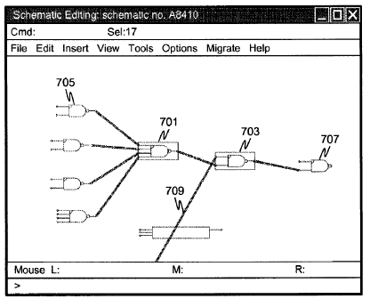
FIG. 7A depicts a schematic for two components of interest before grouping.
The two
components of interest are NAND gate 701 and NAND gate 703. NAND gate 701 has
several
inputs, including 705, as indicated by the flightlines into 705. The NAND gate
703 has two
inputs indicated by the flightline from the output of 701 and the flightline
709 from a component
off the screen. To group the components 701 and 703 the user first selects
them, for example, by
CA 02814339 2013-04-30
WO 2012/063147 PCT/IB2011/054396
drawing a selection box around them or by clicking on each component with the
mouse. The
flightline visualization system allows the user to form a group by enacting
the group command
on the selected components. FIG. 7B shows the results of grouping the two
components 701 and
703.
FIG. 7B depicts the circuit from FIG. 7A with the two components of interest
701 and
703 grouped to be one component 711. The components are replaced by a single
component, but
the connections are preserved. The new group component 711 has all the inputs
of 701 from
FIG. 7A, as well as the input 709 from the component 703. The component 711
has the output to
component 707 also. Note that the flightline between 701 and 703 of FIG. 7A is
not reflected in
FIG. 7B since this flightline is internal to the group making up component
711. In various
embodiments the user is presented with the option of viewing details of the
group, for example,
by hovering over the group component 711.
The component selection feature lets the user selectively group components
into
manageable sets. Thus, a component may be a single atomic circuit element,
such as a transistor
or logic gate. However, a component may also be a group of such elements. The
flightline
visualization system can represent such multi-element components using a
symbol in the main
schematic, and, at the user's request, allow the user to see details of the
group in a schematic all
to itself. This act is commonly known as "descending" through the schematic
hierarchy.
The visualization system can draw flightlines on any schematic, be it the
"top" schematic,
or one of these group schematics. However, it should be noted that the
schematics of the top
level and any specified group are considered to be separate schematics. The
inventors
discovered that a user will often want to see how the internal parts of a
group schematic connect
to the rest of the top schematic. To address this need the visualization
system provides a
function to un-group a component which consists of elements. To do this, the
system first
removes the symbol representing the group from the top schematic. Then, it
places each member
of the group onto the top schematic, taking care to preserve component-to-
component
connectivity. From this point on, the visualization system typically treats
the new components
like any other component.
Just as components can be ungroupcd, so too can components on the top-level
schematic
be regrouped or grouped in different combinations. The visualization system
allows a user to
select one or more components on the top-level schematic, and invoke the
grouping function.
The grouping function creates a new schematic, and gives the group a unique
name (or accepts a
user input for a new group name). The system moves the components selected for
the group
from the top-level schematic to the newly-created schematic. The flightline
visualization system
16
CA 02814339 2013-04-30
WO 2012/063147 PCT/1B2011/054396
may be configured to create pins for the group/component to indicate
connections between a
component moved to the group in the new schematic, and another component
remaining on the
top-level schematic. The system is typically configured to assign these new
pins a suitable
direction, e.g., input, output, supply voltage, or other appropriate category.
The functionality for
grouping components or elements can be associated with a predefined key (e.g.,
the "F6" key) or
other user input such as a drop down menu or the like.
FIGS. 8A and 8B demonstrate the categorization of flightlines as important/
unimportant
and selectively displaying the important flightlines. FIG. 8A depicts a number
of flightlines,
including some flightlincs categorized as unimportant that are then eliminated
from the diagram
depicted in FIG. 8B. It can be helpful in understanding the operation of a
circuit to simplify the
circuit to the extent possible without eliminating signals that contribute to
the functionality or
current state. Various embodiments of the flightline visualization system
include a feature for
reducing the number of flightlines displayed based on current assignments and
computations.
For example, if one input of a 2-input AND gate is set to logic-0, then the
output of the AND
gate must also be logic-0. The second input cannot possibly change the output
value. Therefore
the second input is not important, given that the first input is set to logic-
0, and the flight-line
tool will not normally display it. Furthermore, if the unimportant input is
driven solely by
another gate, then the inputs to the other gate are also not important,
because their value cannot
possible change a known value further along the signal propagation chain.
To determine which flightlines are important, various embodiments can
determine the
"unimportance" of a gate based on the following two decision rules:
= A gate whose output is known, is said to be unimportant.
= A gate that drives ONLY unimportant gates, is also said to be
unimportant.
To determine which flightlines should be rendered, various embodiments can
abide by
the following decision rules:
= A flightline which represents a net having a known value (i.e., either
logic-0 or logic-
1) will always be displayed.
= A flightline will always be displayed if the global setting
"iForceDisplayFlightLines"
is set.
= A flightline which originates at an unimportant gate AND terminates at an
unimportant gate will NOT be displayed.
= If none of the above conditions apply, the default is to display the
flightline.
The user may toggle the "iForceDisplayFlgihtLines" setting by pressing a
predefined key,
e.g., Alt-7.
17
CA 02814339 2013-04-30
WO 2012/063147 PCT/1132011/054396
Turning to FIG. 8A, a number of flightlines are displayed for the NAND gate
801. If
flightline 803 has an assigned value of logic-0 (or is otherwise know to be
logic-0), then the
inputs of flightlines 805, 807 and 809 are don't care function, that is, they
will not affect the
output of component 801 regardless of whether they are logic-0 or logic-1
taken in any
combination. For this reason, the flightlines 805, 807 and 809 are designated
as unimportant
when flightline 803 is known to have a value of logic-0.
FIG. 8B corresponds to FIG. 8A, except with the flightlines 805, 807 and 809
eliminated
since they are categorized as unimportant when flightline 803 is known to be
logic-0. Note that
the NAND gate 801 has a value of logic-1. But this value is not assigned by
the user, rather, it
was computed by the flight-line tool in response to the flightline 803 having
a known value of
logic-0. A NAND gate with one input set to logic-0 will always have an output
of logic-i. In
some embodiments there are other display options for the rest of the input
pins to the NAND
gate 801 rather than showing them with no flightlines attached, as per FIG.
8B. For example, in
some implementations flightlines deemed to be unimportant can be displayed in
a muted manner,
say, by lines that are thinner and less noticeable or in pale colors that are
easy for a user to
disregard.
FIG. 9 depicts a computer system 900 and various components suitable for
implementing
the various embodiments disclosed herein. The computer system 900 may be
configured in the
form of a desktop computer, a laptop computer, a mainframe computer, or any
other hardware or
logic arrangement capable of being programmed or configured to carry out
instructions. In some
embodiments the computer system 900 may act as a server, accepting inputs from
a remote user
over a local area network (LAN) 927, the Internet 929, or an intranet 931. In
other
embodiments, the computer system 900 may function as a smart user interface
device for a
server on the LAN 927 or over the Internet 929. The computer system 900 may be
located and
interconnected in one location, or may be distributed in various locations and
interconnected via
communication links such as a LAN 927 or a wide area network (WAN), via the
Internet 929,
via the public switched telephone network (PSTN), a switching network, a
cellular telephone
network, a wireless link, or other such communication links. Other devices may
also be suitable
for implementing or practicing the embodiments, or a portion of the
embodiments. Such devices
include personal digital assistants (PDA), wireless handsets (e.g., a cellular
telephone or pager),
and other such electronic devices preferably capable of being programmed to
carry out
instructions or routines. Those of ordinary skill in the art may recognize
that many different
architectures may be suitable for the computer system 900, although only one
typical architecture
is depicted in FIG. 9.
18
CA 02814339 2013-04-30
WO 2012/063147 PCT/1132011/054396
Computer system 900 may include a processor 901 which may be embodied as a
microprocessor, two or more parallel processors as shown in FIG. 9, a central
processing unit
(CPU) or other such control logic or circuitry. The processor 901 may be
configured to access a
local cache memory 903, and send requests for data that are not found in the
local cache memory
903 across a cache bus to a second level cache memory 905. Some embodiments
may integrate
the processor 901, and the local cache 903 onto a single integrated circuit
and other embodiments
may utilize a single level cache memory or no cache memory at all. Other
embodiments may
integrate multiple processors 901 onto a single die and/or into a single
package. Yet other
embodiments may integrate multiple processors 901 with multiple local cache
memories 903
with a second level cache memory 905 into a single package 910 with a front
side bus 907 to
communicate to a memory/bus controller 911. The memory/bus controller 911 may
accept
accesses from the processor(s) 901 and direct them to either the internal
memory 913 or to the
various input/output (I/O) busses 909. Some embodiments of the computer system
900 may
include multiple processor packages 910 sharing the front-side bus 907 to the
memory/bus
controller. Other embodiments may have multiple processor packages 910 with
independent
front-side bus connections to the memory/bus controller. The memory bus
controller may
communicate with the internal memory 913 using a memory bus 909.
The internal memory 913 may include one or more of random access memory (RAM)
devices such as synchronous dynamic random access memories (SDRAM), double
data rate
(DDR) memories, or other volatile random access memories. The internal memory
913 may also
include non-volatile memories such as electrically erasable/programmable read-
only memory
(EEPROM), NAND flash memory, NOR flash memory, programmable read-only memory
(PROM), read-only memory (ROM), battery backed-up RAM, or other non-volatile
memories.
In some embodiments, the computer system 900 may also include 3'4 level cache
memory or a
combination of these or other like types of circuitry configured to store
information in a
retrievable format. In some implementations the internal memory 913 may be
configured as part
of the processor 901, or alternatively, may be configured separate from it but
within the same
package 910. The processor 901 may be able to access internal memory 913 via a
different bus
or control lines than is used to access the other components of computer
system 900.
The computer system 900 may also include, or have access to, one or more hard
drives
915 (or other types of storage memory) and optical disk drives 917. Hard
drives 915 and the
optical disks for optical disk drives 917 are examples of machine readable
(also called computer
readable) mediums suitable for storing the final or interim results of the
various embodiments.
The optical disk drives 917 may include a combination of several disc drives
of various formats
19
CA 02814339 2013-04-30
WO 2012/063147 PCT/IB2011/054396
that can read and/or write to removable storage media (e.g., CD-R, CD-RW, DVD,
DVD-R,
DVD-W, DVD-RW, HD-DVD, Blu-Ray, and the like). Other forms or computer
readable media
that may be included in some embodiments of computer system 900 include, but
are not limited
to, floppy disk drives, 9-track tape drives, tape cartridge drives, solid-
state drives, cassette tape
recorders, paper tape readers, bubble memory devices, magnetic strip readers,
punch card readers
or any other type or computer useable or machine readable storage medium.
The computer system 900 may either include the hard drives 915 and optical
disk drives
917 as an integral part of the computer system 900 (e.g., within the same
cabinet or enclosure
and/or using the same power supply), as connected peripherals, or may access
the hard drives
915 and optical disk drives 915 over a network, or a combination of these. The
hard drive 915
often includes a rotating magnetic medium configured for the storage and
retrieval of data,
computer programs or other information. In some embodiments, the hard drive
915 may be a
solid state drive using semiconductor memories. In other embodiments, some
other type of
computer useable medium may be used. The hard drive 915 need not necessarily
be contained
within the computer system 900. For example, in some embodiments the hard
drive 915 may be
server storage space within a network that is accessible to the computer
system 900 for the
storage and retrieval of data, computer programs or other information. In some
instances the
computer system 900 may use storage space at a server storage farm, or like
type of storage
facility, that is accessible by the Internet 929 or other communications
lines. The hard drive 915
is often used to store the software, instructions and programs executed by the
computer system
900, including for example, all or parts of the computer application program
for canying out
activities of the various embodiments.
The communication link 909 may be used to access the contents of the hard
drives 915
and optical disk drives 917. The communication links 909 may be point-to-point
links such as
Serial Advanced Technology Attachment (SATA) or a bus type connection such as
Parallel
Advanced Technology Attachment (PATA) or Small Computer System Interface
(SCSI), a daisy
chained topology such as IEEE-1394, a link supporting various topologies such
as Fibre
Channel, or any other computer communication protocol, standard or
proprietary, that may be
used for communication to computer readable medium. The memory/bus controller
may also
provide other I/O communication links 909. In some embodiments, the links 909
may be a
shared bus architecture such as peripheral component interface (PCI),
microchannel, industry
standard architecture (ISA) bus, extended industry standard architecture
(EISA) bus,
VERSAmodulcEurocard (VME) bus, or any other shared computer bus. In other
embodiments,
the links 909 may be a point-to-point link such as PCI-Express,
HyperTransport, or any other
CA 02814339 2013-04-30
WO 2012/063147 PCT/1132011/054396
point-to-point I/O link. Various I/0 devices may be configured as a part of
the computer system
900.
In many embodiments, a network interface 919 may be included to allow the
computer
system 900 to connect to a network 927 or 931. Either of the networks 927 and
931 may operate
in accordance with standards for an IEEE 802.3 ethernet network, an IEEE
802.11 Wi-Fi
wireless network, or any other type of computer network including, but not
limited to, LANs,
WAN, personal area networks (PAN), wired networks, radio frequency networks,
powerline
networks, and optical networks. A network gateway 933 or router, which may be
a separate
component from the computer system 900 or may be included as an integral part
of the computer
system 900, may be connected to the networks 927 and/or 931 to allow the
computer system 900
to communicate with the Internet 929 over an internet connection such as an
asymmetric digital
subscriber line (ADSL), data over cable service interface specification
(DOCSIS) link, Ti or
other internet connection mechanism. In other embodiments, the computer system
900 may have
a direct connection to the Internet 929. The computer system 900 may be
connected to one or
more other computers such as desktop computer 941 or laptop computer 943 via
the Internet 929,
an intranet 931, and/or a wireless node 945. In some embodiments, an expansion
slot 921 may
be included to allow a user to add additional functionality to the computer
system 900.
The computer system 900 may include an I/O controller 923 providing access to
external
communication interfaces such as universal serial bus (USB) connections,
serial ports such as
RS-232, parallel ports, audio in and audio out connections, the high
performance serial bus
IEEE-1394 and/or other communication links. These connections may also have
separate
circuitry in some embodiments, or may be connected through a bridge to another
computer
communication link provided by the I/O controller 923. A graphics controller
925 may also be
provided to allow applications running on the processor 901 to display
information to a user.
The graphics controller 925 may output video through a video port that may
utilize a standard or
proprietary format such as an analog video graphic array (VGA) connection, a
digital video
interface (DVI), a digital high definition multimedia interface (HDMI)
connection, or any other
video connection. The video connection may connect to display 937 to present
the video
information to the user.
The display 937 may be any of several types of displays or computer monitors,
including
a liquid crystal display (LCD), a cathode ray tube (CRT) monitor, on organic
light emitting diode
(OLED) array, or other type of display suitable for displaying information for
the user. The
display 937 may include one or more light emitting diode (LED) indicator
lights, or other such
display devices. Typically, the computer system 900 includes one or more user
input/output
21
CA 02814339 2013-04-30
WO 2012/063147 PCT/IB2011/054396
(I/O) devices such as a keyboard and mouse 939, and/or other means of
controlling the cursor
represented including but not limited to a touchscreen, touchpad, joystick,
trackball, tablet, or
other device. The user 1/0 devices 935 may connect to the computer system 900
using USB
interfaces or other connections such as RS-232, PS/2 connector or other
interfaces. Various
embodiments include input devices configured to accept an input from a user
and/or provide an
output to a user. For example, some embodiments may include a webcam (e.g.,
connect via
USB), a microphone (e.g., connected to an audio input connection), and/or
speakers (e.g.,
connected to an audio output connection). The computer system 900 typically
has a keyboard
and mouse 939, a monitor 937, and may be configured to include speakers,
microphone, and a
webcam. These input/output devices may be used in various combinations, or
separately, as
means for presenting information to the user and/or receiving information and
other inputs from
a user to be used in carrying out various programs and calculations. Speech
recognition software
may be used in conjunction with the microphone to receive and interpret user
speech commands.
The computer system 900 may be suitable for use in identifying critical web
services and
dynamically relocating them to a new server. For example, the processor 901
may be embodied
as a microprocessor, microcontroller, DSP, RISC processor, two or more
parallel processors, or
any other type of processing unit that one of ordinary skill would recognize
as being capable of
performing or controlling the functions, steps, activities and methods
described herein. A
processing unit in accordance with at least one of the various embodiments can
operate computer
software programs stored (embodied) on non-transitory computer-readable medium
such those
compatible with the disk drives 915, the optical disk drive 917 or any other
type of hard disk
drive, floppy disk, flash memory, ram, or other computer readable medium as
recognized by
those of ordinary skill in the art.
As will be appreciated by those of ordinary skill in the art, aspects of the
various
embodiments may be embodied as a system, method or computer program product.
Accordingly, aspects of the present invention may take the form of an entirely
hardware
embodiment, an entirely software embodiment (including firmware, resident
software, micro-
code, or the like) or an embodiment combining software and hardware aspects
that may all
generally be referred to herein as a "circuit," "module," "logic" or "system."
Furthermore,
aspects of the various embodiments may take the form of a computer program
product embodied
in one or more computer readable medium(s) having computer readable program
code stored
thereon.
Any combination of one or more non-transitory computer readable medium(s) may
be
utilized. The computer readable medium is typically a computer readable
storage medium. A
22
CA 02814339 2013-04-30
WO 2012/063147 PCT/1132011/054396
computer readable storage medium may be embodied as, for example, an
electronic, magnetic,
optical, electromagnetic, infrared, or semiconductor system, apparatus, or
device, or other like
storage devices known to those of ordinary skill in the art, or any suitable
combination of the
foregoing. Examples of such computer readable storage medium include the
following: an
electrical connection having one or more wires, a portable computer diskette,
a hard disk, a
random access memory (RAM), a read-only memory (ROM), an erasable programmable
read-
only memory (EPROM or Flash memory), a portable compact disc read-only memory
(CD-
ROM), an optical storage device, a magnetic storage device, or any suitable
combination of the
foregoing. In the context of this document, a computer readable storage medium
may be any
tangible medium that can contain, or store a program for use by or in
connection with an
instruction execution system, apparatus, or device.
Computer program code for carrying out operations and aspects of the various
embodiments may be written in any combination of one or more programming
languages,
including an object oriented programming language such as Java, Smalltalk,
C++, or the like,
and conventional procedural programming languages, such as the "C" programming
language or
similar programming languages. In accordance with various implementations, the
program code
may execute entirely on the user's computer, partly on the user's computer, as
a stand-alone
software package, partly on the user's computer and partly on a remote
computer or entirely on
the remote computer or server. In the latter scenario, the remote computer may
be connected to
the user's computer through any type of network, including a local area
network (LAN) or a wide
area network (WAN), or the connection may be made to an external computer (for
example,
through the Internet using an Internet Service Provider).
Aspects of the present invention are described with reference to flowchart
illustrations
and/or block diagrams of methods, apparatus, systems, and computer program
products
according to various embodiments disclosed herein. It will be understood that
blocks of the
flowchart illustrations and/or block diagrams, and combinations of blocks in
the flowchart
illustrations and/or block diagrams, can be implemented by computer program
instructions.
These computer program instructions may be provided to a processor of a
general purpose
computer, special purpose computer, or other programmable data processing
apparatus to
produce a machine, such that the instructions, which execute via the processor
of the computer or
other programmable data processing apparatus, create means for implementing
the functions/acts
specified in the flowchart and/or block diagram block or blocks.
These computer program instructions may also be stored in a computer readable
medium
that can direct a computer, a programmable data processing apparatus, or other
such devices to
23
CA 02814339 2013-04-30
WO 2012/063147
PCT/IB2011/054396
function in a particular manner, such that the instructions stored in the
computer readable
medium produce an article of manufacture including instructions which
implement the
function/act specified in the flowchart and/or block diagram block or blocks.
The computer
program instructions may also be loaded onto a computer, other programmable
data processing
apparatus, or other devices to cause a series of operational steps to be
performed on the
computer, other programmable apparatus or other devices to produce a computer
implemented
process such that the instructions which execute on the computer or other
programmable
apparatus provide processes for implementing the functions/acts specified in
the flowchart and/or
block diagram block or blocks.
The flowchart and/or block diagrams in the figures help to illustrate the
architecture,
functionality, and operation of possible implementations of systems, methods
and computer
program products according to various embodiments of the present invention. In
this regard,
each block in the flowchart or block diagrams may represent a module, segment,
or portion of
code, which comprises one or more executable instructions for implementing the
specified
logical function(s),It should also be noted that, in some alternative
implementations, the
functions noted in the block may occur in an order other that that depicted in
the figures. For
example, two blocks shown in succession may, in fact, be executed
substantially concurrently, or
the blocks and activities of the figures may sometimes be executed in reverse
order or in a
different order, depending upon the functionality involved. It will also be
noted that each block
of the block diagrams and/or flowchart illustration, and combinations of
blocks in the block
diagrams and/or flowchart illustration, can be implemented by special purpose
hardware-based
systems that perform the specified functions or acts, or combinations of
special purpose
hardware and computer instructions.
The terminology used herein is for the purpose of describing particular
embodiments only
and is not intended to be limiting of the invention. As used herein, the
singular forms "a", "an"
and "the" are intended to include the plural forms as well, unless the context
clearly indicates
otherwise. It will be further understood that the terms "comprises,"
"comprising," "includes,"
and/or "including" used in this specification specify the presence of stated
features, integers,
steps, operations, elements, and/or components, but do not preclude the
presence or addition of
one or more other features, integers, steps, operations, elements, components,
and/or groups
thereof. The term "obtaining", as used herein and in the claims, may mean
either retrieving from
a computer readable storage medium, receiving from another computer program,
receiving from
a user, calculating based on other input, or any other means of obtaining a
datum or set of data.
The term "plurality", as used herein and in the claims, means two or more of a
named element.
24
CA 02814339 2013-04-30
WO 2012/063147 PCT/IB2011/054396
It should not, however, be interpreted to necessarily refer to every instance
of the named element
in the entire device. Particularly, if there is a reference to "each" element
of a "plurality" of
elements. There may be additional elements in the entire device that are not
be included in the
"plurality" and are not, therefore, referred to by "each."
The corresponding structures, materials, acts, and equivalents of all means or
step plus
function elements in the claims below are intended to include any structure,
material, or act for
performing the function in combination with other claimed elements as
specifically claimed.
The description of the present invention has been presented for purposes of
illustration and
description, but is not intended to be exhaustive or limited to the invention
in the form disclosed.
Many modifications and variations will be apparent to those of ordinary skill
in the art without
departing from the scope and gist of the invention. The various embodiments
included herein
were chosen and described in order to best explain the principles of the
invention and the
practical application, and to enable others of ordinary skill in the art to
understand the invention
for various embodiments with various modifications as are suited to the
particular use
contemplated.