Note: Descriptions are shown in the official language in which they were submitted.
CA 2814635 2017-05-26
=
SURFACE SCATTERING ANTENNAS
WITH ADJUSTABLE RADIATION FIELDS
BACKGROUND
The application discloses an antenna and method of use for the antenna to
provide
adjustable radiation fields by adjusting coupling scattering elements along a
wave-
propagating structure.
US 7,253,780 B2 discloses a steerable leaky wave antenna capable of both
forward and
backward radiation.
US 2002/167456 Al discloses a reconfigurable artificial magnetic conductor
using
voltage controlled capacitors with a coplanar resistive biasing network.
WO 2010/021736 A2 discloses complementary metamaterial elements which
provide an effective permittivity and/or permeability for surface structures
and/or
waveguide structures.
US 6,232,931 B1 discloses an optically controlled frequency selective surface
which includes an electrically conductive layer having an array of radio
frequency
scattering elements such as slots formed in an electrically conductive layer
or loops
mounted to a substrate.
US 6,552,696 B1 discloses a tunable impedance surface for steering and/or
focusing a radio frequency beam.
- 1 -
CA 02814635 2016-11-22
10
BRIEF DESCRIPTION OF THE FIGURES
FIG. 1 is a schematic depiction of a surface scattering antenna.
FIGS. 2A and 2B respectively depict an exemplary adjustment pattern and
corresponding beam pattern for a surface scattering antenna.
FIGS. 3A and 3B respectively depict another exemplary adjustment pattern
and corresponding beam pattern for a surface scattering antenna.
FIGS. 4A and 4B respectively depict another exemplary adjustment pattern
and corresponding field pattern for a surface scattering antenna.
FIGS. 5 and 6 depict a unit cell of a surface scattering antenna.
FIG. 7 depicts examples of metamaterial elements.
FIG. 8 depicts a microstrip embodiment of a surface scattering antenna.
FIG. 9 depicts a coplanar waveguide embodiment of a surface scattering
antenna.
FIGS. 10 and 11 depict a closed waveguide embodiments of a surface
scattering antenna.
FIG. 12 depicts a surface scattering antenna with direct addressing of the
scattering elements.
FIG. 13 depicts a surface scattering antenna with matrix addressing of the
scattering elements.
FIG. 14 depicts a system block diagram.
- 2 -
CA 02814635 2016-11-22
FIGS. 15 and 16 depict flow diagrams.
DETAILED DESCRIPTION
In the following detailed description, reference is made to the accompanying
drawings, which form a part hereof. In the drawings, similar symbols typically
__ identify similar components, unless context dictates otherwise. The
illustrative
embodiments described in the detailed description, drawings, and claims are
not
meant to be limiting. Other embodiments may be utilized, and other changes may
be
made, without departing from the spirit or scope of the subject matter
presented here.
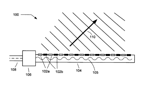
A schematic illustration of a surface scattering antenna is depicted in FIG.
1.
The surface scattering antenna 100 includes a plurality of scattering elements
102a,
102b that are distributed along a wave-propagating structure 104. The wave
propagating structure 104 may be a microstrip, a coplanar waveguide, a
parallel plate
waveguide, a dielectric slab, a closed or tubular waveguide, or any other
structure
capable of supporting the propagation of a guided wave or surface wave 105
along or
within the structure. The wavy line 105 is a symbolic depiction of the guided
wave or
surface wave, and this symbolic depiction is not intended to indicate an
actual
wavelength or amplitude of the guided wave or surface wave; moreover, while
the
wavy line 105 is depicted as within the wave-propagating structure 104 (e.g.
as for a
guided wave in a metallic waveguide), for a surface wave the wave may be
substantially localized outside the wave-propagating structure (e.g. as for a
TM mode
on a single wire transmission line or a "spoof plasmon" on an artificial
impedance
surface). The scattering elements 102a, 102b may include metamaterial elements
that
are embedded within, positioned on a surface of, or positioned within an
evanescent
proximity of, the wave-propagation structure 104; for example, the scattering
elements can include complementary metamaterial elements such as those
presented
in D. R. Smith et al, "Metamaterials for surfaces and waveguides," U.S. Patent
Application Publication No. 2010/0156573.
The surface scattering antenna also includes at least one feed connector 106
that is configured to couple the wave-propagation structure 104 to a feed
structure
- 3 -
CA 028146352013-04-12
WO 2012/050614
PCT/US2011/001755
108. The feed structure 108 (schematically depicted as a coaxial cable) may be
a
transmission line, a waveguide, or any other structure capable of providing an
electromagnetic signal that may be launched, via the feed connector 106, into
a
guided wave or surface wave 105 of the wave-propagating structure 104. The
feed
connector 106 may be, for example, a coaxial-to-microstrip connector (e.g. an
SMA-
to-PCB adapter), a coaxial-to-waveguide connector, a mode-matched transition
section, etc.. While FIG. 1 depicts the feed connector in an "end-launch"
configuration, whereby the guided wave or surface wave 105 may be launched
from a
peripheral region of the wave-propagating structure (e.g. from an end of a
microstrip
or from an edge of a parallel plate waveguide), in other embodiments the feed
structure may be attached to a non-peripheral portion of the wave-propagating
structure, whereby the guided wave or surface wave 105 may be launched from
that
non-peripheral portion of the wave-propagating structure (e.g. from a midpoint
of a
microstrip or through a hole drilled in a top or bottom plate of a parallel
plate
waveguide); and yet other embodiments may provide a plurality of feed
connectors
attached to the wave-propagating structure at a plurality of locations
(peripheral
and/or non-peripheral).
The scattering elements 102a, 102b are adjustable scattering elements having
electromagnetic properties that are adjustable in response to one or more
external
inputs. Various embodiments of adjustable scattering elements are described,
for
example, in D. R. Smith et al, previously cited, and further in this
disclosure.
Adjustable scattering elements can include elements that are adjustable in
response to
voltage inputs (e.g. bias voltages for active elements (such as varactors,
transistors,
diodes) or for elements that incorporate tunable dielectric materials (such as
ferroelectrics)), current inputs (e.g. direct injection of charge carriers
into active
elements), optical inputs (e.g. illumination of a photoactive material), field
inputs
(e.g. magnetic fields for elements that include nonlinear magnetic materials),
mechanical inputs (e.g. MEMS, actuators, hydraulics), etc. In the schematic
example
of FIG. 1, scattering elements that have been adjusted to a first state having
first
electromagnetic properties are depicted as the first elements 102a, while
scattering
elements that have been adjusted to a second state having second
electromagnetic
- 4 -
00 02814635 2013-01-12
WO 2012/050614
PCT/US2011/001755
properties are depicted as the second elements 102b. The depiction of
scattering
elements having first and second states corresponding to first and second
electromagnetic properties is not intended to be limiting: embodiments may
provide
scattering elements that are discretely adjustable to select from a discrete
plurality of
states corresponding to a discrete plurality of different electromagnetic
properties, or
continuously adjustable to select from a continuum of states corresponding to
a
continuum of different electromagnetic properties. Moreover, the particular
pattern
of adjustment that is depicted in FIG. 1 (i.e. the alternating arrangement of
elements
102a and 102b) is only an exemplary configuration and is not intended to be
limiting.
In the example of FIG. 1, the scattering elements 102a, 102b have first and
second couplings to the guided wave or surface wave 105 that are functions of
the
first and second electromagnetic properties, respectively. For example, the
first and
second couplings may be first and second polarizabilities of the scattering
elements at
the frequency or frequency band of the guided wave or surface wave. In one
approach the first coupling is a substantially nonzero coupling whereas the
second
coupling is a substantially zero coupling. In another approach both couplings
are
substantially nonzero but the first coupling is substantially greater than (or
less than)
than the second coupling. On account of the first and second couplings, the
first and
second scattering elements 102a, 102b are responsive to the guided wave or
surface
.. wave 105 to produce a plurality of scattered electromagnetic waves having
amplitudes that are functions of (e.g. are proportional to) the respective
first and
second couplings. A superposition of the scattered electromagnetic waves
comprises
an electromagnetic wave that is depicted, in this example, as a plane wave 110
that
radiates from the surface scattering antenna 100.
The emergence of the plane wave may be understood by regarding the
particular pattern of adjustment of the scattering elements (e.g. an
alternating
arrangement of the first and second scattering elements in FIG. 1) as a
pattern that
defines a grating that scatters the guided wave or surface wave 105 to produce
the
plane wave 110. Because this pattern is adjustable, some embodiments of the
surface
scattering antenna may provide adjustable gratings or, more generally,
holograms,
where the pattern of adjustment of the scattering elements may be selected
according
- 5 -
CA 028146352013-04-12
WO 2012/050614
PCT/US2011/001755
to principles of holography. Suppose, for example, that the guided wave or
surface
wave may be represented by a complex scalar input wave Tin that is a function
of
position along the wave-propagating structure 104, and it is desired that the
surface
scattering antenna produce an output wave that may be represented by another
.. complex scalar wave 'P., . Then a pattern of adjustment of the scattering
elements
may be selected that corresponds to a an interference pattern of the input and
output
waves along the wave-propagating structure. For example, the scattering
elements
may be adjusted to provide couplings to the guided wave or surface wave that
are
functions of (e.g. are proportional to, or step-functions of) an interference
term given
by Re['-outtlii*õ]. In this way, embodiments of the surface scattering antenna
may be
adjusted to provide arbitrary antenna radiation patterns by identifying an
output wave
P.u, corresponding to a selected beam pattern, and then adjusting the
scattering
elements accordingly as above. Embodiments of the surface scattering antenna
may
therefore be adjusted to provide, for example, a selected beam direction (e.g.
beam
steering), a selected beam width or shape (e.g. a fan or pencil beam having a
broad or
narrow beamwidth), a selected arrangement of nulls (e.g. null steering), a
selected
arrangement of multiple beams, a selected polarization state (e.g. linear,
circular, or
elliptical polarization), a selected overall phase, or any combination
thereof.
Alternatively or additionally, embodiments of the surface scattering antenna
may be
adjusted to provide a selected near field radiation profile, e.g. to provide
near-field
focusing and/or near-field nulls.
Because the spatial resolution of the interference pattern is limited by the
spatial resolution of the scattering elements, the scattering elements may be
arranged
along the wave-propagating structure with inter-element spacings that are much
less
than a free-space wavelength corresponding to an operating frequency of the
device
(for example, less than one-fourth of one-fifth of this free-space
wavelength). In
some approaches, the operating frequency is a microwave frequency, selected
from
frequency bands such as Ka, Ku, and Q, corresponding to centimeter-scale free-
space
wavelengths. This length scale admits the fabrication of scattering elements
using
conventional printed circuit board technologies, as described below.
- 6 -
CA 028146352013-04-12
WO 2012/050614
PCT/US2011/001755
In some approaches, the surface scattering antenna includes a substantially
one-dimensional wave-propagating structure 104 having a substantially one-
dimensional arrangement of scattering elements, and the pattern of adjustment
of this
one-dimensional arrangement may provide, for example, a selected antenna
radiation
profile as a function of zenith angle (i.e. relative to a zenith direction
that is parallel to
the one-dimensional wave-propagating structure). In other approaches, the
surface
scattering antenna includes a substantially two-dimensional wave-propagating
structure 104 having a substantially two-dimensional arrangement of scattering
elements, and the pattern of adjustment of this two-dimensional arrangement
may
provide, for example, a selected antenna radiation profile as a function of
both zenith
and azimuth angles (i.e. relative to a zenith direction that is perpendicular
to the two-
dimensional wave-propagating structure). Exemplary adjustment patterns and
beam
patterns for a surface scattering antenna that includes a two-dimensional
array of
scattering elements distributed on a planar rectangular wave-propagating
structure are
depicted in FIGS. 2A ¨ 4B. In these exemplary embodiments, the planar
rectangular
wave-propagating structure includes a monopole antenna feed that is positioned
at the
geometric center of the structure. FIG. 2A presents an adjustment pattern that
corresponds to a narrow beam having a selected zenith and azimuth as depicted
by the
beam pattern diagram of FIG. 2B. FIG. 3A presents an adjustment pattern that
corresponds to a dual-beam far field pattern as depicted by the beam pattern
diagram
of FIG. 3B. FIG. 4A presents an adjustment pattern that provides near-field
focusing
as depicted by the field intensity map of FIG. 4B (which depicts the field
intensity
along a plane perpendicular to and bisecting the long dimension of the
rectangular
wave-propagating structure).
In some approaches, the wave-propagating structure is a modular wave-
propagating structure and a plurality of modular wave-propagating structures
may be
assembled to compose a modular surface scattering antenna. For example, a
plurality
of substantially one-dimensional wave-propagating structures may be arranged,
for
example, in an interdigital fashion to produce an effective two-dimensional
arrangement of scattering elements. The interdigital arrangement may comprise,
for
example, a series of adjacent linear structures (i.e. a set of parallel
straight lines) or a
- 7 -
00 02814635 2013 04-12
WO 2012/050614
PCT/US2011/001755
series of adjacent curved structures (i.e. a set of successively offset curves
such as
sinusoids) that substantially fills a two-dimensional surface area. As another
example, a plurality of substantially two-dimensional wave-propagating
structures
(each of which may itself comprise a series of one-dimensional structures, as
above)
may be assembled to produce a larger aperture having a larger number of
scattering
elements; and/or the plurality of substantially two-dimensional wave-
propagating
structures may be assembled as a three-dimensional structure (e.g. forming an
A-
frame structure, a pyramidal structure, or other multi-faceted structure). In
these
modular assemblies, each of the plurality of modular wave-propagating
structures
may have its own feed connector(s) 106, and/or the modular wave-propagating
structures may be configured to couple a guided wave or surface wave of a
first
modular wave-propagating structure into a guided wave or surface wave of a
second
modular wave-propagating structure by virtue of a connection between the two
structures.
In some applications of the modular approach, the number of modules to be
assembled may be selected to achieve an aperture size providing a desired
telecommunications data capacity and/or quality of service, and/or a three-
dimensional arrangement of the modules may be selected to reduce potential
scan
loss. Thus, for example, the modular assembly could comprise several modules
.. mounted at various locations/orientations flush to the surface of a vehicle
such as an
aircraft, spacecraft, watercraft, ground vehicle, etc. (the modules need not
be
contiguous). In these and other approaches, the wave-propagating structure may
have
a substantially non-linear or substantially non-planar shape whereby to
conform to a
particular geometry, therefore providing a conformal surface scattering
antenna
(conforming, for example, to the curved surface of a vehicle).
More generally, a surface scattering antenna is a reconfigurable antenna that
may be reconfigured by selecting a pattern of adjustment of the scattering
elements so
that a corresponding scattering of the guided wave or surface wave produces a
desired
output wave. Suppose, for example, that the surface scattering antenna
includes a
plurality of scattering elements distributed at positions {19 along a wave-
propagating
structure 104 as in FIG. 1 (or along multiple wave-propagating structures, for
a
- 8 -
00 02814635 2013 04-12
WO 2012/050614
PCT/US2011/001755
modular embodiment) and having a respective plurality of adjustable couplings
(a}
to the guided wave or surface wave 105. The guided wave or surface wave 105,
as it
propagates along or within the (one or more) wave-propagating structure(s),
presents
a wave amplitude and phase v., to the jth scattering element; subsequently,
an
output wave is generated as a superposition of waves scattered from the
plurality of
scattering elements:
EOM = ER, (04)011,V, ej(k( 95)5j) (1)
where E(9, ) represents the electric field component of the output wave on a
far-
field radiation sphere, 111 (0, 0) represents a (normalized) electric field
pattern for the
scattered wave that is generated by the jth scattering element in response to
an
excitation caused by the coupling a3, and k(8, 0) represents a wave vector of
magnitude co I c that is perpendicular to the radiation sphere at (9 50) .
Thus,
embodiments of the surface scattering antenna may provide a reconfigurable
antenna
that is adjustable to produce a desired output wave E(0,0) by adjusting the
plurality
of couplings {a3} in accordance with equation (1).
The wave amplitude Ai and phase yoi of the guided wave or surface wave are
functions of the propagation characteristics of the wave-propagating structure
104.
These propagation characteristics may include, for example, an effective
refractive
index and/or an effective wave impedance, and these effective electromagnetic
properties may be at least partially determined by the arrangement and
adjustment of
the scattering elements along the wave-propagating structure. In other words,
the
wave-propagating structure, in combination with the adjustable scattering
elements,
may provide an adjustable effective medium for propagation of the guided wave
or
surface wave, e.g. as described in D. R. Smith et al, previously cited.
Therefore,
although the wave amplitude Ai and phase col of the guided wave or surface
wave
may depend upon the adjustable scattering element couplings {a3} (i.e.
= A,({c t i}) 5 cc1 = 9,({a})), in some embodiments these dependencies may be
- 9 -
00 02814635 2013-01-12
WO 2012/050614
PCT/US2011/001755
substantially predicted according to an effective medium description of the
wave-
propagating structure.
In some approaches, the reconfigurable antenna is adjustable to provide a
desired polarization state of the output wave E(0,0). Suppose, for example,
that first
and second subsets LP(') and LP(2) of the scattering elements provide
(normalized)
electric field patterns R(I)(0,0) and W2)(8,0), respectively, that are
substantially
linearly polarized and substantially orthogonal (for example, the first and
second
subjects may be scattering elements that are perpendicularly oriented on a
surface of
the wave-propagating structure 104). Then the antenna output wave E(0,0) may
be
expressed as a sum of two linearly polarized components:
E(0, 0) = E(') (0, 0) + V') (8,0) = A(DR(1)(0, 0) + A(2)R(2) (0, 0), (2)
where
A '2(0, ) =_. (3)
I I
jeLp(1.2)
E a A ei9 ei(k(9,0)Lid
are the complex amplitudes of the two linearly polarized components.
Accordingly,
the polarization of the output wave E(0,0) may be controlled by adjusting the
plurality of couplings {oti} in accordance with equations (2)-(3), e.g. to
provide an
output wave with any desired polarization (e.g. linear, circular, or
elliptical).
Alternatively or additionally, for embodiments in which the wave-propagating
structure has a plurality of feeds (e.g. one feed for each "finger" of an
interdigital
arrangement of one-dimensional wave-propagating structures, as discussed
above), a
desired output wave E(0,0) may be controlled by adjusting gains of individual
amplifiers for the plurality of feeds. Adjusting a gain for a particular feed
line would
correspond to multiplying the Ai's by a gain factor G for those elements j
that are
fed by the particular feed line. Especially, for approaches in which a first
wave-
propagating structure having a first feed (or a first set of such
structures/feeds) is
coupled to elements that are selected from _Lk') and a second wave-propagating
structure having a second feed (or a second set of such structures/feeds) is
coupled to
elements that are selected from LP(2), depolarization loss (e.g., as a beam is
scanned
-10-
CA 02814635 2016-11-22
off-broadside) may be compensated by adjusting the relative gain(s) between
the first
feed(s) and the second feed(s).
As mentioned previously in the context of FIG. 1, in some approaches the
surface scattering antenna 100 includes a wave-propagating structure 104 that
may be
implemented as a microstrip or a parallel plate waveguide (or a plurality of
such
elements); and in these approaches, the scattering elements may include
complementary metamaterial elements such as those presented in D.R. Smith et
at,
previously cited. Turning now to FIG. 5, an exemplary unit cell 500 of a
microstrip
or parallel-plate waveguide is depicted that includes a lower conductor or
ground
plane 502 (made of copper or similar material), a dielectric substrate 504
(made of
Duriod, FR4, or similar material), and an upper conductor 506 (made of copper
or
similar material) that embeds a complementary metamaterial element 510, in
this case
a complementary electric LC (CELC) metamaterial element that is defined by a
shaped aperture 512 that has been etched or patterned in the upper conductor
(e.g. by
a PCB process).
A CELC element such as that depicted in FIG. 5 is substantially responsive to
a magnetic field that is applied parallel to the plane of the CELC element and
perpendicular to the CELC gap complement, i.e. in the direction for the for
the
orientation of FIG. 5 (cf. T. H. Hand et al, "Characterization of
complementary
electric field coupled resonant surfaces," Applied Physics Letters 93,
212504(2008).
Therefore, a magnetic field component of a guided
wave that propagates in the microstrip or parallel plate waveguide (being an
instantiation of the guided wave or surface wave 105 of FIG. 1) can induce a
magnetic excitation of the element 510 that may be substantially characterized
as a
magnetic dipole excitation oriented in direction, thus producing a
scattered
electromagnetic wave that is substantially a magnetic dipole radiation field.
Noting that the shaped aperture 512 also defines a conductor island 514 which
is electrically disconnected from the upper conductor 506, in some approaches
the
scattering element can be made adjustable by providing an adjustable material
within
and/or proximate to the shaped aperture 512 and subsequently applying a bias
voltage
between the conductor island 514 and the upper conductor 506. For example, as
- 11 -
CA 02814635 2016-11-22
shown in FIG. 5, the unit cell may be immersed in a layer of liquid crystal
material
520. Liquid crystals have a permittivity that is a function of orientation of
the
molecules comprising the liquid crystal; and that orientation may be
controlled by
applying a bias voltage (equivalently, a bias electric field) across the
liquid crystal;
accordingly, liquid crystals can provide a voltage-tunable permittivity for
adjustment
of the electromagnetic properties of the scattering element.
The liquid crystal material 520 may be retained in proximity to the scattering
elements by, for example, providing a liquid crystal containment structure on
the
upper surface of the wave-propagating structure, An exemplary configuration of
a
.. liquid crystal containment structure is shown in FIG. 5, which depicts a
liquid crystal
containment structure that includes a covering portion 532 and, optionally,
one or
more support portions or spacers 534 that provide a separation between the
upper
conductor 506 and the covering portion 532. In some approaches, the liquid
crystal
containment structure is a machined or injection-molded plastic part having a
flat
surface that may be joined to the upper surface of the wave-propagating
structure, the
flat surface including one or more indentations (e.g. grooves or recesses)
that may be
overlaid on the scattering elements; and these indentations may be filled with
liquid
crystal by, for example, a vacuum injection process. In other approaches, the
support
portions 534 are spherical spacers (e.g. spherical resin particles); or walls
or pillars
that are formed by a photolithographic process (e.g. as described in Sato et
al,
"Method for manufacturing liquid crystal device with spacers formed by
photolithography," U.S. Patent No. 4,874,46l; the
covering portion 532 is then affixed to the support portions 534, followed by
installation (e.g. by vacuum injection) of the liquid crystal.
For a nematic phase liquid crystal, wherein the molecular orientation may be
characterized by a director field, the material may provide a larger
permittivity LI, for
an electric field component that is parallel to the director and a smaller
permittivity
ei for an electric field component that is perpendicular to the director.
Applying a
bias voltage introduces bias electric field lines that span the shaped
aperture and the
director tends to align parallel to these electric field lines (with the
degree of
alignment increasing with bias voltage). Because these bias electric field
lines are
- 12 -
CA 028146352013-04-12
WO 2012/050614
PCT/US2011/001755
substantially parallel to the electric field lines that are produced during a
scattering
excitation of the scattering element, the permittivity that is seen by the
biased
scattering element correspondingly tends towards en (i.e. with increasing bias
voltage). On the other hand, the permittivity that is seen by the unbiased
scattering
element may depend on the unbiased configuration of the liquid crystal. When
the
unbiased liquid crystal is maximally disordered (i.e. with randomly oriented
micro-
domains), the unbiased scattering element may see an averaged permittivity
(e0 + el) / 2. When the unbiased liquid crystal is maximally aligned
perpendicular to the bias electric field lines (i.e. prior to the application
of the bias
electric field), the unbiased scattering element may see a permittivity as
small as el.
Accordingly, for embodiments where it is desired to achieve a greater range of
tuning
of the permittivity that is seen by the scattering element (corresponding to a
greater
range of tuning of an effective capacitance of the scattering element and
therefore a
greater range of tuning of a resonant frequency of the scattering element),
the unit cell
500 may include positionally-dependent alignment layer(s) disposed at the top
and/or
bottom surface of the liquid crystal layer 510, the positionally-dependent
alignment
layer(s) being configured to align the liquid crystal director in a direction
substantially perpendicular to the bias electric field lines that correspond
an applied
bias voltage. The alignment layer(s) may include, for example, polyimide
layer(s)
that are rubbed or otherwise patterned (e.g. by machining or photolithography)
to
introduce microscopic grooves that run parallel to the channels of the shaped
aperture
512.
Alternatively or additionally, the unit cell may provide a first biasing that
aligns the liquid crystal substantially perpendicular to the channels of the
shaped
aperture 512 (e.g. by introducing a bias voltage between the upper conductor
506 and
the conductor island 514, as described above), and a second biasing that
aligns the
liquid crystal substantially parallel to the channels of the shaped aperture
512 (e.g. by
introducing electrodes positioned above the upper conductor 506 at the four
corners
of the units cell, and applying opposite voltages to the electrodes at
adjacent corners);
tuning of the scattering element may then be accomplished by, for example,
- 13 -
CA 02814635 2016-11-22
alternating between the first biasing and the second biasing, or adjusting the
relative
strengths of the first and second biasings.
In some approaches, a sacrificial layer may be used to enhance the effect of
the liquid crystal tuning by admitting a greater volume of liquid crystal
within a
.. vicinity of the shaped aperture 512. An illustration of this approach is
depicted in
FIG. 6, which shows the unit cell 500 of FIG. 5 in profile, with the addition
of a
sacrificial layer 600 (e.g. a polyimide layer) that is deposited between the
dielectric
substrate 504 and the upper conductor 506. Subsequent to etching of the upper
conductor 506 to define the shaped aperture 512, a further selective etching
of the
sacrificial layer 600 produces cavities 602 that may then be filled with the
liquid
crystal 520. In some approaches another masking layer is used (instead of or
in
addition to making by the upper conductor 506) to define the pattern of
selective
etching of the sacrificial layer 600.
Exemplary liquid crystals that may be deployed in various embodiments
include 4-Cyano-4'-pentylbiphenyl, high birefringence eutectic LC mixtures
such as
LCMS-107 (LC Matter) or GT3-23001 (Merck). Some approaches may utilize dual-
frequency liquid crystals. In dual-frequency liquid crystals, the director
aligns
substantially parallel to an applied bias field at a lower frequencies, but
substantially
perpendicular to an applied bias field at higher frequencies. Accordingly, for
.. approaches that deploy these dual-frequency liquid crystals, tuning of the
scattering
elements may be accomplished by adjusting the frequency of the applied bias
voltage
signals. Other approaches may deploy polymer network liquid crystals (PNLCs)
or
polymer dispersed liquid crystals (PDLCs), which generally provide much
shorter
relaxation/switching times for the liquid crystal. An example of the former is
a
thermal or UV cured mixture of a polymer (such as BPA-dimethacrylate) in a
nematic
LC host (such as LCMS-107); cf. Y.H. Fan et al, "Fast-response and scattering-
free
polymer network liquid crystals for infrared light modulators," Applied
Physics
Letters 84, 1233-35 (2004). An example of the
latter is a porous polymer material (such as a PTFE membrane) impregnated with
a
nematic LC (such as LCMS-107); cf. T. Kuki et al, "Microwave variable delay
line
using a membrane impregnated with liquid crystal," Microwave Symposium Digest,
- 14 -
CA 02814635 2016-11-22
2002 IEEE MTT-S International, vol.1, pp.363-366 (2002).
Turning now to approaches for providing a bias voltage between the
conductor island 514 and the upper conductor 506, it is first noted that the
upper
conductor 506 extends contiguously from one unit cell to the next, so an
electrical
connection to the upper conductor of every unit cell may be made by a single
connection to the upper conductor of the microstrip or parallel-plate
waveguide of
which unit cell 500 is a constituent. As for the conductor island 514, FIG. 5
shows
an example of how a bias voltage line 530 may be attached to the conductor
island.
In this example, the bias voltage line 530 is attached at the center of the
conductor
island and extends away from the conductor island along an plane of symmetry
of the
scattering element; by virtue of this positioning along a plane of symmetry,
electric
fields that are experienced by the bias voltage line during a scattering
excitation of the
scattering element are substantially perpendicular to the bias voltage line
and
therefore do not excite currents in the bias voltage line that could disrupt
or alter the
scattering properties of the scattering element. The bias voltage line 530 may
be
installed in the unit cell by, for example, depositing an insulating layer
(e.g.
polyimide), etching the insulating layer at the center of the conductor island
514, and
then using a lift-off process to pattern a conducting film (e.g. a Cr/Au
bilayer) that
defines the bias voltage line 530.
FIGS. 7A-711 depict a variety of CELC elements that may be used in
accordance with various embodiments of a surface scattering antenna. These are
schematic depictions of exemplary elements, not drawn to scale, and intended
to be
merely representative of a broad variety of possible CELC elements suitable
for
various embodiments. FIG. 7A corresponds to the element used in FIG. 5. FIG.
7B
depicts an alternative CELC element that is topologically equivalent to that
of 7A, but
which uses an undulating perimeter to increase the lengths of the arms of the
element,
thereby increasing the capacitance of the element. FIGS. 7C and 7D depict a
pair of
element types that may be utilized to provide polarization control. When these
orthogonal elements are excited by a guided wave or surface wave having a
magnetic
field oriented in the 57 direction, this applied magnetic field produces
magnetic
- 15-
CA 09814635 901S-04-12
WO 2012/050614
PCT/US2011/001755
excitations that may be substantially characterized as magnetic dipole
excitations,
oriented at +45 or -45 relative to the direction for the element of 7C or
7D,
respectively. FIGS. 7E and 7F depict variants of such orthogonal CELC elements
in
the which the arms of the CELC element are also slanted at a 45 angle. These
slanted designs potentially provide a purer magnetic dipole response, because
all of
the regions of the CELC element that give rise to the dipolar response are
either
oriented orthogonal to the exciting field (and therefore not excited) or at a
45 angle
with respect to that field. Finally, FIGS. 7E and 7F depict similarly slanted
variants
of the undulated CELC element of FIG. 7B.
While FIG. 5 presents an example of a metamaterial element 510 that is
patterned on the upper conductor 506 of a wave-propagating structure such as a
microstrip, in another approach, as depicted in FIG. 8, the metamaterial
elements are
not positioned on the microstrip itself; rather, they are positioned within an
evanescent proximity of (i.e. within the fringing fields of) a microstrip.
Thus, FIG. 8
depicts a microstrip configuration having a ground plane 802, a dielectric
substrate
804, and an upper conductor 806, with conducting strips 808 positioned along
either
side of the microstrip. These conducting strips 808 embed complementary
metamaterial elements 810 defined by shaped apertures 812. In this example,
the
complementary metamaterial elements are undulating-perimeter CELC elements
such
as that shown in FIG. 7B. As shown in FIG. 8, a via 840 can be used to connect
a
bias voltage line 830 to the conducting island 814 of each metamaterial
element. As a
result, this configuration can be readily implemented using a two-layer PCB
process
(two conducting layers with an intervening dielectric), with layer 1 providing
the
microstrip signal trace and metamaterial elements, and layer 2 providing the
microstrip ground plane and biasing traces. The dielectric and conducting
layers may
be high efficiency materials such as copper-clad Rogers 5880. As before,
tuning may
be accomplished by disposing a layer of liquid crystal (not shown) above the
metamaterial elements 810.
In yet another approach, as depicted in FIGS. 9A and 9B, the wave-
propagating structure is a coplanar waveguide (CPW), and the metamaterial
elements
are positioned within an evanescent proximity of (i.e. within the fringing
fields of) the
- 16-
CA 02811635 2013 01 12
WO 2012/050614
PCT/US2011/001755
coplanar waveguide. Thus, FIGS. 9A and 9B depict a coplanar waveguide
configuration having a lower ground plane 902, central ground planes 906 on
either
side of a CPW signal trace 907, and an upper ground plane 910 that embeds
complementary metamaterial elements 920 (only one is shown, but the approach
positions a series of such elements along the length of the CPW). These
successive
conducting layers are separated by dielectric layers 904, 908. The coplanar
waveguide may be bounded by colonnades of vias 930 that can serve to cut off
higher
order modes of the CPW and/or reduce crosstalk with adjacent CPWs (not shown).
The CPW strip width 909 can be varied along the length of the CPW to control
the
couplings to the metamaterial elements 920, e.g. to enhance aperture
efficiency and/or
control aperture tapering of the beam profile. The CPW gap width 911 can be
adjusted the control the line impedance. As shown in FIG. 9B, a third
dielectric layer
912 and a through-via 940 can be used to connect a bias voltage line 950 to
the
conducting island 922 of each metamaterial element and to a biasing pad 952
situated
on the underside of the structure. Channels 924 in the third dielectric layer
912 admit
the disposal of the liquid crystal (not shown) within the vicinities of the
shaped
apertures of the conducting element. This configuration can be implemented
using a
four-layer PCB process (four conducting layers with three intervening
dielectric
layers). These PCBs may be manufactured using lamination stages along with
through, blind and buried via formation as well as electroplating and
electroless
plating techniques.
In still another approach, depicted in FIGS. 10 and 11, the wave-propagating
structure is a closed, or tubular, waveguide, and the metamaterial elements
are
positioned along the surface of the closed waveguide. Thus, FIG. 10 depicts a
closed, or tubular, waveguide with a rectangular cross section defined by a
trough
1002 and a conducting surface 1004 that embeds the metamaterial element 1010.
As
the cutaway shows, a via 1020 through a dielectric layer 1022 can be used to
connect
a bias voltage line 1030 to the conducting island 1012 of the metamaterial
element.
The trough 1002 can be implemented as a piece of metal that is milled or cast
to
provide the "floor and walls" of the closed waveguide, and the waveguide
"ceiling"
can be implemented as a two-layer printed circuit board, with the top layer
providing
-17-
CA 02811635 2013 01 12
WO 2012/050614
PCT/US2011/001755
the biasing traces 1030 and the bottom layer providing the metamaterial
elements
1010. The waveguide may be loaded with a dielectric 1040 (such as PTFE) having
a
smaller trough 1050 that can be filled with liquid crystal to admit tuning of
the
metamaterial elements.
In an alternative closed waveguide embodiment as depicted in FIG. 11, a
closed waveguide with a rectangular cross section is defined by a trough 1102
and
conducting surface 1104. As the unit cell cutaway shows, the conductor surface
1104
has an iris 1106 that admits coupling between a guided wave and the resonator
element 1110. In this example, the complementary metamaterial element is an
undulating-perimeter CELC element such as that shown in FIG. 7B. While the
figure
depicts a rectangular coupling iris, other shapes can be used, and the
dimensions of
the irises may be varied along the length of the waveguide to control the
couplings to
the scattering elements (e.g. to enhance aperture efficiency and/or control
aperture
tapering of the beam profile) . A pair of vias 1120 through the dielectric
layer 1122
.. can be used together with a short routing line 1125 to connect a bias
voltage line 1130
to the conducting island 1112 of the metamaterial element. The trough 1102 can
be
implemented as a piece of metal that is milled or cast to provide the "floor
and walls"
of the closed waveguide, and the waveguide "ceiling" can be implemented as a
two-
layer printed circuit board, with the top layer providing the metamaterial
elements
.. 1110 (and biasing traces 1130), and the bottom layer providing the irises
1106 (and
biasing routings 1125). The metamaterial element 1110 may be optionally
bounded
by colonnades of vias 1150 extending through the dielectric layer 1122 to
reduce
coupling or crosstalk between adjacent unit cells. As before, tuning may be
accomplished by disposing a layer of liquid crystal (not shown) above the
metamaterial elements 1110.
While the waveguide embodiments of FIGS. 10 and 11 provide waveguides
having a simple rectangular cross section, in some approaches the waveguide
may
include one or more ridges (as in a double-ridged waveguide). Ridged
waveguides
can provide greater bandwidth than simple rectangular waveguides and the ridge
geometries (widths/heights) can be varied along the length of the waveguide to
control the couplings to the scattering elements (e.g. to enhance aperture
efficiency
- 18-
CA 02814635 2010-04-12
WO 2012/050614
PCT/US2011/001755
and/or control aperture tapering of the beam profile) and/or to provide a
smooth
impedance transition (e.g. from an SMA connector feed).
In various approaches, the bias voltage lines may be directly addressed, e.g.
by extending a bias voltage line for each scattering element to a pad
structure for
connection to antenna control circuitry, or matrix addressed, e.g. by
providing each
scattering element with a voltage bias circuit that is addressable by row and
column.
FIG. 12 depicts a example of a configuration that provides direct addressing
for an
arrangement of scattering elements 1200 on the surface of a microstrip 1202,
in which
a plurality of bias voltage lines 1204 are run along the length of the
microstrip to
deliver individual bias voltages to the scattering elements (alternatively,
the bias
voltage lines 1204 could be run perpendicular to the microstrip and extended
to pads
or vias along the length of the microstrip). (The figure also shows an example
of how
the scattering elements may be arranged having perpendicular orientations,
e.g. to
provide polarization control; in this arrangement, a guided wave that
propagates along
the microstrip has a magnetic field that is substantially oriented in the ;
direction
and may therefore be coupled to both orientations of the scattering elements,
which
produce magnetic excitations that may be substantially characterized as
magnetic
dipole excitations oriented at 45 relative to the direction). FIG. 13
depicts an
example of a configuration that provides matrix addressing for an arrangement
of
scattering elements 1300 (e.g. on the surface of a parallel-plate waveguide),
where
each scattering element is connected by a bias voltage line 1302 to a biasing
circuit
1304 addressable by row inputs 1306 and column inputs 1308 (note that each row
input and/or column input may include one or more signals, e.g. each row or
column
may be addressed by a single wire or a set of parallel wires dedicated to that
row or
column). Each biasing circuit may contain, for example, a switching device
(e.g. a
transistor), a storage device (e.g. a capacitor), and/or additional circuitry
such as
logic/multiplexing circuitry, digital-to-analog conversion circuitry, etc.
This circuitry
may be readily fabricated using monolithic integration, e.g. using a thin-film
transistor (TFT) process, or as a hybrid assembly of integrated circuits that
are
mounted on the wave-propagating structure, e.g. using surface mount technology
(SMT). In some approaches, the bias voltages may be adjusted by adjusting the
- 19-
00 02814635 2013-01-12
WO 2012/050614
PCT/US2011/001755
amplitude of an AC bias signal. In other approaches, the bias voltages may be
adjusted by applying pulse width modulation to an AC signal.
With reference now to FIG. 14, an illustrative embodiment is depicted as a
system block diagram. The system 1400 include a communications unit 1410
coupled by one or more feeds 1412 to an antenna unit 1420. The communications
unit 1410 might include, for example, a mobile broadband satellite
transceiver, or a
transmitter, receiver, or transceiver module for a radio or microwave
communications
system, and may incorporate data multiplexing/demultiplexing circuitry,
encoder/decoder circuitry, modulator/demodulator circuitry, frequency
upconverters/downconverters, filters, amplifiers, diplexes, etc. The antenna
unit
includes at least one surface scattering antenna, which may configured to
transmit,
receive, or both; and in some approaches the antenna unit 1420 may comprise
multiple surface scattering antennas, e.g. first and second surface scattering
antennas
respectively configured to transmit and receive. For embodiments having a
surface
scattering antenna with multiple feeds, the communications unit may include
MIMO
circuitry. The system 1400 also includes an antenna controller 1430 configured
to
provide control input(s) 1432 that determine the configuration of the antenna.
For
example, the control inputs(s) may include inputs for each of the scattering
elements
(e.g. for a direct addressing configuration such as depicted in FIG. 12), row
and
column inputs (e.g. for a matrix addressing configuration such as that
depicted in
FIG. 13), adjustable gains for the antenna feeds, etc.
In some approaches, the antenna controller 1430 includes circuitry configured
to provide control input(s) 1432 that correspond to a selected or desired
antenna
radiation pattern. For example, the antenna controller 1430 may store a set of
configurations of the surface scattering antenna, e.g. as a lookup table that
maps a set
of desired antenna radiation patterns (corresponding to various beam
directions,
beams widths, polarization states, etc. as discussed earlier in this
disclosure) to a
corresponding set of values for the control input(s) 1432. This lookup table
may be
previously computed, e.g. by performing full-wave simulations of the antenna
for a
.. range of values of the control input(s) or by placing the antenna in a test
environment
and measuring the antenna radiation patterns corresponding to a range of
values of
- 20 -
CA C28146352013-C4-12
WO 2012/050614
PCT/US2011/001755
the control input(s). In some approaches the antenna controller may be
configured to
use this lookup table to calculate the control input(s) according to a
regression
analysis; for example, by interpolating values for the control input(s)
between two
antenna radiation patterns that are stored in the lookup table (e.g. to allow
continuous
beam steering when the lookup table only includes discrete increments of a
beam
steering angle). The antenna controller 1430 may alternatively be configured
to
dynamically calculate the control input(s) 1432 corresponding to a selected or
desired
antenna radiation pattern, e.g. by computing a holographic pattern
corresponding to
an interference term Relitli0uttilt.n1 (as discussed earlier in this
disclosure), or by
computing the couplings {a1) (corresponding to values of the control input(s))
that
provide the selected or desired antenna radiation pattern in accordance with
equation
(1) presented earlier in this disclosure.
In some approaches the antenna unit 1420 optionally includes a sensor unit
1422 having sensor components that detect environmental conditions of the
antenna
(such as its position, orientation, temperature, mechanical deformation,
etc.). The
sensor components can include one or more GPS devices, gyroscopes,
thermometers,
strain gauges, etc., and the sensor unit may be coupled to the antenna
controller to
provide sensor data 1424 so that the control input(s) 1432 may be adjusted to
compensate for translation or rotation of the antenna (e.g. if it is mounted
on a mobile
platform such as an aircraft) or for temperature drift, mechanical
deformation, etc.
In some approaches the communications unit may provide feedback signal(s)
1434 to the antenna controller for feedback adjustment of the control
input(s). For
example, the communications unit may provide a bit error rate signal and the
antenna
controller may include feedback circuitry (e.g. DSP circuitry) that adjusts
the antenna
configuration to reduce the channel noise. Alternatively or additionally, for
pointing
or steering applications the communications unit may provide a beacon signal
(e.g.
from a satellite beacon) and the antenna controller may include feedback
circuitry
(e.g. pointing lock DSP circuitry for a mobile broadband satellite
transceiver).
An illustrative embodiment is depicted as a process flow diagram in FIG. 15.
Flow 1500 includes operation 1510¨selecting a first antenna radiation pattern
for a
surface scattering antenna that is adjustable responsive to one or more
control inputs.
-21-
00 02814635 2013-01-12
WO 2012/050614
PCT/US2011/001755
For example, an antenna radiation pattern may be selected that directs a
primary beam
of the radiation pattern at the location of a telecommunications satellite, a
telecommunications base station, or a telecommunications mobile platform.
Alternatively or additionally, an antenna radiation pattern may be selected to
place
nulls of the radiation pattern at desired locations, e.g. for secure
communications or to
remove a noise source. Alternatively or additionally, an antenna radiation
pattern may
be selected to provide a desired polarization state, such as circular
polarization (e.g.
for Ka-band satellite communications) or linear polarization (e.g. for Ku-band
satellite communications). Flow 1500 includes operation 1520¨determining first
values of the one or more control inputs corresponding to the first selected
antenna
radiation pattern. For example, in the system of FIG. 14, the antenna
controller 1430
can include circuitry configured to determine values of the control inputs by
using a
lookup table, or by computing a hologram corresponding to the desired antenna
radiation pattern. Flow 1500 optionally includes operation 1530¨ providing the
first
values of the one or more control inputs for the surface scattering antenna.
For
example, the antenna controller 1430 can apply bias voltages to the various
scattering
elements, and/or the antenna controller 1430 can adjust the gains of antenna
feeds.
Flow 1500 optionally includes operation 1540¨selecting a second antenna
radiation
pattern different from the first antenna radiation pattern. Again this can
include
selecting, for example, a second beam direction or a second placement of
nulls. In
one application of this approach, a satellite communications terminal can
switch
between multiple satellites, e.g. to optimize capacity during peak loads, to
switch to
another satellite that may have entered service, or to switch from a primary
satellite
that has failed or is off-line. Flow 1500 optionally includes operation 1550-
.. determining second values of the one or more control inputs corresponding
to the
second selected antenna radiation pattern. Again this can include, for
example, using
a lookup table or computing a holographic pattern. Flow 1500 optionally
includes
operation 1560¨providing the second values of the one or more control inputs
for
the surface scattering antenna. Again this can include, for example, applying
bias
.. voltages and/or adjusting feed gains.
- 22 -
CA 028146352013-04-12
WO 2012/050614
PCT/US2011/001755
Another illustrative embodiment is depicted as a process flow diagram in
FIG. 16. Flow 1600 includes operation 1610¨identifying a first target for a
first
surface scattering antenna, the first surface scattering antenna having a
first adjustable
radiation pattern responsive to one or more first control inputs. This first
target could
be, for example, a telecommunications satellite, a telecommunications base
station, or
a telecommunications mobile platform. Flow 1600 includes operation 1620¨
repeatedly adjusting the one or more first control inputs to provide a
substantially
continuous variation of the first adjustable radiation pattern responsive to a
first
relative motion between the first target and the first surface scattering
antenna. For
example, in the system of FIG. 14, the antenna controller 1430 can include
circuitry
configured to steer a radiation pattern of the surface scattering antenna,
e.g. to track
the motion of a non-geostationary satellite, to maintain pointing lock with a
geostationary satellite from a mobile platform (such as an airplane or other
vehicle),
or to maintain pointing lock when both the target and the antenna are moving.
Flow
1600 optionally includes operation 1630¨identifying a second target for a
second
surface scattering antenna, the second surface scattering antenna having a
second
adjustable radiation pattern responsive to one or more second control inputs;
and flow
1600 optionally includes operation 1640¨repeatedly adjusting the one or more
second control inputs to provide a substantially continuous variation of the
second
adjustable radiation pattern responsive to a relative motion between the
second target
and the second surface scattering antenna. For example, some applications may
deploy both a primary antenna unit, tracking a first object (such as a first
non-
geostationary satellite), and a secondary or auxiliary antenna unit, tracking
a second
object (such as a second non-geostationary satellite). In some approaches the
auxiliary antenna unit may include a smaller-aperture antenna (tx and/or rx)
used
primarily used to track the location of the secondary object (and optionally
to secure a
link to the secondary object at a reduced quality-of-service (QoS)). Flow 1600
optionally includes operation 1650¨ adjusting the one or more first control
inputs to
place the second target substantially within the primary beam of the first
adjustable
radiation pattern. For example, in an application in which the first and
second
antennas are components of a satellite communications terminal that interacts
with a
- 23 -
CA 028146352013-04-12
WO 2012/050614
PCT/US2011/001755
constellation of non-geostationary satellites, the first or primary antenna
may track a
first member of the satellite constellation until the first member approaches
the
horizon (or the first antenna suffers appreciable scan loss), at which time a
"handoff'
is accomplished by switching the first antenna to track the second member of
the
satellite constellation (which was being tracked by the second or auxiliary
antenna).
Flow 1600 optionally includes operation 1660¨ identifying a new target for a
second
surface scattering antenna different from the first and second targets; and
flow 1600
optionally includes operation 1670¨ adjusting the one or more second control
inputs
to place the new target substantially within the primary beam of the second
adjustable
radiation pattern. For example, after the "handoff," the secondary or
auxiliary
antenna can initiate a link with a third member of the satellite constellation
(e.g. as it
rises above the horizon).
The foregoing detailed description has set forth various embodiments of the
devices and/or processes via the use of block diagrams, flowcharts, and/or
examples.
Insofar as such block diagrams, flowcharts, and/or examples contain one or
more
functions and/or operations, it will be understood by those within the art
that each
function and/or operation within such block diagrams, flowcharts, or examples
can be
implemented, individually and/or collectively, by a wide range of hardware,
software,
firmware, or virtually any combination thereof. In one embodiment, several
portions
of the subject matter described herein may be implemented via Application
Specific
Integrated Circuits (ASICs), Field Programmable Gate Arrays (FPGAs), digital
signal
processors (DSPs), or other integrated formats. However, those skilled in the
art will
recognize that some aspects of the embodiments disclosed herein, in whole or
in part,
can be equivalently implemented in integrated circuits, as one or more
computer
programs running on one or more computers (e.g., as one or more programs
running
on one or more computer systems), as one or more programs running on one or
more
processors (e.g., as one or more programs running on one or more
microprocessors),
as firmware, or as virtually any combination thereof, and that designing the
circuitry
and/or writing the code for the software and or firmware would be well within
the
skill of one of skill in the art in light of this disclosure. In addition,
those skilled in the
art will appreciate that the mechanisms of the subject matter described herein
are
- 24 -
CA 02814635 2016-11-22
capable of being distributed as a program product in a variety of forms, and
that an
illustrative embodiment of the subject matter described herein applies
regardless of
the particular type of signal bearing medium used to actually carry out the
distribution. Examples of a signal bearing medium include, but are not limited
to, the
following: a recordable type medium such as a floppy disk, a hard disk drive,
a
Compact Disc (CD), a Digital Video Disk (DVD), a digital tape, a computer
memory,
etc.; and a transmission type medium such as a digital and/or an analog
communication medium (e.g., a fiber optic cable, a waveguide, a wired
communications link, a wireless communication link, etc.).
In a general sense, those skilled in the art will recognize that the various
aspects described herein which can be implemented, individually and/or
collectively,
by a wide range of hardware, software, firmware, or any combination thereof
can be
viewed as being composed of various types of "electrical circuitry."
Consequently, as
used herein "electrical circuitry" includes, but is not limited to, electrical
circuitry
having at least one discrete electrical circuit, electrical circuitry having
at least one
integrated circuit, electrical circuitry having at least one application
specific
integrated circuit, electrical circuitry forming a general purpose computing
device
configured by a computer program (e.g., a general purpose computer configured
by a
computer program which at least partially carries out processes and/or devices
described herein, or a microprocessor configured by a computer program which
at
least partially carries out processes and/or devices described herein),
electrical
circuitry forming a memory device (e.g., forms of random access memory),
and/or
electrical circuitry forming a communications device (e.g., a modem,
communications switch, or optical-electrical equipment). Those having skill in
the
art will recognize that the subject matter described herein may be implemented
in an
analog or digital fashion or some combination thereof.
- 25 -
CA 028146352013-04-12
WO 2012/050614
PCT/US2011/001755
One skilled in the art will recognize that the herein described components
(e.g., steps), devices, and objects and the discussion accompanying them are
used as
examples for the sake of conceptual clarity and that various configuration
modifications are within the skill of those in the art. Consequently, as used
herein,
the specific exemplars set forth and the accompanying discussion are intended
to be
representative of their more general classes. In general, use of any specific
exemplar
herein is also intended to be representative of its class, and the non-
inclusion of such
specific components (e.g., steps), devices, and objects herein should not be
taken as
indicating that limitation is desired.
With respect to the use of substantially any plural and/or singular terms
herein, those having skill in the art can translate from the plural to the
singular and/or
from the singular to the plural as is appropriate to the context and/or
application. The
various singular/plural permutations are not expressly set forth herein for
sake of
clarity.
While particular aspects of the present subject matter described herein have
been shown and described, it will be apparent to those skilled in the art
that, based
upon the teachings herein, changes and modifications may be made without
departing
from the subject matter described herein and its broader aspects and,
therefore, the
appended claims are to encompass within their scope all such changes and
modifications as are within the true spirit and scope of the subject matter
described
herein. Furthermore, it is to be understood that the invention is defined by
the
appended claims. It will be understood by those within the art that, in
general, terms
used herein, and especially in the appended claims (e.g., bodies of the
appended
claims) are generally intended as "open" terms (e.g., the term "including"
should be
interpreted as "including but not limited to," the term "having" should be
interpreted
as "having at least," the term "includes" should be interpreted as "includes
but is not
limited to," etc.). It will be further understood by those within the art that
if a
specific number of an introduced claim recitation is intended, such an intent
will be
explicitly recited in the claim, and in the absence of such recitation no such
intent is
present. For example, as an aid to understanding, the following appended
claims may
contain usage of the introductory phrases "at least one" and "one or more" to
- 26 -
00 02814635 2013-01-12
WO 2012/050614
PCT/US2011/001755
introduce claim recitations. However, the use of such phrases should not be
construed to imply that the introduction of a claim recitation by the
indefinite articles
"a" or "an" limits any particular claim containing such introduced claim
recitation to
inventions containing only one such recitation, even when the same claim
includes
the introductory phrases "one or more" or "at least one'' and indefinite
articles such as
"a" or "an" (e.g., "a" and/or "an" should typically be interpreted to mean "at
least
one" or "one or more"); the same holds true for the use of definite articles
used to
introduce claim recitations. In addition, even if a specific number of an
introduced
claim recitation is explicitly recited, those skilled in the art will
recognize that such
recitation should typically be interpreted to mean at least the recited number
(e.g., the
bare recitation of "two recitations," without other modifiers, typically means
at least
two recitations, or two or more recitations). Furthermore, in those instances
where a
convention analogous to "at least one of A, B, and C, etc." is used, in
general such a
construction is intended in the sense one having skill in the art would
understand the
convention (e.g., "a system having atleast one of A, B, and C" would include
but not
be limited to systems that have A alone, B alone, C alone, A and B together, A
and C
together, B and C together, and/or A, B, and C together, etc.). In those
instances
where a convention analogous to "at least one of A, B, or C, etc." is used, in
general
such a construction is intended in the sense one having skill in the art would
understand the convention (e.g., "a system having at least one of A, B, or C"
would
include but not be limited to systems that have A alone, B alone, C alone, A
and B
together, A and C together, B and C together, and/or A, B, and C together,
etc.). It
will be further understood by those within the art that virtually any
disjunctive word
and/or phrase presenting two or more alternative terms, whether in the
description,
claims, or drawings, should be understood to contemplate the possibilities of
including one of the terms, either of the terms, or both terms. For example,
the phrase
"A or B" will be understood to include the possibilities of "A" or "B" or "A
and B."
With respect to the appended claims, those skilled in the art will appreciate
that recited operations therein may generally be performed in any order.
Examples of
.. such alternate orderings may include overlapping, interleaved, interrupted,
reordered,
incremental, preparatory, supplemental, simultaneous, reverse, or other
variant
- 27 -
CA 02814635 2016-11-22
orderings, unless context dictates otherwise. With respect to context, even
terms like
"responsive to," "related to," or other past-tense adjectives are generally
not intended
to exclude such variants, unless context dictates otherwise.
While various aspects and embodiments have been disclosed herein, other
aspects and embodiments will be apparent to those skilled in the art. The
various
aspects and embodiments disclosed herein are for purposes of illustration and
are not
intended to be limiting, with the true scope and spirit being indicated by the
following
claims.
- 28 -