Note: Descriptions are shown in the official language in which they were submitted.
CA 02814720 2016-03-30
1
MICRO FLUIDIC OPTIC DESIGN
BACKGROUND
[0001/0002] The background description provided herein is for the purpose of
generally presenting the context of the disclosure. Work of the presently
named inventors, to
the extent the work is described in this background section, as well as
aspects of the
description that may not otherwise qualify as prior art at the time of filing,
are neither
expressly nor impliedly admitted as prior art against the present disclosure.
[0003] DNA is recognized as the "ultimate biometric" for human identification.
DNA analysis can provide evidence for solving forensic and medical cases, such
as in areas
of criminal justice, identifications of human remains, paternity testing,
pathogen detection,
disease detection, and the like.
SUMMARY
[0004] Aspects of the disclosure provide a DNA analyzer. The DNA analyzer
includes an interface for coupling a microfluidic chip to the DNA analyzer.
The microfluidic
chip includes a first separation channel for electrophoretic separation of DNA
fragments in a
first sample. Further, the DNA analyzer includes a first optical device. The
first optical
device includes an illuminating path and a detecting path. The illuminating
path directs a first
input light beam received from a light source to a first separation channel of
the microfluidic
chip. The first input light beam causes fluorescent labels attached on DNA
fragments in the
first separation channel to emit a first fluorescence light. The detecting
path collects and
directs the first fluorescent light to a first plurality of optical fibers.
Further, the DNA
analyzer includes a spectrometer configured to receive the first fluorescent
light from the
plurality of optical fibers and detect fluorescent components in the first
fluorescent light.
Further, in an embodiment, the illuminating path is configured to receive the
first input light
beam from the light source via a first input optical fiber.
CA 02814720 2013-04-12
WO 2012/051529 PCT/US2011/056357
2
[0005] In an embodiment, the first optical device includes a first set of
optic
elements and a first motion control module configured to adjust the first set
of optic elements
to align the first set of optic elements to the first separation channel. In
an example, the first
motion control module is configured to adjust the first set of optic elements
based on
detection output of the spectrometer. In another example, the first optical
device includes an
objective lens configured to focus the first input light beam to the first
separation channel
based on detection output of the spectrometer.
[0006] According to an aspect of the disclosure, the first optical device
includes an
optical fiber connector configured to connect the first input optical fiber
and the first plurality
of output fibers with the first optical device. For example, the optical fiber
connector is
configured to connect the first input optical fiber at a center position, and
connect the first
plurality of output fibers around the center position.
[0007] According to another aspect of the disclosure, the first optical device
includes an input optical fiber connector configured to connect the first
input optical fiber
with the first optical device, and an output optical fiber connector
configured to connect the
first plurality of output fibers with the first optical device. In an example,
the first optical
device includes a diehroic splitter configured split the first input light
beam and the first
output light beam to pass at least one different optic element. Further, the
first optical device
includes a filter configured to filter out fluorescence in the first input
light beam.
[0008] Further, according to an aspect of the disclosure, the spectrometer
includes
an optical fiber connector configured to connect the first plurality of output
optical fibers to
the spectrometer. Then, the spectrometer includes a dispersive element, such
as a grating
module, configured to spatially separate the fluorescent components, and an
array of photo
detection units configured to detect the spatially separated fluorescent
components. In an
example, the array of photo detection units is within a charge coupled device
(CCD).
10009] In an embodiment, the microfluidic chip includes a second separation
channel
for electrophoretie separation of DNA fragments in a second sample. The DNA
analyzer
includes a second optical device. The second optical device also includes an
illuminating
path and detecting path. The illuminating path directs a second input light
beam received
from the light source to the second separation channel. The second input light
beam causes
fluorescent labels attached on DNA fragments in the second separation channel
to emit a
second fluorescence light. The detecting path collects and directs the second
fluorescent light
to a second plurality of optical fibers. Further, the spectrometer includes an
optical fiber
CA 02814720 2016-03-30
3
connector configured to connect the first plurality of output optical fibers
and the second
plurality of output optical fibers with the spectrometer. In an example, the
optical fiber
connector is configured to stack the first plurality of output optical fibers
and the second
plurality of output optical fibers in a line.
10009a1 In accordance with an aspect of the present invention, there is
provided an
apparatus, comprising: a first optical device comprising: an illuminating path
that directs a
first input light beam received from a light source to a first separation
channel of a
microfluidic chip, the first input light beam causing fluorescent labels
attached on DNA
fragments in the first separation channel to emit a first fluorescence light,
the illuminating
path being configured to receive the first input light beam from the light
source via a first
input optical fiber; and a detecting path that collects and directs the first
fluorescent light to a
first plurality of output optical fibers; a spectrometer configured to receive
the first
fluorescent light from the first plurality of output optical fibers and detect
fluorescent
components in the first fluorescent light; and an optical fiber connector
configured to connect
the first input optical fiber and the first plurality of output fibers with
the first optical device,
the optical fiber connector being configured to connect the first input
optical fiber at a center
position, and the first plurality of output optical fibers around the center
position.
10009b1 In accordance with another aspect of the present invention, there is
provided
a method, comprising: transmitting, by a first input optical fiber at a center
position of an
optical fiber connector, a first input light beam from a light source to an
illuminating path,
directing, by the illuminating path, the first input light beam to a first
separation channel of a
microfluidic chip, the first input light beam causing fluorescent labels
attached on DNA
fragments in the first separation channel to emit a first fluorescent light;
collecting the first
fluorescent light; transmitting, by a first plurality of output optical fibers
around the center
position of the optical fiber connector, the first fluorescent light to a
spectrometer; and
detecting, by the spectrometer, fluorescent components in the first
fluorescent light.
10009c1 In accordance with another aspect of the present invention, there is
provided
a DNA analyzer, comprising: an interface for coupling a microfluidic chip to
the DNA
analyzer, wherein the microfluidic chip includes a first separation channel
for electrophoretic
separation of DNA fragments in a first sample; a first optical device
comprising: an
illuminating path that directs a first input light beam received from a light
source to the first
separation channel of the microfluidic chip, the first input light beam
causing fluorescent
labels attached on DNA fragments in the first separation channel to emit a
first fluorescence
CA 02814720 2016-03-30
3a
light, the illuminating path being configured to receive the first input light
beam from the
light source via a first input optical fiber; and a detecting path that
collects and directs the first
fluorescent light to a first plurality of output optical fibers; a
spectrometer configured to
receive the first fluorescent light from the plurality of optical fibers and
detect fluorescent
components in the first fluorescent light; and an optical fiber connector
configured to connect
the first input optical fiber and the first plurality of output optical fibers
with the first optical
device, the optical fiber connector being configured to connect the first
input optical fiber at a
center position, and the first plurality of output optical fibers around the
center position.
BRIEF DESCRIPTION OF THE DRAWINGS
[0010] Various embodiments of this disclosure that are proposed as examples
will
be described in detail with reference to the following figures, wherein like
numerals reference
like elements, and wherein:
[0011] Fig 1 shows a block diagram of an exemplary DNA analyzer
according to
an embodiment of the disclosure;
[0012] Figs. 2A-2C show a swab example and a sample cartridge example
according to an embodiment of the disclosure;
[0013] Fig. 3 shows a schematic diagram of a microfluidic chip example
according to an embodiment of the disclosure;
[0014] Fig. 4 shows an implementation of a DNA analyzer according to an
embodiment of the disclosure;
[0015] Fig. 5 shows a flow chart outlining a process example for using a
DNA
analyzer to perform DNA analysis according to an embodiment of the disclosure;
[0016] Fig. 6 shows a flow chart outlining a process example for a DNA
analyzer
to perform DNA analysis according to an embodiment of the disclosure;
[0017] Fig. 7 shows a block diagram of a detection module 750 according to an
embodiment of the disclosure;
[0018] Fig. 8 shows a block diagram of a set of optic components example
880
according to an embodiment of the disclosure;
[0019] Fig. 9 shows a block diagram of a set of optic components example
980
according to an embodiment of the disclosure;
[0020] Fig. 10 shows a block diagram of a detector example 1090
according to an
embodiment of the disclosure;
CA 02814720 2016-03-30
3b
[0021] Fig. 11 shows a schematic diagram of a multiple-sample
microfluidic chip
1100 example according to an embodiment of the disclosure; and
100221 Fig. 12 shows a block diagram of a detection module 1250
according to
an embodiment of the disclosure.
CA 02814720 2013-04-12
WO 2012/051529 PCT/US2011/056357
4
DETAILED DESCRIPTION OF EMBODIMENTS
[0023] Fig. 1 shows a block diagram of an exemplary DNA analyzer 100 according
to an embodiment of the disclosure. The DNA analyzer 100 includes a
microfluidic chip
module 110, a thermal module 120, a pressure module 130, a high voltage module
140, a
detection module 150, a power module 160, a computing module 170, and a
controller
module 180. Additionally, the DNA analyzer 100 can include a magnetic module
190. These
elements can be coupled together as shown in Fig. 1.
[0024) The DNA analyzer 100 is capable of processing sample-to-answer DNA
analysis on an integrated single-chip. Thus, using the DNA analyzer 100 to
perform DNA
analysis does not need substantial experience and knowledge of DNA processes.
In an
example, the appropriate procedures to use the DNA analyzer 100 to perform DNA
analysis
can be learned quickly. Additionally, the integrated single-chip DNA analysis
requires a
reduced volume of reagents, for example, in the order of a micro-liter.
Further, the reduced
volume of reagents can reduce thermal inputs for inducing theinial cycles in
the DNA
analysis, and thus reduce the time for DNA analysis.
[0025] The microfluidic chip module 110 includes a microfluidic chip 111. The
microfluidic chip 111 can be suitably coupled with other elements of the DNA
analyzer 100
to perform integrated single-chip DNA analysis. In an example, the
microfluidic chip module
110 is implemented as a disposable cartridge, and a cartridge interface that
can couple the
disposable cartridge with other components of the DNA analyzer 100 that are
not included as
part of the disposable cartridge. The disposable cartridge includes the
microfluidic chip 1 1 1
and a micro-to-macro interface. The micro-to-macro interface couples the
microfluidic chip
111 to macro structures on the disposable cartridge. The disposable cartridge
can be
separately stored, and can be installed in the DNA analyzer 100 at a time of
DNA analysis.
After the DNA analysis, the disposable cartridge can be suitably thrown away.
[0026] The microfluidic chip 111 includes various domains that can be suitably
configured to enable the integrated single-chip DNA analysis. In an
embodiment, DNA
analysis generally includes a step of PCR amplification, and a step of
electrophoretic
separation. The microfluidic chip 111 can include a first domain llia for the
PCR
amplification and a second domain 111b for the electrophoretic separation. In
addition, the
microfluidic chip 111 can include other domains that are suitably integrated
with the first
domain 1 1 la and the second domain 111b. In an example, the microfluidic chip
111 includes
a purification domain fluidically coupled with the first domain 111a. The
purification domain
CA 02814720 2013-04-12
WO 2012/051529
PCT/US2011/056357
can be used to extract and purify a template DNA. It is noted that any
suitable techniques,
such as solid-phase extraction, liquid-phase extraction, and the like, can be
used to purify the
template DNA in the purification domain.
[0027] In another example, the microfluidic chip I 1 1 includes a post-PCR
clean-
up/dilution domain that is fluidically coupled with the first domain 111a and
the second
domain I 1 1 b. The post-PCR clean-up/dilution domain can be used for any
suitable process
after the PCR amplification and before the electrophoretic separation.
[0028] The first domain ilia includes a reservoir configured for PCR
amplification. In an embodiment, the first domain lila includes multiple
separated
reservoirs to enable simultaneous PCR amplification for multiple DNA samples.
The
temperature at the first domain 1 I la can be controlled by the thermal module
120 to enable
the PCR amplification. According to an embodiment of the disclosure, the PCR
amplification on the microfluidic chip 111 requires only a small volume of
reagents, and the
PCR amplification can achieve rapid thermal cycling. In an example, the volume
of reagents
used for the PCR amplification can be in the order of sub-micro-liter, and the
time required
for the PCR amplification can be under 20 minutes.
[0029] The second domain 111b can include a plurality of micro channels. The
plurality of micro channels can be configured for electrophoretic separation.
More
specifically, each micro channel can be filled with, for example, polymer
sieving matrix.
Further, an electric field can be induced in the micro channel. Thus, when DNA
fragments
are injected in the micro channel, the DNA fragments can migrate by force of
the electric
field at different speeds based on the sizes of the DNA fragments.
[0030] Additionally, the second domain 111b can be configured to facilitate
DNA
fragments detection in the DNA analysis. In an example, DNA fragments are
tagged with
fluorescent labels during PCR, before being injected in the micro channels.
The fluorescent
labels can emit fluorescence of pre-known wavelength when excited by a laser
beam. The
second domain 111b includes a detection window configured for detection. The
laser beam
can be directed to pass through the detection window to excite the fluorescent
labels in the
micro channels. The emitted fluorescence can pass through the detection window
to be
collected and detected.
[0031] The microfluidic chip 111 can include additional structures to
facilitate the
integrated single-chip DNA analysis. For example, the microfluidic chip 111
can include
microfluidic channels that can direct DNA fragments from the first domain 111a
to the
CA 02814720 2016-03-30
6
second domain 111b. Through the microfluidic channels, the DNA fragments flow
in a
solution from the first domain 111a to the second domain 111b. In addition,
the microfluidic
chip 111 can include inlets for receiving reagents and the template DNA. The
microfluidic
chip 111 can also include additional reservoirs for additional processing
steps, such as
dilution, cleanup, and the like.
[0032] The microfluidic chip 111 can be constructed from any suitable
material.
In an example, the microfluidic chip 111 is constructed from glass. In another
example, the
microfluidic chip 111 is constructed from plastic or polymeric material.
[0033] In addition to the microfluidic chip 111, the disposable
cartridge can
include a sample acceptor and a reagent carrier. In an example, the sample
acceptor accepts a
swab used for taking DNA sample, such as from saliva, bloodstains, cigarettes,
and the like.
Further, the sample acceptor extracts a template DNA from the swab. The sample
acceptor
can use any suitable mechanism, such as solid-phase extraction, liquid-phase
extraction, and
the like to obtain and/or purify the template DNA from the swab. In an
embodiment, the
sample acceptor uses a solid-phase DNA extraction method, such as silica beads
based DNA
extraction.
[0034] In another embodiment, the sample acceptor uses a liquid-phase
DNA
extraction method. The liquid-phase DNA extraction method can simplify the
purification
and extraction process, and reduce a total cost of the DNA analyzer 100. In an
example, the
sample acceptor uses an enzymatic DNA-isolation method to extract and purify
the template
DNA. The enzymatic DNA-isolation method can achieve liquid phase purification
without a
need of centrifugation. In addition, the sample acceptor can be suitably
designed to maintain
sample integrity.
[0035] More specifically, the sample acceptor can include a plurality of
separated
wells for taking swabs, for example. Thus, the DNA analysis can simultaneously
process
multiple DNA samples. Each well includes a liquid phase mixture that is sealed
by a
membrane at a bottom portion of the well. The liquid phase mixture can conduct
enzymatic
digestion of all proteins and other cellular interferences, with the exception
of DNA. For
example, the liquid phase mixture can include thermostable proteinases from
thermophilic
Bacillus species, such as disclosed in U.S. Patent Application Publication No.
2004/0197788.
Thus, the liquid phase mixture can perform DNA extraction and purification
when a swab is
immersed in the liquid phase mixture. The liquid phase method can achieve
comparable
DNA quality to other
CA 02814720 2013-04-12
WO 2012/051529 PCT/US2011/056357
7
methodologies in both DNA concentration and purity. In an example, a final DNA
concentration by the liquid phase method is in a range of 0.5-2 ng/4.
100361 Further, using the liquid phase extraction method instead of the silica
solid
phase method can reduce the overall hydraulic pressure requirement to induce
solution flow
through the microfluidic chip 111. In an embodiment, the liquid phase
extraction can enable
a valveless design for the microfluidic chip 111. Thus, the liquid phase
extraction can
simplify the DNA analyzer 100 and simplify the manufacturing and testing steps
in
association with the solid-phase extraction.
[00371 Before taking DNA sample, a swab can be sealed in a hard case to avoid
contamination. The swab can be attached to a seal cap that can seal the hard
case. The swab
can be identified by various mechanisms. In an example, a barcode label is
attached to the
hard case to identify the swab. In another example, the seal cap has a radio
frequency
identification (RFID) tag implanted. The RFID tag can identify the swab
attached to the seal
cap throughout the process. After the swab is used to take DNA sample, the
swab can be
placed in one of the plurality of separated wells, and can be sealed in the
well, for example,
by the seal cap attached to the sampled swab. In an embodiment, the seal cap
is a stepped
seal cap that can seal the well in a first step, and a second step. When the
seal cap seals the
well in the first step, the swab does not puncture the membrane. When the seal
cap seals the
well in the second step, the swab punctures the membrane and is immersed in
the liquid phase
mixture. The liquid phase mixture can then extract template DNA from the swab.
[0038] The reagent carrier can house a plurality of reagents for DNA analysis,
such
as reagents for polyrnerase chain reaction (PCR) amplification, solutions for
electrophoretic
separation, and the like. In an STR typing example, the reagent carrier houses
reagents for
multiplexed STR amplification. The reagents can perform multiplexed STR
amplification
and can use multiple fluorescent dyes to label STR alleles. The reagents can
be commercially
available reagent kits or can be tailored to the micro-scale chip environment
to further
facilitate the integrated single-chip DNA analysis.
[0039] In addition, the reagent carrier houses solutions that are suitable for
electrophoretic separation in the micro-scale chip environment. For example,
the reagent
carrier houses a coating solution, such as poly-N-hydroxyethylacrylamide, and
the like. The
coating solution can be used to coat micro channel walls prior to the
separation to reduce
electro osmotic flow and enable single base pair resolution of amplified DNA
fragments. In
another example, the reagent carrier houses a dilution solution, such as water
and/or
CA 02814720 2016-03-30
8
Formamide, and the like. The dilution solution can be used to reduce the ionic
strength of the
sample in order to promote better electro-kinetic injection. In another
example, the reagent
carrier houses an internal lane standard (ILS). The ILS can be used for
accurate size
measurements. The reagent carrier also houses a polymer solution for
electrophoretic
separation in the micro-scale chip environment. The polymer solution is used
as gels to
provide a physical separation of DNA fragments according to chain length. For
example, the
polymer solution can include a sieving or non-sieving matrix, such as that
disclosed in U.S.
Patents No. 7,531,073, No. 7,399,396, No. 7,371,533, No. 7,026,414, No.
6,811,977 and No.
6,455,682. In an example, a polymer-sieving matrix can be used to yield a
single-base
resolution in a total separation length of 8 cm and in less than 400 seconds.
[0040] The thermal module 120 receives control signals from the
controller
module 180, and induces suitable temperatures for DNA analysis, such as a
temperature for
DNA extraction, thermal cycles for the PCR amplification, a temperature for
electrophoretic
separation, and the like. In an example, the thermal module 120 includes a
resistance heater
to control a temperature in the wells of the sample acceptor for the DNA
extraction and
purification. In another example, the thermal module 120 includes another
resistance heater
to control a temperature at the second domain 111b.
[0041] In another example, the thermal module 120 includes a heating
unit, a
cooling unit and a sensing unit to induce the thermal cycles for the PCR
amplification at the
first domain 111a. The heating unit can direct heat to the first domain 111a,
the cooling unit
can disperse heat from the first domain 111a, and the sensing unit can measure
a temperature
at the first domain 111a. The controller module 180 can control the heating
unit and the
cooling unit based on the temperature measured by the sensing unit.
[0042] In an embodiment, the thermal module 120 performs non-contact
thermal
controls. For example, the thermal module 120 includes an infrared light
source as the
heating unit, a cooling fan as the cooling unit, and an infrared pyrometer as
the temperature
sensing unit. The infrared light source, such as a halogen light bulb, can
excite, for example,
the 1.7 vtm vibrational band of liquid. Thus, the infrared light source can
heat a small volume
of solution within a reservoir in the first domain 111a independent of the
reservoir to achieve
rapid heating and cooling. The infrared pyrometer measures blackbody radiation
from an
outside of the reservoir. In an example, the reservoir is designed to have a
thinner side for the
infrared pyrometer measurements. The infrared pyrometer measurements at the
thinner side
CA 02814720 2013-04-12
WO 2012/051529 PCT/US2011/056357
9
can more accurately reflect the temperature of solution within the reservoir.
Thus, the DNA
analyzer 100 can achieve a precise temperature control along with rapid
thermal cycles. In an
example, the DNA analyzer 100 can achieve a temperature fluctuation of less
than 0.1 C,
and a time of the thermal cycles for the PCR amplification can be less than 20
minutes.
[0043] The pressure module 130 receives control signals from the controller
module
180, and applies suitable pressures to the microfluidic chip module 110 to
enable fluid
movement. In an embodiment, the pressure module 130 receives a sensing signal
that is
indicative of a pressure applied to the microfluidic chip module 110, and
suitably adjusts its
operation to maintain the suitable pressure to the microfluidic chip module
110.
[0044] The pressure module 130 can include a plurality of pumps. The plurality
of
pumps control the injection of the various reagents and the template DNA
solutions into the
microfluidic chip 111. According to an embodiment of the disclosure, the
plurality of pumps
can be individually controlled to achieve any possible timing sequence.
[0045] The pressure module 130 may include other pressure components to suit
the
integrated single-chip integrated DNA analysis. In an embodiment, the
microfluidic chip 111
has membrane valves. The pressure module 130 can include a hydrodynamic
pressure/vacuum system to suitably control the closing and opening of the
membrane valves
to enable fluid movement through the microfluidic chip 111.
100461 In another embodiment, the microfluidic chip 111 is valveless. For
example,
the DNA analyzer 100 uses a liquid phase DNA extraction instead of a silica
solid phase
DNA extraction. The liquid phase DNA extraction can be integrated with
following DNA
processes on a valveless microfluidic chip. Thus, the hydrodynamic
pressure/vacuum system
is not needed. The pressure module 130 can be simplified to reduce the
footprint, the weight,
the cost, and the complexity of the DNA analyzer 100.
[0047] The power module 160 receives a main power, and generates various
operation powers for various components of the DNA analyzer 100. In an
example, the DNA
analyzer 100 is implemented using a modular design. Each module of the DNA
analyzer 100
needs an operation power supply, which can be different from other modules.
The power
module 160 receives an AC power input, such as 100-240 V, 50-60 Hz, single
phase AC
power from a power outlet. Then, the power module 160 generates 5 V, 12 V, 24
V, and the
like, to provide operation powers for the various components of the DNA
analyzer 100.
CA 02814720 2013-04-12
WO 2012/051529 PCT/US2011/056357
[0048] In addition, the power module 160 generates high voltages, such as 1000
V,
2000 V, and the like, for suitable DNA processes on the microfluidic chip 111,
such as
electro-kinetic injection, electrophoretic separation, and the like.
[0049] Further, the power module 160 can implement various protection
techniques,
such as power outrage protection, graceful shut-down, and the like, to protect
the various
components and data against power failure. It is noted that the power module
160 may
include a back-up power, such as a battery module, to support, for example,
graceful shut-
down.
[0050] The high voltage module 140 can receive the high voltages from the
power
module 160 and suitably apply the high voltages on the microfluidic chip 111.
For example,
the high voltage module 140 includes interfaces that apply the high voltages
to suitable
electrodes on the microfluidic chip 111 to induce electro-kinetic injection
and/or
electrophoretic separation.
[0051] The detection module 150 includes components configured to suit the
integrated single-chip DNA analysis. In an embodiment, the detection module
150 is
configured for multicolor fluorescence detection. The detection module 150
includes a light
source, a set of optic elements and a detector unit.
[0052] The light source unit emits a light beam. In an example, the light
source
includes an argon-ion laser unit. In another example, the light source
includes a solid state
laser, such as a Coherent Sapphire optically pumped semiconductor laser unit.
The solid state
laser has the advantages of reduced size, weight and power consumption. In
another
example, the light source includes a splitter configured to split one light
beam into a plurality
of light beams. In another example, the light source includes a plurality of
light emitting
diodes (LEDs) to emit a plurality of light beams. Further, the light source
includes a filter to
select a suitable spectral range.
[0053] The set of optic elements can direct the laser beam to pass through the
detection window at the second domain 111b of the microfluidic chip 111. The
laser beam
can excite fluorescent labels attached to DNA fragments to emit fluorescence.
Further, the
set of optic elements can collect and direct the emitted fluorescence to the
detector unit for
detection. In an STR typing example, STR alleles are separated in the second
domain 111b
according to sizes. STR alleles of different sizes pass the detection window
at different
times. In addition, STR alleles of overlapping sizes can be tagged with
fluorescent labels of
different colors. The detector unit can be configured to detect an STR allele
having a
CA 02814720 2013-04-12
WO 2012/051529 PCT/US2011/056357
11
fluorescent label based on a time of fluorescence emitted by the fluorescent
label and a color
of the emitted fluorescence_
[0054] In another example, internal lane standard (ILS) is added to migrate in
the
micro channel with the STR alleles. The ILS includes DNA fragments of known
sizes, and
can be tagged with a pre-determined fluorescent dye. The detector unit detects
fluorescence
emitted from the ILS to set up a size scale. In addition, the detector unit
detects fluorescence
emitted from the STR alleles. The detector unit can suitably convert the
detected
fluorescence into electrical signals. The electrical signals can be suitably
stored and/or
analyzed. In an example, a processor executes DNA analysis software
instructions to identify
the STR alleles by their sizes and emitted fluorescence colors (wavelengths).
[0055] The computing module 170 includes computing and communication units.
In an example, the computing module 170 includes a personal computer. The
personal
computer can be coupled with the controller module 180 to provide a user
interface. The user
interface can inform the status of the DNA analyzer 100, and can receive user
instructions for
controlling the operation of the DNA analyzer 100. The personal computer
includes various
storage media to store software instruction and data. The personal computer
can include
DNA analysis software that can perform data processing based on raw data
obtained from the
detection module 150. In addition, the personal computer can be coupled to
external
processing units, such as a database, a server, and the like to further
process the data obtained
from the DNA analyzer 100.
[0056] The magnetic module 190 can enable a magnetic solid phase for the
integrated single chip DNA analysis. In an embodiment, the magnetic solid
phase can be
suitably incorporated in the integrated single chip DNA analysis to facilitate
a volume
reduction to suit for low copy numbers of template DNAs. In another
embodiment, the
magnetic solid phase can be suitably incorporated into an integrated single
chip sequencing
DNA analysis.
[0057] The controller module 180 can receive status signals and feedback
signals
from the various components, and provide control signals to the various
components
according to a control procedure. In addition, the controller module 180 can
provide the
status signals to, for example, the personal computer, to inform the user.
Further, the
controller module 180 can receive user instructions from the personal
computer, and may
provide the control signals to the various components based on the user
instructions.
CA 02814720 2013-04-12
WO 2012/051529 PCT/US2011/056357
12
[0058] During operation, the controller module 180 receives user instructions
from
the personal computer to perform a STR typing analysis, for example. The
controller module
180 then monitors the microfluidic chip module 110 to check whether a suitable
disposable
cartridge has been installed, and whether swabs have been identified and
suitably immersed in
the liquid phase mixture to extract template DNA. When the controller module
180 confirms
the proper status at the microfluidic chip module 110, the controller module
180 starts a
control procedure corresponding to the STR typing analysis. In an example, the
controller
module 180 can control the thermal module 120 to maintain an appropriate
temperature at the
wells of the sample acceptor for a predetermined time. The liquid phase
mixture in the wells
can extract template DNAs from the swabs. Then, the controller module 180 can
control the
pressure module 130 to pump the extracted template DNAs into the first domain
illa of the
microfluidic chip 111. In addition, the controller module 180 can control the
pressure module
130 to pump reagents for multiplexed STR amplification into the first domain
111a.
[0059] Further, the controller module 180 can control the thermal module 120
to
induce thermal cycling for the multiplexed STR amplification at the first
domain 111a. The
reagents and the thermal cycling can cause DNA amplification. In addition, the
DNA
amplicons can be suitably tagged with fluorescent labels.
[0060] Subsequently, the controller module 180 can control the pressure module
130 to flow the DNA amplicons to the second domain 111b. The controller module
180 may
control the pressure module 130 to pump a dilution solution into the
microfluidic chip 111 to
mix with the DNA amplicons. In addition, the controller module 180 may control
the
pressure module 130 to pump an ILS into the microfluidic chip 111 to mix with
the DNA
amplicons.
[0061] Further, the controller module 180 controls the high voltage module 140
to
induce electro-kinetic injection to inject DNA fragments into the micro
channels. The DNA
fragments include the amplified targets, and the ILS. Then, the controller
module 180
controls the high voltage module 140 to induce electrophoretic separation in
the micro
channels. Additionally, the controller module 180 can control the thermal
module 120 to
maintain a suitable temperature at the second domain 111b during separation,
for example, to
maintain the temperature for denaturing separation of the DNA fragments.
[0062] The controller module 180 then controls the detection module 150 to
detect
the labeled DNA fragments. The detection module 150 can emit and direct a
laser beam to
the micro channels to excite the fluorescent labels to emit fluorescence.
Further, the detection
CA 02814720 2013-04-12
WO 2012/051529 PCT/US2011/056357
13
module 150 can detect the emitted fluorescence and store detection data in a
memory. The
detection data can include a detection time, and a detected color
(wavelength), along with a
detected intensity, such as a relative magnitude of the detected fluorescence.
The detection
data can be transmitted to the personal computer for storage. Additionally,
the controller
module 180 can provide control statuses to the personal computer to inform the
user. For
example, the controller module 180 can send an analysis completed status to
the personal
computer when the control procedure is completed.
[00631 The DNA analyzer 100 can be suitably configured for various DNA
analyses
by suitably adjusting the reagents housed by the reagent carrier and the
control procedure
executed by the controller module 180.
[00641 It should be understood that the DNA analyzer 100 can be suitably
modified.
For example, multiple modules may be used to perform the functions of one
module in the
Fig. 1. In another example, a module in Fig. 1 may be removed if it is not
needed anymore.
In another example, functions of multiple modules in the Fig. 1 may be
combined and
performed by a different module.
[0065] Fig. 2A shows a swab storage example 212, and Figs. 2B-2C show a side
elevation view and a front elevation view of a sample cartridge example 215
according to an
embodiment of the disclosure. The swab storage 212 includes a case 203, a seal
cap 202 and
a swab 205. The seal cap 202 and the swab 205 are attached together. In
addition, the swab
storage 212 includes an identifier, such as a bareode label 204 that can be
attached to the case
203, an RFID tag 201 that can be implanted in the seal cap 202, and the like.
100661 Before taking DNA sample, the swab 205 is safely stored in the case 203
to
avoid contamination. After taking DNA sample, the swab 205 can be placed in
the sample
cartridge 215.
[0067] The sample cartridge 215 can include a microfluidic chip 211, a sample
acceptor 207 and a reagent carrier 206. The sample acceptor 207 includes a
plurality of
separated wells 207A-207D for taking swabs. Each well includes a liquid phase
mixture 214
that is sealed by a membrane 208 at a bottom portion of the well. The liquid
phase mixture
214 can conduct enzymatic digestion of all proteins and other cellular
interferences, with the
exception of DNA, and thus can perform DNA extraction and purification when a
swab with
DNA sample is inserted in the liquid phase mixture 214.
10068] While the sample cartridge 215 is described in the context of swabs, it
should be understood that the sample cartridge 215 can be suitably adjusted to
suit other DNA
CA 02814720 2013-04-12
WO 2012/051529 PCT/US2011/056357
14
gathering methods, such as blood stain cards, airborne samples, fingerprints
samples, and the
like.
[0069] In an embodiment, the seal cap 202 is a stepped seal cap that can seal
the
well in a first step, and a second step. When the seal cap 202 seals the well
in the first step,
the swab 205 does not puncture the membrane 208, and can be safely sealed in
the well to
maintain sample integrity. When the seal cap 202 seals the well in the second
step, the swab
205 punctures the membrane 208 and is immersed in the liquid phase mixture
214.
[00701 The reagent carrier 206 houses various solutions for DNA analysis. In
an
STR typing example, the reagent carrier houses reagents for multiplexed STR
amplification.
In addition, the reagent carrier houses a coating solution, such as poly-N-
hydroxyethylacrylamide, and the like. The coating solution can be used to coat
micro channel
walls prior to the separation. Further, the reagent carrier houses a dilution
solution, such as
water, formamide, and the like. The dilution solution can be used to reduce
the ionic strength
in order to promote better electro-kinetic injection. In an embodiment, the
reagent carrier
houses an internal lane standard (ILS). The ILS can be used for size
measurement. The
reagent carrier also houses a polymer solution for electrophoretic separation
in the micro-
scale chip environment.
[0071] During operation, for example, a new disposable cartridge 215 is taken
from
a storage package, and installed in a DNA analyzer, such as the DNA analyzer
100. Then, a
swab 205 can be used to take a DNA sample. The swab 205 is then identified and
inserted
into one of the wells 207A-207D and sealed in the first step. Additional swabs
205 can be
used to take DNA samples, and then identified and inserted into the un-used
wells 207A-
207D. Further, the DNA analyzer 100 can include a mechanism that can push the
seal caps
202 to seal the wells 207A-207D in the second step, thus the swabs 205 can
puncture the
membrane 208, and immerse in the liquid phase mixture 214.
[0072] Fig. 3 shows a schematic diagram of a microfluidic chip example 311
according to an embodiment of the disclosure. The microfluidic chip 311
includes various
micro structures, such as inlets 312-314, reaction reservoirs 315-316,
channels 317a-317b,
electrode reservoirs 318, outlets (not shown), and the like, that are
integrated for single-chip
DNA analysis. It is noted that the various micro structures can be designed
and integrated to
suit for various DNA analyses, such as STR typing, sequencing, and the like.
Further, while
in the embodiment shown in Fig. 3, reagents and solutions are introduced to
the microfluidic
CA 02814720 2013-04-12
WO 2012/051529
PCT/US2011/056357
= 15
chip 311 from an external supply, it should be understood that storing such
reagents and
solutions on or in the microfluidic chip 311 is envisioned.
[0073] The inlets 312-314 can be coupled to a pressure module to inject
solutions in
the microfluidic chip 311. As described above, the connection can be made via
a micro-
macro interface. In an example, the inlet 312 is for injecting a template DNA
solution from a
well of the sample acceptor 207, and the inlet 313 is for injecting PCR
reagents from the
reagent carrier 206. In addition, the inlet 313 can be used for injecting
dilution solution and
ILS from the reagent carrier 206.
[0074] The reaction reservoirs 315-316 are configured for various purposes. In
an
example, the reaction reservoir 315 is configured for the PCR amplification,
and the reaction
reservoir 316 is configured for the post-PCR processes, such as dilution, and
the like. More
specifically, the reaction reservoir 315 is located in a first domain 311a,
which is a thet mai
control domain. The temperature within the thermal control domain 311a can be
precisely
controlled. In an example, an infrared heating unit directs heat to the
thermal control domain
311a, a cooling fan disperses heat from the thermal control domain 311a, and
an infrared
sensing unit measures a temperature in the thermal control domain 311a. The
infrared
heating unit and the cooling fan can be controlled based on the temperature
measured by the
infrared sensing unit. The infrared heating unit, the cooling fan, and the
infrared sensing unit
can perform thermal control without contacting the thermal control domain
311a.
[00751 In another example, the temperature in the thermal control domain 311a
is
measured by a thermal coupling technique. More specifically, the microfluidic
chip 311
includes a thermal-coupler reservoir 319 within the first domain 311a. Thus,
the solution
temperature within the reaction reservoir 315 and the thermal-coupler
reservoir 319 can be
closely related. The solution temperature within the thermal-coupler reservoir
319 can be
measured by any suitable technique. Based on the measured solution temperature
within the
thermal-coupler reservoir 319, the solution temperature within the reaction
reservoir 315 can
be deteimined. Then, the infrared heating unit and the cooling fan can be
controlled based on
the temperature measured by the thenual coupling technique in order to control
the solution
temperature in the reaction reservoir 315.
[0076] In an embodiment, after the PCR amplification, the PCR mixture is
fluidically directed from the reaction reservoir 315 to a post-PCR clean-
up/dilution domain,
such as the reaction reservoir 316. In the reaction reservoir 316, the PCR
mixture is diluted.
In an example, the PCR mixture and a dilutant solution are mixed together
according to a
CA 02814720 2013-04-12
WO 2012/051529 PCT/US2011/056357
16
ratio from 1:5 to 1:20 (1 part of PCR mixture to 5-20 parts of dilutant).
Further, 11,S can be
added in the reaction reservoir 316 to mix with the PCR mixture.
100771 The channels 317a-317b are located in a second domain 311b. Electric
fields can be suitably applied onto the channels 317a-317b. In an example, the
channels
317a-317b are configured according to a cross-T design, having a short channel
317a and a
long channel 317b.
100781 The electrode reservoirs 318 can be used to apply suitable electric
fields over
the short channel 317a and the long channel 317b. Thus, the short channel 317a
is configured
for electro-kinetic injection, and the long channel 317b is configured for
electrophoretic
separation. For example, when a high voltage is applied to the short channel
317a, DNA
fragments can be injected from the reaction reservoir 316 into the short
channel 317a at the
intersection of the short channel 317a and the long channel 317b. The long
channel 317b can
be filed with sieving matrix. When a high voltage is applied to the long
channel 317b, the
injected DNA fragments can migrate in the long channel 317b to the positive
side of the
electric field induced by the high voltage, in the presence of the sieving
matrix. In an
example, the length of the long channel 317b is about 8.8 cm with detection at
about 8 cm
from the intersection.
[0079] It should be understood that the microfluidic chip 311 can include
other
structures to assist DNA analysis. In an example, the microfluidic chip 311
includes an
alignment mark 321. The alignment mark 321 can assist a detection module to
align to the
long channel 317b.
100801 During operation, for example, the inlet 312 can input a template DNA
into
the reaction reservoir 315, and the inlet 313 can input PCR reagents into the
reaction reservoir
315. Then, thermal-cycling can be induced at the first domain 311a, and PCR
amplification
can be conducted in the reaction reservoir 315 to amplify DNA fragments based
on the
template DNA and the PCR reagents. After the PCR amplification, the DNA
amplicons in
the reaction reservoir 315 can be mobilized into the reaction reservoir 316 in
a liquid flow. In
the reaction reservoir 316, a dilution solution and 'LS can be input to mix
with the DNA
fragments. Further, the DNA fragments in the reaction reservoir 316 can be
injected across
the short channel 317a by electro-kinetic injection. The DNA fragments then
migrate in the
long channel 317b under the force of electric field applied over the long
channel 317b. The
speed of migration depends on the sizes of the DNA amplicons, in the presence
of the sieving
CA 02814720 2013-04-12
WO 2012/051529 PCT/US2011/056357
17
matrix. Thus, the DNA fragments are separated in the long channel 317b
according to their
sizes.
100811 Fig. 4 shows an exemplary DNA analyzer 400 according to an embodiment
of the disclosure. The DNA analyzer 400 is packaged in a box. The box includes
handles,
wheels and the like, to facilitate transportation of the DNA analyzer 400. In
an
implementation, the total weight of the DNA analyzer 400 is less than 70 lb,
and is
appropriate for two persons to carry.
100821 The DNA analyzer 400 is implemented in a modular manner. Each module
can be individually packaged, and can include an interface for inter-module
couplings. Thus,
each module can be easily removed and replaced. The modular design can
facilitate
assembly, troubleshooting, repair, and the like.
[0083] The DNA analyzer 400 includes a user module (UM) 410, an active
pressure
module (APM) 430, a detection module 450, a power module (PM) 460, a computing
module
470, and a controller module (CM) 480. In addition, the DNA analyzer 400
includes a
sample cartridge storage 415 and a swab storage 412.
[0084] The UM 410 includes a holder to hold a sample cartridge, such as the
sample
cartridge 215, at an appropriate position when the sample cartridge is
inserted by a user.
Further, the UM 410 includes interface components to couple the sample
cartridge 215 with,
for example, the APM 430, the detection module 450, and the like. The UM 410
includes
thermal components, such as resistance heaters 421, a cooling fan 422, an
infrared heating
unit 423, and the like. The thermal components can be suitably positioned
corresponding to
the sample cartridge 215. For example, a resistance heater 421 is situated at
a position that
can effectively control a temperature of the liquid phase mixture within the
plurality of
separated wells on the sample cartridge 215. The temperature can be determined
to optimize
enzyme activities of the liquid phase mixture to conduct enzymatic digestion
of all proteins
and other cellular interferences, with the exception of DNA. Another
resistance heater 421 is
at a position that can effectively control a temperature of the separation
channel on the
microfluidic chip 211. The infrared heating unit is at a position that can
direct heat to the
thermal control domain of the microfluidic chip 211 on the sample cartridge
215. The
cooling fan is at a position that can effectively disperse heat from the
thermal control domain.
Further, the UM 410 includes a high voltage module that can apply suitable
high voltages via
the electrode reservoirs of the microfluidic chip 211.
CA 02814720 2013-04-12
WO 2012/051529 PCT/US2011/056357
18
[0085] It is noted that the UM 410 can include other suitable components. In
an
embodiment, the UM 410 includes a magnetic module that can suitably apply
magnetic
control over a domain of the microfluidic chip 211.
[0086] The APM 430 includes suitably components, such as pumps, vacuums, and
the like, to apply suitable pressures to the microfluidic chip 211 to enable
fluid movement_
[0087] The PM 460 receives an input main power, and generates various
operation
powers, such as 6 V, 12 V, 24 V, 1000V, 2000V, and the like, for various
components of the
DNA analyzer 400.
[0088] The detection module 450 can include a laser module (LM) 451, a passive
optics module (POM) 452, and an active optics module (AOM) 453. The LM 451 can
include any suitable device to emit a laser beam. In an embodiment, the LM 451
includes an
argon-ion laser. In another example, the LM 451 includes a diode laser. In
another
embodiment, the LM 451 includes a solid state laser, such as a Coherent
Sapphire optically
pumped semiconductor laser. The solid state laser can have a reduced size and
weight, and
can consume less power than the argon-ion laser. In addition, the solid state
laser generates
less waste heat, such that fan size can be reduced to reduce footprint of the
DNA analyzer
400.
10089] The AOM 453 includes optical elements that may need to be adjusted with
regard to each inserted microfluidic chip. In an example, the AOM 453 includes
motion
control module to align the optical elements to one separation channel on the
microfluidic
chip. Further, in an example, the motion control module can align the optical
elements based
on detection results. In an embodiment, the DNA analyzer 400 performs an
optical
calibration procedure after an microfluidic chip is inserted in the DNA
analyzer 400. During
the optical calibration procedure, a specific dye is sent to a separation
channel. Then, the
motion control module adjusts the AOM 453 to maximize a detection signal.
[0090] The POM 452 includes various optical elements, such as lens, splitters,
photo-detectors, and the like, that do not need to be adjusted with regard to
each inserted
microfluidic chip. In an example, the POM 452 is calibrated and adjusted with
regard to the
LM 451 and the AOM 453 when the detection module 450 is assembled. Then, the
optical
elements within the POM 452 are situated at relatively fixed positions, and
generally do not
need to be adjusted with regard to each inserted microfluidic chip.
[0091] In another embodiment, the LM 451, the POM 452, and the AOM 453 are
optically coupled via optical fibers. In an example, an optical fiber
transmits a light beam
CA 02814720 2013-04-12
WO 2012/051529 PCT/US2011/056357
19
emitted by the LM 451 to the AOM 453, and a plurality of optical fibers
transmit the
fluorescence light beam collected by the AOM 453 to the POM 452. Using optical
fibers
improves layout flexibility.
100921 The controller module 480 is coupled to the various components of the
DNA
analyzer 400 to provide control signals for DNA analysis. The controller
module 480
includes a control procedure that determines sequences and timings of the
control signals.
[0093] The computing module 470 is implemented as a personal computer. The
personal computer includes a processor, a memory storing suitable software, a
keyboard, a
display, and a communication interface. The computing module 470 can provide a
user
interface to ease user control and monitor of the DNA analysis by the DNA
analyzer 400.
[00941 It should be understood that the DNA analyzer 400 can be suitably
modified.
For example, multiple modules may be used to perform the functions of one
module in the
Fig. 4. In another example, a module may be removed if it is not needed
anymore. In another
example, functions of multiple modules in the Fig. 4 may be combined and
performed by a
different module.
[0095] Fig. 5 shows a flow chart outlining a process example for using a DNA
analyzer, such as the DNA analyzer 400, to perform DNA analysis according to
an
embodiment of the disclosure. The process starts at S501, and proceeds to
S510.
[00961 At S510, a user of the DNA analyzer 400 plugs in a main power supply.
In
an embodiment, the main power supply can be a 110 V, 50 Hz, AC power supply,
or can be a
220V, 60 Hz, AC power supply. The power module 460 can convert the main power
supply
to a plurality of operation powers, and provide the plurality of operation
powers to the various
modules of the DNA analyzer 400. Then, the process proceeds to S515.
[00971 At S515, the user starts up a user control interface. For example, the
user
turns on the personal computer 470, and starts a software package that
interacts with the user
and the controller module 480. The software package enables the personal
computer 470 to
provide a user control interface on the display. Further, the software package
enables the
personal computer 470 to receive user instructions via the keyboard or mouse.
The software
packages can also enable the personal computer 470 to communicate with the
controller
module 480. Then, the process proceeds to S520.
[0098] At S520, the user instructs the DNA analyzer 400 to initialize. The
user
control interface receives the initialization instruction, and the software
package enables the
personal computer 470 to send the initialization instruction to the controller
module 480. The
CA 02814720 2013-04-12
WO 2012/051529 PCT/US2011/056357
controller module 480 can then initialize the various components of the DNA
analyzer 400.
For example, the controller module 480 can power on the various components,
check the
status and reset the status if needed. Then, the process proceeds to S525.
100991 At S525, the user inserts a sample cartridge 215 in the UM 410. The
sample
cartridge 215 can be positioned by a holder. The interface components can
suitably couple
the sample cartridge 215 to other components of the DNA analyzer 400. Then,
the process
proceeds to S530.
101001 At S530, the user takes a swab 205, and lets the DNA analyzer 400 to
identify the swab 205. In an example, the DNA analyzer 400 includes a barcode
reader that
can read the barcode label 204 attached to the case 203 for storing the swab
205. In another
example, the DNA analyzer 400 excites the RT,ID 201 implanted in the seal cap
202 of the
swab 205 to obtain a unique serial number of the swab 205. Then, the process
proceeds to
S535.
[0101] At S535, the user uses the swab 205 to take a DNA sample and inserts
the
swab 205 into a well of the sample cartridge 215. The user may repeat the
steps S530 and
S535 to insert multiple swabs 205 into the separated wells of the sample
cartridge 215. Then,
the process proceeds to S540.
[0102] At S540, the user instructs the DNA analyzer 400 to start a DNA
analysis.
The user control interface receives the start instruction, and the software
package enables the
personal computer 470 to send the start instruction to the controller module
480. The
controller module 480 can start a control procedure corresponding to the DNA
analysis. In an
example, the controller module 480 starts an STR typing procedure
corresponding to a
multiplexed STR typing analysis. In another example, the controller module 480
starts a
sequencing procedure corresponding to DNA sequencing analysis. It is noted
that, in an
embodiment, the control procedure includes an optical calibration step that
suitably aligns the
optical elements the DNA analyzer 400, such as the AOM 453, and the like, to a
suitable
detection zone, such as a separation channel on a microflitidie chip of the
sample cartridge
215. Then, the process proceeds to S545.
[0103] At S545, the user waits and monitors the status of the DNA analysis.
The
control procedure can specify sequences and timings of control signals to
various components
of the DNA analyzer 400 corresponding to the DNA analysis. Then, the
controller module
480 automatically sends the control signals according to the sequences and the
timings
specified in the control procedure. In addition, the controller module 480
receives status and
CA 02814720 2013-04-12
WO 2012/051529 PCT/US2011/056357
21
feedback signals from the various components, and sends them to the personal
computer 470.
The personal computer 470 then provides the analysis status for the user to
monitor. Then,
the process proceeds to S550.
101041 At S550, the controller module 480 finishes executing the control
procedure,
and sends an analysis-completed status to the personal computer 470. The
personal computer
470 can inform the user of the analysis-completed status via the user control
interface. Then,
the process proceeds to S555.
101051 At S555, the user performs post data processing. The user can store the
raw
data of the DNA analysis, or transmit the raw data to a remote receiver. In
addition, the user
may start a software package for post data processing. Alternatively, the
software package for
post data processing can be suitably integrated with the control procedure.
Thus, after the
control procedure is successfully executed, the software package for post data
processing is
executed automatically to perform post data processing. The process then
proceeds to S599
and terminates.
[0106] It is noted that to perform another DNA analysis, the user may throw
away
the sample cartridge and repeat S520-S550. It is also noted that the sequence
of the DNA
analysis steps can be suitably adjusted. For example, S535 and S530 can be
swapped, thus a
swab can be first used to take a DNA sample, and then identified by the DNA
analyzer 400.
101071 Fig. 6 shows a flow chart outlining a process example 600 for a DNA
analyzer to perform multiplexed STR typing according to an embodiment of the
disclosure.
The process starts at S601 and proceeds to S605.
[0108] At S605, the DNA analyzer performs optical calibration. In an
embodiment,
the AOM 453 includes a motion control module coupled with the optical
elements. After a
new sample cartridge 215 is installed in the DAN analyzer, the motion control
module aligns
the optical elements to a separation channel on a microfluidic chip within the
sample
cartridge 215. In an example, a specific dye that does not interfere the
fluorescent labels is
used. For example, the fluorescent labels emit fluorescence in the wavelength
range of 530
nm to 650 num, and the specific dye emits light of about 700 wn. wavelength.
The dye is sent
to the separation channel, the detection module 450 is activated to detect the
light intensity.
In an embodiment, the motion control module is configured to position the
optical elements
to maximize the detected light intensity. In another embodiment, the motion
control module
is configured to position the optical elements, such that the detected light
intensity is larger
than a threshold.
CA 02814720 2013-04-12
WO 2012/051529 PCT/US2011/056357
22
[0109] At S610, the controller module 480 controls the resistance heater 421
to
maintain a temperature for template DNA extraction and purification. More
specifically, the
resistance heater 421 is positioned corresponding to the plurality of wells on
the sample
cartridge 215. A well can accept a swab 205. The swab 205 can puncture the
membrane that
seals the liquid phase mixture at the bottom of the well, thus the swab 205 is
immersed into
the liquid phase mixture. The liquid phase mixture can extract and purify a
template DNA
from the swab at the temperature according to enzymatic DNA isolation method.
In an
embodiment, the liquid phase mixture can achieve a compatible DNA
concentration and
purity to silica based solid phase extraction method in about 6 minutes. Then,
the process
proceeds to S620.
1101101 At S620, the controller module 480 controls the APM 430 to flow the
extracted template DNA and reagents to a reaction reservoir for the PCR
amplification. For
example, the reagent carrier 206 houses reagents for multiplexed STR
amplification. The
controller module 480 sends control signals to the APM 430. In response to the
control
signals, a pump pumps the liquid phase mixture from the well to the reaction
reservoir, and
another pump pumps the reagents from the reagent carrier 206 to the reaction
reservoir.
Then, the process proceeds to S630.
[0111] At S630, the controller module 480 controls the cooling fan 422 and the
infrared heating unit 423 to induce thermal cycling in the reaction reservoir
for the
multiplexed STR amplification. In addition, the reagents can attach
fluorescent labels to the
DNA amplicons during the STR amplification process. The process then proceeds
to S640.
[0112] At S640, after the PCR amplification, the solution can be diluted. More
specifically, the controller module 480 sends control signals to the APM 430
after the PCR
amplification. In response to the control signals, the APM 430 flows the DNA
amplicons
into a dilution reservoir. In addition, the APM 430 flows a dilution solution
from the reagent
carrier into the dilution reservoir. The process then proceeds to S650.
10113] At S650, the controller module 480 sends control signals to the high
voltage
module in the UM 410 to inject the DNA amplicons across the injection arm (the
short
channel 317a). Then, the process proceeds to S660.
[0114] At S660, the controller module 480 sends control signals to the high
voltage
module in the UM 410 to apply appropriate high voltage over the separation
channel (the long
channel 317b) to separate the DNA amplicons based on sizes. The process then
proceeds to
S670.
CA 02814720 2013-04-12
WO 2012/051529 PCT/US2011/056357
23
[0115] At S670, the controller module 480 sends control signals to the
detection
module 450 to excite the fluorescent labels to emit fluorescence and detect
the emitted
fluorescence. The raw detection data can be sent to the personal computer 470
for storage
and post-processing. The process then proceeds to S699, and teiminates.
[0116] It is noted that some process steps in the process 600 can be executed
in
parallel. For example, the step S660 and the step S670 can be executed in
parallel. The
controller module 480 sends control signals to both the high voltage module in
the UM 410
and the detection module 450 at about the same time. The control signals to
the high voltage
module in the UM 410 cause the electrophoretic separation in the separation
channel, while
the control signals to the detection module 450 cause fluorescence detection.
In another
example, the optical calibration step S605 can be executed any time before the
DNA
amplicons are injected into the separation channel.
[01171 It is noted that the process 600 can be suitably adjusted along with
reagents
adjustments for other DNA analysis, such as qPCR DNA quantitation, sequencing,
and the
like.
[01181 In a qPCR DNA quantitation example, step S601 to S630 are executed, and
step S640 to S670 can be deleted. In addition, in step S630, when thermal
cycles are induced
in a qPCR reservoir for PCR amplification, the controller module 480 sends
control signals to
the detection module 450 to detect fluorescence emitted by the fluorescent
labels in the qPCR
reservoir.
[0119] It is also noted that a magnetic solid phase purification process step
can be
suitably added into the process 600 to facilitate further volume reduction,
thus the process
600 can be adjusted for DNA sequencing.
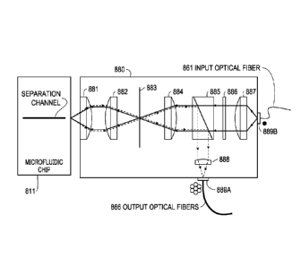
[0120] Fig. 7 shows a block diagram of an exemplary detection module 750
coupled
with an exemplary sample cartridge 715 having a microfluidic chip 711
according to an
embodiment of the disclosure. The detection module 750 can be suitably
installed in a DNA
analyzer, such as the DNA analyzer 100, or the DNA analyzer 400. Further, the
detection
module 750 can be coupled with other components, such as a processor 771. The
processor
771 processes signals received from the detection module 750 and provides
processed signals
to the detection module 750. The detection module 750 includes a light source
module 751,
an active optics module 753, and a detector 790. These elements are coupled
together using
optical fibers 761 and 766 as shown in Fig. 7.
CA 02814720 2013-04-12
WO 2012/051529 PCT/US2011/056357
24
[01211 In an embodiment, the microfluidic chip 711 includes generally
identical or
equivalent components as the exemplary microfluidic chip 311. For example, the
microfluidic chip 711 includes a first domain configured for PCR amplification
and a second
domain having a separation channel configured for electrophoretic separation.
In another
embodiment, the microfluidic chip 711 includes one or more separation channel
configured
for electrophoretic separation, and the microfluidic chip 711 does not
necessarily include the
first domain.
[0122] The detection module 750 is optically coupled to the microfluidic chip
711.
As described above, the microfluidic chip 711 includes a separation channel
configured for
electrophoretic separation of DNA fragments. The DNA fragments migrate in the
separation
channel based on their sizes. The DNA fragments can be suitably tagged with
fluorescent
labels. The fluorescent labels can be optically detected by the detection
module 750. Based
on the detected fluorescent labels, DNA analyses, such as identification,
sequencing, and the
like, can be suitably performed.
10123] More specifically, the detection module 750 directs a light beam to a
location of the separation channel along the migration direction of the DNA
fragments. The
light beam can excite the fluorescent labels attached to the DNA fragments to
emit
fluorescence when the DNA fragments migrate through the location. The
detection module
750 collects the emitted fluorescence and detects properties of the
fluorescence, such as
intensity, wavelength, timing, and the like. The detected properties can be
suitably stored and
analyzed.
[0124] The light source module 751 can include any suitable light emitting
device,
such as an argon-ion laser device, a solid state laser, a laser diode (LD),
and the like, to
generate the light beam. In an example, the light source module 751 includes a
Coherent
Sapphire optically pumped semiconductor laser (OPSL) that outputs a laser beam
of 488 nm
wavelength, and has an output power of 200 mW. The light source module 751
provides the
laser beam to the active optics module 753 via the input optical fiber 761.
[0125] In another example, the light source module 751 includes an LD that
emits
light in a wavelength range, such as in the wavelength range of 472 rim to 495
um. Further,
the light source module 751 includes a collimating lens (not shown), a filter
(not shown), and
a coupling lens (not shown). The collimating lens collimates the emitted light
from the LD.
Then, the filter, such as a low pass filter, blocks a portion of the spectra
that overlaps with
fluorescent labels in use. Further, the coupling lens couples the filtered
light to the input
CA 02814720 2013-04-12
WO 2012/051529 PCT/US2011/056357
optical fiber 761. The input optical fiber 761 provides an input light beam to
the active optics
module 753
[0126] It is noted that, in an embodiment, the input optical fiber 761 and the
light
beam transmitted by the input optical fiber 761 are suitably configured to
keep a relatively
small numerical aperture. In an example, the input optical fiber 761 and the
light beam
transmitted are configured to keep the numerical aperture smaller than 0.1,
such that the input
light beam is at a center of the active optics module 753 to minimize
aberration.
[0127] The active optics module 753 includes optical elements that may need to
be
adjusted for each sample cartridge 715. In the Fig. 7 example, the active
optics module 753
includes an optic assembly that includes a set of optic elements 780 and a
motion control
module 756 coupled to the set of optic elements 780 to move all or a portion
of the modular
component. The set of optic elements 780 is configured to receive the input
light beam from
the input optical fiber 761, and suitably directs the input light beam to the
separation channel
on the microfluidic chip 711. The set of optic elements 780 is also configured
to collect
fluorescence emitted by the fluorescent labels into an output light beam, and
transmit the
output light beam to the detector 790 via the output optical fibers 766. The
motion control
module 756 can adjust the set of optic elements 780 to align the set of optic
elements 780 to
the separation channel on the mierofluidic chip 711.
[0128] In the Fig. 7 example, the motion control module 756 receives signals
from
the processor 771 to move the set of optic elements 780. Thus, in an example,
the set of optic
elements 780, the detector 790, the processor 771 and the motion control
module 756 form a
loop during an optical calibration to align the set of optic elements 780 to
the separation
channel. For example, during an exemplary optical calibration process, a
specific dye, such
as a dye emitting light about 700 gm wavelength can be sent to a detection
zone of the
separation channel. The 700 pm wavelength is much larger than the fluorescent
labels
wavelength range (e.g., 530 nm to 650 nm), thus the dye does not interfere the
fluorescent
labels. The set of optic elements 780 directs the input light beam to the
separation channel to
stimulate the dye to emit light, and collects the resultant light emitted by
the dye. The set of
optic elements sends the emitted light to the detector 790 via the output
optical fibers 766. In
this exemplary optical calibration process, the detector 790 generates
electrical signals
corresponding to the light intensity of the emitted light. The processor 771
then signals the
motion control module 756 to position the set of optic elements 780 to
maximize the amount
of emitted light that the set of optic elements 780 receives.
CA 02814720 2013-04-12
WO 2012/051529 PCT/US2011/056357
26
[0129] In another example, a portion of the set of optic elements 780 has
adjustable
features. For example, an objective lens of the set of optic elements 780 has
adjustable focus.
In an embodiment, the objective lens is adjusted based on signals from the
processor 771 to
focus the input light beam onto the separation channel on the microfluidic
chip 711.
[0130] The detector 790 is configured to detect light properties of the output
light
beam, such as wavelength components, intensities corresponding to the
wavelength
components, and the like. In an embodiment, the detector 790 includes various
optical
elements (not shown) configured to cause spectral dispersion to spatially
separate the
wavelength components in the output light beam. Further, the detector 790
includes an array
of photo detection units to detect the spatially separated wavelength
components. In an
example, the optical elements include a dispersive element, such as a grating
element, to
cause spectral dispersion, and the detector 790 includes a charge coupled
device (CCD)
system to detect light intensities at different locations.
[0131] Generally, the light source module 751, and the detector 790 are
situated at
substantially fixed positions. In an example, the optical elements within the
detector 790 are
pre-calibrated and fixed at their calibrated positions by the manufacture.
Then, the optical
elements are situated at their calibrated positions, and do not need to be
adjusted for every
sample cartridge 715.
[0132] As shown, the detection module 750 can be implemented in a modular
manner. Each of the light source module 751, the detector 790 and the active
optics module
753 can be individually handled, such as manufactured, purchased, tested, and
calibrated.
Further, the light source module 751, the detector 790 and the active optics
module 753 can
be suitably coupled together using the input optical fiber 761 and the output
optical fibers
766, and assembled in a DNA analyzer. During operation, when a new sample
cartridge 715
is installed in the DNA analyzer, the active optics module 753 is calibrated
with regard to a
microfluidic chip 711 on the sample cartridge 715. The light source module 751
and the
detector 790 do not need to be adjusted for every sample cartridge 715.
[0133] In an example, when a new sample cartridge 715 is installed in a DNA
analyzer having the detection module 750, the DNA analyzer can start an
optical calibration
procedure to calibrate the detection module 750 with regard to a microfluidic
chip 711 on the
sample cartridge 715. During the calibration procedure, the motion control
module 756
aligns the set of optic elements 780 to a separation channel on the
microfluidic chip 711. In
an embodiment, a specific dye is sent into the separation channel to assist
the alignment. In
CA 02814720 2013-04-12
WO 2012/051529 PCT/US2011/056357
27
another example, the microfluidic chip 711 includes an alignment mark to
assist the set of
optic elements 780 to align to a desired location along the separation
channel.
[0134] In an embodiment, the DNA analyzer starts a control procedure to
control
the various components of the DNA analyzer to act on the microfluidic chip 711
in order to
perform an integrated single-chip DNA analysis. For example, template DNA can
be suitably
extracted and fluidically directed to the first domain of the microfluidic
chip 711; a PCR
amplification can be suitably induced in the first domain of the microfluidic
chip 711 to
amplify DNA fragments; then the amplified DNA fragments are suitably injected
into the
separation channel of the microfluidic chip 711; and then electrophoretic
separation can be
suitably induced in the separation channel. In addition, the detection module
750 can be
controlled to direct an input light beam to the separation channel to excite
fluorescent labels
used to tag the DNA fragments. The fluorescent labels emit fluorescence. The
detection
module 750 collects the fluorescence into an output light beam, and detects
fluorescence
information in the output light beam. The detected fluorescence information
can be suitably
stored, and further processed by the DNA analyzer, or can be transmitted to
other device for
further processing.
[0135] Fig. 8 shows an exemplary block diagram of a set of optic elements 880
according to an embodiment of the disclosure. The set of optic elements 880
includes a first
lens 881, a second lens 882, a pinhole 883, a third lens 884, a dichroic
mirror 885, a short
pass filter 886, a fourth lens 887 and a fifth lens 888 configured in a
confocal optical system.
The second lens 882, the pinhole 883 and the third lens 884 form a spatial
filter. Further, the
set of optic elements 880 are assembled together into an optic assembly. The
optic assembly
includes interfaces for coupling optical fibers with the set of optic elements
880. In the Fig. 8
example, the optic assembly includes a connector 889A for coupling output
optical fibers
866, and a connector 889B for coupling an input optical fiber 861. As shown,
the exemplary
connector 889A accepts seven optical fibers, arranges one optical fiber in the
center, and
arranges the other six optical fibers around the center optical fiber to form
a hexagon shape.
The connector 889B accepts one optical fiber. It should be understood that the
connector
889B can include more than one optical fiber, and the connector 889A can
include other
numbers of optical fibers, and can arrange the optical fibers in various
different shape.
[0136] The set of optic elements 880 fowls an input optical path (illuminating
path)
and an output optical path (detecting path). The input optical path includes
the input optical
fiber 861, the fourth lens 887, the short pass filter 886, the dichroic mirror
885, the third lens
CA 02814720 2013-04-12
WO 2012/051529 PCT/US2011/056357
28
884, the pinhole 883, the second lens 882, and the first lens 881. The output
optical path
includes the first lens 881, the second lens 882, the pinhole 883, the third
lens 884, the
dichroic mirror 885, and the fifth lens 888.
[0137] On the input optical path, the input optical fiber 861 emits the input
light
beam into the set of optic elements 880. The fourth lens 887 forms the input
light beam into
a substantially collimated light beam. The short pass filter 886 reduces
fluorescence
components in the collimated input light beam. In an embodiment, the input
optical fiber 861
generates auto-fluorescence. The auto-fluorescence is a relatively large
portion of noise to
the whole system. The short pass filter 886 reduces the auto-fluorescence in
the collimated
input light beam to improve signal to noise ratio.
[0138] The dichroic mirror 885 is configured to allow the filtered collimated
input
light beam to pass. Then, the third lens 881 forms the filtered collimated
light beam into a
narrowing conical input beam that is focused to pass the pinhole 883.
[01391 Then, the conical input beam passes the second lens 882 and the first
lens
881. The second lens 882 collimates the conical input light beam, and the
first lens 881
focuses the input light beam onto a detection zone of the separation channel.
[01401 When DNA fragments migrate to the detection zone of the separation
channel, the fluorescence labels attached on the DNA fragments absorb the
input light beam,
and emit fluorescence.
[0141] On the output optical path, the first lens 881 collects the
fluorescence
emitted from the fluorescence labels, and forms collimated output light beam.
Then, the
second lens 882 forms the collimated output light beam into a narrowing
conical output beam
that is focused to pass the pinhole 883. The spatial filter formed by the
second lens 882, the
pinhole 883 and the third lens 884 rejects scattered light from surrounding
surfaces into the
microfluidic chip. Then, third lens 884 collimates the conical output light
beam. The
dichroic mirror 885 reflects the collimated output light beam to direct the
output light beam to
the fifth lens 888. The fifth lens 888 focuses the output light beam to the
output optical fibers
866 connected on the connector 889A.
[0142] It is noted that, in the Fig. 8 example, the input optical path and the
output
optical path do not completely overlap due to the dichroic mirror 885. Thus,
different optical
elements can be used on the input optical path and the output optical path to
suit for different
needs of the two optical paths. This configuration provides flexibility, and
different optics
can be added on the two optical paths to improve performance. For example, the
short pass
CA 02814720 2013-04-12
WO 2012/051529 PCT/US2011/056357
29
filter 886 is used on the input optical path to reduce auto-fluorescence
generated by input
optical fiber 861.
10143] Fig. 9 shows a block diagram of another set of optic elements example
980
according to an exemplary embodiment of the disclosure. The set of optic
elements 980
includes a first lens 981, a second lens 982, a pinhole 983, a third lens 984,
and a fourth lens
987 configured in a confocal optical system. The second lens 982, the pinhole
983 and the
third lens 984 form a spatial filter. Further, the set of optic elements 980
includes a connector
989 for coupling both an input optical fiber 961 and output optical fibers
966. The connector
989 is configured to arranges the input optical fiber 961 in the center, and
arranges six output
optical fibers 966 around the center optical fiber to form a hexagon shape.
[0144] The set of optic elements 980 forms an input optical path (illuminating
path)
and an output optical path (detecting path) using the same optics. The input
optical path
follows the input optical fiber 961, the fourth lens 987, the third lens 984,
the pinhole 983, the
second lens 982, and the first lens 981. The output optical path follows the
first lens 981, the
second lens 982, the pinhole 983, the third lens 984, and the fourth lens 987.
[0145] On the input optical path, the input optical fiber 961 emits the input
light
beam into the set of optic elements 980. In an example, the input optical
fiber 961 and the
light transmitted in the input optical fiber 961 are configured to have a
relatively small
numerical aperture, such as smaller than 0.1. Thus, the input light emitted by
the input
optical fiber 961 keeps in the center of the optics in the set of optic
elements 980 to reduce
aberration.
[0146] The fourth lens 987 forms the input light beam into a substantially
collimated light beam. Then, the third lens 981 forms the filtered collimated
light beam into
a narrowing conical input beam that is focused to pass the pinhole 983.
10147] Then, the conical input beam passes the second lens 982 and the first
lens
981. The second lens 982 collimates the conical input beam, and the first lens
981 focuses
the input light beam onto a detection zone of the separation channel.
[0148] When DNA fragments migrate to the detection zone of the separation
channel, the fluorescence labels attached to the DNA fragments absorb the
input light beam,
and emit fluorescence.
[0149] On the output optical path, the first lens 981 collects the
fluorescence
emitted from the fluorescence labels, and forms collimated output light beam.
It is noted that
the fluorescence labels may emit the fluorescence in all directions. In an
embodiment, the
CA 02814720 2013-04-12
WO 2012/051529 PCT/US2011/056357
first lens 981 has a relatively large numerical aperture, such as greater than
0.5 to collect a
relatively large portion of the fluorescence. Then, the second lens 982 forms
the collimated
output light beam into a narrowing conical output light beam that is focused
to pass the
pinhole 983. The spatial filter formed by the second lens 982, the pinhole 983
and the third
lens 984 rejects scattered light from surrounding surfaces. Then, third lens
984 collimates the
conical output light beam. The fourth lens 987 focuses the output light beam
to the optical
fibers 966 and 961 attached to the connector 989.
[0150] It is noted that, in an embodiment, the fourth lens 987 can be suitably
configured that a relatively larger portion of the output light beam, such as
more than 50% of
the output light beam, can be aberrated onto the output optical fibers 966.
[0151] Fig. 10 shows a block diagram of a detector example 1090 according to
an
exemplary embodiment of the disclosure. The detector 1090 includes first
lenses 1092, a
dispersive element 1093, second lenses 1094, and a CCD system 1098. Further,
the detector
1090 includes a connector 1091 configured to couple optical fibers 1066 with
the detector
1090.
[0152] In an embodiment, the optical fibers 1066 include two ends. Each end is
attached to a suitable connector. hi the Fig. 10 example, one end of the
optical fibers 1066 is
attached to the connector 1091 and the other end of the optical fibers 1066 is
attached to a
connector 1089. The connector 1089 and the connector 1091 are in different
configurations.
In the Fig. 10 example, the optical fibers 1066 are in the folin of a bundle
of seven optical
fibers. The connector 1089 arranges one optical fiber in the center, and
arranges the other six
optical fibers around the center optical fiber to form a hexagon shape. The
connector 1091
stacks the seven optical fibers vertically to form a vertical slit.
[0153] During operation, the optical fibers 1066 transmit a light beam having
the
collected fluorescence from the connector 1089 to the connector 1091. The
optical fibers
1066 emit the light beam in the form of a vertical line. The first lenses 1092
collectively
collimate the light beam. In an example, the dispersive element 1093 is a
grating element that
has a large number of closely spaced vertical slits constituting a grating.
The dispersive
element 1093 causes spectral dispersion to spatially spread the fluorescence
components by
wavelengths. It is noted that, for ease of illustration, the spectral
dispersion onto a detection
surface of the CCD system 1098 is shown in the horizontal direction. The
second lenses
1094 collectively focus the spread fluorescence components onto the CCD system
1098 at
different horizontal locations. The CCD system 1098 includes an array of photo
sensitive
CA 02814720 2013-04-12
WO 2012/051529 PCT/US2011/056357
31
devices configured to detect light intensities at the different horizontal
locations. The light
intensities, and the location information can be used to identify fluorescence
labels, and
identify DNA fragments.
10154] Fig. 11 shows a schematic diagram of a multiple-sample microfluidic
chip
example 1100 according to an embodiment of the disclosure. The multiple-sample
microfluidic chip 1100 can be used to simultaneously perform DNA analysis for
multiple
samples. Similar to the microfluidic chip 311 in Fig. 3, the multiple-sample
microfluidic chip
1100 includes various micro structures, such as inlets 1121-1124, reaction
reservoirs 1152,
1162 and 1172, connection channels 1151,1161, 1171, 1181, 1153, 1163 and 1173,
injection
channels 1154, 1164, 1174 and 1184, separation channels 1155, 1165, 1175 and
1185
(separation channel-A to separation channel-D), electrode reservoirs 1131-
1140, waste
reservoirs 1124 and 1125, and the like. These micro structures can be
similarly configured as
their corresponding micro structures in Fig. 3 and can operate similarly as
their corresponding
micro structures in Fig. 3.
[0155] In addition, similar to the microfluidic chip 311, the multiple-sample
microfluidic chip 1100 includes a first domain 1111a, and a second domain
1111b. The first
domain 1111a is a thermal control domain, and the temperature within the first
domain 1111a
can be controlled in a similar manner as the thermal control domain 311 a.
[0156] The first domain 1111a can include multiple reaction reservoirs that
are
respectively designated to multiple samples to perform simultaneous PCR
amplification for
the multiple samples. In the Fig. 11 example, the reaction reservoirs 1152,
1162 and 1172 are
located within the first domain 1111a. During a PCR amplification step, for
example, the
reaction reservoir 1152 includes a first liquid mixture of a first template
DNA extracted from
a first sample and first reagents, the reaction reservoir 1162 includes a
second liquid mixture
of a second template DNA extracted from a second sample and second reagents,
and the
reaction reservoir 1172 includes a third liquid mixture of a third template
DNA extracted
from a third sample and third reagents. Then, when thermal cycles are
generated within the
first domain 1111a, for example, by an infrared light source and a cooling
fan, PCR
amplifications can be simultaneously performed in the reaction reservoirs
1152, 1162 and
1172.
[0157] In an embodiment, the first domain 1111a includes a thermal coupler
reservoir (not shown) for measuring a temperature within the first domain
1111a. In another
embodiment, the temperature measurement is performed by an infrared sensing
unit.
CA 02814720 2013-04-12
WO 2012/051529 PCT/US2011/056357
32
[0158] The second domain 1111b includes multiple separation units that are
respectively designated to multiple samples. In an embodiment, each separation
unit includes
a separation channel and an injection channel coupled together. In addition,
the separation
unit includes electrode reservoirs that are in association with the injection
channel and the
separation channel to provide electric fields for electro-kinetic injection
and electrophoretic
separation. It is noted that separation units may share electrode reservoirs.
In the Fig. 11
example, the second domain 1111b includes four separation units. The first
separation unit
includes the injection channel 1154 and the separation channel 1155. The
second separation
unit includes the injection channel 1164 and the separation channel 1165. The
third
separation unit includes the injection channel 1174 and the separation channel
1175. The
fourth separation unit includes the injection channel 1184 and the separation
channel 1185.
[0159] It is noted that the multiple-sample microfluidic chip 1100 can include
other
domains, such as post-PCR clean-up/dilution domain, and the like.
Alternatively, a domain
can be configured to be a multi-purpose domain. For example, the first domain
1111a can be
suitably configured for purification and/or post-PCR processing. Thus, the
reaction reservoirs
1152, 1162 and 1172 can also be purification reservoirs and/or post-PCR
reservoirs.
[0160] In another example, the electrode reservoirs 1131, 1133 and 1136 are
suitably configured for diluting PCR mixtures. Specifically, the electrode
reservoir 1131
dilutes a first PCR mixture received from the reaction reservoir 1152 with a
first dilutant, and
prepares the first PCR mixture for electrophoretic separation in the
separation channel 1155.
The electrode reservoir 1133 dilutes a second PCR mixture received from the
reaction
reservoir 1162 with a second dilutant, and prepares the second PCR mixture for
electrophoretic separation in the separation channel 1165. The electrode
reservoir 1136
dilutes a third PCR mixture received from the reaction reservoir 1172 with a
third dilutant,
and prepares the third PCR mixture for electrophoretic separation in the
separation channel
1175. In an embodiment, respective dilution ratios are used in the electrode
reservoirs 1131,
1133 and 1136. The dilution ratios are from 1:5 to 1:20 (one part of PCR
mixture to 5-20
parts of dilutant).
[0161] The various micro structures can be suitably coupled together to form
multiple processing units for multiple-sample DNA analysis. In Fig. 11
example, the
multiple-sample microfluidic chip 1100 includes four processing units. The
first processing
unit includes the inlets 1121, the connection channel 1151, the reaction
reservoir 1152, the
connection channel 1153, the injection channel 1154, and the separation
channel 1155. The
CA 02814720 2013-04-12
WO 2012/051529 PCT/US2011/056357
33
second processing unit includes the inlets 1122, the connection channel 1161,
the reaction
reservoir 1162, the connection channel 1163, the injection channel 1164, and
the separation
channel 1165. The third processing unit includes the inlets 1123, the
connection channel
1171, the reaction reservoir 1172, the connection channel 1173, the injection
channel 1174,
and the separation channel 1175. The fourth processing unit includes the inlet
1124, the
connection channel 1181, the injection channel 1184, and the separation
channel 1185.
[0162] The micro structures of a processing unit can be fluidically coupled
together
to enable liquid flow. Using the first processing unit as an example, the
inlets 1121 are
suitably coupled to a pump module. The pump module can input the first
template DNA and
the first reagents into the reaction reservoir 1152 via the connection channel
1151 by a
pressure force. In the reaction reservoir 1152, PCR amplification is performed
based on the
first template DNA and the first reagents. After the PCR amplification, the
DNA amplicons
flow through the connection channel 1153 by a pressure force. Further, the DNA
amplicons
are injected into the separation channel 1155 via the injection channel 1154
by an electro-
kinetic force. Then, electrophoretic separation can be performed in the
separation channel
1155.
[01631 The multiple processing units can be configured to fluidically
separated from
each other on the same multiple-sample microfluidic chip 1100. Thus, the
multiple
processing units can be respectively used to perform DNA analysis for multiple
samples
using a single microfluidic chip.
[0164] It is noted that the processing units can be suitably configured to
include
branches. The branches can be suitably enabled or disabled. Using the first
processing unit
in Fig. 11 as an example, in addition to the connection channel 1153, the
reaction reservoir
1152 is also coupled to a connection channel 1156 directing to the waste
reservoir 1124. In
an embodiment, the connection channel 1153 has a higher resistance than the
connection
channel 1156, for example, by having a smaller cross-section area than the
connection
channel 1156. However, the connection channel 1156 includes a valve 1157. When
the
valve 1157 is closed, the connection channel 1156 is closed, then liquid can
be forced to the
higher resistance connection channel 1153. When the valve 1157 is open, liquid
can flow
through the connection channel 1156 to the waste reservoir 1124.
[0165] It is also noted that the four processing units can be configured in a
same
manner or can be configured in different manners. In the Fig. 11 example, the
first, second
and third processing units are configured in a same manner, and the fourth
processing unit is
CA 02814720 2013-04-12
WO 2012/051529 PCT/US2011/056357
34
configured differently from the other processing units. For example, each of
the first, second
and third processing units includes a reaction reservoir in the first domain
1111a. In addition,
corresponding connection channels, such as the connection channels 1153, 1163
and 1173,
are suitably routed, such as zigzagged, to have substantially the same length.
Thus, the first,
second and third processing units can be used to perform DNA analysis for
three samples
simultaneously. The fourth processing unit does not include a reaction
reservoir in the first
domain 1111a. Thus, the fourth processing unit can be used to perform DNA
analysis for a
sample that does not need PCR amplification, or the PCR amplification for the
sample is
suitably perfollued previously.
[0166] It is also noted that a multiple-sample microfluidic chip can include
multiple
first domains, and/or second domains. In an example, a multiple-sample
microfluidic chip
may suitably include four sets of the schematic diagram in Fig. 11. Then, the
multiple-sample
microfluidic chip can be used to simultaneously perform DNA analysis for
twelve samples, or
can be used to simultaneously perfollil electrophoretic separation for sixteen
samples.
[0167] Of course, a multiple-sample microfluidic chip can be configured to
repeat
the structure in a single sample microfluidic chip, such as the microfluidic
chip 311. The
repeated structures may be coupled together, or may be independent of each
other. In an
example, two structures are thermally coupled together. For example, the PCR
reaction
reservoirs of the two structures are thermally coupled together. In another
example, two
structures are fluidically coupled together. For example, the two structures
share a same inlet.
In another example, the repeated structures are independent of each other. For
example, the
PCR reaction reservoirs of the repeated structures are thermally isolated,
thus thermal cycles
can be independently induced for the PCR reaction reservoirs.
[0168] Accordingly, a DNA analyzer can be suitably configured for multiple-
sample
DNA analysis. For example, a thermal module of the DNA analyzer has a
capability to
generate thermal cycles within multiple first domains on a multiple-sample
microfluidic chip,
and the thermal module can be suitably configured to suit a multiple-sample
microfluidic chip
in use. In an embodiment, a thermal module of the DNA analyzer includes a
halogen light
bulb to direct heat to a first domain, such as the first domain 1111a,
including multiple
thermally coupled reaction reservoirs for PCR amplification. In another
embodiment, a
thermal module of the DNA analyzer includes multiple heat sources that can
independently
direct heat to thermally isolated reaction reservoirs. In another example, a
detection module
of the DNA analyzer has a capability to detect fluorescence from sixteen
separation channels.
CA 02814720 2013-04-12
WO 2012/051529 PCT/US2011/056357
The detection module can be suitably configured to suit a multiple-sample
microfluidic chip
in use.
10169] Fig. 12 shows a block diagram of an exemplary detection module 1250
coupled with an exemplary sample cartridge 1215 having a microfluidic chip
1200 according
to an embodiment of the disclosure. The detection module 1250 can be suitably
installed in a
DNA analyzer, such as the DNA analyzer 100, or the DNA analyzer 400. Further,
the
detection module 1250 can be coupled with other components, such as a
processor 1271. The
detection module 1250 includes a light source module 1251, an active optics
module 1253,
and a detector 1290. These elements are coupled together using optical fibers.
[0170] The microfluidic chip 1200 includes multiple separation channels, for
example, separation channel-A to separation channel-D. The multiple separation
channels
can be configured to perform, in parallel, electrophoretic separation of
multiple DNA
samples. In an embodiment, the microfluidic chip 1200 is configured
identically or
equivalently to the microfluidic chip 1100 to simultaneously perform
integrated DNA
analysis for multiple samples; the description of these components has been
provided above
and will be omitted here for clarity purposes. In another embodiment, the
microfluidic chip
1200 includes the multiple separation channels and other suitable structures
to merely
perform electrophoretic separation of multiple DNA samples.
101711 The detection module 1250 utilizes certain components that are
identical or
equivalent to those used in the detection module 750; the description of these
components has
been provided above and will be omitted here for clarity purposes. However, in
this
embodiment, the active optics module 1253 includes multiple optic assemblies,
and each
optic assembly includes a set of optic elements and a motion control module.
For example, a
first optic assembly includes a set of optical elements 1280-A and a motion
control module
1256-A; a second optic assembly includes a set of optical elements 1280-B and
a motion
control module 1256-B; a third optic assembly includes a set of optical
elements 1280-C and
a motion control module 1256-C; and a fourth optic assembly includes a set of
optical
elements 1280-D and a motion control module 1256-D.
[0172] The light source module 1251 can include any suitably light emitting
device,
such as an argon-ion laser device, a solid state laser, a laser diode (LD),
and the like, to
provide light beams to the multiple optic assemblies. In an example, the light
source module
1251 includes a laser module, such as a Coherent Sapphire optically pumped
semiconductor
laser (OPSL) outputting a laser beam of 488 nm wavelength. Further, the light
source module
CA 02814720 2013-04-12
WO 2012/051529 PCT/US2011/056357
36
1251 includes a splitter configured to split the laser beam into multiple
laser beams. The
multiple laser beams are respectively provided to the multiple optic
assemblies via the input
optical fiber-A to input optical fiber-D.
[01731 In another example, the light source module 1251 includes multiple sets
of
LDs coupled with suitable optic elements to generate the multiple input light
beams. The
multiple light beams are respectively provided to the multiple optic
assemblies via the input
optical fiber-A to input optical fiber-D.
[0174] Each optic assembly in Fig. 12 utilizes certain components that are
identical
or equivalent to those used in the optic assembly in Fig. 7; the description
of these
components has been provided above and will be omitted here for clarity
purposes. Each
optic assembly receives an input light beam from the light source module 1251
via an input
optical fiber, and provides an output light beam to the detector 1290 via a
group of output
optical fibers.
[01751 The detector 1290 utilizes certain components that are identical or
equivalent to those used in the detector 1090; the description of these
components has been
provided above and will be omitted here for clarity purposes. However, in an
embodiment,
the connector 1291 stacks all the output optical fibers in the four groups of
output optical
fibers vertically with space between groups to form a broken vertical slit.
Specifically, the
connector 1291 stacks optical fibers within a group together vertically as the
connector 1091,
and stacks the four groups vertically with space between groups. Thus, each
section in the
broken vertical slit corresponds to an output light beam collected from a
separation channel.
In an example, the dispersive element 1293 is a grating element that has a
large number of
closely spaced vertical slits constituting a grating. The dispersive element
1293 causes
spectral dispersion to spatially spread fluorescence components in the broken
vertical slit by
wavelengths. It is noted that, for ease of illustration, the spectral
dispersion onto a detection
surface of the CCD system 1298 is shown in the horizontal direction. The
spread
fluorescence components are imaged onto the CCD system 1298 at different
horizontal
locations. The CCD system 1298 includes an array of photo sensitive devices
configured to
detect light intensities at the different horizontal locations and vertical
regions. The vertical
region information can be used to identical separation channels, and the light
intensities, and
the horizontal location information can be used to identify fluorescence
labels and to identify
DNA fragments.
CA 02814720 2013-04-12
WO 2012/051529 PCT/US2011/056357
37
[0176] It is noted that, in another embodiment, the connector 1291 may stack
all the
output optical fibers in the four groups of output optical fibers vertically
in a line without any
space between the groups.
101771 While the invention has been described in conjunction with the specific
embodiments thereof that are proposed as examples, it is evident that many
alternatives,
modifications, and variations will be apparent to those skilled in the art.
Accordingly,
embodiments of the invention as set forth herein are intended to be
illustrative, not limiting.
There are changes that may be made without departing from the scope of the
invention.