Note: Descriptions are shown in the official language in which they were submitted.
CA 02816180 2015-05-26
WO 03/105063
PCT/US03/01513
RFID LABEL TECHNIQUE
10001]
BACKGROUND OF THE INVENTION
FIELD OF THE INVENTION
[0002] This invention relates to the field of Radio Frequency Identification
(RFID) tags
and labels, and to particular methods of manufacturing them, including a roll-
to-roll
method of manufacture and an alternative sheet-to-roll method of manufacture.
PRIOR ART
[0003] RFID tags and labels have a combination of antennas and analog and/or
digital
electronics, which may include for example communications electronics, data
memory,
and control logic. RFID tags and labels are widely used to associate an object
with an
identification code. For example, RFID tags are used in conjunction with
security-locks
in cars, for access control to buildings, and for tracking inventory and
parcels. Some
examples of RFID tags and labels appear in U.S. Patent Nos. 6,107,920:
6,206,292; and
6,262,292, all of which this application incorporates by reference.
[0004] RFID tags and labels include active tags, which include a power source,
and
passive tags and labels, which do not. In the ease of passive tags, in order
to retrieve the
information from the chip, a "base station" or "reader" sends an excitation
signal to the
RFID tag or label. The excitation signal energizes the tag or label, and the
RFID circuitry
transmits the stored information back to the reader. The "reader" receives and
decodes
the information from the RFID tag. In general, RFID tags can retain and
transmit enough
information to uniquely identify individuals, packages, inventory and the
like. RFID tags
and labels also can be characterized as to those to which information is
1
CA 02816180 2015-01-05
W003/105063 PM/UM/01513
written only once (although the information may be read repeatedly), and those
to which
information may be written during use. For example, REID tags may store
environmental data (that may be detected by an associated sensor), logistical
histories,
state data, etc.
100051 Methods for manufacturing REID labels are disclosed in POT Publication
No.
WO 01/61646 by Moore North America, Inc. The
method disclosed in PCT Publication No. WO 01/61646 uses a number of different
sources of REID inlets, each inlet including an antenna and a chip. A
plurality of webs
are matched together and REID labels are die cut from the webs, to produce RFD
labels with liner. Alternatively, fineness REID labels are produced from a
composite
web with a release material on one face and pressure sensitive adhesive on the
other,
the labels formed by perforations in the web, Various alternatives are
possible.
100061 Still other REID devices and methods for manufacturing REM labels are
disclosed in United States Patent Application Publication No. US2001/0053675
by
Piettner. The devices include a transponder
comprising a chip having contact pads and at least two coupling elements,
which are
conductively connected with the contact pads. The coupling elements are touch-
free
relative to each other and formed in a self-supported as well as a free-
standing way and
are essentially extended parallel to the chip plane. The total mounting height
of the
transponder corresponds essentially to the mounting height of the chip. The
size and
geometry of the coupling elements are adapted for acting as a dipole antenna
or in
conjunction with an evaluation unit as a plate capacitor. Typically, the
transponders are
produced at the wafer level. The coupling elements can be contacted with the
contact
pads of the chip directly at the wafer level, i.e., before the chips are
extracted from the
grouping given by the wafer.
[0007] In many applications, it is desirable to reduce the size of the
electronics as
small as possible. Applicants' assignee Avery Dennison Corporation has been
working
with Alien Technology Corporation and others to identify materials, devise
constructions, and develop processing techniques to efficiently produce rolls
of a
flexible substrate filled with 'small electronic blocks*.
2
CA 02816180 2015-01-05
WO 03/105063 PCF/1J803/01513
MOM Considering the flexible substrate filled with "small electronic blocks,"
Alien
Technology Corporation ("Men"), of Morgan Hill, California, for example, has
developed
techniques for manufacturing microelectronic elements as small electronic
blocks, which
Alien calls "NanoBlocks", and then depositing the small electronic blocks into
recesses
on an underlying substrate. To receive the small electronic blocks, a planar
substrate
200 (Fig. 1) is embossed with numerous receptor wells 210. The receptor wells
210 are
typically formed in a pattern on the substrate. For instance, in Fig. 1 the
receptor wells
210 form a simple matrix pattern that may extend over only a predefined
portion of the
substrate, or may extend across substantially the entire width and length of
the
substrate, as desired.
[00091 To place the small electronic blocks into the recesses, Alien uses a
technique
known as Fluidic Self Assembly ("FSA"). The FSA method includes dispersing the
small electronic blocks in a slurry, and then flowing the slurry over the top
surface of the
substrate. The small electronic blocks and recesses have complementary shapes,
and
gravity pulls the small electronic blocks down into the recesses. The end-
result is a
substrate (e.g., a sheet, a web, or a plate) that is embedded with tiny
electronic
elements. Fig. 2 illustrates a small electronic block 100 disposed within a
recess 210.
Between the block 100 and the substrate 220 is a metallization layer 222. The
block
100 has a top surface with a circuit 224 disposed thereon.
00101 Alien has a number of patents on its technique, including U.S. Patent
Nos.
6,783,866; 5,824,186; 5,904,545; 5,545,291; 6,274,508; and 6,281,036.
Further information can be found in
Allen's Patent Cooperation Treaty publications, including WO 00/49421; WO
00/49658;
WO 00/55915; WO 00/55916; WO 00/46854 and WO 01/33621.
Other recent publications of interest appeared in
the Information Display, Nov. 2000, Vol. 16, No. 11 at pp. 12-17, and in a
paper
published by the MIT Auto-ID Center, entitled, 'Toward the 5 Cent Tag,"
published In
February 2002, Further details regarding the manufacture of the microstructure
elements and the FSA processes may be found in U.S. Patents 6,545,291 and
5,904,545, and in PCT/1JS99/30391 at WO 00/46854
3
CA 02816180 2013-05-16
WO 03/105063 PCT/US03/01513
[0011] As set forth in the MIT Auto-ID Center publication cited above, the
electronic
blocks may be located in the openings by a vibratory feeder assembly, such as
that
developed by Philips, instead of the Fluidic Self-Assembly method.
Alternatively, the
electronic blocks may be located into the openings with a deterministic pick
and place
method, which can use a robot arm to pick the electronic elements and place
them one
at a time into respective openings, as described in U.S. Patent No. 6,274,508.
[0012] In yet another approach to locating the electronic blocks, the webstock
or
sheetstock may include openings that extend through the entire thickness of
the sheet.
A vacuum may be applied below the webstock to pull the electronic blocks into
and to fill
the openings.
[0013] The present invention addresses a significant need in these methods
involving
the placement of small electronic blocks or chips in openings of a flexible
substrate, as
well as in more conventional surface mounting techniques for placing chips on
flexible
substrates. That is, it can be desirable to space the chips at densities
exceeding the
densities of antennas to which the chips later are bonded, e.g. antennas
formed on
webstock. The present invention provides this capability, furthermore, using
techniques
well suited to high speed roll-to-roll production of RFID tags and labels.
SUMMARY OF THE INVENTION
[0014] This invention relates to methods of making articles for RFID (Radio
Frequency
Identification), such as tags or labels. These methods process flexible
webstock or
sheetstock with embedded or surface mounted chips ¨ herein called "RFID
webstock"
or "RFID sheetstock", respectively.
[0015] As used in this patent application, the "pitch" of elements on a
webstock or
sheetstock (such as chips within an RFID webstock, or labels within a label
stock)
means the center-to-center distance between adjacent elements. In the present
invention, the pitch of chips may be different than the pitch of an array of
RFID tags or
labels to be formed: (a) in the longitudinal (also called the "down web")
direction; (b) in
the transverse (or "cross web") direction, or (c) in both directions. As used
in the
present patent application, the "pitch density", or the number per unit area
e.g. of chips,
is determined by calculating the reciprocal of the product of these pitches.
4
CA 02816180 2013-05-16
WO 03/105063 PCT/US03/01513
[0016] In accordance with one aspect of the roll-to-roll manufacturing method,
the
pitch density of the chips in RFID webstock or RFID sheetstock is different
from
(preferably significantly greater than) the pitch density of the individual
RFID tags or
labels within the roll of tags or labels. The difference in pitch density
results from a
difference in pitch in the down-web direction, in the cross-web direction, or
in both
directions. Typically the pitch of the chips along each axis of the RFID
webstock is less
than or equal to the pitch of antennas along the corresponding axis of the
antenna web.
This difference in chip density is attributable to the separation of the RFID
webstock into
"sections", and the adjustment of pitch density ("indexing") of these sections
in the roll-
to-roll lamination process. In one embodiment, the RFID webstock is die cut
into a
series of sections each containing a cross web column of chips, and the down-
web pitch
of chips is increased prior to lamination of the sections to a web containing
antennas to
form an RFID inlay stock. In another embodiment, the RFID webstock is die cut
into a
series of sections each comprising a lane containing a down-web row of chips,
and
these lanes are then spread or separated to increase the cross-web pitch of
chips prior
to lamination of the sections to a web containing antennas. In a third
embodiment, an
RFID webstock is first slit into lanes, and then individual sections are cut
or separated
from each lane in order to adjust the down-web pitch of the individual chip
sections.
[0017] The method of the invention is adapted both to the use of RFID webstock
and
RFID sheetstock as a carrier for RFID chips, the former being highly
preferred. The
term "RFID microelectronic stock" is used to encompass both RFID webstock and
RFID
sheetstock. These terms identify the webstock or sheetstock including RFID
chips and
electrical connectors, but before joining to antennas. Once the individual
chips are
associated with corresponding antennas, this patent application uses "RFID
inlay" to
identify individual chip-antenna assemblies, and the term "RFID inlay stock"
to identify a
webstock containing such RFID inlays.
[0018] In a preferred embodiment, the pitch density of the chips in the RFID
inlay stock
is the same as the pitch density of the chips in the final tag or label stock.
However, it is
possible further to adjust the pitch density of the individual RFID inlays and
chips as
they are integrated into the final tag or label stock.
CA 02816180 2013-05-16
WO 03/105063 PCT/US03/01513
[0019] According to one embodiment of the invention, a method of forming an
RFID
article includes providing an RFID webstock having a plurality of recesses,
each of the
recesses containing an RFID chip. A second web is provided having antennas
spaced
thereon. The RFID webstock is divided (e.g. severed, or separated) into a
plurality of
sections, each of the sections including one or more of the RFID chips. The
pitch of the
RFID sections is indexed from a high pitch density on the RFD webstock, to a
relatively
low pitch density on an RFID inlay stock. The sections are attached to a
plurality of
antennas in an automatic continuous process, so that each of the RFID chips is
joined
to (placed in ohmic communication with) one of the antennas to form an RFID
inlay
stock.
[0020] According to another embodiment of the invention, a method of forming
an
RFID article includes providing an RF1D webstock of polymeric material having
an array
of RF1D chips. A second web is provided having antennas spaced thereon. The
RFID
webstock is divided into a plurality of sections, each of the sections
including one or
more of the RFID chips. The pitch of the RFID sections is indexed from a
relatively high
density on the RFID webstock, to a relatively low density on an RFID inlay
stock. The
sections are attached to a plurality of antennas in an automatic continuous
process, so
that each of the RFID chips is adjacent to one of the antennas to form an RFID
inlay
stock.
[0021] According to other embodiments, the dividing and indexing steps may be
effected using a cutter member and a transport member, the RFID webstock being
passed through a cutting location between the cutter member and transport
member,
wherein sections are cut from the RFID webstock and engaged by the transport
member. The transport member may convey sections from the cutting location to
a
transfer location at which each of the sections is joined to an antenna. The
cutter
member and transport member may be, for example, rollers or belts. The
transport
member may engage sections with vacuum holders or clamps.
[0022] In the indexing step the down-web spacing of RFID chips on the RFID
webstock may be increased on the transport member, to match the spacing of
antennas
to which these chips are joined at the transfer location. The indexing step
may further
6
CA 02816180 2013-05-16
WO 03/105063 PCT/US03/01513
include the step of transporting the RFID webstock so as to effect indexing of
the down-
web pitch of the RFID chips relative to the pitch of these chips on the
transport member.
[0023] A step of indexing in the cross-web direction may be done by, for
example,
slitting the RFID webstock of polymeric material into lanes, and spreading the
lanes
apart. The lanes once separated can travel along diverging paths, or can be
realigned
to be travel along parallel paths (of increased cross-web pitch in comparison
to the
original cross-web pitch).
[0024] Another embodiment of the indexing step is to divide the RFID webstock
into a
series of cross-web columns of chips, which can be engaged on the transport
member
and indexed separately from other columns of chips.
[0025] The attaching step may be effected by pressing the transport member
against a
lamination member at the transfer location, at which the section and antenna
web pass
through a nip or an extended zone of contact between the transport member and
lamination member. For example the transport member and lamination member may
both comprise two rollers, or a roller and a belt, or two belts.
[0026] In another specific embodiment, the method may further comprise
unrolling a
first facestock roll and laminating the first facestock roll to the RFID inlay
stock. A
second roll of facestock may be unwound, and the facestock from the second
roll may
be attached to the RFD inlay stock opposite the first facestock. The method
may
further include the step of forming an adhesive label.
10027] The antennas may be formed in any of a number of different ways such
as, for
example, (i) printing conductive ink; (ii) sputtering metal; (iii) laminating
foil; and (iv) hot-
stamping.
[0028] Considering aspects of the invention further, in one embodiment of a
converting
assembly to separate RFID sections and join them to antennas, the RFID
webstock is
severed into sections by passing the webstock through a cutting location
between a
cutter member and a transport member. Preferably, the transport member acts as
an
anvil as sections are cut from the RFID webstock. In one embodiment, the
transport
member and cutter member are rollers; alternatively one or both of these
members may
comprise a belt. The transport member may include holders for engaging the cut
sections, such as vacuum holders or clamps. The transport member conveys the
7
CA 02816180 2013-05-16
WO 03/105063 PCT/US03/01513
sections from the cutting location to a transfer location, at which the
sections are joined
to antennas to form RFID inlay stock. Preferably the antennas are carried on a
webstock.
[0029] In the preferred operation of this converting assembly, the transport
of the RFID
webstock, the operation of the cutter member, and the engagement of the
sections by
the transport member, are controlled so as to increase the pitch of the RFID
chips from
a relatively narrow pitch to a relatively wide pitch. Preferably the
converting assembly
increases the down-web spacing of the chips. In one embodiment, the transport
of the
RFID webstock may include a shuttle that induces periodic forward and
retrograde
motions of the RFID webstock. Preferably, the motion of the transport member
at the
transfer location matches the motion of an antenna-carrying webstock, to
register the
sections with respective antennas.
[0030] This converting assembly may act upon an RFID webstock containing a
single
lane of chips (which may have been slit from a webstock with a plurality of
lanes of
chips). In this case, a plurality of such converting assemblies would be
provided, one
for each lane of chips. Alternatively, the converting assembly may act upon
webstock
containing a plurality of lanes, wherein each severed section would include a
cross-web
column of chips.
[0031] At the transfer location of the converting assembly, the sections may
be
subjected to one or more of the following to facilitate joinder to antennas:
heat,
pressure, and actinic radiation. Conductive or non-conductive adhesive may be
employed to bond chips to antennas. A lamination member such as a roller or
belt may
form a pressure nip or extended pressure zone to ensure a durable bond between
microelectronic elements and antennas. The configuration of chips within
respective
sections, and the configuration of antennas and other structures, may be
designed to
minimize mechanical stress on chips during pressure bonding.
[0032] In accordance with one illustrative method implementing the present
invention,
a high pitch density RFID webstock (or sheetstock) containing semiconductive
chips is
provided and, in a continuous process, a web bearing relatively widely spaced
antennas
is provided to receive individual chips, with the pitch of the chips being
changed or
8
CA 02816180 2013-05-16
WO 03/105063 PCT/US03/01513
greatly increased, as the input web is die cut. The resultant individual chips
are
associated with corresponding antennas forming an RFID inlay stock.
[0033] The RFID webstock includes an array of chips each with associated
circuits. In
one embodiment, the array of chips of the RFID webstock forms a regular
pattern such
as an orthogonal pattern of down-web rows and cross-web columns. In this
method,
the RFID webstock is severed or separated into a plurality of sections each
including
one or more of the chips, and these sections are then joined or laminated to
an antenna
layer to form an RFID inlay stock. This RFID inlay stock may then be joined to
other
layers to form an RFlD label stock or tag stock wherein each tag or label
preferably
includes a single chip. An RFID label stock or tagstock may be a multi-layer
structure. A
facestock printable layer may be an upper layer that forms a top surface of
the
substrate. The label stock or tag stock may also include a bottom layer such
as a
release liner or second facestock.
[0034] Features of the invention may include the use of a special substrate
for the
RFID microelectronic stock, which is easily die cut, has dimensional
stability, thermal
stability and/or other desirable properties as discussed heretofore. A
preferred substrate
is amorphous thermoplastic material that may be in the form of a flexible web
capable of
being wound about a core. Alternatively, the substrate for the RFID
microelectronic
stock may comprise paper or other thin flexible material.
(0035] In one embodiment of the invention, the RFID webstock contains an array
of
recesses, nominally each of which contains a respective chip. The recesses may
be at
least about 5 pm deep in some embodiments, and a recess may have a
substantially
rectangular bottom surface and four outwardly sloping side walls.
Alternatively, the
RFID webstock may be without recesses, wherein the chips are secured to
unindented
surfaces of the webstock.
[0036] This Summary of the Invention summarily describes certain aspects of
the
claimed subject matter, but is not a complete description of the invention.
The Detailed
Description, Drawings and the Claims further identify and describe features
and aspects
of the invention.
9
CA 02816180 2013-05-16
WO 03/105063 PCT/US03/01513
BRIEF DESCRIPTION OF THE DRAWINGS
[0037] Fig. 1 illustrates a pattern of embossed wells on the surface of a
portion of a
web, into which small electronic blocks of complementary shape may be
embedded;
[0038] Fig. 2 illustrates a small electronic block embedded in a well in a
section cut out
from an embossed substrate;
[0039] Fig. 3 illustrates an RFID label adhered to a substrate;
[0040] Fig. 4 is a cross-sectional view of one embodiment of a multi-layer
construction
formed during the manufacturing process;
[0041] Fig. 5 is a cross-sectional view of the multi-layer construction of
Fig. 4 upon die-
cutting, after face material, adhesive and liner have been added;
[0042] Figs. 6A, 6B and 6C are views of an RFID sections attached to antennas;
100431 Fig. 7 is a perspective view of an antenna web;
[0044] Fig. 8 illustrates a process of applying RFID sections to antennas on a
web;
[0045] Fig. 9 illustrates steps in a process for forming RFID labels;
[0046] Fig. 10 illustrates a process for indexing RFID sections to antennas in
a vertical
or machine direction;
[0047] Fig. 11 is a detail of the process of Fig. 10, illustrating in
particular a die and
anvil arrangement;
[0048] Fig. 12 is a detail illustrating a die and anvil arrangement;
[0049] Fig. 13 illustrates an alternative arrangement utilizing a belt and
rollers;
[0050] Fig. 14 is a simplified diagram illustrating components of a system for
manufacturing RFD labels;
[0051] Fig. 15 is another diagram illustrating components of a system for
manufacturing RFID labels; and
[0052] Fig. 16 is a further diagram illustrating components of a system for
manufacturing RFID labels.
DETAILED DESCRIPTION OF THE INVENTION
I. Introduction
[0053] By way of overview, a low cost method of RF1D label or tag utilizes at
least
three elements. One element is an RFD webstock or RFID sheetstock i.e. a
continuous web or sheet that contains microelectronic elements or RFID chips
in an
CA 02816180 2013-05-16
WO 03/105063 PCT/US03/01513
array, as well as electrical connectors for the chips. In the method of the
invention, the
webstock or sheetstock is separated into a series of "sections" each of which
may be
incorporated in a given RFID label or tag. Typically, each section includes
one of the
RFD chips, as well as electrical connectors for that chip. In one embodiment,
the RFID
webstock or sheetstock includes a microembossed array of recesses with the
RFID
chips secured within these recesses; alternatively the chips may be secured to
unindented surfaces of the RFID webstock or sheetstock. Note: The present
patent
application interchangeably uses the terms of RFID "chips", "IC's",
"microelectronic
elements", and in certain cases "blocks" in reference to these elements,
whether they
are embedded in the webstock or sheetstock, or mounted to an unindented
surface of
the stock.
[0054] The method of the invention is adapted to the use of RFID webstock and
RFID
sheetstock as a carrier for RFID chips, the former being highly preferred. The
term
"RFID microelectronic stock" is used herein to encompass both REID webstock
and
RFID sheetstock. These terms identify the webstock or sheetstock including
RFID
chips and electrical connectors, but before joining to antennas. Once the
individual
chips are associated with corresponding antennas, this patent application uses
the term
"RFID inlay" to identify individual chip-antenna assemblies, and the term
"RFID inlay
stock" to identify a webstock containing such RFID inlays.
[0055] Another element is a continuous web of a plurality of antennas made
from, for
example, copper, silver, aluminum or other thin conductive material (such as
etched or
hot-stamped metal foil, conductive ink, sputtered metal, etc.). A third
element is a
continuous web or sheet of selected materials used to support and protect the
RFID
inlay stock, and/or to provide usable form factors and surface properties
(e.g.
printability, adhesive anchorage, weatherability, etc.) for specific
applications.
[0056] The RF1D microelectronic stock contains an array of chips at a pitch
density
that can be considerably higher than the pitch density in an RFID inlay stock
that is
formed using this RFID microelectronic stock. This high density can provide
significant
advantages, such as facilitating the placement of microelectronic elements
using an
FSA process, or other chip placement process. Preferably, the pitch density of
the chips
in the RFID inlay stock is the same as the pitch density of the chips in final
tag or label
11
CA 02816180 2013-05-16
WO 03/105063 PCT/US03/01513
stock, However, it is possible further to adjust the pitch density of the
individual inlays
and chips as they are integrated into the final tag or label stock.
[0057] A series of antennas are formed on a continuous web made of film,
coated
paper, laminations of film and paper, or other suitable substrate. Preferably,
the pitch
density of the antennas is engineered to the specific dimensions of the label
or tag
within which it will be formed, and independent of the pitch density of the
sections.
[0058] The microelectronic stock and the antenna web are transported through a
converting process that indexes and individualizes the microelectronic
sections to a
position associated with each antenna. The process affixes the sections to the
antenna
using conductive inks or adhesives applied to the antenna web, forming the
RFID inlay
stock. in the preferred embodiment, the inlay stock includes a matrix
surrounding the
sections, which may be discarded. Alternatively, the inlay stock may be butt
cut so as
to eliminate a matrix between adjacent sections (e.g. in the down web
direction, or in
the cross web direction).
[0059] The RFID inlay stock is then laminated above and/or selected label or
tag
materials made of films, papers, laminations of films and papers, or other
flexible sheet
materials suitable for a particular end use. The resulting continuous web of
RFID label
stock or RFID tag stock may then be overprinted with text andlor graphics, die-
cut into
specific shapes and sizes into rolls of continuous labels, or sheets of single
or multiple
labels, or rolls or sheets of tags.
[0060] Considering now details of specific embodiments, Fig. 3 illustrates a
substrate
100 onto which an RFID label 102 has been adhered. This embodiment of a label
includes an upper, printable surface 104, and printed text and/or graphics
106.
[0061] Fig. 4 is a cross-section of a multi-layer label stock or tag stock
from which
RFID labels and/or tags may be formed. The embodiment includes a top web or
facestock layer 400 for carrying printing. A section 402 is provided in
conjunction with a
center web 404, onto which an antenna 408 (e.g. of conductive ink or foil) is
printed,
sputtered, laminated or otherwise deposited. A layer of adhesive 406 adheres
the
facestock 400 to the inlay web 404.
[0062] Fig. 5 illustrates the multi-layer structure of Fig. 4 as adapted to be
cut into a
label. A layer of adhesive 414 adheres the inlay web 404 to another layer of
facestock
12
CA 02816180 2015-01-05
WO 03/105063 PCT/US03/01513
material 412. A layer of pressure sensitive adhesive 414 underlies the
facestock layer
412, arid is covered with a silicone-coated release liner 416. Areas at which
the label is
cut are indicated by arrows 419 and 420.
100631 A general purpose, permanent pressure sensitive adhesive or a
laminating
adhesive is preferred for adhering the layers of facestock together. A wide
variety of
permanent pressure sensitive adhesives are well known in the art. The pressure
sensitive adhesive may be one of any number of different types of adhesives,
such as
acrylic and elastomeric pressure sensitive adhesives. If the label
construction illustrated
in Fig. 5 is to be printed in a printer that generates high heat, such as a
laser printer, the
adhesive layer 414 may be made to be temperature stable, such as is disclosed
in
Avery Dennison's U.S. Patent No. 4,898,323..
100641 As a further alternative, rather than coating the bottom layer 412 with
a
pressure sensitive adhesive layer 414, the bottom layer 412 may be coated with
a water
activated adhesive, a heat activated adhesive, other types of adhesives known
in the
art, or no adhesive at all (in the case of a tag). Layer 412 could be a
printable material,
such as paper or a coated polymer, for use in situations where a user wishes
to print the
front and/or the back of the label in a printer by omitting the additional
layers 418 arid
416 during the laminating and converting process. In the case of a dual sided
tag used,
for example, on clothing, a hole may be punched in one end of the tag and a
plastic
fastener, string or other fastening means is inserted through the hole.
[0065] The adhesive that is used in layer 418 may be any of a variety of
different types
of adhesives, inciuding a water activated adhesive, a heat or pressure
activated
adhesive, or any other adhesive known in the label art. The adhesive layers
406 and
414 are typically permanent adhesives, although various other adhesives may be
used.
[00661 Suitable materials for facestock 400 include, but are not limited to
metal foils,
polymer films, paper, and combinations thereof. The materials can be textiles
including
woven and non-woven fabrics made of natural or synthetic fibers. The materials
can be
single-layered paper or film or they can be multi-layered constructions. The
multi-
layered constructions or multi-layered polymeric films can have two or more
layers,
which can be joined by coextrusion, lamination, or other processes. The layers
of such
multi-layered constructions or multi-layered polymeric films can have the same
13
CA 02816180 2013-05-16
WO 03/105063 PCT/US03/01513
composition and/or size or can have different compositions or sizes. The
facestock 400
can be any of the above sheet or film materials.
[0067] The label of Fig. 3 is typically die cut, as with a wedge die or other
cutting
method known in the label art. In Fig. 4, the label is cut so as to include
the section
410. The die cut may extend all the way through the cross-section of the label
or the
cut may extend only down to the liner layer 416. In this instance, the liner
may be kept
as a unified sheet of standard sheet size, with one or more removable labels
on top of
the sheet, as is typical in the labeling art.
[0068] For example, the liner 416 may be cut to have dimensions of 8% by 11
inches
or 8% by 14 inches so as to conform to the size of standard paper input trays
for inkjet,
laser and other types of standard home/office printers; alternatively, the
liner 416 can be
cut to other dimensions as required in specific applications. Each sheet may
include a
number of die cut RFID labels, which may have standard label sizes such as 1
by 2
inches, 13/2 by 3 inches, or any of the many other standard label sizes known
in the art,
or even may be cut to custom size labels.
[0069] It is noted that the adhesive layer 418 and the corresponding release
liner 416
may be omitted, in the event that a tag rather than a label is desired. A
water-activated
adhesive or other type of adhesive may be used instead of the pressure
sensitive
adhesive 414, depending upon the surface to which the label is to be applied,
and/or the
bonding properties that the user wishes the label to have. For instance, a
small-sized
RF1D label may take the form of a stamp, such as a postage stamp, that may
include a
layer of water-activated adhesive.
[0070] Figs. 6A-6C illustrate sections 450, 460 and 470, respectively,
attached to
respective antennas 452, 462 and 472. The sections bear respective RHO chips
454,
464 and 474. The sections may be attached to the antennas in any of a number
of
different ways, such as crimping, soldering, or bonding with a conductive or
non-
conductive adhesive, for example. Preferably, the attachment of sections to
antennas
forms an ohmic connection between electrical contacts of the chip and leads of
the
antenna. Capacitive connections are also possible.
14
CA 02816180 2013-05-16
WO 03/105063 PCT/US03/01513
II. PREPARATION OF THE RECEPTOR FILM
OM] In one
embodiment of the invention, the initial step in manufacturing an RFID
tag or label forms receptor wells or holes in a polymeric film substrate,
herein
sometimes called a "receptor film". In the preferred embodiment, the polymeric
film
substrate is a material selected from the preferred class of polymeric films
described in
commonly assigned International Patent Application PCT/US02/21638, published
as
WO 02/93625, entitled "Method of Making a Flexible Substrate Containing Self-
assembling Microstructures." The receptor holes are formed in this substrate
film using
the precision continuous embossing process disclosed in the '281 patent
application.
These polymeric materials, and the preferred process for forming receptor
wells, are
described below. Alternatively, the polymeric film substrate may be selected
from the
polymeric materials described in Alien Technology Corporation's patent
applications,
such as PCT International Publication WO 00/55916. Alternative techniques for
forming
microstructure receptor wells or holes in the polymer film substrate, as
described in
Alien's patent publications, include for example stamping and injection
molding.
[0072] The polymer film includes wells that are filled with tiny electronic
component
chips via a Fluidic Self-Assembly (FSA) process, such as that developed by
Alien
Technology Corporation of Morgan Hill, California. Then, a planarizing layer
is coated
on top of the filled wells. The purpose of the planarization is to fill any
gaps that still may
be present; to provide a smooth, flat surface for later processes, such as the
etching of
vies; to assure that the microelectronic block elements (i.e. chips) are
maintained in
position in their recesses on the substrate during further processing steps;
and to
provide mechanical integrity for the laminate. "Vias'' are then created with
etching
techniques. The vias are then coated with aluminum to form a pair of pads on
opposite
sides of the chip for electronic connection. The polymeric film web at this
stage of the
process, with embedded chips and associated pads, is referred to in the
present
application as an "RFID webstock" (or in the case of a sheet substrate, "RFID
sheetstock").
[0073] In a preferred embodiment of this invention, the RFID webstock or
sheetstock is
then cut or separated into a series of sections each of which include one or
more
electronic component chips, with associated planarization layer and conductive
pads.
CA 02816180 2013-05-16
WO 03/105063 PCT/US03/01513
Each cut or separated portion of the RFID microelectronic stock is referred to
herein as
a "section." Alien Technology Corporation recognized a principal advantage of
the use
of RFID sections in this embodiment: They permit the fabrication using FSA
techniques
of RFID webstock or RFID sheetstock with higher density of chips (and hence a
lower
manufacturing cost) than the density of arrays of RFID devices into which the
chips are
to be incorporated. Thus in the case of a grid of chips arrayed longitudinally
and
transversely of the web, the pitch of chips (i.e. center-to-center distance
between
adjacent chips) may be different than the pitch of an array of RFID tags or
labels to be
formed: (a) in the longitudinal (also called the "down web") direction; (b) in
the
transverse (or "cross web") direction, or (c) in both directions. The "pitch
density" is
determined by calculating the reciprocal of the product of these pitches.
Thus, an
example of a downweb pitch is 5 mm, a cross web pitch could be 10 mm, and in
this
example the pitch density could be 200 chips per m2.
[0074) If the sections separated from the RFID webstock or RFID sheetstock
each
contain a single electronic component chip, with associated planarization
layer and
conductive pads, these sections are then in suitable form to incorporate in
individual
RFD tags or labels. Alternatively, the sections may contain a plurality of
electronic
component chips (with electrical connectors). For example an RF1D webstock may
be
slit into a series of longitudinal lanes each containing a single row of
microelectronic
blocks. At a later point in the process, individual sections can be severed or
separated
from these lanes to form individual RFID tags or labels. Handling the RFID
sections
poses various manufacturing problems in separating the RFID sections from the
RFID
webstock and in physically integrating the RFID sections into an RFD inlay
stock (and
then, label stock or tag stock) in a roll-to-roll lamination process.
Applicants have
overcome these problems in the present invention, as described below.
[0075] The size of each individual RFID section is largely independent of the
size of
the associated finished label, subject to the constraint that the section
cannot be larger
than the label. In one embodiment, the section measures approximately 6 mm by
2
mm. In alternative embodiments, the section measures 10 mm by 2 mm and 4 mm by
2
mm, respectively. The size of the section may vary, however, and these
dimensions
are merely examples.
16
CA 02816180 2013-05-16
WO 03/105063 PCT/US03/01513
III. METHOD OF MANUFACTURING RFID LABELS
[0076] Considering now a method of manufacturing RFID labels, one such method
utilizes large rolls of the various layers. That is, the inputs to the process
include large
rolls of facestock; a substrate roll that is processed to form the RFID
webstock; and a
base material roll on which antennas are printed or bonded, or alternatively a
base
material roll with pre-formed antennas; and possibly rolls of other materials.
[0077] Fig. 7 illustrates a web 500 into which antennas 510 are printed or
otherwise
formed. Once antennas are on the web, individual sections bearing RFID chips
are
affixed to the antennas, as Fig. 8 illustrates, In one approach, sections 520
are held
against an anvil 530 by a vacuum. The sections 520 are deposited onto contacts
525
for the antennas.
[0078] The sections may be affixed to the antenna contacts by means of an
adhesive
such as a conductive epoxy adhesive. The adhesive may be cured with heat
and/or
pressure at 540.
[0079] Fig. 9 is a block diagram illustrating steps in one method of
manufacturing an
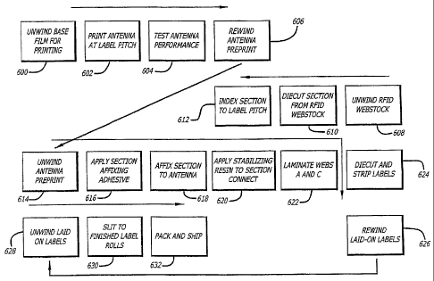
RFID label using such rolls. At step 600, a roll of base film is unwound for
printing. At
step 602 antennas are printed onto the base film at a pitch corresponding to
the pitch
of the labels. At step 604 the performance is tested before the manufacturing
process
proceeds further. At step 606 a roll of preprinted antennas is rewound.
[0080] The cross-web width of the antenna web may be any of a number of
different
widths. In one embodiment, the cross-web width is 16 inches. The pitch of
antennas
and spacing between antennas would depend on the intended label dimensions and
spacing of labels on the final label stock, typically would be in a range from
about 0.5
inch to 32 inches. A typical spacing between adjacent antennas is about .125
inch, but
such spacing can be greater or smaller, if desired.
[0081] In the second phase of the label manufacturing process (which may be
continuous or discontinuous with the first phase), a roll of RFID webstock is
unwound at
step 608. The configuration of small electronic block lCs on the receptor film
may vary
depending on the particulars of the IC placement process (such as FSA), the
requirements of the RFID application (and associated specifications of the
RFID chip
and/or antenna), and other factors. For example, there may be a single row of
small
17
CA 02816180 2013-05-16
WO 03/105063 PCT/US03/01513
electronic block ICs along the web, or there may be multiple rows. For reasons
of
economy, it is typically desirable to put as many ICs on the web as possible
and for this
reason small, densely packed IC's (small electronic blocks) are desirable.
That is, in
one embodiment, the "pitch density" of the small electronic blocks is
maximized. As
previously noted, the "pitch density" is the reciprocal of the product of the
"down web" or
longitudinal pitch and the "cross-web" or lateral pitch.
[0082] Individual sections are cut or separated from the web at step 610. The
cutting
may be accomplished by die cutting or by other cutting methods in the art,
such as laser
cutting, perforating, slitting, punching, or other known means that can scribe
to specific
shapes and sizes. The cut sections are then indexed in such a way as to match
the
pitch of the antennas (which typically is the same as the eventual pitch of
the labels).
The pitch of the labels depends on the size of the labels, which can vary from
application to application. Typically, as discussed previously, the sections
are provided
at a predetermined spacing, and must be "indexed" to match the spacing that is
required for the size of the particular type of label into which the section
will be
incorporated. The indexing may affect the down-web spacing of the sections,
the cross-
web spacing, or both.
[0083] As further background, it should be noted that the pitch density of the
ICs will
generally be greater than the pitch density of the finished label sheets.
Small electronic
block ICs can be packed more closely to one another on their web than the
labels. For
example, it may be possible to have an eight inch wide web of small electronic
block ICs
and a sixteen inch wide sheet of labels, if the pitch of the sections bearing
the small
electronic block ICs is adjusted after the sections are cut from the web to
match the
cross-web pitch of the labels. The only requirement is that there be a one-to-
one
correspondence between the number of lanes of chips, and the number of lanes
of
labels.
[0084] An indexing device can be used to control the relative speed of the web
that
bears the ICs, relative to the speed of the web bearing the antennas, so as to
space
individual IC's appropriately with respect to the antenna web. This
longitudinal (down-
web) indexing device brings the sections into alignment with the antennas, so
that a
section is properly positioned relative to the antenna and can be bonded to
the antenna.
18
CA 02816180 2013-05-16
WO 03/105063 PCT/US03/01513
[00851 Referring now to Fig. 10, the RFID Webstock 502 from the unwind 608 is
tensioned and passed between the cutting die "D" and an anvil "A." The web
passes
through rollers at an in-feed tension isolator 650 and an in-feed drive 652 on
its way to
cutting die "D" and anvil "A." The anvil "A" contains vacuum holding stations
on its
surface that correspond to the layout of antennas on an antenna web. The anvil
includes a hard surface, and is typically of the same diameter as the die so
that as they
rotate together, they are in the same position relative to one another on any
plane on
their surface. The die cuts each individual RFID section out from the matrix
of
surrounding RFID webstock.
[00861 Referring to Fig. 11, vacuum anvil A counter-rotates with "D" and "B"
which
allows the section to be transported from the surface of "D" to a position at
which the
section is joined to an antenna, in this case a nip between rollers "A" and
"B." The
antenna web passes between anvil "A" and base anvil roll "B" which acts as a
lamination member. Roller B has a stepped surface to accommodate the thickness
of
the antenna web such that the diameters of the rollers can be matched to allow
for
rotational registration and tangency of the roller's surfaces with the
sections and
antenna web. Rollers "A" and "B" can form a pressure nip to facilitate the
formation of a
durable bond between electrical connectors of the chip, and the antennas.
Additionally,
heat and/or actinic radiation such as UV radiation (not shown) may be
employed. This
bond may be formed or enhanced using conductive or non-conductive adhesive.
Additionally, these rollers may be used to crimp the two metal surfaces, of
the section
and of the antenna, with or without the use of adhesives. Following formation
of this
bond, the anvil roller "A" completes its rotation to accept the next sections.
[0087] The layout of Fig. 12 would yield a pitch at affixing of approximately
twice the
pitch of the section. Drawn in Fig. 12 is one half of the die face detail.
Therefore, with
each die rotation, four (4) consecutive sections are die cut. Die D is made
with cutting
faces to match the dimensions of the section. Each die section that die cuts
individual
sections has a leading edge L-1 and a trailing edge L-2, such that L-1 cuts
the section
web at the leading edge of the section, and L-2 completes the cut at the
section's
trailing edge.
19
CA 02816180 2013-05-16
WO 03/105063 PCT/US03/01513
[0088] For matching section and antenna pitch with optimal press speeds, it is
necessary to select ratios between the number of cutting sections on die
roller D relative
to both the pitch of the sections and the pitch of the antenna, and to the
relative
diameters of rollers D and A.
[0089] As seen in Figure 10, after passing through the die station 610, the
web passes
through rollers at outfeed drive 654 and at at-feed tension isolator 656, on
its way to
rewind 658.
[0090] Figure 13 illustrates an alternative pressure lamination member B, i.e.
a metal
or polymeric belt, for bonding antennas to sections on anvil roller A'. The
use of a
rotating belt B' provides an extended zone of elevated pressure and/or
temperature to
facilitate adhesive curing, and formation of a durable, metal-to-metal bond
between the
antenna and IC-connector structures. One or more additional set of belt or
roller
combinations (not shown) can be provided to further extend the zone of bond
formation
between the antenna and IC-connector structures. As an option, the RFID
sections
may be placed on an elastomeric band that may be stretched in one or more
dimensions relative to the antenna web to position the RFID sections relative
to the
antennas.
[0091] Referring again to Figure 11, the vacuum anvil A is generally designed
to have
a portion of its rotation with positive vacuum and a second portion without
vacuum. In
addition, a sub-section of the rotational section without vacuum, designated
by P, may
be engineered to operate with positive pressure flow. Each of the three
possible air flow
sections can be engineered to be activated corresponding to the position of
the section
relative to rotation of A.
[0092] As L-2 completes its cutting of the section, vacuum is created at a
surface of
anvil roller A through ports corresponding to the section size. The section is
therefore
held against the surface of roller A as it rotates away from its tangent to
die D. The
matrix from the section web continues in its plane and is rewound as waste.
(Alternatively, the section web can be butt cut, thereby eliminating the
matrix).
(0093] When the RFD section, held on anvil roller A by positive vacuum
approaches
the tangential section with roller B, the vacuum is released, allowing the
section to be
engaged and held by the adhesive previously applied to the antenna web. If
necessary,
CA 02816180 2013-05-16
WO 03/105063 PCMJS03/01513
a positive air flow can be generated to push the section from the surface of A
in section
P; this airflow also may serve to clean the vacuum station. The section then
moves with
the antenna web.
[0094] Concerning down web (or longitudinal) indexing of the sections, the
RFID
webstock transport mechanism can be engineered to direct the web in either the
left-to-
right or right-to-left direction, on commands from an electronic controller.
During the
period commencing when the leading cutting die surface L1 first contacts the
RF1D
webstock, and ending when the trailing cutting die surface L2 ends contact
with the
webstock, the web is transported right-to-left at the same speed as the
antenna web. In
between these cutting cycles, the web transport control provides a controlled-
acceleration left-to-right motion of the web, in order to place the next uncut
section on
the RFID webstock in alignment with the next set of cutting die surfaces Ll,
L2 on die D.
This cycle is then repeated.
[0095] The roller D and its cutting sections can be configured so that there
is a space
between each cutting section that allows the section web to travel in the
opposite
direction from the motion of the die surface without contacting the die
surface. By
matching the space between cutting sections with the elapsed time to cycle the
section
web from one direction to another, the position of each section can be cut at
different
pitches relative to the position of each cutting section. Each cutting section
of D can be
made on the same pitch as the antenna so that as the section web shuttles
between
cutting and non-cutting sections of die D, each section is transported on
anvil roller A at
a matched pitch with the antenna that is moving between rollers A and B. This
allows
for high speed roll-to-roll processing of standardized (and therefore lower
cost) sections,
in a manner that can be adapted to a variety of custom layouts as is typically
found in
labels and tags.
[0096] In one version of the apparatus of Figs. 9-12, the apparatus operates
on an
RFID webstock containing a single lane of chips, and a plurality of such
apparatus is
provided corresponding to the number of lanes of chips on the original RFID
webstock.
These lanes may be slit from the original RED webstock, and optionally may be
spread
apart prior to processing by the vertical indexing apparatus. Alternatively,
the vertical
indexing apparatus may act upon an RFID webstock with multiple lanes of chips.
21
CA 02816180 2015-01-05
WO 03/10063 PC1711S03/01513
10097] The lanes of the web that bears the sections must also be made to match
the
lateral (cross-web) pitch of the lanes of the web bearing the labels and the
antennas.
One way to ensure this "cross-web alignmenr is to use one independent web of
sections for every one independent web of labels and antennae. Another
approach is to
slit the respective webs longitudinally, and then align the slit lanes of
sections to the cut
lanes of labels and antennae. This can be done using a series of spreader
rolls, much
as is done in a conventional slitter assembly. Slitting methods are known and
are
disclosed in a number of U.S. Patents including, for example, U.S. Patent Nos,
3,724,737, 3,989,575, 3,891,157, 4,480,742, and
European Patent Publication EP 0 979 790 A2. The
spreader rolls divert the strands of small electronic block sections to
provide one lane of
sections for every lane of labels.
[0098] Another alternative approach is to cut the small electronic block web
at
maximum pitch density cross-web, and place the resulting lanes on a vacuum
belt that
spreads the lanes. Using apparatus of the type illustrated in U.S. Patent No.
4,480,742,
one may utilize a continuous expanding band or belt to separate the lanes in
the cross-
web direction. Alternatively, a series of laterally spaced belts may undergo
increasing
spacing to separate the lanes in the cross-web direction.
(00991 Concurrent with steps 608-612, the roll of pre-printed antenna is
unwound at
step 614. Adhesive for fixing the sections onto the pre-printed antennas is
applied to
the pre-printed antenna roll at step 616. The sections, which are indexed in
accordance
with the pitch of the labels, are affixed to the antennas at step 618.
[0100] A stabilizing resin may be applied to the bonded sections at step 620.
The
resin of step 620 serves to protect the small electronic block components and
to fix
them into place within the label. Also, the interface between the section and
the
antenna can be fragile. A resinous material may therefore be dispensed over
the
interface area, and then cured to a hard finish that stabilizes the interface
from breaking
from flexure, fatigue or the like. Examples of suitable resinous materials
include silicon
filled thermal curing epoxy or clear filled UV-curable acrylic resin. The
epoxy or acrylic
resin may be dispensed directly onto the interface area, or may be indirectly
dispensed
using a transfer device.
22
CA 02816180 2013-05-16
WO 03/105063 PCT/U503/01513
[0101] At step 622, one or more sheets of facestock are laminated to the web
bearing
The antennas and bonded sections. Referring back to Fig. 4, this step would,
in the
particular embodiment of Fig. 4, serve to adhere the facestock layer 400 to
inlay layer
404. Likewise, additional layers such as face stock layer 412 can be laminated
in
positions above and/or below the inlay layer 404 such as is shown in Figure 5.
[0102] Once the various layers of the label stock have been laminated
together, the
label stock may be die-cut into individual labels at step 624. The labels may
also be cut
into strips or into sheets, as desired. The labels may be rewound onto a take-
up roll at
step 626.
[0103] In the final phase of the manufacturing the die cut labels are unwound
from the
reel at step 628. Through a slitting operation at step 630, the die cut strips
of labels are
sent to individual lines for final processing. After slitting the web into
individual strips, the
strips may be cut into sheets. The sheets may then be packaged and shipped at
step
632.
101041 Fig. 14 is a simplified diagram of a manufacturing process for making
RFID
labels. The base film for printing antenas is unwound at station 600'. The web
bearing
the small electronic blocks is unwound at step 608'. Steps 610' ¨ 620', which
relate to
die cutting and affixing the sections to form an inlay stock, are then
accomplished.
[0105] The inlay stock is laminated with facestock and a bottom web at block
622'.
Labels are die cut and the label matrix is stripped from the laminated web at
block 624'.
The facestock is unwound at reel 636', and the adhesive-coated bottom web and
release liner assembly is unwound at reel 638'. Alternatively unwind 638' may
provide
only a web of release liner to be laminated to adhesive coated directly onto
web 500.
The laid on labels are rewound at area 626'. The label matrix, which is the
extra
material left after the die cutting step, is rewound at station 634'.
[0106] Fig. 16 is a more detailed representation of a manufacturing process as
compared to Fig. 14. Fig. 15 shows a number of different stations that
accomplish
various subprocesses. Considering one subprocess that begins at the left-hand
side of
the drawing, an unwind station 700 carries the RFID webstock described
previously.
The RFID webstock is unwound from station 700 and enters an in-feed station
702 and
then enters a converting module 704. At the converting module 704, the RFID
23
CA 02816180 2013-05-16
WO 03/105063 PCT/US03/01513
webstock is die cut into an array of sections, which are affixed to the pre-
printed
antenna web. The remainder of the webstock (waste matrix) is fed through out
feed
station 706 and ultimately is rewound onto a reel at rewind station 708.
[0107) Another portion of the manufacturing process illustrated in Fig. 15
relates to the
printed antenna web 500, which is provided in a reel at station 710. The pre-
printed
antenna web 500 is unwound from the reel at station 710, then proceeds to an
in-feed
station 712. The preprinted antenna web 500 proceeds to a printing or coating
station
714, at which adhesive is applied to the web. The web 500 continues to station
704
where the array of REID sections are affixed to the pre-printed antennas to
form an
RFD inlay stock 504. The RFID inlay 504 stock proceeds to station 716, at
which the
affixing adhesive is post-cured (e.g. for a B-staged adhesive). Methods for
curing
adhesives are known in the art and, by way of example and not limitation,
include heat
curing, UV, and infrared curing methods.
[0108] An additional stabilizing resin may be applied at a station 718. As
described
previously, the resin may serve to protect the small electronic blocks and to
stabilize the
blocks on the web. A station 720 can serve to inspect the RFID inlay stock,
and
maintain quality control. The RFID inlay stock then continues to an out-feed
station
722, and through station 724. At station 724, a laminating adhesive may be
applied to
the top and bottom sides of the RFID inlay stock. A facestock laminate 506,
which may
be optionally pre-printed or which may be suitable for printing at the user's
facility,
travels through an in-feed station 726 and then to station 724 and station
728. At
station 724 and/or 728, the facestock is laminated to the RFID inlay stock. At
the same
time a bottom layer 508, which may be pre-coated with a pressure sensitive
adhesive
on the bottom, is unwound from a station 730. The bottom layer 508 enters the
stations
724 and 728, where the bottom layer is laminated to the web. The bottom layer
that is
unwound from the reel at station 730 may also include a release liner that
covers the
pressure sensitive adhesive on the bottom of the layer. The facestock layer is
unwound
from reel 731.
[0109] The fully laminated construction then passes through an out-feed unit
732. It is
noted that there are two rewind reels-734 and 736. Rewind reel 734 takes up
the laid-
on labels. Rewind reel 736 takes up the die cut label matrix that is
essentially waste
24
CA 02816180 2013-05-16
WO 03/105063 PCINS03/01513
material from the process in which the labels are cut. The die cutting
operation may be
carried out at station 728. It is noted that the cutting operation is not
limited to die
cutting, but may include other cutting techniques, such as laser cutting,
perforating,
slitting, punching or other methods known in the art.
[0110] Fig. 16 illustrates an alternative arrangement in which stations 750,
752 and
754 serve to print graphics and/or text to the upper facestock after the
facestock
material is unwound from the reel. Three separate print stations 750-754 are
shown to
illustrate that the printing can be done by more than one printhead, such as
in multi-
color printing, if desired. However, it is also possible to print with only
one printhead, as
appropriate. As compared to the arrangement in Fig. 15, this process of Fig.
16
provides for printing onto the upper facestock in the same manufacturing line
as the
other steps in preparing the label stock. It may be desirable to print onto
the facestock
during label fabrication when, for example, variable information such as the
identification information that is stored on a particular chip is to be
printed on the
corresponding label.
[0111] However, it is clear from Fig. 15 that the facestocks may be pre-
printed before
the facestock is wound onto the reel. That is, the pre-printing can be
accomplished off-
site at another facility or at another locatlon besides the manufacturing line
that
accomplishes the various specific steps in making the label. Alternatively,
the facestock
may be partially preprinted offsite, with additional printing done in-line.
[0112] The foregoing has assumed that the IC or small electronic blocks are
provided
on a rolled web that is unwound during the manufacturing process. However, as
an
alternative, the receptor film with microchips may be provided in sheet form
rather than
rolled web form. The sections bearing the individual ICs would then be cut
from pre-cut
sheets, rather than from a roll, and these sections could be integrated into
an RFID tag
or label stock using a pick and place operation. To regulate the pick and
place
operation, the position of a section bearing a small electronic block may be
registered
on a corresponding label by, for example, using a CCD camera to detect a
registration
or alignment mark on or near the label. In lieu of the web-handling equipment
illustrated
above (e.g. for the indexing station, and the attaching station), sheet
handling
equipment may be employed.
CA 02816180 2015-01-05
W0031105063 PC1MS03/41151.3
101131 The pick and place operation may be performed by a pick and place
device,
which may include mechanical and/or vacuum grips to grip a section bearing a
small
electronic block while moving it into the desired location in alignment with
the label. It
will be appreciated that a wide variety of suitable pick and place devices are
well known.
Examples of such devices are the devices disclosed in U.S. Patent Nos.
6,146,901, and
5,564,888, as well as the prior art
devices that are discussed in those patents.
[0114] Alternatively, rotary placers may be utilized to place the sections
upon the
labels. Art example of such a device is disclosed in U.S. Patent No. 5,15,983.
[01151 The integrated circuits or RFD chips may be friction fitted in recesses
in the
RFID microelectronic stock, or they may be secured therein by the use of
adhesives
and/or solder. Electrical connection between the RFD chips and circuitry to be
connected to the antennas may be done with wire bonding, ribbon bonding, tape-
automated bonding, lead frames, flip chip bonding, and/or conductive gluing of
leads.
IV. Material Properties ¨ RFID Webstock and RFID Sections
[01161 It is preferred that the RFID sections be sufficiently rigid so as to
maintain
sufficient dimensional stability and stiffness throughout the processes.
Additional
requirements may be imposed on the substrate material for the RFD
microelectronic
stock by process used to form the stock (e.g. to form reception walls); and to
form
conductive and dielectric materials and assorted electrical interconnect
strictures.
Other desirable properties of the webstock are dictated by the processes for
forming the
inlay stock and for converting the inlay stock to label stock, such as: clean,
sharp die
cutting characteristics; sufficient tensile modulus to avoid undue elongation
under
tension (typically more than 500,000 psi): and adequate strength to avoid web
breaks
during operations such as matrix stripping,
[01171 When the planarization process of Alien Technologies, as discussed
above, is
used, a suitable polymeric film substrate is one that is dimensionally stable
at 150 C for
1 hour, micm-replicable at 260 C, exhibits good adhesion with the planarizing
layer,
exhibits good chemical resistance, the property of laying flat (<0.5" lift for
a 11" sheet),
ready removability from the tool, and die-cuttability.
26
- .
WO 03/105063 PCT/US03/01513
NOT FURNISHED UPON FILING
27
CA 2816180 2018-05-25
CA 02816180 2013-05-16
WO 03/105063 PCT/US03/01513
embossing is significantly less than that of film. When supercalendered Kraft
paper
(SCK) is compared with polysulfone, the tensile modulus is comparable. This
means
that with the same web tension and the same caliper, both SCK and polysulfone
will
stretch to the same extent; however, elongation at break for SCK is much less.
For
paper, moisture sensitivity is a concern, as this would adversely affect the
dimensional
stability of an article according to the present invention. One preferred
alternative is
polycoated paper, such as paper coated with polyethylene or polypropylene on
one or
both sides of the paper. This would reduce any dimensional instability as the
result of
exposure to moisture.
V. Antenna Web
[0124] The antenna portions may be formed on the antenna web using a wide
variety
of materials and processes. For example, one process involves printing on the
antenna
web a conductive material, such as silver conductive ink, in a pattern
defining multiple
antennae. The ink may be printed for example using silk screening techniques,
such as
in a sheet fed or roll operation. The antenna may be printed in a variety of
shapes and
patterns, such as a symmetrical pattern, a non-symmetrical pattern, a bow tie
shaped
pattern, a checkerboard shaped pattern, and/or an unequal shaped pattern, or
other
shapes and patterns known in the art.
[0125] The antennae are typically dried and stored on the web in a roll.
However, as
an alternative, the antennae may be wet printed during the converting process,
and the
sections applied directly to the wet printed ink. When the ink dries, the ink
bonds the
sections to the underlying web. The ink may optionally include a dopant to
increase
adhesion. A layer of pressure sensitive adhesive may be used in conjunction
with the
wet ink for additional stability.
[01261 Suitable methods of forming the antenna include printing conductive
ink,
sputtering metal, laminating foil or hot-stamping, or any method known in the
art for
forming an antenna on a film.
[0127] Considering the sputtered metal approach, it is noted that sputtered
metal
antennas may be made to be very thin while still achieving desired surface
resistance or
conductivity. In one preferred embodiment of a device and method according to
the
present invention, the antenna is formed by metallic sputter coating. Compared
to
28
CA 02816180 2013-05-16
WO 03/105063 PCT/US03/01513
conventional coating of a 60% filled silver ink, comparable surface resistance
can be
achieved by sputtering 1/10 thickness of silver. Additionally, there is no
drying required
as in the case of a silver filled ink coating.
[0128] In one preferred embodiment in which the antenna is formed by metallic
sputter
coating, the sputtering occurs on a 16 in x 6 in square target at a sputter
distance of 4-5
in with a copper or aluminum target at a web speed of up to 1 ft/min and a web
width of
6-10 in. Various alternatives exist for masking. In a first alternative,
masking is applied
on the substrate followed by removal after sputtering. In a second
alternative, a pattern
is masked on the web back coated with PSA which laminates to the substrate
immediately before sputtering, then stripping immediately after sputtering. In
a third
alternative, a permanent mask is used that is very close to the substrate web
(1 cm or
less) so that the divergence of sputter is minimized.
[0129] The precision or definition of the printed elements of lines and spaces
is critical
to the performance of the antenna. With some antenna designs, conventional
printing
may not provide adequate resolution, line/space separation or other quality
characteristics necessary to deliver engineered performance.
[0130] Likewise, control of thickness and smoothness of the printed areas of
an
antenna are criticat to its performance. Variability due to ink formulation,
environmental
conditions, substrate specifications, process conditions and other factors can
impact
both the smoothness and final thickness of printed antennas. Surface tension
effects
underlie many of these variables and place constraints on the amount of ink
that can be
deposited, and how closely graphic elements can be positioned to one another.
[0131] Preferred substrates for the antenna web include, but are not limited
to, high Tg
polycarbonate, poly(ethylene terephthalate), polyarylate, polysulfone, a
norbornene
copolymer, poly phenylsulfone, polyetherimide, polyethylenenaphthalate (PEN),
polyethersulfone (PES), polycarbonate (PC), a phenolic resin, polyester,
polyimide,
polyetherester, polyetheramide, cellulose acetate, aliphatic polyurethanes,
polyacrylonitrile, polytrifluoroethylenes, polyvinylidene fluorides, HDPEs,
poly(methyl -
methacrylates), or a cyclic or acyclic polyolefin. Particularly preferred
substrates include
polysulfone, polyester polyarylate, a norbornene copolymer, high Tg
polycarbonate, and
polyetherimide.
29
CA 02816180 2013-05-16
WO 03/105063 PCT/US03/01513
[0132] It can be desirable to utilize a material that does not unduly stretch
during the
manufacturing process. For example, it may be desirable to utilize a webstock
having a
tensile modulus of more than 500,000 psi.
[0133] Considering now exemplary dimensions, presented by way of example and
not
limitation, in one label embodiment, the section is approximately 7-8 mils
thick, the
antenna coating is about 5¨ 10 microns (0.2 ¨ 0.4 mil). The antenna may be
coated on
a plastic film such as Mylar, having a thickness of approximately 2 ¨ 5 mil.
The
thickness of this particular label embodiment, including a release-coated
backing sheet,
is between approximately 15 ¨20 mils. The purpose of presenting these example
thickness is not to limit the thickness of any of the layers, or of the label
overall. Rather,
it is to illustrate that RF1D labels according to the present invention may be
very thin.
[0134] These various embodiments of labels incorporating IC's are just several
examples of different arrangements that can be imagined for an RFID label or
tag.
Other arrangements are certainly possible, and are within the scope of this
patent
application.
VI. Additional Aspects
[0135] It should be understood that the foregoing Detailed Description
describes
particular embodiments to the present invention for purposes of illustration.
However,
the present invention is not limited to the specific examples that this
Detailed
Description provides. Various changes and modifications may be made to the
labels or
to the manufacturing process within the scope of the invention.
[0136] For example, in embodiments discussed above, sections are cut from a
web,
then applied to another web on which antennae are located. However, it is
possible to,
for example, apply a section to a web, then print or otherwise locate an
antenna onto
the section. This may be done by, for example, printing an antenna on the
section after
the section is applied to a web. Or, alternatively, sputtering metal or
otherwise forming
an antenna onto the section.
[0137] Considering further alternative embodiments, various additional layers
may be
included in the RF1D labels. For instance, there may be additional layers of
cushioning
above or below the IC so as to cushion the component from bumps or shocks
during
normal use. Water-resistant layers such as one or more layers of water-
resistant
CA 02816180 2013-05-16
WO 03/105063 PCT/US03/01513
polymer may be included in the construction. Still other layers can be
included
depending on the particular properties required and the intended application
of the RFID
device.
[0138] Articles according to the present invention can be, for example, a
luggage label
or tag, a laundry label or tag, a label or tag for cataloging library
articles, a label or tag
for identifying an apparel product, a label or tag for identifying a postal
article, a label or
tag for identifying a medical article, or a label or tag for a transportation
ticket. As used
herein, and as recited above, the term "label" refers to an article according
to the
present invention that includes at an adhesive surface for attaching the
article to
another article according to its intended use. The term "tag" refers to an
article
according to the present invention that lacks an adhesive for attachment. A
tag may be
combined in the roll-fed lamination process of the invention with a flat
substrate having
additional functionality, such as fiat material for packaging.
101391 Layers of the label may be bonded together by means other than
adhesive.
For example, the integrated circuit may be held in place with a hot melt resin
or other
substance, which could also serve as a bonding agent. The resin could then
take the
place of an adhesive layer. Layers may also be bonded together by, for
example,
ultrasonic welding.
[0140] The adhesive surface of the label may include adhesive covering the
entire
bottom of the label, or may be coated in a pattern, as is known in the art The
adhesive
may be of the sort that is removable so that the label may be removed from the
substrate after it is applied thereto, or the adhesive may be a permanent type
of
adhesive for permanently bonding the label to the substrate. Alternatively,
the adhesive
may be repositionable, so that the label may be repositioned on the substrate
after it is
initially applied. The adhesive may be water-activated, heat-activated,
pressure-
activated, and/or activated by other means, depending on the specific
application for the
particular label. Alternatively, the label may have no adhesive on the
underside
whatsoever, as to when the label (or tag) is to be attached to the substrate
by other
means, which could include sewing, welding, heat bonding, mechanical fastening
or any
other affixing method known in the tag or label art.
31
CA 02816180 2013-05-16
WO 03/105063 PCT/1JS03/01513
[0141] Another alternative is to provide a label or tag having more than one
RFID chip.
For example, the receptor film may have multiple recesses per section, with
one RFID
chip per recess. The RFID chips may be arranged in a row, column or matrix,
and may
be electrically interconnected with one another.
[0142] As another alternative, a label or tag may include electrical and/or
electronic
components other than RFID chips. For instance, an RFID label or tag may
include a
sensor, a MEMS, or other type of component. The components may be electrically
interconnected to form a circuit. The type of electrical and/or electronic
components to
be used can be selected by one of ordinary skill in the art and depends on the
use of
the label or tag.
[0143] It is again noted that the RFID chip does not necessarily need to be
positioned
in a well as described in Fig. 2, for example. The RFID chip could be atop the
substrate, rather than in a well, or could be otherwise incorporated into or
onto the
substrate. For example, the RFID IC could be a "flip chip" type, wherein the
die is made
so that exposed contacts, or pads on the die have bumps on them. In normal
flip chip
packaging, the die is flipped over and contacted directly into the leads that
provide
electrical contacts for a circuit including the IC. RFID tag and label
constructions using
"flip chip" technology are available for example from KSW Microtec GmbH,
Dresden
Germany.
[0144] As another example of IC packaging technologies compatible with the
present
invention, the manufacturing method of the invention may be used with "lead
frame"
webs. In this embodiment, the IC would be mounted to a web with a conductive
metal
network which may have relatively large area portions, commonly called pads or
flags,
for direct contact with semiconductor chips or dice, and lead elements for
facilitating
electrical interconnection of the chips or dies via intermediate (e.g.,
jumper) connections
to the antenna.
[0145] Consequently, it should be understood that the Detailed Description
does not
describe all of the various changes that might be made to the specific
examples given in
this Detailed Description.
32