Note: Descriptions are shown in the official language in which they were submitted.
CA 02817190 2013-05-07
WO 2012/070693 -1-
PCT/JP2011/077875
DESCRIPTION
TITLE OF THE INVENTION
OPTICAL SENSOR AND IMAGE FORMING APPARATUS
TECHNICAL FIELD
The present invention generally relates to an
optical sensor and an image forming apparatus.
BACKGROUND ART
In an image forming apparatus using an
electrophotographic method such as a digital copier, a laser
printer, and the like, a toner image is transferred onto a
recording medium such as a recording paper and is fixed by
heating and pressurizing at a predetermined condition, thereby
an image is formed on the recording medium such as the
recording paper. In the image forming apparatus, a condition
such as a heat amount, pressure, and the like to fix the toner
image is considered. Especially, in a case of forming an
image at high quality, it is needed to individually set a
condition for fixing the toner image depending on types of the
recording medium.
An image quality for recording to the recording
medium is greatly influenced by material, thickness,
temperature, smoothness, a coating state, and the like. For
CA 02817190 2015-07
WO 2012/070693 -2-
PCT/JP2011/077875
example, regarding the smoothness, a fixing rate of toner is
lower at a concave portion due to an irregularity of the
recording thedium depending on the condition for fixing the
image. As a result, it is not possible to acquire a high
quality image. That is, if the image is not fixed at a
condition corresponding to the smoothness of the recording
medium to which the image is formed, an irregular color or the
like is caused. The high quality image is not acquired.
On the other hand, a concurrent recent development
of the image forming apparatus and diversity of expressing
method, there are more than several hundred types of the
recording papers used as the recording medium. Moreover, a
large variety of names exist depending on grammage, thickness,
or the like for each type of the recording paper. Therefore,
in order to form the high quality image, it is required to set
a fixing condition and the like in detail based on the type,
the name, and the like of the recording paper used as the
recording medium.
Various types of the recording media have been
marketed such as a special paper being embossed on a surface
of a paper as well as a plain paper, a coated paper such as a
gloss coated paper, a matt coated paper, and an art coated
paper, an OHP (Over Head Projector) sheet, and the like. The
types of the recording media are increased. Also, there are
many types of the recording media other than the recording
CA 02817190 2013-05-07
WO 2012/070693 -3- PCT/JP2011/077875
paper and the like.
Currently, settings such as the fixing condition
and the like related to the image forming apparatus are needed'
to be set by a user. Thus, the user is required to have
knowledge related to the various types of the recording media.
Also, if the user needs to set the fixing condition, the user
may feel that it is too complex to perform printing or the
like. Moreover, if there is an error in the fixing condition
set by the user, it is difficult to acquire the high quality
image desired by the user.
Thus, technologies have been inspected, related to
a sensor for identifying the recording medium such as the
recording paper to automatically specify the type of the
recording medium, and an image forming apparatus mounting the
sensor for identifying the recording medium to automatically
specify the type of the recording medium.
For the sensor for identifying the recording medium,
Japanese Laid-open Patent Application No. 2002-340518
discloses a method for detecting friction resistance of a
surface by using a stylus type probe. Japanese Laid-open
Patent Application No. 2003-292170 discloses a method for
detecting stiffness of the recording medium by a pressure
sensor or the like. Also, Japanese Laid-open Patent
Application No. 2005-156380 discloses a method for imaging the
surface of the recording medium by using an image pick up
CA 02817190 2013-05-07
=
WO 2012/070693 -4-
PCT/JP2011/077875
element such as an area sensor or the like, and specifying the
type of the recording medium based on the picked up image, as
a method for identifying the recording medium without contact
with the recording medium.
Also, a method using a reflected light may be
considered as another method for identifying the recording
medium without contact. In the method using the reflected
light, light emitted from a light source such as a light
emitting diode (LED) or the like is emitted to the recording
medium of a target to be identified, and the name or the like
of the recording medium is specified based on a reflected
light amount from the recording medium. The following three =
types of methods are presented, related to the method using
the reflected light.
In a first method, as described in Japanese Laid-
open Patent Application No. H10-160687, the reflected light
amount is detected in a specular reflection direction of light
on a surface of the recording medium, and the name or the like
of the recording medium is specified based on the reflected
light amount in the specular reflection direction.
In a second method, as described in Japanese Laid-
open Patent Application No. 2006-062842, multiple light amount
detectors are provided to detect a amount of light reflected
in the specular reflection direction of light-illuminating the
surface of the recording medium, to also detect a light amount
CA 02817190 2013-05-07
WO 2012/070693 -5-
PCT/JP2011/077875
of a diffuse reflection, and to identify the name or the like
of the recording medium based on the detected light amount in
the specular reflection direction and the light amount in the
diffuse reflection direction.
In a third method, as described in Japanese Laid-
open Patent Application No. H11-249353, light reflected in the
specular reflection direction of light illuminating the
surface of the recording medium is separated by a polarization
beam splitter. Light amount of the separated light is
measured and the name or the like of the recording medium is
deteLmined based on the measured light amount.
However, Japanese Laid-open Patent Applications No.
2002-340518 and No. 2003-292170 disclose a contact method.
Thus, there is a problem in which the surface of the recording
paper or the like as the recording medium may become damaged.
In Japanese Laid-open Patent Application No. 2005-156380, it
is possible to determine the smoothness or the like of the
recording medium but it is difficult to determine the
thickness or the like of the recording medium.
In Japanese Laid-open Patent Applications No. H10-
160687, No. 2006-062842, and No. H11-249353, it is possible to
roughly determine the recording medium, but it is not possible
to determine the thickness or the like of the recording medium
in detail. In an apparatus for determining material of a
sheet member disclosed in Japanese Laid-open Patent
ak 02817190 2013-05-07
WO 2012/070693 -6-
PCT/JP2011/077875
Application No. H10-160687 and apparatuses disclosed in
Japanese Laid-open Patent Applications No. 2006-062842 and No.
H11-249353, it is possible to identify (determine) only a non-
coated paper, a coated paper, and an OHP sheet but it is not
possible to specify the name of the recording medium for a
high quality image formation.
In addition to the above described methods, a
sensor or the like using an ultrasound or the like may be
mounted to identify the recording medium in detail. By
mounting multiple sensors having different schemes, a size of
the image forming apparatus is increased, and also, another
problem is caused such as higher costs of manufacture.
For the sensor for detecting a surface state of a
printing sheet based on the reflected light amount, a
semiconductor laser may be used as a light source to improve
an S/N (Signal to Noise ratio). In this case, a speckle
pattern may occur when a light flux illuminates a rough
surface such as the surface of the printing sheet. Since the
speckle pattern is different depending on portions illuminated
by the light flux, dispersion of detection light at a light
receiving part is caused and accuracy of identifying the
printing paper may be degraded. Accordingly, the LED or the
like has been generally used as the light source.
DISCLOSURE OF THE INVENTION
CA 02817190 2015-01-06
76311-31
-7-
The present invention solves or reduces one or more
of the above problems.
In an aspect of this disclosure, there is provided
an optical sensor, including a light emission system
configured to emit an irradiated light of a linear
polarization in a first polarization direction toward a ,
surface of a target object having a sheet shape from an
incident direction which is inclined with respect to a normal
direction of the surface; a first light detection system
configured to include a first light detector arranged on a
first light path of a specular reflected light, which is.
. emitted from the light emission .system and is specularly
reflected from the target object; and a second light detection
system configured to include a second light detector arranged
on a second light path of a diffuse reflected light which is
diffusely reflected from an incident plane on the target
object, the second light detector receiving second light
passed by an optical element which passes a linear
polarization component of a second polarization direction
perpendicular to the first polarization direction.
CA 02817190 2015-01-06
76311-31
- 7a -
The optical sensor may further comprise at least one third
light detection system configured to include a third light
detector arranged on a third light path of the diffuse
reflected light which is diffusely reflected from the target
object on the incident plane on the target object; and
a processing part configured to specify the target
object based on a ratio of a third output of the third light
detector of the least one third light detection system and the
first output of the first light detection system, and the
second output of the second light detector.
In another aspect of this disclosure, there is
provided an optical sensor, including multiple measurement
systems each configured to include a light emission system
configured to emit first light of a linear polarization in a
first polarization direction to a recording medium; a specular
CA 02817190 2015-01-06
76311-31
- 8 -
reflected light detection system configured to detect specular
reflected light which is specularly reflected from the
recording medium in the first light emitted from the light
emission system; and a diffuse reflected light detection system
configured to include an optical device for passing second
light in a second polarization direction perpendicular to the
first polarization direction, to detect diffuse reflected light
which is diffusely reflected from the recording medium in the
first light emitted from the light emission system. The
optical sensor may further comprise a control part configured
to control light emissions so that timing of a light emission
by a first light emission system is not overlapped with timing
of the light emission by a second light emission system, the
first light emission system and the second emission system
included in the multiple measurement systems.
In a further aspect of this disclosure, there is
provided an optical sensor, including multiple light emission
systems each configured to emit first light of a linear
polarization in a first polarization direction to a recording
medium; multiple specular reflected light detection systems
each configured to detect specular reflected light which is
specularly reflected from the recording medium in the first
light emitted from a respective light emission system in the
multiple light emission systems; and a diffuse reflected light
detection system configured to include an optical device for
passing second light in a second polarization direction
perpendicular to the first polarization direction, to detect
diffuse reflected light which is diffusely reflected from the
recording medium in the first light emitted from the respective
light emission system. The optical sensor may further comprise
CA 02817190 2015-01-06
76311-31
- 8a -
a control part configured to control light emissions so that
timing of a light emission by a first light emission system is
not overlapped with timing of the light emission by a second
light emission system, the first light emission system and the
second emission system included in the multiple measurement
systems.
ak 02817190 2013-05-07
WO 2012/070693 -9-
PCT/JP2011/077875
BRIEF DESCRIPTION OF THE DRAWINGS
Other objects, features, and advantages of the
present invention will become more apparent from the following
detailed description when read in conjunction with the
accompanying drawings, in which:
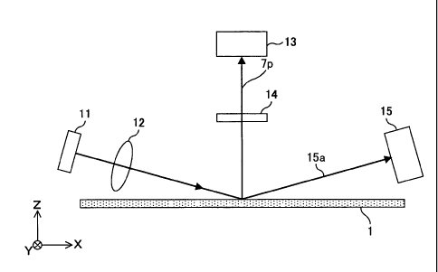
FIG. 1A, FIG. 1B, and FIG. 1C are diagrams for
explaining reflected light from a recording paper.
FIG. 2 is a diagram illustrating a =correlation
between a light amount of an internal diffuse reflection and
thickness of the recording paper.
FIG. 3 is a diagram illustrating a correlation
between the light amount of the internal diffuse reflection
and a density of the recording paper.
FIG. 4A and FIG. 4B are diagrams for explaining the
reflected light in a case of emitting light along a grain of
the recording paper.
FIG. 5A and FIG. 5B are diagrams for explaining the
reflected light in a case of emitting the light
perpendicularly to the grain of the recording paper (part 1).
FIG. 6A and FIG. 6B are diagrams for explaining the
reflected light in the case of emitting the light
perpendicularly to the grain of the recording paper (part 2).
FIG. 7 is a diagram for explaining an influence of
a number of light emitting elements, which affects a contrast
CA 02817190 2013-05-07
WO 2012/070693 -10-
PCT/JP2011/077875
ratio of a speckle pattern.
FIG. 8 is a diagram illustrating a relationship
between the contrast ratio of the speckle pattern and a total
light amount in a case of changing the number of light
emitting elements and in a case of changing the light amount
for each of the light emitting elements.
FIG. 9 is a diagram for explaining light intensity
distribution of the speckle pattern in a case of changing a
driving current of a light source.
FIG. 10 is a diagram for explaining an effective
light intensity distribution of the speckle pattern in a case
of changing the driving current of the light source at high
speed.
FIG. 11 is a top view of an optical sensor in a
first embodiment.
FIG. 12 is a lateral view of the optical sensor in
the first embodiment.
FIG. 13 is a diagram illustrating a configuration
of a surface emitting laser array.
FIG. 14 is a diagram for explaining a method for
controlling the optical sensor in the first embodiment.
FIG. 15 is a diagram illustrating a relationship a
type of the recording medium and outputs of the specular
reflected light detection system and the diffuse reflected
light detection system (part 1).
CA 02817190 2013-05-07
WO 2012/070693 -11--
PCT/JP2011/077875
FIG. 16 is a diagram illustrating the relationship
a type of the recording medium and the outputs of the specular
reflected light detection system and the diffuse reflected
light detection system (part 2).
FIG. 17 is a top view of the optical sensor in a
second embodiment.
FIG. 18 is a lateral view of the optical sensor in
the second embodiment.
FIG. 19 is a top view of the optical sensor in a
third embodiment.
FIG. 20 is a top view of the optical sensor in a
fourth embodiment.
FIG. 21 is a top view of the optical sensor in a
fifth embodiment.
FIG. 22 is a lateral view of the optical sensor in
the fifth embodiment.
FIG. 23 is a top view of the optical sensor in a
sixth embodiment.
FIG. 24 is a lateral view of the optical sensor in
the sixth embodiment.
FIG. 25 is a diagram illustrating a configuration
of a color printer in a seventh embodiment.
FIG. 26 is a diagram for explaining a surface
emitting laser array in which light emitting elements are not
equally spaced.
CA 02817190 2015-07
WO 2012/070693 -12-
PCT/JP2011/077875
FIG. 27 is a diagram for explaining a light
intensity distribution of the speckle pattern in a case in
which the light emitting elements are equally spaced.
FIG. 28 is a diagram for explaining a light
intensity distribution of the speckle pattern in a case in
which the light emitting elements are not equally spaced.
FIG. 29A, FIG. 29B, and FIG. 29C are diagrams for
explaining a change of a detected light amount due to a
displacement between a measurement plane and a surface of the
recording medium.
FIG. 30 is a diagram for briefly explaining a
configuration of a color printer according to an eighth
embodiment.
FIG. 31 is a diagram for explaining a configuration
of an optical sensor in FIG. 30 in the eighth embodiment.
FIG. 32 is a diagram for explaining a surface
emitting laser array in the eighth embodiment.
FIG. 33 is a diagram for explaining an incident
angle of an incident light to a recording paper in the eighth
embodiment.
FIG. 34 is a diagram for explaining an arrangement
location of two light receivers in the eighth embodiment.
FIG. 35A is a diagram for explaining a surface
specular reflected light in the eighth embodiment, FIG. 35B is
a diagram for explaining a surface diffuse reflected light in
CA 02817190 2013-05-07
WO 2012/070693 -13-
PCT/JP2011/077875
the eighth embodiment, and FIG. 35C is a diagram for
explaining an internal diffuse reflected light in the eighth
embodiment.
FIG. 36 is a diagram for explaining light
respectively received by light receivers in the eighth
embodiment.
FIG. 37 is a diagram for explaining a relationship
between signal levels S1 and S2 and a name of the recording
paper in the eighth embodiment.
FIG. 38 is a diagram for explaining influence of
the number of light emitting elements which affect a contrast
ratio of the speckle pattern in the eighth embodiment.
FIG. 39 is a diagram for explaining a relationship
between the contrast ratio of the speckle pattern and a total
light amount in a case in which the number of the light
emitting elements is changed and in a case in which the light
amount for each of the light emitting elements is changed in
the eighth embodiment.
FIG. 40 is a diagram for explaining a light
intensity distribution of the speckle pattern when a driving
current of the light source is changed in the eighth
embodiment.
FIG. 41 is a diagram for explaining an effective
light intensity distribution of the speckle pattern when the
diving current of the light source is changed at higher speed
CA 02817190 2013-05-07
WO 2012/070693 -14-
PCT/JP2011/077875
in the eighth embodiment.
FIG. 42 is a diagram for explaining another
configuration of the optical sensor in the eighth embodiment.
FIG. 43 is a diagram for explaining the surface
emitting laser array in which light emitting elements are
unequally spaced in the eighth embodiment.
FIG. 44 is a diagram for explaining the light
intensity distribution of the speckle pattern in which the
light emitting elements are unequally spaced in the eighth
embodiment.
FIG. 45 is a diagram for explaining the light
intensity distribution of the speckle pattern in which the
light emitting elements are not equally space in the eighth
embodiment.
FIG. 46 is a diagram for explaining a first
variation of the optical sensor in the eighth embodiment (part
1).
FIG. 47 is a diagram for explaining the first
variation of the optical sensor in the eighth embodiment (part
2).
FIG. 48 is a diagram for explaining a second
variation of the optical sensor in the eighth embodiment (part
1).
= FIG. 49 is a diagram for explaining the second
variation of the optical sensor in the eighth embodiment (part
CA 02817190 2013-05-07
WO 2012/070693 -15-
PCT/JP2011/077875
2).
FIG. 50 is a diagram for explaining a third
variation of the optical sensor in the eighth embodiment (part
1).
FIG. 51 is a diagram for explaining the third
variation of the optical sensor in the eighth embodiment (part
2).
FIG. 52 is a diagram for explaining a relationship
between a combination of a signal level S4 or S1 and a signal
level S3 or S2, and the name of the recording paper in the
eighth embodiment.
FIG. 53A and FIG. 53B are diagrams for explaining
influence of disturbing light in the eighth embodiment.
FIG. 54 is a diagram for explaining a fourth
variation of the optical sensor in the eighth embodiment.
FIG. 55 is a diagram for explaining a fifth
variation of the optical sensor in the eighth embodiment.
FIG. 56A through FIG. 56C are diagrams for
explaining a change of a detected light amount due to a
displacement between a measurement plane and the surface of
the recording paper in the eighth embodiment.
FIG. 57 is a diagram for explaining a relationship
between thickness and the signal level S1 in the eighth
embodiment.
FIG. 58 is a diagram for explaining a relationship
CA 02817190 2013-05-07
WO 2012/070693 -16--
PCT/JP2011/077875
between a density and the signal level S1 in the eighth
embodiment.
BEST MODE FOR CARRYING OUT THE INVENTION
In the following, an embodiment of the present
invention will be described with reference to the accompanying
drawings. The same component parts and the like are indicated
by the same reference numerals and the explanation thereof
will be omitted.
[First Embodiment]
(Classification of Reflected Light)
First, reflected light in a case of emitting light
onto a recording medium such as a recording paper or the like
will be described with reference to FIG. 1A, FIG. 1B, and FIG.
1C. In the case of emitting the light onto a recording paper
1 as the recording medium, it is possible to separate
reflected light into light reflected from a surface of the
recording paper 1 and light reflected inside the recording
medium. Moreover, it is possible to separate the light
reflected from the surface of the recording paper 1 into
specular reflected light and diffuse reflected light. In the
first embodiment, light specularly reflected from the surface
of the recording paper 1 illustrated in FIG. LA is described
as a surface specular reflected light. Light diffusely
reflected from the surface of the recording paper 1 is
CA 02817190 2013-05-07
WO 2012/070693 -17- PCT/JP2011/077875
illustrated in FIG. 1B. In the first embodiment, a case of
the recording medium being the recording paper 1 to which the
light is illuminated will be described. Alternatively, the
recording medium may be a resin film, a fabric, a skin, and
the like. A similar measurement and the like may be performed.
The surface of the recording paper 1 as the
recording medium is formed by flat portions and slope portions.
Smoothness of the recording paper 1 is determined by a ratio
of the flat portions and the slope portions. Light reflected
on the flat portions becomes the surface specular reflected
light, and light reflected on the slopes becomes the surface
diffuse reflected light. The greater the smoothness of the
recording medium increases a light amount of the surface
specular reflected light.
On the other hand, in a case in which the recording
medium is the recording paper 1, light reflected inside the
recording paper 1 includes the diffuse reflected light alone
due to a multiple reflection caused by fabric formed by the
recording paper 1. The light diffusely reflected inside the
recording paper 1 illustrated in FIG. 10 is described as
internal diffuse reflected light.
As illustrated, light reflected from the recording
paper 1 as the recording medium includes the surface specular
reflected light, the surface diffuse reflected light, and the
internal diffuse reflected light. In the light, a
CA 02817190 2013-05-07
WO 2012/070693 -18- PCT/JP2011/077875
polarization direction of light reflected on the surface of
the recording paper 1 is not rotated. That is, the
polarization directions of the surface specular reflected
light and the surface diffuse reflected light are not changed.
In order to rotate the polarization direction of emitted light,
the light is needed to be reflected at a slope surface in a
rotation direction with respect to a light axis. Accordingly,
in a case in which a light source at which the light is
emitted, an area illuminated by the light, and a photodetector
exist on the same plane, the reflected light in which the
polarization direction is rotated is not reflected to a
direction in which the photodetector exists. Thus, the
photodetector may not detect the reflected light. On the
contrary, the internal diffuse reflected light is regarded as
light multiplication reflected due to the fabric inside the
recording paper 1. Thus, the polarization direction is
rotated with respect to light emitted from the light source.
As described above, an optical device for
separating lights having different polarization directions is
provided in front of the photodetector. The optical device
may be a polarizing filter. Thus, it is possible to detect
light having a polarization component in a perpendicular
direction to a component of a linear polarization emitted from
the light source. It is possible to separate and detect the
internal diffuse reflected light alone. Based on a detected
CA 02817190 2015-07
WO 2012/070693 -19-
PCT/JP2011/077875
light amount of the internal diffuse reflected light, it is
possible to determine a type and thickness of the recording
paper 1 as the recording medium.
In detail, as illustrated in FIG. 2, there is a
correlation between the light amount of an internal diffuse
reflection and the thickness of the recording paper 1. The
thicker the recording paper 1, the increased the light amount
of an internal diffuse reflection. Accordingly, it is
possible to determine the thickness of the recording paper 1
based on the light amount of the internal diffuse reflection.
Moreover, as illustrated in FIG. 3, there is the correlation
between the light amount of the internal diffuse reflection
and density of the recording paper 1. The higher the density
of the recording paper 1, the increased the light amount of
the internal diffuse reflection. Accordingly, it is possible
to determine the density of the recording paper 1 based on the
light amount of the internal diffuse reflection. FIG. 2
illustrates a measurement result in a case of multiple
different thicknesses of the recording paper 1. FIG. 3
illustrates another measurement result in a case of multiple
different densities of the recording paper 1.
(Grain of Recording Paper)
The recording paper 1 as the recording medium is
produced so as to be conveyed in one direction in a production
stage. A orientation of the fabric forming the recording
CA 02817190 2015-07
WO 2012/070693 -20- PCT/JP2011/077875
paper 1, called a grain, is caused on the recording paper 1.
The orientation of the fabric is formed along a direction of
conveyance of the recording paper 1 in the production stage.
Therefore, based on a direction of emitting the light, it is
possible to acquire different reflection features even in a
case of the same recording paper 1, and to determine the name
or the like of the recording paper 1 based on the different
reflection features. That is, it is possible to determine the
name of the recording paper 1 based on a difference of the
grain.
A determination of the recording paper 1 will be
described with reference to FIG. 4A and FIG. 43, and FIG. 5A
and FIG. 5B. In FIG. 4A and FIG. 4B, and FIG. 5A and FIG. 53,
it is assumed that an orientation of concavity and convexity
due to the grain is 100 % for the recording paper 1. The
grain is formed according to a Y axis direction. As
illustrated in FIG. 4A and FIG. 4B, in a case of emitting
light 11 in a direction along the grain of the recording paper
1, that is, in a case in which the grain of the recording
paper 1 and a light path of the light 11 are on the same plane,
in other words, in a case in which the light path of the light
11 exits on a plane parallel to a YZ plane, a surface of the
recording paper 1 may be regarded as a flat and smooth plane,
= and the surface diffuse reflected light may hardly occurr.
Also, as the diffuse reflected light, an internal diffuse
ak 02817190 2013-05-07
WO 2012/070693 -21- =
PCT/JP2011/077875
reflected light 11b, which is diffusely reflected inside the
recording paper 1, occurs. Accordingly, in this case,
reflected light of the light 11 is almost a surface specular
reflected light lla. FIG. 4A is a perspective diagram
illustrating a state in which reflected light of the light 11
illuminating the recording paper 1 is almost the surface
specular reflected light lla. FIG. 4B is a cross-sectional
diagram illustrating a surface along the grain of the
recording paper 1. That is, in FIG. 4B, a cross-sectional
surface in the YZ plane is illustrated.
Next, as illustrated in FIG. 5A and FIG. 5B, in a
case of emitting light 12 in a perpendicular direction to the
grain of the recording paper 1, that is, in a case in which
the light path of the light 12 illuminated on the recording
paper 1, an illuminated surface may be regarded as a slope
portion on an irregular surface of the recording paper 1.
Thus, the light 12 is diffusely reflected from the surface and
the specular reflection hardly occurs. Thus, the light amount
of a surface diffuse reflected light 12a is increased. In
this case, also, as the diffuse reflected light, the internal
diffuse reflected light 12b, which is diffusely reflected
inside the recording paper 1, occurrs but the light amount is
less. Thus, the reflected light of the light 12 is almost the
surface diffuse reflected light 12a. FIG. 5A is a perspective
diagram illustrating a state in which the reflected light of
CA 02817190 2015-07
WO 2012/070693 -22-
PCT/JP2011/077875
the light 12 illuminating the recording paper is mostly the
surface diffuse reflected light 12a. FIG. 5B is a cross-
sectional diagram illustrating a surface perpendicular to the
grain of the recording paper 1. That is, in FIG. 5B, a cross-
sectional surface in an XZ plane is illustrated.
Moreover, in a case of emitting light in the
perpendicular direction to the grain of the recording paper 1,
the light amounts of the surface diffusion reflected light and
the internal diffuse reflected light, which are detected, are
varied depending on an incident direction of the light toward
the recording paper 1. In detail, as illustrated in FIG. 6A
and FIG. 6B, by emitting light 13 and light 14 which are
opposite to each other in the perpendicular direction to the
grain of the recording paper 1, the light amounts of the
surface diffuse reflected light and the internal diffuse
reflected light are varied. Variations of the light amounts
are caused by different slopes at both ends of the grain of
the recording paper 1. The different slopes at both ends of
the grain of the recording paper 1 have been investigated.
That is, even in a case of similarly emitting light
at approximately the same angle with respect to the recording
paper 1 in the perpendicular direction to the grain of the
recording paper 1, if the incident direction of the light
illuminating the recording paper ,1 is changed, an incident
angle becomes different due to the slope on the irregular
CA 02817190 2013-05-07
WO 2012/070693 -23-
PCT/JP2011/077875
surface of the recording paper 1. In detail, light 13 emitted
to the recording paper 1 enters at an angle near a vertical
angle with respect to the slope of the recording paper 1.
Thus, the light entering inside the recording paper 1 is
increased, a surface diffuse reflected light 13a is increased,
and an internal diffuse reflected light 13b is increased.
Also, since light 14 enters the recording paper 1 at an angle
sharper than an angle of the light 13 with respect to the
slope of the recording paper 1, light entering inside the
recording paper 1 is decreased. Thus, a surface diffuse
reflected light 14a is increase and a internal diffuse
reflected light 14b is increased. This state occurs in a case
in which the light enters perpendicularly to the grain of the
recording paper 1. In a case of emitting the light along the
grain of the recording paper 1, even if the incident direction
of the light is changed, a ratio or the like of the surface
specular reflected light and the internal diffuse reflected
light may not be varied.
As described above, summarizing a relationship
between the incident direction of the light entering the
recording paper 1 and the reflected light, the ratio between
the surface specular reflected light and the surface diffuse
reflected light in light emitted along the grain of the
recording paper 1 is different from that in light emitted
perpendicularly to the grain of the recording paper 1.
CA 02817190 2013-05-07
WO 2012/070693 -24-
PCT/JP2011/077875
Moreover, in a case in which the incident direction of the
light entering the recording paper 1 is an opposite direction,
that is, in a Case in which an angle of the incident direction
of entering light is 1800, as long as the light enters along
the grain of the recording paper 1, a different incident
direction of the entering light may not influence the light
amounts of the surface specular reflected light and the
internal diffuse reflected light. However, in a case in that
the light enters perpendicularly to the grain of the recording
paper 1, when the incident direction of the light is changed,
the light amounts of the surface specular reflected light and
the internal diffuse reflected light are varied.
In the above explanation, it is assumed that the
orientation of the grain of the recording paper 1 is 100 %.
On an actual recording paper, the grain is formed. A degree
and the like of the orientation of the grain are different
depending on the production stage, a production condition, and
the like. Based on characteristics of the actual recording
paper, the reflected light of the light entering the recording
paper 1 is classified into the surface specular reflected
light, the surface diffuse reflected light, and the internal
diffuse reflected light, and respective light amounts are
measured. By this manner, it is possible to determine the
name and the type of the recording paper 1 in detail, and to
improve accuracy of determining the recording paper 1.
CA 02817190 2013-05-07
WO 2012/070693 -25- PCT/JP2011/077875
(Detection Accuracy of Internal Diffuse Reflected Light)
A high accurate detection method of the internal
diffuse reflected light will be described. In order to detect
the internal diffuse reflected light at higher accuracy, first,
it is required to exclude a component of the surface specular
reflected light in a detection direction at least. However,
it is difficult to completely exclude light other than light
of the linear polarization in one direction alone in an actual
irradiation system. That is, it is difficult to leave light
of the linear polarization in a first polarization direction
alone. The reflected light on the surface of the recording
paper 1 includes a component in a second polarization
direction perpendicular to the first polarization direction.
In detail, in a case in which a photodetector is
arranged at a location where the surface specular reflected
light is detected and the light amount of the component of the
light in the second polarization direction by using an optical
filter, if the component of the light in the second
polarization direction is included in the light emitted on the
recording paper 1, this component is also detected by the
photodetector. Thus, the light amount of the internal diffuse
reflected light may not be precisely detected. In this case,
since the light amount of the internal diffuse reflected light
is generally smaller, the light amount of the component of the
light in the second poralization direction included in the
CA 02817190 2015-07
WO 2012/070693 -26-
PCT/JP2011/077875
light emitted onto the recording paper 1 may be greater than
that of the internal diffuse reflected light. Also, it may be
possible to make the light emitted onto the recording paper 1
be a perfect light in the first polarization direction. In
this case, it is required to use a polarization filter having
a higher extinction ratio. Thus, this configuration costs
more.
Next, when the internal diffuse reflected light is
detected, it is required to perform the detection in a
direction approximately perpendicular with respect to the
surface of the recording paper 1. Since the internal diffuse
reflected light may be regarded as perfectly diffuse reflected
light, the light amount of reflection with respect to the
detection direction may be approximated to a Lambert
distribution. The reflected light amount becomes the greatest
in the direction perpendicular to the surface of the recording
paper 1. The light amount of the internal diffuse reflected
light is a slight amount. In view of improving a S/N, by
providing the photodetector to be a light receiving part in
the direction perpendicular to the surface of the recording
paper 1, it is possible to improve the accuracy. In a case of
arranging a light source emitting light to the recording paper
1 in which a radiation direction of the light is changed, and
multiple photodetectors, it is required to arrange the
multiple photodetectors in the direction perpendicular to the
CA 02817190 2015-07
WO 2012/070693 =-27- PCT/JP2011/077875
surface of the recording paper 1. It is preferable to arrange
the multiple photodetectors in an approximately perpendicular
direction so that the multiple photodetectors do not interfere
with each other. Also, a beam splitter may be provided to
divide the light, or a polarization filter capable of being
driven may be provided to reduce the interference.
(Suppression Method of Speckle Nozzle)
As described above, in view of the reflected light
amount, it is preferable to user a semiconductor laser as the
light source. However, in a case of using the semiconductor
laser as the light source of an optical sensor for detecting a
surface state of the recording paper 1, since coherent light
emitted from the light source is diffusely reflected at points
on a rough surface such as the surface of the recording paper
1 and reflected lights at the points interfere with each other,
a speckle pattern occurs. In the speckle pattern, the
reflected lights interfere with each other in a reflection
direction, and noises are caused in an output of each of the
photodetectors. Thus, the S/N is degraded. In the first
embodiment, a speckle noise is described as the degraded S/N,
a measure for this problem will be described in the following.
Inventors investigated a relationship between a
number of the light emitting elements and a contrast ratio of
the speckle pattern by using a Vertical-Cavity Surface-
Emitting Laser (VCSEL) as the light source in which multiple
CA 02817190 2013-05-07
WO 2012/070693 -28-
PCT/JP2011/077875
light emitting elements are arranged in two dimensions. An
investigation result is illustrated in FIG. 7. In the first
embodiment, the contrast ratio of the speckle pattern is
defined as a value in which a difference between a maximum
value and a minimum value in observation intensity is
normalized.
Observation of the speckle pattern is performed by
using a beam profiler, regarding a Y-axis direction (diffuse
direction). The contrast ratio of the speckle pattern is
calculated based on an observation result acquired by the beam
profiler. As samples for =observation targets, three types of
plain papers (a plain paper A, a plain paper B, and a plain
paper B) having different smoothness degrees and a glossy
paper is used. The plain paper A is a paper in which an Oken
type smoothness indicates 33 sec. The plain paper B is a
paper in which the Oken type smoothness indicates 50 sec. The
plain paper C is a paper in which the Oken type smoothness
indicates 100 sec.
As illustrated in FIG. 7, when the number of the
light emitting elements is increased, the contrast ratio of
the speckle pattern tends to decrease. Also, this tendency
does not depend on the type of a paper.
Moreover, the inventors performed an
experimentation to confirm that an effect of decreasing the
contrast ratio of the speckle pattern originated in an
¨
CA 02817190 2015-07
WO 2012/070693 -29-
PCT/JP2011/077875
increase of the number of the light emitting elements but did
not originated in an increase of a total light amount. An
experimentation result is illustrated in FIG. 8.
FIG. 8 illustrates a change of the contrast ratio
with respect to the total light amounts in a case of changing
the number of the light emitting elements while each light
amount of the light emitting elements is fixed (for example,
1.66 mW) and in a case of changing the light amount for each
of the light emitting elements while the number of the light
emitting elements is fixed to 30 elements.
In the case of changing the light amount for each
of the light emitting elements while the number of the light
emitting elements is fixed, the contrast ratio is
approximately constant. On the contrary, in the case of
changing the number of the light emitting elements while each
light amount of the light emitting elements is fixed, if the
light amount is less, that is, the number of the light
emitting elements is small, the contrast ratio is high. When
the number of the light emitting elements is increased, the
contrast ratio gradually decreases. Accordingly, it has
confirmed that the effect of decreasing the contrast ratio in
the speckle pattern depends on the increase of the number of
the light emitting elements, but does not depend on the
increase of the light amount.
Also, the inventors investigated whether it is
ak 02817190 2013-05-07
WO 2012/070693 -30-
PCT/JP2011/077875
possible to suppress the speckle pattern by varying a
wavelength of the light emitted from the light source.
In the surface emitting laser (VCSEL), it is
possible to control the wavelength of the light emitted by a
driving current. When the driving current is changed, heat is
generated in the VCSEL, and a refraction index is varied.
Then, an effective resonator length is changed.
FIG. 9 illustrates light intensity distribution
acquired by observing the speckle pattern by the beam profiler
in a case in which the VCSE is applied as the light source and
an emitted light amount is changed from 1.4 mW to 1.6 mW by
changing the driving current. As illustrated in FIG. 9,
depending on the change of the driving current, the wavelength
of the light emitted from the light source is changed. Thus,
it is confirmed that the light intensity distribution is
changed.
FIG. 10 illustrates an effective light intensity
distribution in a case of changing the driving current at high
speed. The light intensity distribution is the same as an
average value of the light intensity distribution in multiple
driving currents illustrated in FIG. 9. Thus, it is confirmed
that a change of the light intensity is suppressed. The
contrast ratio of the speckle pattern in the case of changing
the driving current indicates 0.72, and the contrast ratio of
the speckle= pattern in the case of fixing the driving current
CA 02817190 2013-05-07
WO 2012/070693 -31-
PCT/JP2011/077875
indicates 0.96. Thus, the contrast ratio in the former case
is suppressed to be lower than that in the latter case.
Accordingly, in a case of driving the surface
emitting laser (VCSEL), for example, flow of the driving
current may be controlled so as that a current value forms a
triangular waveform in a temporal response. Therefore, it is
possible to suppress the contrast ratio to be lower.
(Optical Sensor)
Next, an optical sensor in the first embodiment
will be described. In the first embodiment, light
illuminating on the recording paper 1 is regarded as linear
polarized light and an S-wave, and a reflected light amount is
described as a SP intensity in a case in which the .
photodetector arranged in an approximately perpendicular
direction to the surface of the recording paper detects a P-
wave. The .reflected light amount indicates the light amount
of the internal diffuse reflected light. Similarly, the light
illuminating the recording paper 1 is regarded as light of the
linear polarized light and the P-wave, and the reflected light
amount is described as a PS intensity in a case in which the
photodetector arranged in the approximately perpendicular
direction to the surface of the recording paper 1 detects the
S-wave.
Also, the light illuminating the recording paper 1
is regarded as the linear polarized light and the S-wave. The
ak 02817190 2013-05-07
WO 2012/070693 -32- PCT/JP2011/077875
polarizing filter is not provided for the photodetector for
detecting light specularly reflected on the surface of the
recording paper 1, that is, the photodetector for detecting
light reflected at =an approximately the same angle as an
incident angle of the light illuminating the recording paper 1.
Thus, the photodetector detects light including components of
both S-wave and P-wave. The reflected light amount detected
by the photodetector is described as a SN intensity. An
incident angle e or the like of the light illuminating the
recording paper 1, that is, incident light entering the
recording paper 1 indicates an angle with respect to a normal
line of the surface of the recording paper 1. An angle for
arranging the photodetector may be denoted by an angle 0, 0,
or the like with respect to the surface of the recording paper
1 in which a location for the light to enter the recording
paper 1 is set as a reference. In the first embodiment, a
case, in which the light illuminating the recording paper 1 is
the S-wave, is described. However, the first embodiment is
not limited to this case but the light illuminating the
recording paper 1 may be the P-wave.
Next, an optical sensor 1001 in the first
embodiment will be described with reference to FIG. 11 and FIG.
12. The optical sensor 1001 includes two measurement systems:
a first measurement system 110 and a second measurement system
120. The first measurement system 110 includes a first light
ak 02817190 2013-05-07
WO 2012/070693 -33-
PCT/JP2011/077875
emission system 111, a first specular reflected light
detection system 112, and a first diffuse reflected light
detection system 113. Also, the second measurement system 120
includes a second light emission system 121, a second specular
reflected light detection system 122, and a second diffuse
reflected light detection system 123.
The first measurement system 110 and the second
measurement system 120 are covered with a dark box 180. An
opening part 181 is provided to the dark box 180 to illuminate
light onto the surface of a recording paper 100. The first
measurement system 110 and the second measurement system 120
are enclosed by the dark box 180 and the recording paper 100.
External light and the like do not entered from the outside.
Thus, it is possible to perform a precise measurement. Also,
the first light emission system 111, the first specular
reflected light detection system 112, the first diffuse
reflected light detection system 113, the second light
emission system 121, the second specular reflected light
detection system 122, and the second diffuse reflected light
detection system 123 are connected to a control part 190.
Also, in the first embodiment, the first
measurement system 110 and the second measurement system 120
are arranged so that an angle, which is formed by a light path
of light emitted from the first light emission system 111 and
another light path of light emitted from the second light
CA 02817190 2013-05-07
WO 2012/070693 -34-
PCT/JP2011/077875
emission system 121, becomes 1500 on a XY plane. That is, an
angle, which is formed by a component parallel to the
recording paper 100 in the light emitted from the first light
emission system 111 and another component parallel to the
recording paper 100 in the light emitted from the second light
emission system 121, becomes 150 on the XY plane. It is
preferable for this angle to be more than 90 and less than
180 . In a case in which the angle is more than 90 and less
than 180 , the light emitted from the second light emission
system 121 includes a component emitted from an opposite
direction as illustrated in FIG. 6 =with respect to the light
emitted from the first light emission system 111. Therefore,
it is possible= to identify the recording medium at higher
accuracy. Also, in the first embodiment, "emitting light on
the XY plane" indicates a state of projection on the XY plane.
= The first light emission system 111 includes a
light source 114, a collimating lens 115, and the like. A
configuration of the second light emission system 121 is the
same as the configuration of the first light emission system
= 20 111. The first light =emission system 111 is arranged at a
location where the light enters at an angle el with respect to
the normal line of the recording paper 100. The second light
emission system 121 is arranged at a location where the light
enters at an angle 02 with respect to the normal line of the
recording paper 100. In the first embodiment, the angle Al
CA 02817190 2013-05-07
WO 2012/070693 -35-
PCT/JP2011/077875
and the angle 02 are the same and approximately 800. The
angle 01 is regarded as an angle formed by a direction of the
light emitted from the first light emission system 111 to the
recording paper 100 and the normal line of the surface of the
recording paper 100. The angle 02 is regarded as an angle
formed by a direction of the light emitted from the second
light emission system 121 to the recording paper 100 and the
normal line of the surface of the recording paper 100.
The first specular reflected light detection system
112 is used to detect the surface specular reflected light in
the light emitted from the first light emission system 111 to
the recording paper 100, and includes a photodetector 116
formed by a light receiving element such as a photo diode or
the like. The second specular reflected light detection
system 122 is used to detect the surface specular reflected
light in the light emitted from the second light emission
system 121 to the recording paper 100, and includes a
photodetector 126 foLmed by a light receiving element such as
a photo diode or the like.
The first diffuse reflected light detection system
113 is used to detect the surface diffuse reflected light and
the internal diffuse reflected light in the light emitted from
the first light emission system 111 to the recording paper 100,
and includes a photodetector 117 formed by a light receiving
element such as a photo diode or the like. A polarizing
ak 02817190 2013-05-07
WO 2012/070693 -36-
PCT/JP2011/077875
filter 118 is provided in front of the photodetector 117. The
second diffuse reflected light detection system 123 is used to
detect the surface diffuse reflected light and the internal
diffuse reflected light in the light emitted from the second
light emission system 121 to the recording paper 100, and
includes a photodetector 127 formed by a light receiving
element such as a photo diode or the like. A polarizing
filter 128 is provided in front of the photodetector 127.
The dark box 180 is formed by material such as
aluminum. For a surface, that is, an exterior surface and an
interior surface of the dark box 180, a black alumite process
is performed to prevent influence due to disturbing light and
stray light. The recording paper 100 is provided to be
parallel to the XY plane. The optical sensor 1001 in the
first embodiment is provided at a positive side of a Z axis
with respect to the recording paper 100.
In the first light emission system 111, the light
source 114 includes multiple light emitting elements. Each of
the light emitting elements is regarded as a Vertical Cavity
Surface Emitting Laser (VCSEL) faulted on the same substrate.
That is, the light source 114 includes a surface emitting
laser array (VCSEL array). Also, a similar configuration is
formed in the second light emission system 121.
As illustrated in FIG. 13, a surface emitting laser
array 200 includes light emitting elements 201 each formed by
CA 02817190 2015-07
WO 2012/070693 -37-
PCT/JP2011/077875
the VCSEL, wirings 202 connected to respective light emitting
elements 201, and electrode pads 203 connected to respective
wirings 202. In FIG. 13, as an example, in the surface
emitting laser array 200, nine (chl to ch9) light emitting
elements 201 are arrayed in two dimensions.
Also, in the first embodiment, a CPU (Central
Processing Unit) regarded as a controller supplies the driving
current to the surface emitting laser array 200 so that the
current value forms the triangular waveform in a temporal
response. By this configuration, the speckle pattern is
suppressed, and it is possible to detect an accurate reflected
light amount of the recording paper 100. Thus, it is possible
to improve accuracy of identifying the recording paper 100.
That is, by temporally changing the driving current to be the
triangular wavefoLin, it is possible to perform a time varying
of the wavelength of the light emitted from the light source
114. Therefore, it is possible to suppress the speckle
pattern.
Moreover, in a case of using the surface emitting
laser, it is possible to easily adjust the light illuminating
the recording paper 100 to be parallel light. Thus, it is
possible to reduce the size of the optical sensor 1001 and
realize lower expense of the optical sensor 1001.
The first light emission system 111 and the second
light emission system 121 are formed so that light of a S-
CA 02817190 2013-05-07
WO 2012/070693 -38-
PCT/JP2011/077875
polarization is emitted to the recording paper 100. In a case
of using a non-polarized light source of a LED (Light Emitting
Diode), white light, or the like as the light source 114 and
the like, a polarizing filter is arranged for the light
emitted from the light source 114 and the like to be light of
the S-polarization. The light emitted from the light source
114 and the like is needed to be the light of the S-
polarization, by passing through the polarizing filter. Also,
light is emitted from the first light emission system 111 at
the angle 01, and light is emitted from the second light
emission system 121 at the angle e2. The angle 01 and the
angle 02 are 80 . However, greater angles related to the
angle 01 and the angle 02 of respective incident light are
preferable to specify the type or the like of the recording
paper 100.
In the first light emission system 111, the
collimating lens 115 is arranged on the light path of a light
flux emitted from the light source 114, and collimates the
light flux to be approximately parallel light. The parallel
light collimated by the collimating lens 115 illuminates the
recording paper 100 at the opening part 181 provided to the
dark box 180. A similar configuration is formed in the second
light emission system 121. In the first embodiment, an area
illuminated by the parallel light on the surface of the
recording paper 100 may be described as an irradiation area,
CA 02817190 2013-05-07
WO 2012/070693 -39- PCT/JP2011/077875
and a central position of the irradiation area may be
described as an "illumination center". Light passing the
collimate lens 115 may be described as an "irradiated light".
In the first embodiment, the illumination center of the light
emitted from the first light emission system 111 is located at
approximately the same position as the illumination center of
the light emitted from the second light emission system 121.
Also, dimensions of both irradiation areas are approximately
the same.
When the light enters an interface of a medium, a
surface including an irradiated light and the normal line of
the interface at an incident point is called an "incident
surface". In a case in which the irradiation light is foLmed
by multiple light beams such as the surface emitting laser
array 200 (VCSEL array) including the nine light emitting
elements 201 illustrated in FIG. 13, the incident surface may
exist for each light beam. However, in the first embodiment,
the incident surface of the light emitted from the light
emitting element 201 arranged in a center of the surface
emitting laser array 200 (VCSEL array) is represented as the
incident surface to the recording paper 100.
The first specular reflected light detection system
112 is arranged at a position where specular reflected light
is received in reflection of the light emitted from the first
light emission system 111 to the recording paper 100. That is,
CA 02817190 2013-05-07
WO 2012/070693 -40-
PCT/JP2011/077875
the first specular reflected light detection system 112 is
arranged in a direction in which an angle T1 is 1700 with
respect to the surface of the recording paper 100, and on a
surface which includes the first light emission system 111 and
the illumination center. The second specular reflected light
detection system 122 is arranged at a position where the
specular reflected light is received in the reflection of the
light emitted from the second light emission system 121 to the
recording paper 100. That is, the second specular reflected
light detection system 122 is arranged in a direction in which
an angle 92 is 170 with respect to the surface of the
recording paper 100, and on a surface which includes the
second light emission system 121 and the illumination center.
For each of the photodetector 116 in the first
specular reflected light detection system 112 and the
photodetector 126 in the second specular reflected light
detection system 122, a photodiode including the same light
receiving diameter is used. Also, the photodetector 116 and
photodetector 126 are arranged at positions of the same
distance from the illumination center. Condensing lens may be
provided between the illumination center and the photodetector
116, and between the illumination center and photodetector 126.
In this case, a distance between the illumination center and
each of the condensing lens may be uniform.
=
25 The first diffuse reflected light detection system
CA 02817190 201-05-07
WO 2012/070693 -41-
PCT/JP2011/077875
113 is used to detect the diffuse reflected light in the light
emitted from the first light emission system 111, and is
arranged in a direction in which an angle *1 indicates 90
with respect to the surface of the recording paper 100 at the
illumination center. The second diffuse reflected light
detection system 123 is used to detect the diffuse reflected
light in the light emitted from the second light emission
system 121, and is arranged in a direction in which an angle
*2 indicates 90 with respect to the surface of the recording
paper 100 at the illumination center. The angles *1 and *2
may be 90 preferably. Since each of the first diffuse
reflected light detection system 113 and the second diffuse
reflected light detection system 123 includes a predetermined
size, location thereof may be cause of interference with each
other. Accordingly, it is preferable in that the first
diffuse reflected light detection system 113 and the second
diffuse reflected light detection system 123 are arranged at
angles not to mutually interfere, the angles close to 90 as
possible, that is, approximately 90 .
The polarizing filter 118 provided in the first
diffuse reflected light detection system 113 passes light of
the P-polarization and shields light of the S-polarization.
The polarizing filter 128 provided in the second diffuse
reflected light detection system 123 also passes light of the
P-polarization and shields light of the S-polarization.
CA 02817190 2013-05-07
WO 2012/070693 -42-
PCT/JP2011/077875
Instead of using the polarizing filter 118 and polarizing
filter 128, a polarizing beam splitter having an equivalent
function may be used. The first diffuse reflected light
detection system 113 and the second diffuse reflected light
detection system 123 are arranged at positions of the same
distance from the illumination center so that angles *1 and *2
are approximately the same angles.
In the first embodiment, in the first measurement
system 110, a center of the light source 114 of the first
light emission system 111, the illumination center, a center
of the photodetector 116 of the first specular reflected light
detection system 112, a center of the photodetector 117 of the
first diffuse reflected light detection system 113, and a
center of the polarizing filter 118 are located on the same
plane. Similarly, in the second measurement system 120, a
center of the light source of the second light emission system
121, the illumination center, a center of the photodetector
126 of the second specular reflected light detection system
122, a center of the photodetector 127 of the second diffuse
reflected light detection system 123 are located on the same
plane.
In addition, the photodetector 116 of the first
specular reflected light detection system 112, the
photodetector 117 of the first diffuse reflected light
detection system 113, the photodetector 126 of the second
CA 02817190 2015-07
WO 2012/070693 -43-
PCT/JP2011/077875
specular reflected light detection system 122, and the
photodetector 127 of the second diffuse reflected light
detection system 123 output electronic signals (photoelectric
conversion signals), respectively. In the first embodiment,
in a case of emitting the light from the first light emission
system 111 onto the recording paper 100, a signal level of an
output signal of the photodetector 116 of the first specular
reflected light detection system 112 is denoted by "S11", and
a signal level of an output signal of the photodetector 117 of
the first diffuse reflected light detection system 113 is
denoted by "S12". Similarly, in a case of emitting the light
from the second light emission system 121, a signal level of
an output signal of the photodetector 126 of the second
specular reflected light detection system 122 is denoted by
"521", and a signal level of an output signal of the
photodetector 127 of the second diffuse reflected light
detection system 123 is denoted by "S22".
In the first embodiment, a measurement by the first
measurement system 110 and a measurement by the second
measurement system 120 are separately performed. The control
part 190 controls light emissions of the light source 114 and
the like so that timing of the light emission by the first
light emission system 111 is not overlapped with timing of the
light emission by the second light emission system 121. The
light amount detected by the photodetector 117 of the first
ak 02817190 2013-05-07
WO 2012/070693 -44-
PCT/JP2011/077875
diffuse reflected light detection system 113 may be regarded
as the light amount of diffused light alone in the light
emitted from the first light emission system 111. The light
amount detected by the photodetector 127 of the second diffuse
reflected light detection system 123 may be regarded as the
light amount of diffused light alone in the light emitted from
the second light emission system 121. In detail, as
illustrated in FIG. 14, the timing of the light emission by
the first light emission system 111 may be hardly overlapped
with the timing of the light emission by the second light
emission system 121. Moreover, the signal level Sll and the
signal level S12 are detected while the first light emission
system 111 emits the light. The signal level S21 and the
signal level S22 are detected while the second light emission
system 121 emits the light.
Based on the signal levels Sll, S12, S21, and S22,
the name, the smoothness, the thickness, and the density
related to the type of the recording paper 100 are determined.
In detail, the signal levels Sll, S12, S21, and S22 are
measured beforehand for each of various types of the recording
papers 100 used for an image forming apparatus such as a color
printer or the like. Based on the measurement result, a
"recording paper determination table" is created in which
output ranges for the signal levels Sll, S12, S21, and S22
correspond to the types of the recording papers 100. The
CA 02817190 2013-05-07
WO 2012/070693 -45- PCT/JP2011/077875
recording paper determination table is stored in the control
part 190 or the image forming apparatus before the image
forming apparatus is shipped.
In a case of printing the recording paper 100 by
the image fa/ming apparatus, the signal levels Sll, S12, S21,
and S22 are measured by the optical sensor 1001 in the first
embodiment. Based on the signal levels S11, S12, S21, and S22,
the name, the smoothness, the thickness, and the density
related to the type of the recording paper 100 are determined
by referring to the recording paper determination table. This
determination is performed by an adjustment device, or the
control part 190 in the image foLming apparatus.
In detail, as illustrated in FIG. 15, the recording
paper determination table indicates ranges of the signal
levels Sll and S12 and ranges of the signal levels S21 and S22,
which correspond to each of the types of the recording papers
100. Based on the recording paper determination table, the
type, the name, and the like of the recording paper 100 are
determined based on the ranges of the signal levels Sll and
S12 and ranges of the signal levels S21 and S22.
In a case illustrated in FIG. 15, if a location
based on the signal levels Sll and S12 detected by the first
measurement system 110 for the recording paper 100 indicates a
point 301, the point 301 is included in both a range 311
(regarded as an output range by the signal levels Sll and S12
CA 02817190 2015-07
WO 2012/070693 -46-
PCT/JP2011/077875
of a name A) and a range 321 (regarded as an output range by
the signal levels Sll and S12 of a name B). The recording
paper 100 may be the name A or the name B. However, it is not
possible to specify which name A or B is that of the recording
paper 100. If a location based on the signal levels S21 and
S22 detected by the second measurement system 120 for the
recording paper 100 indicates a point 302, the point 302
exists in a range 312 (regarded as an output range by the
signal levels S21 and S22 of the name A) but does not exist in
a range 322 (regarded as an output range by the signal levels
S21 and S22 of the name B). Accordingly, it is possible to
deteimine the recording paper 100 as the name A.
Also, in a case illustrated in FIG. 16, if a
location based on the signal levels Sll and S12 detected by
the first measurement system 110 for the recording paper 100
indicates a point 303, the point 303 exists in a range 331
(regarded as an output range by the signal levels Sll and S12
of a name C). Accordingly, the recording paper 100 may be
determined as the name C. Moreover, a location based on the
signal levels S21 and S22 detected by the second measurement
system 120 indicates a point 304, the point 304 exists in a
range 332 (regarded as an output range by the signal levels
S21 and S22 of the name C). Accordingly, it is possible to
determine the recording paper 100 as the name C.
In addition to the above described determination,
CA 02817190 2013-05-07
WO 2012/070693 -47-
PCT/JP2011/077875
it is possible to determine a direction of the grain of the
recording paper 100 based on a value calculated by deducting
the signal level Sll from the signal level S21 (S21 - S11) and
another value calculated by deducting the signal level S12
from the signal level S22 (S22 - S12). In the case
illustrated in FIG. 16, based on the point 303 and the point
304, the value of S21 - Sll indicates a positive value and the
value of S22 - S12 indicates a negative value. Accordingly,
it may be considered that the grain of the recording paper 100
is near a direction along a light path in the second
measurement system 120. That is, it may be considered that
the grain of the recording paper 100 indicates a direction
near a component parallel to the recording paper 100 on the
light path in in the second measurement system 120. As
described above, in a case of emitting the light along the
grain of the recording paper 100, the light amount of the
specular reflected light is increased. In a case of emitting
the light perpendicular to the grain, the light amount of the
diffuse reflected light is increased. Based on this
observation, since the value of S21 - Sll indicates a positive
value and the value of S22 - S12 indicates a negative value,
it may be determined that the grain of the recording paper 100
is near the direction along the light path in the second
measurement system 120.
In the first embodiment, a case of emitting the
CA 02817190 2015-07
WO 2012/070693 = -48-
PCT/JP2011/077875
light focused on one point on the recording paper 100 is
described. The light may be emitted toward multiple locations
on the recording paper 100, and the reflected light from each
of the multiple locations is detected. An average of the
light amounts respective to the multiple locations is
calculated, and the type and the like of the recording paper
100 may be determined.
Since the optical sensor 1001 in the first
embodiment includes two measurement systems, compared to a
single measurement system, it is possible to improve the
accuracy of determining the recording paper 100.
Also, in a method for identifying the recording
paper 100 in the first embodiment, a paper type identifying
method, which applies an internal rotatory light amount
including information related to inside the recording paper
100 which has not been conventionally separated and detected,
is provided in addition to an identifying method in a related
art. By detecting a polarization direction at a proper
location in view of information of the recording paper 100
included in a polarization component of diffused light, it is
possible to acquire information of the thickness, the density,
and the like, in addition to a conventional glossiness
(smoothness) degree of the surface of the recording paper 100.
Therefore, it is possible to segment a name identification
level of the recording paper 100.
ak 02817190 2013-05-07
WO 2012/070693 -49-
PCT/JP2011/077875
Also, since the light source includes the multiple
light emitting elements, it is possible to increase the light
amount of a P-polarization component included in the internal
diffuse reflected light. Furthermore, compared to a
configuration in which the light source includes one light
emitting element, it is possible to reduce the contrast ratio
of the speckle pattern, and to improve the accuracy of
identifying the recording paper 100.
Moreover, since the surface emitting laser is
driven by the driving current in which a current value changes
temporally, it is possible to further reduce the contrast
ratio of the speckle pattern.
[Second Embodiment]
Next, a second embodiment will be described with
reference to FIG. 17 and FIG. 18. An optical sensor 1002 in
the second embodiment includes two measurement systems similar
to the optical sensor 1001 in the first embodiment. That is,
the optical sensor 1002 includes the first measurement system
110 and the second measurement system 120. However, different
from the first embodiment, the first measurement system 110
and the second measurement system 120 are arranged so that an
angle between the light path of the light emitted from the
first light emission system 111 and the light path of the
light emitted from the second light emission system 121 is
formed to be 90 on the XY plane. In other words, the systems
CA 02817190 2013-05-07
WO 2012/070693 -50-
PCT/JP2011/077875
110 and 120 are arranged so that an angle between a component
of the light emitted from the first light emission system 111
in which the component is parallel to the recording paper 100
and a component of the light emitted from the second light
emission system 121 in which the component is parallel to the
recording paper 100 is formed to be 90 .
In a direction perpendicular to the orientation
direction of the recording paper 100, a difference between two
specular reflected lights detected in respective measurement
systems 110 and 120 becomes maximum. Also, a difference
between two internal diffuse reflected lights detected in
respective measurement systems 110 and 120 becomes maximum.
Accordingly, the first measurement system 110 and the second
measurement system 120 are arranged so that an angle between
the light path of the light emitted from the first light
emission system 111 and the light path of the light emitted
from the second light emission system 121 is formed to be 90
on the XY plane. Accordingly, it is possible to determine the
recording paper 100 at higher accuracy.
In general, a rectangular shape of the recording
paper 100 is mostly used. In the first embodiment, the light
path of the light emitted from the first light emission system
111 exists on a plane parallel to one side of the recording
paper 100 and.the light path of the light emitted from the
second light emission system 121 exists on a plane parallel to
CA 02817190 2015-07
WO 2012/070693 -51-
PCT/JP2011/077875
another side of the recording paper 100. That is, on the XY
plane, the light path of the light emitted from the first
light emission system 111 is parallel to the one side of the
recording paper 100. Also, the light path of the light
emitted from the second light emission system 121 is parallel
to another side of the recording paper 100. In other words,
the one side of the recording paper 100 is approximately
parallel to a component in the light emitted from the first
light emission system 111 in which the component is parallel
to the recording paper 100. Also, another side of the
recording paper 100 is approximately parallel to a component
in the light emitted from the second light emission system 121
in which the component is parallel to the recording paper 100.
In a case of a square shape of the recording paper 100, the
same manner is applied.
In general, fabric taken from pulp is streamed in
one direction in a production apparatus and the recording
paper 100 is produced. By streaming in one direction in the
production apparatus, the fabric forming the recording paper
100 is aligned toward a streaming direction. Accordingly, a
streaming direction of the recording paper 100 becomes the
orientation direction of the fabric. As described above, the
irregular surface is formed by oriented fabric. In general, a
paper is cut in a parallel direction and in a perpendicular
direction to the stream of the fabric, thereby multiple
CA 02817190 2015-07
WO 2012/070693 -52-
PCT/JP2011/077875
recording papers 100 are produced in a predetermined size in
the production stage.
Accordingly, the first light emission system 111
and the second light emission system 121 are arranged, so that
the path of the light emitted from the first light emission
system 111 exists a surface parallel to one side of the
recording paper 100, and the light path of the light emitted
from the second light emission system 121 exists a surface
parallel to another side of the recording paper 100. The
difference between the specular reflected light detected in
the first light emission system 111 and the specular reflected
light detected in the second light emission system 121 becomes
maximum. Also, the difference of the internal diffuse
reflected light becomes maximum.
Configurations other than the above described
configuration in the second embodiment are the same as the
configurations in the first embodiment, and the explanation
thereof will be omitted.
(Third Embodiment)
Next, a third embodiment will be described. The
third embodiment will be described with reference to FIG. 19.
An optical sensor 1003 in the third embodiment includes two
measurement systems similar to the first embodiment. That is,
the optical sensor 1003 includes the first measurement system
110 and the second measurement system 120. However, different
CA 02817190 2015-07
WO 2012/070693 -53-
PCT/JP2011/077875
from the first embodiment, the first measurement system 110
and the second measurement system 120 are arranged so that the
angle between the light path of the light emitted from the
first light emission system 111 and the light path of the
light emitted from the second light emission system 121 is
formed to be 180 on the XY plane. In other words, the
systems 110 and 120 are arranged so that an angle between a
component of the light emitted from the first light emission
system 111 in which the component is parallel to the recording
paper 100 and a component of the light emitted from the second
light emission system 121 in which the component is parallel
to the recording paper 100 is formed to be 180 .
As described above, the first measurement system
110 and the second measurement system 120 are arranged so that
the illumination center by the first measurement system 110 is
positioned differently from the illumination center by the
second measurement system 120. The recording paper 100 is
illuminated so that the light emitted from the first light
emission system 111 is directed opposite to the light emitted
from the second light emission system 121 on the XY plane. In
detail, the =recording paper 100 is illuminated in a state
illustrated in FIG. 6A and FIG. 6B.
Moreover, in the optical sensor 1003 in the third
embodiment, it is possible to arrange the first diffuse
reflected light detection system 113 to be perpendicular to
CA 02817190 2013-05-07
WO 2012/070693 -54- PCT/JP2011/077875
the recording paper 100 at the illumination center by the
first measurement system 110, and also, it is possible to
arrange the second diffuse reflected light detection system
123 to be perpendicular to the recording paper 100 at the
illumination center by the second measurement system 120.
Even in the above described arrangement, the first diffuse
reflected light detection system 113 does not interfere with
the second diffuse reflected light detection system 123 in the
optical sensor 1003.
Configurations other than the above described
configuration in the third embodiment are the same as the
configurations in the first embodiment, and the explanation
thereof will be omitted.
(Fourth Embodiment)
Next, a fourth embodiment will be described. The
fourth embodiment will be described with reference to FIG. 20.
An optical sensor 1004 in the fourth embodiment includes four
measurement systems similar to the first measurement system
110 and the second measurement system 120.
In the optical sensor 1004 in the fourth embodiment,
light paths respective to the four measurement systems are
arranged to mutually form angles of 90 on the XY plane. In
detail, a first measurement system and a second measurement
system are arranged so that the light path of the light
emitted from the first light emission system 111 and the light
ak 02817190 2013-05-07
WO 2012/070693 -55-
PCT/JP2011/077875
path of the light emitted from the second light emission
system 121 form an angle of 90 on the XY plane. That is, the
first measurement system and the second measurement system are
arranged so that an angle between a component of the light
emitted from the first light emission system 111 in which the
component is parallel to the recording paper 100 and a
component of the light emitted from the second light emission
system 121 in which the component is parallel to the recording
paper 100 is formed to be 90 .
Moreover, a third measurement system is formed by a
third light emission system 131, a third specular reflected
light detection system 132, and a third diffuse reflected
light detection system 133. The third measurement system is
arranged so that the light path of the light emitted from the
first light emission system 111 forms an angle of 180 on the
XY plane with the light path of light emitted from the third
light emission system 131. That is, the third measurement
system is arranged so that an angle between the component of
the light emitted from the first light emission system 111 in
which the component is parallel to the recording paper 100 and
a component of the light emitted from the third light emission
system 131 in which the component is parallel to the recording
paper 100 is formed to be 180 .
Furthermore, a fourth measurement system is formed
by a fourth light emission system 141, a fourth specular
CA 02817190 2015-07
WO 2012/070693 -56-
PCT/JP2011/077875
reflected light detection system 142, and a fourth diffuse
reflected light detection system 143. The fourth measurement
system is arranged so that the light path of the light emitted
from the second light emission system 121 forms an angle of
1800 on the XY plane with light path of light emitted from the
fourth light emission system 141. That is, the fourth
measurement system is arranged so that an angle between the
component of the light emitted from the second light emission
system 121 in which the component is parallel to the recording
paper 100 and a component of the light emitted from the fourth
light emission system 141 in which the component is parallel
to the recording paper 100 is formed to be 180 .
The third light emission system 131 and the fourth
light emission system 141 are equivalent to the first light
emission system 111. The third specular reflected light
detection system 132 and the fourth specular reflected light
detection system 142 are equivalent to the first specular
reflected light detection system 112. The third diffuse
reflected light detection system 133 and the fourth diffuse
reflected light detection system 143 are equivalent to the
first diffuse reflected light detection system 113.
In the fourth embodiment, the first light emission
system 111 interferes with the third specular reflected light
detection system 132 in their locations. The second light
emission system 121 interferes with the fourth specular
CA 02817190 2013-05-07
WO 2012/070693 -57- PCT/JP2011/077875
reflected light detection system 142 in their locations. The
third light emission system 131 interferes with the first
specular reflected light detection system 112 in their
locations. The fourth light emission system 141 interferes
with the second specular reflected light detection system 122
in their locations. In order to prevent location interference,
a distances from the first light emission system 111 to its
illumination center is set to be a different distance from the
third specular reflected light detection system 132 to its
illumination center. Alternatively, the light emitted from
the first light emission system 111 is reflected by a mirror
or the like to illuminate its illumination center. The
similar manner is applied to other location interferences.
In the fourth embodiment, in a case of emitting the
light from the third light emission system 131 onto the
recording paper 100, a signal level of an output signal of a
photodetector of the third specular reflected light detection
system 132 is denoted by "S31", and a signal level of an
output signal of a photodetector of the third diffuse
reflected light detection system 133 is denoted by "S32".
Also, in a case of emitting the light from the fourth light
emission system 141 onto the recording paper 100, a signal
level of an output signal of a photodetector of the fourth
specular reflected light detection system 142 is denoted by
"S41", and a signal level of an output signal of a
CA 02817190 2013-05-07
WO 2012/070693 -58-
PCT/JP2011/077875
photodetector of the fourth diffuse reflected light detection
system 143 is denoted by "S42".
In this case, as described above, the signal levels
Sll and S31 may be the same, and the signal levels S21 and S41
may be the same. In the fourth embodiment, the signal levels
S11, S21, S12, and S22 in the first embodiment are replaced
with the signal levels Sll (or S31), S21 (or S41), an average
value of the signal levels S12 and S32, and an average value
of the signal levels S22 and S42. Thus, it is possible to
perform a method for identifying the recording paper 100
similarly to that in the first embodiment.
Configurations other than the above described
configuration in the fourth embodiment are the same as the
configurations in the first embodiment and the second
embodiment, and the explanation thereof will be omitted.
(Fifth Embodiment)
Next, a fifth embodiment will be described. An
optical sensor 1005 in the fifth embodiment includes two
measurement systems. In the optical sensor 1005, light
divided by a beam splitter enteres the first diffuse reflected
light detection system 113 and the second diffuse reflected
light detection system 123. The optical sensor 1005 in the
fifth embodiment will be described with reference to FIG. 21
and FIG. 22.
In the optical sensor 1005 in the fifth embodiment,
CA 02817190 2013-05-07
WO 2012/070693 -59-
PCT/JP2011/077875
the first light emission system 111 and the first specular
reflected light detection system 112 are located similarly to
those in the second embodiment. Also, the second light
emission system 121 and the second specular reflected light
detection system 122 are located similarly to those in the
second embodiment. In the fifth embodiment, a beam splitter
151 is provided perpendicularly to the surface of the
recording paper 100 at the radiation center. By using the
beam splitter 151, light entering the beam splitter 151 may be
divided into light straight through the beam splitter 151 and
light polarized by the beam splitter 151. The light polarized
by the beam splitter 151 enters the first diffuse reflected
light detection system 113, and the light straight through the
beam splitter 151 enters the second diffuse reflected light
detection system 123. By this configuration, it is possible
to detect the diffuse reflected light in which the light
amount of the diffuse reflected light becomes maximum in a
direction perpendicular to the surface of the recording paper
100.
Polarization directions of the lights emitted from
the first light emission system 111 and the second light
emission system 121 are regarded as predetermined directions,
respectively. The lights are emitted at predeteimined timing
by the first light emission system 111 and the second light
emission system 121. Thus, a polarization beam splitter may
CA 02817190 2015-07
WO 2012/070693 -60- PCT/JP2011/077875
be applied as the beam splitter 151. In this case, the
polarizing filter 118 (FIG. 21) in the first diffuse reflected
light detection system 113 and the polarizing filter 128 (FIG.
22) in the second diffuse reflected light detection system 123
may not be provided.
Configurations other than the above described
configuration in the fifth embodiment are the same as the
configurations in the first embodiment and the second
embodiment, and the explanation thereof will be omitted.
(Sixth Embodiment)
Next, a sixth embodiment will be described. An
optical sensor 1006 in the sixth embodiment includes two
measurement systems. In the optical sensor 1006, the first
diffuse reflected light detection system 113 and the second
diffuse reflected light detection system 123 are formed as one
detection system. The optical sensor 1006 in the sixth
embodiment will be described with reference to FIG. 23 and FIG.
24.
In the optical sensor 1006 in the sixth embodiment,
the first light emission system 111 and the first specular
reflected light detection system 112 are located similarly to
those in the first embodiment. Also, the second light
emission system 121 and the second specular reflected light
detection system 122 are located similarly to those in the
first embodiment.
CA 02817190 2015-07
WO 2012/070693 -61-
PCT/JP2011/077875
In the sixth embodiment, a diffuse reflected light
detection system 153 is arranged in a perpendicular direction
at the illumination center on the recording paper 100. The
diffuse reflected light detection system 153 includes a
photodetector 157 formed by a light receiving element such as
the photo diode or the like, and a polarizing filter 158 in
front of the photodetector 157. The photodetector 157 is the
same as the photodetector 117 or the like. The polarizing
=filter 158 is the same as the polarizing filter 118.
In the sixth embodiment, as illustrated in FIG. 24,
light emissions of the first light emission system 111 and the
second light emission system 121 are controlled. The control
part 190 controls the diffuse reflected light detection system
153 to detect timing. It is possible to separately detect the
signal levels S12 and S22. By this configuration, the diffuse
reflected light detection system 153 may be formed as one
= system. Thus, it is possible to realize the optical sensor
1006 of which the size is reduced and to realize a further
lowered cost.
Configurations other than the above described
configuration in the sixth embodiment are the same as the
configurations in the first embodiment and the second
embodiment, and the explanation thereof will be omitted. Also,
the sixth embodiment may be applied to the second embodiment.
(Seventh Embodiment)
ak 02817190 2013-05-07
WO 2012/070693 -62-
PCT/JP2011/077875
Next, a seventh embodiment will be described. In
the seventh embodiment, an image forming apparatus, which
includes any one of the optical sensor 1001 through 1006
described in the first through sixth embodiments, is included.
As illustrated in FIG. 25, the image forming apparatus in the
seventh embodiment is regarded as a color printer 2000.
The color printer 2000 may be a multicolor printer
of a tandem system to form a full-color image by overlapping
four colors (black, cyan, magenta, and yellow). The color
printer 2000 includes an optical scanner 2010, four
photosensitive drums 2030a, 2030b, 2030c, and 2030d, four
cleaning units 2031a, 2031b, 2031c, and 2031d, four charging
devices 2032a, 2032b, 2032c, and 2032d, four developing
rollers 2033a, 2033b, 2033c, and 2033d, four toner cartridges
2034a, 2034b, 2034c, and 2034d, a transfer belt 2040, a
transfer roller 2042, a fixing device 2050, a feeding roller
2054, a pair of registration rollers 2056, a pair of paper
ejection rollers 2058, a paper feed tray 2060, an ejection
tray 2070, a communication control device 2080, an optical
sensor 2245, and a printer control device 2090.
The communication control device 2080 controls
communication with an upper apparatus 701 (for example, a
personal computer) through a network.
The printer control device 2090 includes a CPU
(Central Processing Unit), a ROM (Read-Only Memory), a RAM
CA 02817190 2013-05-07
WO 2012/070693 -63-
PCT/JP2011/077875
(Random Access Memory), and an A/D converter, and the like.
The ROM stores a program described in code interpretable by
the CPU and various data used to execute the program. The RAM
is regarded as a memory used as a working area. The A/D
convertor converts analog data into digital data. Thus, the
printer control device 2090 controls each of component parts
in response to a request sent from the upper apparatus 701,
and sends image information sent from the upper apparatus 701
to the optical scanner 2010.
The photosensitive drum 2030a, the charging device
2032a, the developing roller 2033a, the toner cartridge 2034a,
and the cleaning unit 2031a are used as one unit, and form an
image formation station for forming a black image (hereinafter,
may be called "K station").
The photosensitive drum 2030b, the charging device
2032b, the developing roller 2033b, the toner cartridge 2034b,
and the cleaning unit 2031b are used as one unit, and foLm an
image formation station for forming a cyan image (hereinafter,
may be called "C station").
The photosensitive drum 2030c, the charging device
2032c, the developing roller 2033c, the toner cartridge 2034c,
and the cleaning unit 2031c are used as one unit, and form an
image formation station for forming a magenta image
(hereinafter, may be called "M station").
The photosensitive drum 2030d, the charging device
CA 02817190 2013-05-07
WO 2012/070693 -64- PCT/JP2011/077875
2032d, the developing roller 2033d, the toner cartridge 2034d,
and the cleaning unit 2031d are used as one unit, and folm an
.
image formation station for forming a yellow image
(hereinafter, may be called "Y station").
On each surface of the photosensitive drums 2030a,
2030b, 2030c, and 2030d, a photosensitive layer is foLmed.
That is, each surface of the photosensitive drums 2030a, 2030b,
2030c, and 2030d is a target to be scanned. The
photosensitive drums 2030a, 2030b, 2030c, and 2030d are
rotated by a rotation mechanism (not shown) in directions
indicated by arrows, as illustrated in FIG. 25.
The charging devices 2032a, 2032b, 2032c, and 2032d
uniformly charge surfaces of the photosensitive drums 2030a,
2030b, 2030c, and 2030d, respectively.
The optical scanner 2010 illuminates the surfaces
of the photosensitive drums 2030a, 2030b, 2030c, and 2030d
with light fluxes modulated for individual colors based on
multicolor image information (black image information, cyan
image information, magenta image information, and yellow image
information) sent from the upper apparatus 701. By this
configuration, electric charges extinct only on portions
illuminated by light on the surfaces of the photosensitive
drums 2030a, 2030b, 2030c, and 2030d. Latent images for
individual image information are formed on the surfaces of the
photosensitive drums 2030a, 2030b, 2030c, and 2030d. The
ak 02817190 2013-05-07
WO 2012/070693 -65- PCT/JP2011/077875
formed latent images are moved toward the developing rollers
2033a, 2033b, 2033c, and 2033d, respectively, along rotations
of the photosensitive drums 2030a, 2030b, 2030c, and 2030d.
The toner cartridge 2034a stores black toner, and
the black toner is supplied to the developing roller 2033a.
The toner cartridge 2034b stores cyan toner, and the cyan
toner is supplied to the developing roller 2033b. The toner
cartridge 2034c stores magenta toner, and the magenta toner is
supplied to the developing roller 2033c. The cartridge toner
2034d stores yellow toner, and the yellow toner is supplied to
the developing roller 2033d.
Along a rotation of the developing roller 2033a,
toner supplied from respective toner cartridge is applied
thinly and uniformly on a surface thereof. Thus, when the
toner on the surface of the developing roller 2033a contacts
the photosensitive drum 2030a, toner is transferred and
adhered onto portions alone illuminated by the light. That is,
the toner is adhered by the developing roller 2033a onto the
latent image formed on the surface of the photosensitive drum
2030a, to be visualized. An image (toner image), where the
toner is adhered, is moved toward the transfer belt 2040 along
the rotation of the photosensitive drum 2030a. Operations of
the photosensitive drums 2030b, 2030c, and 2030d and the
developing rollers 2033b, 2033c, and 2033d are the similar to
the above described operations of the photosensitive drum
CA 02817190 2015-07
WO 2012/070693 -66- PCT/JP2011/077875
2030a and the developing roller 2033a.
Toner images for yellow, magenta, cyan, and black
are sequentially transferred onto the transfer belt 2040 at a
predetermined timing, and are overlapped with each other,
thereby a multicolor image is formed.
The paper feed tray 2060 stores a plurality of the
recording papers 100. In vicinity of the paper feed tray 2060,
the feeding roller 2054 is arranged. The feeding roller 2054
picks out each of the recording papers 100 one by one to
convey to the pair of the registration rollers 2056. The pair
of the registration rollers 2056 sends out the recording paper
100 toward a gap between the transfer belt 2040 and the
transfer roller 2042 at a predetermined timing. By this
configuration, a color image folmed on the transfer belt 2040
is transferred to the recording paper 100. The recording
paper 100, on which the color image is transferred, is carried
to the fixing device 2050.
The fixing device 2050 applies heat and pressure to
the recording paper 100. Then, the toner is fixed on the
recording paper 100. The recording paper 100 is carried to
the ejection tray 2070 through the pair of paper ejection
rollers 2058, and is stacked on the ejection tray 2070.
The cleaning unit 2031a removes residual toner on
the surface of the photosensitive drum 2030a. After the
residual toner is removed, the surface of the photosensitive
CA 02817190 2015-07
WO 2012/070693 -67- PCT/JP2011/077875
drum 2030a returns to a position facing the charging device
2032a. The cleaning units 2031b, 2031c, and 2031d operate
similar to the cleaning unit 2031a.
The optical sensor 2245 is used to specify the name,
the smoothness, the thickness, the density, and the like of
the recording papers 100 accommodated in the paper feed tray
2060. In detail, in a configuration of specifying the name,
the smoothness, the thickness, the density, and the like of
the recording papers 100 inside the color printer 2000, these
items are specified based on information such as numeric
values and the like acquired by the optical sensor 2245.
Accordingly, the printer control device 2090 and the like may
include a function as the adjustment device for adjusting an
image formation condition.
The optical sensor 2245 corresponds to one of the
optical sensors 1001 through 1006 in the first through sixth
embodiment. Since the image forming apparatus in the seventh
embodiment mounts one of the optical sensors 1001 through 1006
in the first through sixth embodiment, it is possible to
identify the recording paper 100 at higher accuracy with a
lower cost. Accordingly, it is possible to realize the image
forming apparatus capable of identifying the recording paper
100 at higher accuracy with the lower cost. Also, since the
optical sensors 1001 through 1006 in the first through sixth
embodiment are small size, the size of the entirety of the
CA 02817190 2015-07
WO 2012/070693 -68-
PCT/JP2011/077875
image forming apparatus may not be larger.
Also, in the seventh embodiment, in a case in which
an identification level of the optical sensor 2245 is
sufficient to specify the non-coated paper, the coated paper,
or the OHP sheet, the polarizing filter in each of the diffuse
reflected light detection system may not be provided. By
using the surface emitting laser array, compared to the case
of one light emitting element, it is possible to illuminate
the recording paper 100 with a greater light amount of the
light. It is possible to improve the S/N in the reflected
light amount, and to improve the identification accuracy of
the recording paper 100. By simultaneously lighting on
multiple light emitting elements, the contrast ratio of the
speckle pattern can be reduced, and the reflected light amount
at the recording paper 100 can be accurately detected. Thus,
it is possible to further improve the accuracy of identifying
the recording paper 100. Furthermore, in the case of using
the surface emitting laser array, it becomes possible to
realize a higher integration, which has been difficult to
realize by using the LED in the related art. That is, since
all laser beams are condensed in a vicinity of an optical axis
of a collimate lens, it is possible to approximately collimate
multiple light fluxes with a constant incident angle. Thus,
it is possible to easily realize a collimate optical system.
In the seventh embodiment, as illustrated in FIG.
CA 02817190 2013-05-07
WO 2012/070693 -69- PCT/JP2011/077875
26, in multiple of light emitting elements 201 in a surface
emitting laser array 200a, one of intervals among the light
emitting elements 201 may be different from other intervals.
In this case, regularity of the speckle pattern is disturbed,
and it is possible to further reduce the contrast ratio of the
speckle pattern. In other words, in the seventh embodiment,
it is preferable that the intervals among the light emitting
elements 201 are different from each other.
In a light source including a surface emitting
laser array in which five light emitting elements are arrayed
in one dimension and the five light emitting elements are
equally spaced, a light intensity distribution, which is
acquired by observing the speckle pattern with a beam profiler,
is illustrated in FIG. 27. In this case, a periodical change
of the light intensity distribution, which corresponds to the
regularity of an arrangement of the light emitting elements,
is confilmed. The contrast ratio indicates 0.64 in this case.
Also, in the light source including the surface
emitting laser array in which the five light emitting elements
are arrayed in one dimension and the five light emitting
elements are irregularly arranged with a ratio of 1.0 : 1.9 :
1.3 : 0.7, the light intensity distribution, which is acquired
by observing the speckle pattern with the beam profiler, is
illustrated in FIG. 28. In this case, it is confirmed that
the periodical change of the light intensity distribution is
CA 02817190 2015-07
WO 2012/070693 -7 0-
PCT/JP2011/077875
suppressed. In this case, the contrast ratio indicates 0.56,
and is reduced more than the case of arranging the light
emitting elements with an equal interval.
As described above, for the surface emitting laser
or the like including the multiple light emitting elements;
the multiple light emitting elements are not equally spaced
and are irregularly arranged. Thus, it is possible to further
suppress the speckle pattern.
In the seventh embodiment, it is preferable to
arrange a condensing lens in front of each light receiving
part in the photodetector. By this configuration, it is
possible to reduce a change of a detected light amount by
condensing light.
In an optical sensor for identifying the recording
paper 100 based on the light amount of reflection,
reproducibility of measurement is important. In the optical
sensor for identifying the recording paper 100 based on the
light amount of reflection, each measurement system is
provided on an assumption on which a measurement plane and the
surface of the recording paper 100 are on the same plane.
However, due to arcuation, vibration, or the like, the surface
of the recording paper 100 may incline with respect to the
measurement plane or may depart from the measurement plane.
Thus, a case, in which the measurement plane and the surface
of the recording paper 100 may not be on the same plane, may
CA 02817190 2013-05-07
WO 2012/070693 -71-
PCT/JP2011/077875
be caused. In an actual measurement, since the reflected
light amount changes, it is not possible to stably identify
the recording paper 100. As an example, the specular
reflection will be described.
As illustrated in FIG. 29A, in a case in which a
measurement plane 9a and the surface of the recording paper
100 are on the same plane, since radiation light emitted from
a light emitting system 101 is specularly reflected at the
recording paper 100, a specular reflection detection system
102 can receive and detect a specular reflected light.
On the contrary, as illustrated in FIG. 29B, in a
case in which the surface of the recording paper 100 inclines
at an angle a alone with respect to the measurement plane 9a,
similar to the case illustrated in FIG. 29A, when the light
emitting system 101 and the specular reflection detection
system 102 are arranged, light specularly reflected at the
recording paper 100 advances to a direction displaced by an
angle of 2a with respect to a light path of a predetermined
reflected light. Thus, light received by the specular
reflection detection system 102 is displaced by the angle of
2a with respect to a light path of the specularly reflected
light at the recording paper 100. That is, when L denotes a
distance between a center of the irradiation area and the
specular reflection detection system 102, the specular=
reflection detection system 102 detects light at a location
CA 02817190 2013-05-07
WO 2012/070693 -72-
PCT/JP2011/077875
displace by L x tan2a. Since an actual incident angle is
displaced by a from a predeteLmined incident angle e with
respect to a perpendicular line 9b, a reflectance on the
recording paper 100 also changes. Accordingly, the light
amount detected by the specular reflected light detection
system 102 changes, it becomes difficult to identify the
recording paper 100 in detail.
Also, FIG. 29C illustrates a case in which the
surface of the recording paper 100 is displaced by d in height
with respect to the measurement plane 9a, that is, a case the
surface of the recording paper 100 is displaced in a Z-axis
direction. In this case, if the light emitting system 101 and
the specular reflection detection system 102 are arranged
similar to an arrangement in FIG. 29A, the light path of the
specular reflected light is displaced by 2d x sine.
Accordingly, for the light path of the specular reflected
light from the recording paper 100, the specular reflected
light detection system 102 detects the light at a location
displaced by 2d x sine. As a result, the light amount
= 20 detected by the specular reflected light detection system 102
is changed. Thus, it may be difficult to identify the
recording paper 100 in detail.
Accordingly, in order to certainly detect the
specular reflected light from the recording paper 100 at the
specular reflected light detection system 102, the condensing
CA 02817190 2015-07
WO 2012/070693 -73--
PCT/JP2011/077875
lens is arranged in front of the light receiving part of the
specular reflected light detection system 102. By this
configuration, the measurement plane 9a is displaced with the
recording paper 100. Thus, even if the light path of the
specular reflected light is displaced, it is possible to
certainly enter the specular reflected light to the light
receiving part of the specular reflected light detection
system 102.
Also, by using the photo diode (PD), in which a
light receiving area is sufficiently large, even if the light
path of the specular reflected light is displaced, it may be
formed to receive the specularly reflected light in the light
receiving area. Also, a beam diameter of the irradiated light
may be made to be narrower.
Also, by using the photo diodes being arrayed to
the light receiving part of the specular reflected light
detection system 102, for a displacement of the light path of
the specular reflected light, the light receiving area may be
formed to be sufficiently large. In this case, even if the
light of the specular reflected light is displaced, the
greatest light signal may be regarded as a signal of the
= specular reflected light in light signals detected by each of
the photo diodes. Also, in a case of arraying the photo
diodes, it is possible to form the light receiving area to be
smaller for each of the photo diodes. Thus, it is possible to
CA 02817190 2013-05-07
WO 2012/070693 -74-
PCT/JP2011/077875
reduce fluctuation of an output due to a displacement between
the specular reflected light and the center of the light
receiving area, and it is possible to realize a further
precise detection.
Also, in the above, the specular reflected light is
described. In the surface diffuse reflection and the internal
diffuse reflection, a displacement between the measurement
plane 9a and the surface of the recording paper 100 is caused.
It is possible to apply the same manner to the surface diffuse
reflection and the internal diffuse reflection.
In the above described embodiments, the optical
sensor, in which the light illuminating the recording paper
100 is the S-polarization, is described. The seventh
embodiment is not limited to the case of the S-polarization
but may be applied to a case in which the light illuminating
the recording paper 100 is the P-polarization. In this case,
instead of the polarizing filter, the polarizing filter for
passing the S-polarization may be used.
Moreover, if the recording paper 100 may be
erroneously identified due to the disturbing light and the
stray light, the number of the light detection system may be
increased. A light detection system for receiving the surface
diffuse reflected light may be additionally arranged, and an
output signal may be used to identify the recording paper 100.
Furthermore, in the optical sensors 1001 through
CA 02817190 201-05-07
WO 2012/070693 -75-
PCT/JP2011/077875
1006 in the above described embodiments, the light paths of
the irradiated light and the reflected light may be bent by a
mirror. In this case, a center point of the photodetector is
arranged on the bent light path. In this case, a member is
not needed to support the light source and the photodetector
which are inclined, and it is possible to simplify an electric
circuit. It is also possible to reduce the size of the
optical sensor with a lower cost.
Also, the optical sensors 1001 through 1006 in the
above described embodiments may be arranged to target the
recording paper 100 layered in the paper feed tray 2060.
Alternatively, the name of the recording paper 100 may be
specified while being conveyed. In this case, the optical
sensors 1001 through 1006 may be arranged in a vicinity of a
conveying path.
Moreover, a target object identified by the optical
sensors 1001 through 1006 in the above described embodiments
may not be limited to the recording paper 100.
In the above, the first through seventh embodiments
are described. However, the above described contents are not
limited to contents of the present invention.
[Eighth Embodiment]
In the following, an eighth embodiment will be
described with reference to FIG. 30 through FIG. 41. FIG. 30
briefly illustrates a configuration of a color printer 2000a
ak 02817190 2013-05-07
W02012/070693 -76- PCT/JP2011/077875
as an image forming apparatus according to the eighth
embodiment.
In FIG. 30, the color printer 2000a may be a
multicolor printer of a tandem system to form a full-color
image by overlapping four colors (black, cyan, magenta, and
yellow). The color printer 2000a includes an optical scanner
2010, four photosensitive drums 2030a, 2030b, 2030c, and 2030d,
four cleaning units 2031a, 2031b, 2031c, and 2031d, four
charging devices 2032a, 2032b, 2032c, and 2032d, four
developing rollers 2033a, 2033b, 2033c1 and 2033d, four toner
cartridges 2034a, 2034b, 2034c, and 2034d, a transfer belt
2040, a transfer roller 2042, a fixing device 2050, a feeding
roller 2054, a pair of registration rollers 2056, a pair of
paper ejection rollers 2058, a paper feed tray 2060, an
ejection tray 2070, a communication control device 2080, an
optical sensor 2245, and a printer control device 2090.
The communication control device 2080 controls
communication with an upper apparatus 701 (for example, a
personal computer) through a network.
The printer control device 2090 includes a CPU
(Central Processing Unit), a ROM (Read-Only Memory), a RAM
(Random Access Memory), and an A/D converter, and the like.
The ROM stores a program described in code interpretable for
the CPU and various data used to execute the program. The RAM
is regarded as a memory used as a working area. The A/D
ak 02817190 2013-05-07
WO 2012/070693 -77-- PCT/JP2011/077875
convertor converts analog data into digital data. Thus, the
printer control device 2090 controls each of component parts
in response to a request sent from the upper apparatus 701,
and sends image information sent from the upper apparatus 701
to the optical scanner 2010.
The photosensitive drum 2030a, the charging device
2032a, the developing roller 2033a, the toner cartridge 2034a,
and the cleaning unit 2031a are used as one unit, and form an
image formation station for forming a black image (hereinafter,
may be called "K station").
The photosensitive drum 2030b, the charging device
2032b, the developing roller 2033b, the toner cartridge 2034b,
and the cleaning unit 2031b are used as one unit, and form an
image formation station for forming a cyan image (hereinafter,
may be called "C station").
The photosensitive drum 2030c, the charging device
2032c, the developing roller 2033c, the toner cartridge 2034c,
and the cleaning unit 2031c are used as one unit, and form an
= image foLmation station for forming a magenta image
(hereinafter, may be called "M station").
The photosensitive drum 2030d, the charging device
2032d, the developing roller 2033d, the toner cartridge 2034d,
and the cleaning unit 2031d are used as one unit, and foim an
image formation station for forming a yellow image
(hereinafter, may be called "Y station").
CA 02817190 2013-05-07
WO 2012/070693 -78- = PCT/JP2011/077875
On each surface of the photosensitive drums 2030a,
2030b, 2030c, and 2030d, a photosensitive layer is formed.
That is, each surface of the photosensitive drums 2030a, 2030b,
2030c, and 2030d is a target to be scanned. The
photosensitive drums 2030a, 2030b, 2030c, and 2030d are
rotated by a rotation mechanism (not shown) in directions
indicated by arrows, as illustrated in FIG. 30.
The charging devices 2032a, 2032b, 2032c, and 2032d
uniformly charge surfaces of the photosensitive drums 2030a,
2030b, 2030c, and 2030d, respectively.
The optical scanner 2010 illuminates the surfaces
of the photosensitive drums 2030a, 2030b, 2030c, and 2030d
with light fluxes modulated for individual colors based on
multicolor image information (black image information, cyan
image information, magenta image information, and yellow image
information) sent from the upper apparatus 701a. By this
configuration, electric charges extinct only on portions
illuminated by light on the surfaces of the photosensitive
drums 2030a, 2030b, 2030c, and 2030d. Latent images for
individual image information are formed on the surfaces of the
photosensitive drums 2030a, 2030b, 2030c, and 2030d. The
formed latent images are moved toward the developing rollers
2033a, 2033b, 2033c, and 2033d, respectively, along rotations
of the photosensitive drums 2030a, 2030b, 2030c, and 2030d.
The toner cartridge 2034a stores black toner, and
CA 02817190 2013-05-07
WO 2012/070693 -79-
PCT/JP2011/077875
the black toner is supplied to the developing roller 2033a.
The toner cartridge 2034b stores cyan toner, and the cyan
toner is supplied to the developing roller 2033b. The toner
cartridge 2034c stores magenta toner, and the magenta toner is
supplied to the developing roller 2033c. The toner cartridge
2034d stores yellow toner, and the yellow toner is supplied to
the developing roller 2033d.
Along a rotation of the developing roller 2033a,
toner supplied from the respective toner cartridge is applied
thinly and uniformly on a surface thereof. Thus, when the
toner on the surface of the developing roller 2033a contacts
the photosensitive drum 2030a, toner is transferred and
adhered only onto portions illuminated by the light. That is,
the toner is adhered by the developing roller 2033a onto the
latent image formed on the surface of the photosensitive drum
2030a, to be visualized. An image (toner image), where the
toner is adhered, is moved toward the transfer belt 2040 along
the rotation of the photosensitive drum 2030a. Operations of
the photosensitive drums 2030b, 2030c, and 2030d and the
developing rollers 2033b, 2033c, and 2033d are the similar to
the above described operations of the photosensitive drum
2030a and the developing roller 2033a.
Toner images for yellow, magenta, cyan, and black
are sequentially transferred onto the transfer belt 2040 at a
predetermined timing, and are overlapped with each other,
CA 02817190 2015-07
WO 2012/070693 -80- PCT/JP2011/077875
thereby the multicolor image is formed.
The paper feed tray 2060 stores a plurality of the
recording papers 100. In vicinity of the paper feed tray 2060,
the feeding roller 2054 is arranged. The feeding roller 2054
picks out each of the recording papers 100 one by one to
convey to the pair of the registration rollers 2056. The pair
of the registration rollers 2056 sends out a recording paper 1
toward a gap between the transfer belt 2040 and the transfer
roller 2042 at a predetermined timing. By this configuration,
a color image formed on the transfer belt 2040 is transferred
to the recording paper 1. The recording paper 1, on which the
color image is transferred, is carried to the fixing device
2050.
The fixing device 2050 applies heat and pressure to
the recording paper 1. Then, the toner is fixed on the
recording paper 1. The recording paper 1 is carried to the
ejection tray 2070 through the pair of paper ejection rollers
2058, and is stacked on the ejection tray 2070.
The cleaning unit 2031a removes residual toner on
the surface of the photosensitive drum 2030a. After the
residual toner is removed, the surface of the photosensitive
drum 2030a returns a position facing the charging device 2032a.
The cleaning units 2031b, 2031c, and 2031d operate similar to
the cleaning unit 2031a.
The optical sensor 2245 is used to specify the name
ak 02817190 2013-05-07
WO 2012/070693 -81- PCT/JP2011/077875
and the like of the recording papers 100 accommodated in the
paper feed tray 2060.
The optical sensor 2245 may include a light source
11, a collimate lens 12, two light receivers 13 and 15, a
polarizing filter 14, and a dark box 16 for accommodating
these component parts 12 through 15, as illustrated in FIG. 31.
The dark box 16 is regarded as a box member made of
metal. The dark box 16 may be a box of aluminum. A black
alumite process is performed on a surface of the dark box 16
to prevent influence due to disturbing light and stray light.
In an XYZ three dimensional orthogonal coordinate
system, a direction orthogonal to a surface of the recording
paper 1 corresponds to a Z-axis direction, and a plane
parallel to the surface of the recording paper 1 corresponds
to a XY plane. Thus, the optical sensor 2245 is arrange at +Z
side of the recording paper 1.
The light source 11 includes multiple emitting
elements 6a. Each of the multiple emitting elements 6a may be
a Vertical Cavity Surface Emitting Laser (VCSEL). That is,
the light source 11 includes a surface emitting laser array
(VCSEL array) 5a. As illustrated in FIG. 32, nine light
emitting elements 6a (chl through ch9) are arranged in two
dimensions, and are connected to electrode pads 7a by wiring
members 8a.
The light source 11 is arranged so as to emit light
CA 02817190 2013-05-07
WO 2012/070693 -82- PCT/JP2011/077875
of S-polarization to the recording paper 1. Also, as
illustrated in FIG. 33, an incident angle B of light flux from
the light source 11 is 800 at an illumination center 3c on the
recording paper 1. For a simplified explanation, the dark box
16 is omitted in FIG. 33.
The collimate lens 12 is arranged on a light path
of the light flux emitted from the light source 11, and
collimates the light flux to be parallel light. The light
flux passing the collimate lens 12 illuminates the recording
paper 1 through an opening part 3a provided to the dark box 16.
In the following, a center in an illuminated area on the
surface of the recording paper 1 is simply described as the
illumination center 3c. Also, the light flux passing the
collimate lens 12 is described as the irradiated light.
When the light enters an interface of a medium, a
surface including the irradiated light and the normal line of
the interface at an incident point is called an "incident
surface". In a case in which the irradiated light is formed
by multiple light beams, the incident surface exists for each
of the multiple light beams. Accordingly, the incident
surfaces, in which the multiple light beams are entered at the
illumination center 3c, are simply called an incident surface
of the recording paper 1. That is, planes parallel to an XZ-
plane and including the illumination center 3c is regarded as
the incident surface of the recording paper 1.
CA 02817190 2013-05-07
WO 2012/070693 -83-
PCT/JP2011/077875
The polarizing filter 14 is arranged at +Z side of
the illumination center 3c. The polarizing filter 14 is used
to pass a P-polarized light and shield a S-polarized light.
That is, instead of the polarizing filter 14, a polarization
beam splitter including a equivalent function may be used.
The light receiver 13 is arranged at the +Z side of
the polarizing filter 14. As illustrated in FIG. 34, an angle
*1 formed by a line Ll and the surface of the recording paper
1 is 900. The line Ll connects the illumination center 3c
with a center between the polarizing filter 14 and the light
receiver 13. =
The light receiver 15 is arranged at +X side of the
illumination center 3c in a X-axis direction. Accordingly, an
angle *2 faulted by a line L2 and the surface of the recording
paper 1 is 1700. The line L2 connects the illumination center
3c and a center of the light receiver 15.
The centers of the light source 11, the polarizing
filter 14, the light receivers 13 and 15, and the illumination
center 3c exist on approximately the same plane.
The reflected light from the recording paper 1 when
the recording paper 1 is illuminated may be considered to be
separated into reflected light which is reflected at the
surface of the recording paper 1 and reflected light which is
reflected inside the recording paper 1. In the following, the
= 25 reflected light regarded as light specularly reflected on the
CA 02817190 2013-05-07
WO 2012/070693 -84-
PCT/JP2011/077875
surface of the recording paper 1 corresponds to the surface
specular reflected light, and the reflected light regarded as
light diffusely reflected on the surface of the recording
paper 1 corresponds to the surface diffuse reflected light
(refer to FIG. 35A and FIG. 35B).
The surface of the recording paper 1 may be formed
by flat portions and slope portions. Smoothness of the
recording paper 1 is determined by a ratio of the flat
= portions and the slope portions. Light reflected on the flat
portions becomes the surface specular reflected light, and
light reflected on the slopes becomes the surface diffuse
reflected light. The surface diffuse reflected light may be
regarded as light completely reflected diffusely from the
surface of the recording paper 1. It is considered that the
surface diffuse reflected light may have isotropy in a
reflected direction. The higher the smoothness, increases the
light amount of the surface specular reflected light.
On the other hand, in a case in which the recording
paper 1 is a general purposed print sheet, since reflected
light from inside the recording paper 1 is multiply scattered
in fabric inside the recording paper 1 and is the diffuse
reflected light alone. In the following, the reflected light
from inside the recording paper 1 may be called the internal
diffuse reflected light (refer to FIG. 35C). Similar to the
surface diffuse reflected light, the internal diffuse
CA 02817190 2015-07
WO 2012/070693 -85-
PCT/JP2011/077875
reflected light is also the reflected light which is
completely reflected diffusely from the recording paper 1. It
is considered that the surface diffuse reflected light may
have isotropy in a reflected direction.
Polarization directions of the surface specular
reflected light and the surface diffuse reflected light may be
the same as a polarization direction of the incident light.
In order to rotate the polarization directions on the surface
of the recording paper 1, ,the incident light may be needed to
be reflected on a surface inclined toward a rotation direction
with respect to an optical axis of the incident light.
Referring to FIG. 33 and FIG. 34, a center of the light source
11, the illumination center 3c, centers of the light receivers
13 and 15 are on the same plane. The reflected light, in
which the polarization directions are rotated on the surface
of the recording paper 1, may not be directed to either of the
light receivers 13 and 15.
On the other hand, the polarization direction of
the internal diffuse reflected light is rotated with respect
to the polarization direction of the incident light. It is
considered that the light may be passed through the fabric
optically rotated, and the polarization direction may be
rotated.
Thus, the surface diffuse reflected light and the
internal diffuse reflected light enter the polarizing filter
CA 02817190 2015-07
WO 2012/070693 -86-
PCT/JP2011/077875
14. The polarization direction of the surface diffuse
reflected light is regarded as the same S-polarization as the
polarization direction of the incident light. Thus, the
surface diffuse reflected light is shielded by the polarizing
filter 14. On the other hand, the polarization direction of
the internal diffuse reflected light is rotated with respect
to the polarization direction of the incident light. Thus, a
P-polarized component 7p is included in the internal diffuse
reflected light passed at the polarizing filter 14. That is,
the P-polarized component 7p included in the internal diffuse
reflected light is received by the light receiver 13 (refer to
FIG. 36).
The inventors have confirmed that the light amount
of the P-polarized component 7p included in the internal
diffuse reflected light has a correlation with the thickness
or the density of the recording paper 1. The light amount of
the P-polarized component 7p depends on a path length for the
light to pass in the fabric of the recording paper 1.
The surface specular reflected light, and a portion
of the surface diffuse reflected light and the internal
diffuse reflected light enter the light receiver 15. That is,
the surface specular reflected light mainly enters the light
receiver 15.
Each of the light receiver 13 and the light
receiver 15 outputs an electronic signal (photoelectric
ak 02817190 2013-05-07
WO 2012/070693 -87-
PCT/JP2011/077875
transfer signal) corresponding to a received light amount to
the printer control device 2090. In the following, in a case
of emitting the light flux from the light source 11 to the
recording paper 1, a signal level in an output signal of the
light receiver 13 is called "Sl", and a signal level in an
output signal of the light receiver 15 is called "S2".
For each of multiple names of the recording papers
1 suitable for the color printer 2000a, values of the signal
levels S1 and S2 are measured beforehand in a stage such as an
adjustment stage or the like before the color printer 2000a is
shipped. A measurement result is stored as the "recording
paper determination table" in a ROM of the printer control
device 2090. In FIG. 37, measured values of the signal levels
S1 and S2 are illustrated for approximately 30 names related
to the recording papers 1 domestically distributed. In FIG.
37, a dispersion range is illustrated by a dashed rectangle
for each of the names. For example, if the measured values of
the signal levels S1 and S2 indicate a value of a mark 8a, the
name of the recording paper 1 is specified as a name D. If
the measured values of the signal levels S1 and S2 indicate a
value of a mark 8b, the name of the recording paper 1 is
specified as a name C. If the measured values of the signal
levels S1 and S2 indicate a value of a mark 8c, the name of
= the recording paper 1 is specified as either a name A or a
name B. In this case, for example, a difference between an
CA 02817190 2013-05-07
WO 2012/070693 -88-
PCT/JP2011/077875
average value and the measured value of the name A is
calculated. Also, a difference between an average value and
the measured value of the name B is calculated. The name A or
the name B having a smaller value as of the result of the
calculation is specified as the name of the recording paper 1.
Alternatively, if the name A is assumed as the name of the
recording paper 1, dispersion including the measured value is
re-calculated. Also, if the name B is assumed as the name of
the recording paper 1, dispersion including the measured value
is re-calculated. Then, the name A or the name B, in which
the dispersion is smaller as a re-calculation result, may be
selected as the name of the recording paper 1.
In a related art, it is attempted to identify the
recording paper 1 by detecting the glossiness of the surface
of the recording paper 1 from the light amount of the specular
reflected light, and by detecting the smoothness of the
surface of the recording paper 1 from a ratio of the light
amounts of the specular reflection and the diffuse reflection.
On the contrary, in the eighth embodiment, it is possible to
detect information including the thickness and the density as
other features of the recording paper 1 in addition to the
glossiness and the smoothness of the surface of the recording
paper 1. Thus, it is possible to expand identifiable types of
the recording paper 1.
For example, in a case of using only information of
CA 02817190 2015-07
WO 2012/070693 -89-
PCT/JP2011/077875
the surface of the recording paper 1 used in a related method
for identifying the recording paper 1, it is difficult to
distinguish a matt coated paper from the plain paper. In the
eighth embodiment, information inside the recording paper 1 is
considered in addition to the information of the surface of
the recording paper 1. Therefore, it becomes possible to not
only distinguish between the plain paper and the matt coated
paper but also distinguish among multiple names of the plain
papers and among multiple names of the matt coated papers.
That is, in the eighth embodiment, it is possible
to specify a target name from multiple of the recording papers
1 having different features of at least one of the glossiness,
the smoothness, the thickness, and the density.
For each of the multiple names of the recording
papers 1 suitable for the color printer 2000a, a development
condition and a transfer condition suitable for each of the
image formation stations are determined beforehand in the
stage such as the adjustment stage or the like before the
color printer 2000a is shipped. A determination result is
stored as a "development and transfer table" in the ROM of the
printer control device 2090.
When a power of the color printer 2000a is turned
on, and when the recording paper 1 is supplied to the paper
feed tray 2060, the printer control device 2090 performs a
paper type specifying process. The paper type specifying
ak 02817190 2013-05-07
WO 2012/070693 -90-
PCT/JP2011/077875
process performed by the printer control device 2090 will be
described in the following.
(1) The multiple light emitting elements 6a of the
optical sensor 2245 are simultaneously lighted.
(2) The values of the signal levels S1 and S2 are
acquired from the output signals of the light receiver 13 and
the light receiver 15.
(3) The name of the recording paper 1 is specified
from the values of the signal levels S1 and S2 acquired by
referring to the recording paper determination table.
(4) Information indicating the specified name of
the recording paper 1 is stored in a RAM, and the paper type
specifying process is terminated.
When receiving a print job request from a user, the
printer control device 2090 reads out the information of the
name of the recording paper 1 stored in the RAM, and acquires
the development condition and the transfer condition which are
the most suitable for the name of the recording paper 1, from
the development and transfer table.
After that, the printer control device 2090
controls a developing device and a transfer device for each of
the image formation stations depending on the most suitable
development condition and transfer condition. For example, a
transfer voltage and a toner quantity may be controlled. By
this configuration, a high quality image is formed on the
CA 02817190 2013-05-07
WO 2012/070693 -91-
PCT/JP2011/077875
recording paper 1.
Next, a method for suppressing the speckle pattern
will be described.
If a semiconductor laser is used for a light source
of a sensor for detecting a surface state of the recording
paper 1 from the reflected light amount, a coherent light
emitted from the semiconductor laser are diffusely reflected
at points on a rough surface such as the surface of the
recording paper 1. Lights that are reflected at the points
are interfered with each other, and the speckle pattern occurs.
The inventors have investigated a relationship
between the number of the light emitting elements 6a and the
contrast ratio of the speckle pattern in a case of using the
surface emitting laser array (VCSEL array) 5a in which the
light emitting elements 6a are arrayed in two dimensions
(refer to FIG. 38). In the eighth embodiment, the contrast
ratio is defined as a value in which a difference between a
maximum value and a minimum value is nolmalized in an observed
intensity of the speckle pattern.
Observation of the speckle pattern is perfoLmed by
using a beam profiler, regarding a Y-axis direction (diffuse
direction). The contrast ratio of the speckle pattern is
calculated based on an observation result acquired by the beam
profiler. As samples as observation targets, three types of
plain papers (a plain paper A, a plain paper B, and a plain
CA 02817190 2015-07
WO 2012/070693 -92- PCT/JP2011/077875
paper B) having different smoothness degrees and a glossy
paper is used. The plain paper A is a paper in which the Oken
type smoothness indicates 33 sec. The plain paper B is a
paper in which the Oken type smoothness indicates 50 sec. The
plain paper C is a paper in which the Oken type smoothness
indicates 100 sec.
As illustrated in FIG. 38, when the number of the
light emitting elements 6a is increased, the contrast ratio of
the speckle pattern tends to decrease. Also, this tendency
does not depend on the type of a paper.
Moreover, the inventors performed an
experimentation to confirm that an effect of decreasing the
contrast ratio of the speckle pattern originated in an
increase of the number of the light emitting elements 6a but
did not originated in an increase of a total light amount
(refer to FIG. 39).
FIG. 39 illustrates a change of the contrast ratio
with respect to the total light amounts in a case of changing
the number of the light emitting elements 6a while each light
amount of the light emitting elements 6a is fixed (for example,
1.66 mW) and in a case of changing the light amount for each
of the light emitting elements 6a while the number of the
light emitting elements 6a is fixed to 30 elements.
In the case of changing the light amount for each
of the light emitting elements 6a while the number of the
CA 02817190 2013-05-07
WO 2012/070693 -93- PCT/JP2011/077875
light emitting elements 6a is fixed, the contrast ratio is
approximately constant. On the contrary, in the case of
changing the number of the light emitting elements 6a while
each light amount of the light emitting elements 6a is fixed,
if the light amount is less, that is, the number of the light
emitting elements 6a is small, the contrast ratio is high.
When the number of the light emitting elements 6a is increased,
the contrast ratio gradually decreases. Accordingly, it is
confirmed that the effect of decreasing the contrast ratio in
the speckle pattern depends on the increase of the number of
the light emitting elements 6a, but does not depend on the
increase of the light amount.
Also, the inventors investigated whether it is
possible to suppress the speckle pattern by varying the
wavelength of the light emitted from the light source.
In the surface emitting laser (VCSEL), it is
possible to control the wavelength of the light emitted by a
driving current. When the driving current is changed, heat is
generated in the VCSEL, and a refraction index is varied.
Then, an effective resonator length is changed.
FIG. 40 illustrates a light intensity distribution
acquired by observing the speckle pattern by the beam profiler
in a case in which the VCSEL is applied as the light source
and an emitted light amount is changed from 1.4 mW to 1.6 mW
by changing the driving current. As illustrated in FIG. 40,
ak 02817190 2013-05-07
WO 2012/070693 -94--
PCT/JP2011/077875
depending on the change of the driving current, the wavelength
of the light emitted from the light source is changed. Thus,
it is confirmed that the light intensity distribution is
changed.
FIG. 41 illustrates an effective light intensity
distribution in a case of changing the driving current at high
speed. The light intensity distribution is the same as an
average value of the light intensity distribution in multiple
driving currents illustrated in FIG. 40. Thus, it is
confirmed that a change of the light intensity is suppressed.
The contrast ratio of the speckle pattern in the case of
changing the driving current indicates 0.72, and the contrast
ratio of the speckle pattern in the case of fixing the driving
current indicates 0.96. Thus, the contrast ratio in the
former case is suppressed to be lower than that in the latter
case.
Accordingly, in a case of driving the surface
emitting laser (VCSEL), for example, flow of the driving
current may be controlled so as that a current value forms a
triangular waveform in a temporal response. Therefore, it is
possible to suppress the contrast ratio to be lower.
In the eighth embodiment, the light source 11 of
the optical sensor 2245 includes the surface emitting laser
array Sa in which nine light emitting elements 6a are arrayed
in two dimensions. The CPU of the printer control device 2090
CA 02817190 2015-07
WO 2012/070693 -95-
PCT/JP2011/077875
supplies the driving current of the triangular waveform to the
surface emitting laser array 5a. By this configuration, the
speckle pattern is suppressed. It is possible to detect an
accurate reflected light amount. Accordingly, it is possible
to improve precision of identifying the recording paper 1.
That is, it is regarded that the speckle pattern is suppressed
by temporally changing the wavelength of the emitted light.
Furthermore, by using the surface emitting laser
array 5a, it is possible to easily perform an adjustment for
collimating the irradiated light to be the parallel light.
It has been confirmed that the light amount of the
P-polarization component 7p included in the internal diffuse
reflected light is very small compared to the light amount of
the light emitted to the recording paper 1. For example, when
the incident angle 0 indicates 80 , the light amount of the
diffuse reflected light is approximately four figures smaller
than the emitted light amount, and the light amount of the P-
polarized component 7p included in the internal diffuse
reflected light is further less than half the light amount of
the diffuse reflected light.
In order to accurately detect the P-polarized
component 7p included in the internal diffuse reflected light,
it is preferable to increase an output of the light source and
to receive the P-polarized component 7p included in the
internal diffuse reflected light in a light receiving
CA 02817190 2013-05-07
WO 2012/070693 - 9 6- PCT/JP2011/077875
condition for acquiring an accurate P-polarized component 7p
and a maximum detected amount.
The following is important in order to receive the
P-polarized component 7p included in the internal diffuse
reflected light accurately and at the maximum detected amount.
(1) The P-polarized component 7p included in the
internal diffuse reflected light is not detected at least in a
direction including the surface specular reflected light.
It is actually difficult to perfectly leave the S-
polarization from the irradiated light. The reflected light
on the surface of the recording paper 1 may include the P-
polarized component 7p. In the direction including the
surface specular reflected light, the P-polarized component 7p,
which is originally included in the irradiated light and
reflected on the surface of the recording paper 1, may become
greater than the P-polarized component 7p included in the
internal diffuse reflected light. If the polarizing filter 14
and the light receiver 13 are arranged in a direction
including the surface specular reflected light, the reflected
light amount including information of inside the recording
paper 1 is not accurately detected.
It may be considered to use a polarizing filter
having a higher extinction ratio, to perfectly pass the S-
polarization for the irradiated light. In this case, the
optical sensor becomes more expensive.
CA 02817190 2015-07
WO 2012/070693 -97-
PCT/JP2011/077875
(2) The P-polarized component 7p included in the
internal diffuse reflected light is detected in a normal
direction of the illumination center on the recording paper 1.
Since the internal diffuse reflected light is
regarded as a perfect diffuse reflected light, the reflected
light amount with respect to a detection direction is
approximated to a Lambert distribution, in which the reflected
light amount becomes the greatest in the normal direction of
the illumination center 3c. In a case in which the polarizing
filter 14 and the light receiver 13 are arranged in the normal
direction of the illumination center 3c, the S/N is high and
the highest accuracy is obtained.
From the above explanations, the related art may be
regarded as the following.
Japanese Laid-Open Patent Application No. H10-
160687 discloses a sheet material quality discriminating
device in which a material quality of sheet material is
discriminated based on a light quantity specularly reflected
on a surface of sheet material. That is, the sheet material
is discriminated only based on an absolute light quantity of
the specular reflected light, without considering inside a
target object.
In an image forming apparatus disclosed in Japanese
Laid-Open Patent Application No. 2006-062842, the light amount
of the reflected light from a target object is detected in
CA 02817190 2013-05-07
WO 2012/070693 -98-
PCT/JP2011/077875
multiple directions. In this case, the glossiness is detected
based on the ratio of the specular reflected light and the
diffuse reflected light, and a paper type is determined,
without considering inside a target object.
In an image foLming apparatus disclosed in Japanese
Laid-Open Patent Application No. 11-249353, the specular
reflected light is divided into two polarized components, and
the two polarized components are detected. Based on a light
quantity difference between the two polarized components, the
smoothness of the surface of a paper is acquired, and the
paper type is determined. In this case, polarizations are
utilized. However, the two polarized components are detected
in a direction including the specular reflected light. Also,
inside the target object is not considered.
In the above described related art, the non-coated
paper, the coated paper, and the OHP sheet are simply
determined. However, the name of the recording paper 1 is not
specified.
In the method for determining the recording paper 1
in the eighth embodiment, a specifying method using the light
amount of internally diffused light including information of
the inside the recording paper 1, which has not been
considered, is newly provided in addition to the above
described related art.
In the specifying method in the eighth embodiment,
CA 02817190 2015-07
WO 2012/070693 -99- PCT/JP2011/077875
it is possible to acquire information of the thickness or the
density of the recording paper 1 in addition to the glossiness
(smoothness) of the surface of the recording paper 1 in the
related art, by receiving the reflected light at a appropriate
location. Thus, it is possible to segment a specifying level
in detail.
Apparently from the above explanations, in the
eight embodiment, a light emitting system includes the light
source 11, and the collimate lens 12. A first light detection
system is formed by the light receiver 15, and a second light
detection system is formed by the polarizing filter 14, and
the light receiver 13.
It should be noted that in an apparatus for
identifying surface property disclosed in Japanese Laid-Open
Patent Application No. 2002-340518, and a printer apparatus
disclosed in Japanese Laid-Open Patent Application No. 2003-
292170, a surface of a recording member may be damaged, and a
surface feature itself may be changed.
Moreover, for example, it may be possible to
further segment the specifying level by additionally mounting
various sensors such as a sensor for detecting the thickness
of the recording member by using transmitted light, an
ultrasonic sound, or the like, a sensor for detecting a
resistance value of the recording member, a temperature sensor,
in addition to a reflection type optical sensor.
ak 02817190 2013-05-07
WO 2012/070693 -100- PCT/JP2011/077875
Disadvantageously, the number of component parts is increased.
Thus, the optical sensor may cost more and a size of the
optical sensor may become larger.
For a sensor to detect the surface state of a print
sheet based on the reflected light amount, it is preferable to
use the semiconductor laser as the light source 11, in order
to improve the S/N. In this case, the speckle pattern is
caused, when the light flux is emitted onto a rough surface
such as the surface of the print sheet. The speckle pattern
is different depending on a portion illuminated by the light
flux. Dispersion of detection by the light receivers 13 and
is caused and accuracy is degraded. Accordingly, in
general, the LED or the like has been conventionally used.
The optical sensor 2245 according to the eighth
15 embodiment includes the light source 11, the collimate lens 12,
the light receiver 13, the polarizing filter 14, the light
receiver 15, the dark box 16, and the like.
Then, the light receiver 13 is arranged to receive
the P-polarized component 7p included in the internal diffuse
reflected light, and the light receiver 15 is arranged to
mainly receive the surface specular reflected light.
In this case, it is possible to specify the name of
the recording paper 1 based on an output signal of the light
receiver 13 and an output signal of the light receiver 15.
As described above, by detecting the light amount
CA 02817190 2013-05-07
WO 2012/070693 -101-
PCT/JP2011/077875
of the P-polarized component 7p included in the internal
diffuse reflected light, it becomes possible to separate the
reflected light from inside the recording paper 1 at high
accuracy. The reflected light has been difficult to separate
due to its weak light. The reflected light from inside the
recording paper includes information related to an inside
state of the recording paper 1. By additionally considering
the information, it becomes possible to improve the specifying
level to a level of specifying the name which is difficult in
the prior art.
Also, instead of combining various types of
multiple sensors, the optical sensor 2245 is realized at a
lower expense with a simplified configuration, and is
minimized.
Therefore, it is possible to specify the name of
the recording paper 1 in detail more than the related art,
without causing the higher expense and the larger size.
Also, since the surface emitting laser array 5a is
used as the light source 11, the polarizing filter 14 is not
needed to form the irradiated light to be the linear
polarization. Also, it is possible to easily make the
irradiated light the parallel light, and also to realize a
minimized light source including the multiple light emitting
elements 6a. It is possible to realize the optical sensor
2245 in which the size is reduced and the expense is reduced.
ak 02817190 2013-05-07
WO 2012/070693 -102- PCT/JP2011/077875
The light source 11 includes the multiple light
emitting elements 6a. By simultaneously lighting all of the
multiple light emitting elements 6a, it is possible to
increase the light amount of the P-polarized component 7p
included in the internal diffuse reflected light.
The diffuse reflected light includes (A) "S-
polarization reflected on the surface", (B) "S-polarization
reflected inside", and (C) "P-polarization reflected inside".
In the diffuse reflected light, the "S-polarization reflected
inside" is separated by the polarizing filter 14. By
detecting its light amount, it is needed to further segment
the specifying level. It is required to emit a greater light
amount for the following reasons.
If the irradiated light is the S-polarization, a
ratio of the "P-polarization reflected inside" in the diffuse
reflected light (A + B + C) indicates approximately 40 % at
maximum. A cheaper polarizing filter, which is mounted in a
general purpose sensor, has a lower transmission factor.
Light is decreased by the polarizing filter at approximately
80 %. The "P-polarization reflected inside" is attenuated and
substantially becomes approximately 30 %, when the "P-
polarization reflected inside" is separated by the polarizing
filter.
=In the related art using the above described sensor,
the type of the recording paper 1 is specified from two or
CA 02817190 2013-05-07
WO 2012/070693 -103-
PCT/JP2011/077875
three types (for example, the coated paper, a plastic sheet,
and the like), depending on the light amount of the diffuse
reflected light (A + B + C).
In the eighth embodiment, the type of the recording
paper 1 is specified from at least ten types of recording
papers 1 based on the "P-polarization reflected inside" alone.
That is, in the eighth embodiment, it is possible to specify
the type of the recording paper 1 in detail five times more
than the related art specifying one from two types of the
recording papers 1. Thus, a higher optical resolution is
needed with the light amount smaller than the related art. If
a photo diode (PD) with the higher optical resolution is used,
it becomes possible to specify the type of the recording paper
1 with the smaller light amount. However, it may increase
cost.
Accordingly, in the eighth embodiment, by
increasing the emitted light amount, the higher optical
resolution is acquired. In detail, as described above, since
the light amount of the internal diffuse reflected light is
decreased at approximately 30 % substantial to the diffuse
reflected light (A + B + C), the light amount of the
irradiated light is required to be 3.3 times more than the
related art. Moreover, since a paper determination is
performed in detail five times more than the related art, the
light amount, which is 3.3 x 5 times more than that in the
ak 02817190 2013-05-07
WO 2012/070693 -104-
PCT/JP2011/077875
related art, needed to emit. As described above, proportional
to specifying more types of the recording papers 1, the light
amount to emit is needed to be increased. In the eighth
embodiment, in a case in which a non-polarized light source
such as a LED is used to emit the S-polarization, light is
needed to pass the polarizing filter to be the linear
polarization (S-polarization) before the light is emitted. In
this case, the cheaper polarizing filter as described above
may be used. The light amount to emit onto the recording
paper 1 becomes approximately 40 % (= 50 % (cut portion of the
P-polarization) x 80 % (decreased portion by the polarizing
filter)) of the light amount emitted from the LED.
Accordingly, in a case of a LED light source, the light amount
to emit, which is 40 (= 3.3 x 5 / 0.4) times greater than the
related art, is needed. However, the light amount emitted
from a cheaper LED may be approximately a few mW (1 mW as
representative value). It is difficult to assure the light
amount greater than 40 mW to 50 mw to emit. On the contrary,
in the surface emitting laser array 5a, the multiple light
emitting elements 6a are simultaneously lighted. Thus, it is
possible to easily assure a desired light amount to emit.
Accordingly, in the surface emitting laser array 5a, it is
possible to assure the light amount for specifying the types
of the recording papers 1 more than the related art.
Also, in the eighth embodiment, since the light
CA 02817190 2013-05-07
WO 2012/070693 -105-
PCT/JP2011/077875
source 11 includes the multiple light emitting elements 6a, by
lighting the multiple light emitting elements 6a, compared
with a case of lighting on only one of the multiple light
emitting elements 6a, the contrast ratio of the speckle
pattern of the reflected light is decreased: Thus, it is
possible to improve an accuracy of specifying the type of the
recording paper 1.
FurtheLmore, since the surface emitting laser array
5a is used, it is possible to emit the linear polarization
which is more stable. By this configuration, it is possible
to precisely detect the light amount of the P-polarized
component 7p included in the internal diffuse reflected light.
Also, since a current temporally changing its value
is used as the driving current of the surface emitting laser,
it is possible to further reduce the contrast ratio of the
speckle pattern.
Moreover, since the surface emitting laser array 5a
for the light source 11, the polarizing filter for making the
irradiated light the linear polarization is not required.
Also, it is possible to easily make the irradiated light the
parallel light, and to realize the light source 11 being
minimized and including the multiple light emitting elements
6a. It is possible to realize the optical sensor 2245 being
small sized and to reduce the cost of the optical sensor 2245.
The color printer 2000a according to the eighth
CA 02817190 2013-05-07
WO 2012/070693 -106- PCT/JP2011/077875
embodiment includes the optical sensor 2245. As a result, it
is possible to form a high quality image without increasing
the cost and the size of the optical sensor 2245. FurtheLmore,
it is possible to remove workload of manual settings and to
overcome a printing failure.
Also, in the eighth embodiment, a case in which the
light emitted onto the recording paper 1 is the S-polarization
is described. The eighth embodiment is not limited to this
case, and may be applied to a case in which the light emitted
onto the recording paper 1 is the P-polarization. In this
case, instead of using the polarizing filter 14, a polarizing
filter for passing the S-polarization is used.
Moreover, in the eighth embodiment, in a case in
which the specifying level of the optical sensor 2245 may be
sufficient to specify one of the non-coated paper, the coated
paper, and the OHP sheet, the polarizing filter 14 may not be
arranged as illustrated in FIG. 42. By using the surface
emitting laser array 5a, it is possible to emit the light,
which has a greater light amount than a case of a single light
emitting element, to emit onto the recording paper 1. It is
possible to improve the S/N in the reflected light amount and
to improve the specifying accuracy. In FIG. 42, reflected
light 13p toward the light receiver 13 includes the surface
diffuse reflected light and the internal diffuse reflected
light. Reflected light toward the light receiver 15 is
CA 02817190 2015-07
WO 2012/070693 -107-
PCT/JP2011/077875
regarded as the surface specular reflected light.
Also, by simultaneously lighting the multiple light
emitting elements 6a, the contrast ratio of the speckle
pattern is reduced. It is possible to further detect the
reflected light amount further accurately, and to improve the
specifying accuracy.
Furthermore, in a case of using the surface
emitting laser array 5a, it is possible to realize a higher
density integration which has not been realized in a case of
using the LED such as the related art. All laser beams are
centralized in a vicinity of a light axis of the collimate
lens 12, and angles of multiple light fluxes are made to be
constant incident angles. Thus, the multiple light fluxes are
made approximately parallel. It is possible to easily realize
a collimate optical system.
Also, in the eighth embodiment, in the multiple
light emitting elements 6a in a surface emitting laser array
5b as illustrated in FIG. 43, at least one interval among
light emitting elements 6a may be different from other
intervals. In this case, the regularity of the speckle
pattern is disturbed. The contrast ratio of the speckle
pattern is further reduced. That is, it is preferable to
provide different intervals between adjacent light emitting
elements 6a in the surface emitting laser array 5b.
FIG. 44 illustrates a light intensity distribution
CA 02817190 2013-05-07
WO 2012/070693 -108- PCT/JP2011/077875
in which the speckle pattern is observed and acquired by the
beam profiler in a case in which a light source including
another surface laser array in which five light emitting
elements are arrayed in one dimension and arranged at even
intervals. In this case, a periodical fluctuation of the
light intensity distribution, which corresponds to the
regularity of an arrangement of the five light emitting
elements, is confirmed. The contrast ratio indicates 0.64 in
this case.
Moreover, FIG. 45 illustrates the light intensity
distribution in the light source including the surface
emitting laser array in which the five light emitting elements
are arrayed in one dimension and the light emitting elements
are irregularly arranged with a ratio of 1.0 : 1.9 : 1.3 : 0.7,
the light intensity distribution, which is acquired by
observing the speckle pattern with a beam profiler. In this
case, the periodical fluctuation of the light intensity
distribution is suppressed. In this case, the contrast ratio
indicates 0.56, and is reduced more than the case of arranging
the light emitting elements with an equal interval.
As described above, for the surface emitting laser
or the like including the multiple light emitting elements,
the multiple light emitting elements are not equally spaced
and are irregularly arranged. Thus, it is possible to further
suppress the speckle pattern.
ak 02817190 2013-05-07
WO 2012/070693 -109- PCT/JP2011/077875
If the paper type may be erroneously determined due
to the disturbing light and the stray light, a light detection
system may be increased.
FOr example, as illustrated in FIG. 46, a light
receiver 17 may be further included. The light receiver 17
may be arranged at a location where the surface diffuse
reflected light and the internal diffuse reflected light are
received.
Also, a center of the light source 11, the
illumination center 3c, a center of the polarizing filter 14,
a center of the light receiver 13, a center of the light
receiver 15, and a center of the light receiver 17 exist on
the same plane.
Thus, an angle *3 formed by a line L3 connecting
between the illumination center 3c and the center of the light
receiver 17 and the surface of the recording paper 1 is 120
(refer to FIG. 47).
The paper type specifying process performed by the
printer control device 2090 in this case will be described in
the following. When the light flux is emitted from the light
source 11 onto the recording paper 1, a signal level of an
output signal of the light receiver 17 is denoted by "S3".
(1) The multiple light emitting elements 6a of the
optical sensor 2245 are simultaneously lighted.
(2) Values of the signal levels Sl, S2, and S3 are .
ak 02817190 2013-05-07
WO 2012/070693 -110-
PCT/JP2011/077875
acquired from output signals of the light receivers 13, 15,
and 17.
(3) A value of the signal level S3 or S2 is
acquired.
(4) By referring to the recording paper
determination table, the name of the recording paper 1 is
specified based on the acquired values of the signal levels S1
and S3 or S2.
(5) Information indicating the name of the
recording paper 1 specified in the above item (4) is stored in
the RAM, and the paper type specifying process in this case is
teLminated.
For each of multiple names of the recording papers
1 suitable for the color printer 2000a, the values of the
signal levels S1 and S3 or S2 are measured beforehand in the
stage such as an adjustment stage or the like before the color
printer 2000a is shipped. A measurement result is stored as
the "recording paper determination table" in the ROM of the
printer control device 2090.
Also, for example, as illustrated in FIG. 48, the
optical sensor 2245 may further include a polarizing filter 18
and the light receiver 19.
The polarizing filter 18 is arranged on light paths
of the surface diffuse reflected light and the internal
diffuse reflected light. The polarizing filter 18 is used to
CA 02817190 2013-05-07
WO 2012/070693 -111- PCT/JP2011/077875
pass the P-polarization and shield the S-polarization.
The light receiver 19 is arranged on a light path
of the light flux passing the polarizing filter 18. The light
receiver 19 receives the P-polarized component 7p included in
the internal diffuse reflected light.
Also, the center of the light source 11, the
illumination center 3c, the center of the polarizing filter 14,
the center of the light receiver 13, the center of the light
receiver 15, the center of the polarizing filter 18, and a
center of the light receiver 19 exist approximately on the
same plane.
An angle *4 formed by a line L4 connecting between
the illumination center 3c and the illumination center 3c, and
the centers of the polarizing filter 18 and the light receiver
19 is 1500 (refer to FIG. 49).
The paper type specifying process performed by the
printer control device 2090 in this case will be described in
the following. When the light flux is emitted from the light
source 11 onto the recording paper 1, a signal level of an
output signal of the light receiver 19 is denoted by "S4".
(1) The multiple light emitting elements 6a of the
optical sensor 2245 are simultaneously lighted.
(2) Values of the signal levels S1, S2, and S4 are
acquired from output signals of the light receivers 13, 15,
and 19.
ak 02817190 2013-05-07
WO 2012/070693 -112-
PCT/JP2011/077875
(3) A value of the signal level S4 or S1 is
acquired.
(4) By referring to the recording paper
determination table, the name of the recording paper 1 is
specified based on the acquired values of the signal levels S4
or S1 and S2.
(5) Information indicating the name of the
recording paper 1 specified in the above item (4) is stored in
the RAM, and the paper type specifying process in this case is
terminated.
For each of multiple names of the recording papers
1 suitable for the color printer 2000a, the values of the
signal levels S4 or S1 and S2 are measured beforehand in the
stage such as an adjustment stage or the like before the color
printer 2000a is shipped. A measurement result is stored as
the "recording paper deteLmination table" in the ROM of the
printer control device 2090.
Also, for example, as illustrated in FIG. 50 and
FIG. 51, the optical sensor 2245 may further include the light
receiver 17, the polarizing filter 18, and the light receiver
19. That is, the optical sensor 2245 may further include a
third light detection system formed by the light receiver 19,
and a fourth light detection system formed by the polarizing
filter 18 and the light receiver 19.
The paper type specifying process performed by the
ak 02817190 2013-05-07
WO 2012/070693 -113-
PCT/JP2011/077875
printer control device 2090 in this case will be described in
the following.
(1) The multiple light emitting elements 6a of the
optical sensor 2245 are simultaneously lighted.
(2) The values of the signal levels Sl, S2, S3,
and S4 are acquired from output signals of the light receivers
13, 15, 17, and 19.
(3) The values of the signal level S4 or S1 and
the signal level S3 or S2 is acquired.
(4) By referring to the recording paper
determination table, the name of the recording paper 1 is
specified based on the acquired values of the signal levels S4
or S1 and S2 (refer to FIG. 52).
(5) Information indicating the name of the
recording paper 1 specified in the above item (4) is stored in
the RAM, and the paper type specifying process in this case is
terminated.
For each of multiple names of the recording papers
1 suitable for the color printer 2000a, the values of the
signal levels S4 or S1 and S3 or S2 are measured beforehand in
the stage such as an adjustment stage or the like before the
color printer 2000a is shipped. A measurement result is
stored as the "recording paper deteimination table" in the ROM
of the printer control device 2090.
As described above, a plurality of light receiving
CA 02817190 2013-05-07
WO 2012/070693 -114-
PCT/JP2011/077875
systems each for detecting diffused light reflected in a
different direction with each other are provided. By
identifying the recording paper 1 by using calculated values
such as values detected respectively by the light receiving
systems, it is possible to certainly identify the recording
paper 1 even if there are the disturbing light and the stray
light.
Also, in this case, the printer control device 2090
may roughly specify the type of the recording paper 1 by using
the signal levels S1 and S2. Then, the printer control device
2090 may specifically identify the name of the recording paper
1 by using the signal level S4 or S1 and the signal level S3
or S2.
A calculation method in this case uses the signal
level S4 or Sl. However, the calculation method in this case
is not limited to this usage of the signal levels S4 or S1.
Similarly, in a calculation method using the signal level S3
or S2, a usage of the signal level is not limited to the
signal level S3 or S2.
FIG. 53A illustrates an investigation result
related to influence of the disturbing light in a case of
specifying the paper type by using only the signal levels S1
and S2. FIG. 53B illustrates an investigation result related
to influence of the disturbing light in a case of specifying
the paper type by using the signal level S4 or S1 and the
CA 02817190 2013-05-07
WO 2012/070693 -115- PCT/JP2011/077875
signal level S3 or S2. Apparent from FIG. 53A and FIG. 53B,
if there is the disturbing light, values respectively detected
by the light receiving systems become greater. In the case of
specifying the type of the recording paper 1 by using only the
signal levels S1 and S2, the type may be erroneously specified.
On the other hand, in the case of specifying the paper type by
using the signal level S4 or S1 and the signal level S3 or S2,
even if there is the disturbing light, the signal level S4 or
S1 and the signal level S3 or S2 hardly change from a state in
which there is no the disturbing light. Therefore, it is
possible to specify a proper type of the recording paper 1.
In this case, the third light detection system may
include multiple light receivers. Also, the fourth light
detection system may include multiple polarizing filters.
For example, in a case in which the third light
detection system may include two light receivers and the
fourth light detection system may include two pairs of a
polarizing filter and a light receiver, output levels of the
light receivers are denoted by signal levels "S3" and "S5" in
the third light detection system, and output levels of the
light receivers are denoted by signal levels "S4" and "S6" in
the fourth light detection system. A value calculated as (S4
/ S1 + S6 / S1) and a value calculated as (S3 / S2 + S5 / S2)
may be used, and the paper type may be specified. Also, a
value of S4 / Sl, a value of S6 / Sl, a value of S3 / S2, and
CA 02817190 2015-07
WO 2012/070693 -116-
PCT/JP2011/077875
a value of S5 / S2 may be used, and the paper type may be
specified.
The "recording paper determination table" depending
on a calculation method used to specify the paper type is
created beforehand in the stage such as an adjustment stage or
the like, and is stored in the ROM of the printer control
device 2090.
Moreover, in the eighth embodiment, as illustrated
in FIG. 54 as an example, the optical sensor 2245 may further
include two mirrors 21 and 22.
In this case, the light source 11 emits a light
flux in a direction parallel to a Z-axis, and the collimate
lens 12 is arranged so that an optical axis is parallel to the
Z-axis.
Also, the mirror 21 reflects the light flux through
the collimate lens 12 so that a light path of the light flux
is bent.
The mirror 22 may be equivalent to the mirror 21,
and is arranged at a location opposite the mirror 21 in a X-
axis direction in which the opening part 3a (FIG. 31) is
located between the mirrors 21 and 22. A light path of the
surface specular reflected light from the recording paper 1 is
bent so that its direction becomes parallel to the Z-axis.
The light receiver 15 is arranged at +Z side of the
mirror 22 and receives the surface specular reflected light of
CA 02817190 2015-07
WO 2012/070693 -117-
PCT/JP2011/077875
which the light path is bent.
In this case, it is not required to provide support
members for supporting the light source 11 and the light
receivers 13 and 15 at a inclined state. Therefore, it is
possible to realize the optical sensor 2245 with a lower cost
and a reduced size.
Also, in a case of arranging more than three light
receivers, by using mirrors for making respective directions
of light fluxes toward the light receivers parallel to the Z-
axis, it is possible to enhance a size reduction related to
the optical sensor 2245.
Moreover, in the eighth embodiment, the
configuration in which the light source 11 includes the
multiple light emitting elements 6a is described above. The
eighth embodiment is not limited to the case and may be
applied to a configuration in which the light source 11
includes one light emitting element.
In the eighth embodiment, instead of the surface
emitting laser array 5a or 5b, a conventional LD (Laser Diode)
may be used. In this case, as a fifth variation illustrated in
FIG. 55, a polarizing filter 23 is arranged to make the
irradiated light the S-polarization.
Also, in the fifth variation, it is preferable to
arrange a condensing lens in front of each of the light
receivers 13 and 15. In this case, it is possible to reduce a
ak 02817190 2013-05-07
WO 2012/070693 -118-
PCT/JP2011/077875
change of the detected light amount.
It is important to reproduce a measurement for the
optical sensor 2245 used to identify the recording paper 1
based on the reflected light amount. For the optical sensor
2245 used to identify the recording paper 1 based on the
reflected light amount, a measurement system is arranged in a
condition in which a measurement plane and the surface of the
recording paper 1 are on the same plane when a measurement is
performed. However, the surface of the recording paper 1 is
inclined or lifted due to arcuation, vibration, and the like.
Thus, the surface of the recording paper 1 may not be on the
same plane as the measurement plane. In this case, the
reflected light amount is changed, and a stable detailed
determination is difficult to be performed. In the following,
as an example, the specular reflected light will be described.
FIG. 56A illustrates a case in which a measurement
plane 9a and the surface of the recording paper 1 are on the
same plane. In this case, a light detection system 315
receives the specular reflected light.
FIG. 56B illustrates a case in which the surface of
the recording paper 1 is inclined at an angle a with respect
to the measurement plane 9a. In this case, if the location
relationship between a light emission system and the light
detection system 315 is the same as that in the case
illustrated in FIG. 56A, the light detection system 315
ak 02817190 2013-05-07
WO 2012/070693 -119-
PCT/JP2011/077875
receives light in a direction displaced at an angle 2a from a
specular reflection direction. The reflected light intensity
distribution moves along the displacement. If the distance
from a center location of the irradiation area to the light
detection system 315 is denoted by L, the light detection
system 315 receives light at a position displaced at an angle
L x tan2a. Also, an actual incident angle is displaced at the
angle a from the incident angle e with respected the
perpendicular line 9b. The angle 0 is regulated. A
reflectance from the recording paper 1 is varied. A change of
the detected light amount is caused. As a result, it becomes
difficult to identify the recording paper 1 in detail.
Moreover, FIG. 560 illustrates a case in which the
surface of the recording paper 1 is displaced by distance d in
height with respective to the measurement plane 9a, that is, a
case in that the surface of the recording paper 1 is displaced
in the Z-axis direction. In this case, if the location
relationship between the light emission system and the light
detection system 315 is the same as that in the case
illustrated in FIG. 56A, since the reflected light intensity
distribution moves along a displacement, the light detection
system 315 receives light at a position displaced at an angle
2d x sine from a specular reflected light position. A change
of the detected light amount is caused. As a result, it
becomes difficult to identify the recording paper 1 in detail.
CA 02817190 2015-07
WO 2012/070693 -120-
PCT/JP2011/077875
In cases illustrated in FIG. 56B and FIG. 56C, the
condensing lens is arranged in front of the light detection
system 315 with respect to a movement amount so as to
certainly detect the specular reflected light. It is possible
to correspond to a case in which the reflected light intensity
distribution moves, by condensing the light fluxes.
Alternatively, by using a sufficiently large sized
photo diode (PD) which is the light receiving area for the
light receivers 13, 15, 17, 19, and the like, by narrowing a
beam diameter for the irradiated light, it is possible to
overcome a problem in which the surface of the recording paper
1 and the measurement plane are on the same plane.
Also, by using multiple photo diodes being arrayed
in each of the light receivers 13, 15, 17, 19, and the like, a
configuration having a sufficient large light receiving area
with respect to a movement amount of the reflected light
intensity distribution may be applied. In this case, even if
the reflected light intensity distribution moves, a maximum
signal of signals respectively detected by the multiple photo
diodes may be regarded as a signal of the specular reflected
light. In a case in which the multiple photo diodes are
arrayed, by reducing the light receiving area for each of the
multiple photo diodes, it is possible to reduce a fluctuation
of an output due to a displacement between the specular
reflected light and a center of the light receiving area.
CA 02817190 2015-07
WO 2012/070693 -121- = PCT/JP2011/077875
In the above, the specular reflection is described.
For the surface diffuse reflection and the internal diffuse
reflection, the change of the detected light amount is caused
due to the displacement between the measurement plane 9b and
the surface of the recording paper 1. In each case for the
surface diffuse reflection and the internal diffuse reflection,
the same manner may be applied as the specular reflection.
In the eighth embodiment, a case of one paper feed
tray 2060 is described. The number of the paper feed tray
2060 is not limited to one, and may be multiple. In this case,
the optical sensor 2245 may be arranged for each of a
plurality of paper feed trays 2060.
Also, in the eighth embodiment, the name of the
recording paper 1 may be specified while being conveyed. In
this case, the optical sensor 2245 may be arranged in a
vicinity of a conveying path. For example, the optical sensor
2245 may be arranged in the vicinity of the conveying path
between the feeding roller 2054 and the pair of registration
rollers 2056.
Moreover, a target object identified by the optical
sensor 2245 in the above described embodiments may not be
limited to the recording paper 1.
In the eighth embodiment, the color printer 2000a
is described above as the image forming apparatus. The eighth
embodiment is not limited to the color printer 2000a, and may
CA 02817190 2013-05-07
WO 2012/070693 -122-
PCT/JP2011/077875
be applied to an optical plotter, a digital copier, or the
like.
Alternatively, in the eighth embodiment, the color
printer 2000a as the image forming apparatus is described
above. The eighth embodiment is not limited to the color
printer 2000a.
Also, the optical sensor 2245 may be applicable for
another image forming apparatus in which an image is formed by
jetting an ink onto the recording paper 1.
It should be noted that the optical sensor 2245 is
applicable to detect the thickness of the target object (refer
to FIG. 57). In the related art, a thickness sensor may be a
transmission-type sensor. = Optical systems are always arranged
symmetrically at the target object. For the optical systems,
supporting members or the like are required. On the other
hand, in the optical sensor 2245 in the eighth embodiment, the
thickness is detected by the reflected light. The optical
systems may be arranged at one side of the target object.
Thus, it is possible to reduce the number of component parts
and to realize the optical sensor 2245 with the lower cost and
the reduced size. The optical sensor 2245 is suitable to be
arranged inside the image forming apparatus in which the
thickness of the target object is detected.
Moreover, it is possible to apply the optical
sensor 2245 for a density detection of the target object
CA 02817190 2013-05-07
WO 2012/070693 -123-
PCT/JP2011/077875
(refer to FIG. 58). In the configuration in the related art,
a density sensor may be a transmission-type sensor. The
optical systems are always arranged symmetrically at the
target object. For the optical systems, the supporting
members or the like are required. On the other hand, in the
optical sensor 2245 in the eighth embodiment, the density is
detected by the reflected light. The optical systems may be
arranged at one side of the target object. Thus, it is
possible to reduce the number of component parts and to
realize the optical sensor 2245 with the lower cost and the
reduced size. The optical sensor 2245 is suitable to be
arranged inside the image forming apparatus in which the
density of the target object is detected.
In the above described embodiments, an optical
sensor may include multiple measurement systems each
configured to include a light emission system configured to
emit first light of a linear polarization in a first
polarization direction to a recording medium; a specular
reflected light detection system configured to detect specular
reflected light which is specularly reflected from the
recording medium in the first light emitted from the light
emission system; and a diffuse reflected light detection
system configured to include an optical device for passing
second light in a second polarization direction perpendicular
to the first polarization direction, to detect diffuse
CA 02817190 2015-07
WO 2012/070693 -124-
PCT/JP2011/077875
reflected light which is diffusely reflected from the
recording medium in the first light emitted from the light
emission system.
Also, in the optical sensor, an angle, which is
formed by a first component parallel to the recording medium
of first emitted light emitted from one system of the multiple
light emission system to the recording medium and a second
component parallel to the recording medium of second emitted
light emitted from another system of the multiple light
emission system to the recording medium, may be equal to or
greater than 90 and is equal to or less than 1800
.
In the optical sensor, an angle, which is formed by
a first component parallel to the recording medium of first
emitted light emitted from one system of the multiple light
emission system to the recording medium and a second component
parallel to the recording medium of second emitted light
emitted from another system of the multiple light emission
system to the recording medium, may be 90 or 180 .
In the optical sensor, the emission system may
include a light source, and a light path changing element
which bends a light path of a light flux from the light source
toward the incident direction.
The optical sensor may include a light path
changing element configured to bend a path of light reflected
on the target object.
CA 02817190 2013-05-07
WO 2012/070693 -125-
PCT/JP2011/077875
An image forming apparatus for forming an image on
the recording medium may include the above described optical
sensor.
The image folming apparatus may include an
adjustment device ,configured to specify a type of the
recording medium based on an output of the optical sensor, and
to adjust an image formation condition to correspond to a
specified type.
The image forming apparatus may include an
adjustment device configured to specify smoothness of the
recording medium based on an output 'of the optical sensor, and
to adjust an image formation condition to correspond to a
specified smoothness.
The image forming apparatus may include an
adjustment device configured to specify thickness of the
recording medium based on an output of the optical sensor, and
to adjust an image formation condition to correspond to a
specified thickness.
The image forming apparatus may include an
adjustment device configured to specify density of the
recording medium based on an output of the optical sensor, and
to adjust an image formation condition to correspond to a
specified density.
The present invention is not limited to the
specifically disclosed embodiments, and variations and
CA 02817190 2015-01-06
76311-31
-126-
modifications may be made without departing from the scope of
the invention.
The present application is based on Japanese
Priority Applications No. 2010-263079 filed on November 26,
2010, No. 2011-056234 filed on March 15, 2011, No. 2011-158527
filed on July 20, 2011, and No. 2011-171101 filed on August 4,
2011.
- _