Note: Descriptions are shown in the official language in which they were submitted.
CA 02817214 2013-05-07
WO 2012/067846
PCT/US2011/059300
ELECTROMAGNETIC WAVE ISOLATOR
CROSS REFERENCE To RELATED APPLICATION
This application claims the benefit of U.S. Provisional Patent Application No.
61/415090, filed November 18, 2010.
TECHNICAL FIELD
This invention relates to an electromagnetic wave isolator having a
microstructured
surface.
BACKGROUND
Radio Frequency Identifier (RFID) tags are used in a variety of applications,
such
as inventory control and security. These RFID tags are typically placed on or
in articles,
or containers such as cardboard boxes. The RFID tags work in conjunction with
an RFID
base station or reader. The reader supplies an electromagnetic wave output,
which acts at
a particular carrier frequency. The signal transmitted from the reader couples
with the
RFID tag antenna to produce a current in the antenna. The antenna current
creates
backscattered electromagnetic waves which are emitted at the frequency of the
reader.
Most RFID tags contain integrated circuits, which are capable of storing
information.
These integrated circuits have a minimum voltage requirement below which they
cannot
function and the tag cannot be read. Some of the current in the RFID antenna
is utilized to
power up the RFID tag's integrated circuit via a voltage differential across
the antenna,
and the integrated circuit then uses this power to modulate the backscattered
signal as
information specific to the tag. An RFID tag that is proximate to the reader
will receive
ample energy and therefore be able to supply sufficient voltage to its
integrated circuit, as
contrasted to a RFID tag which is physically farther away from the reader. The
maximum
distance between the reader and the RFID tag at which the RFID tag can still
be read is
known as the read distance. Obviously, greater read distances are beneficial
to nearly all
RFID applications.
RFID systems operate at a number of different frequency regions for commercial
RFID applications. The low frequency (LF) range is around 125 ¨ 150 kHz. The
high
frequency (HF) range is 13.56 MHz, and the ultra high frequency (UHF) region
includes
850 ¨ 950 MHz, 2450 MHz, and 5.8 GHz super high frequency region (SHF).
1
CA 02817214 2013-05-07
WO 2012/067846
PCT/US2011/059300
One benefit of RFID tags that operate in the ultra high frequency (UHF) range
is
the potential to have much greater read distances than tags operating at low
or high
frequency. Unfortunately, ultra high frequency RFID tags cannot be read when
the tag is
in close proximity to a metal substrate or a substrate with high water
content. Thus, an
RFID tag attached to a metal container or to a bottle containing a conductive
liquid, e.g., a
soft drink, cannot be read from any distance.
SUMMARY
At least one embodiment of the present invention provides an electromagnetic
wave isolator that can be used, e.g., with high frequency RFID tags in
conjunction with
substrates that can interfere with the operation of the RFID tags,
particularly metal
substrates as well as substrates used to contain liquid.
At least one embodiment of the present invention provides an article
comprising an
electromagnetic wave isolator comprising at least a first section having first
and second
major surfaces and an adjacent second section having first and second
surfaces, wherein at
least one of the sections has a microstructured major surface.
At least one embodiment of the present invention provides an article
comprising an
electromagnetic wave isolator comprising at least a first section having first
and second
major surfaces and an adjacent second section having first and second
surfaces, wherein at
least one of the sections has microstructured features on at least one major
surface; and a
component that does one or both of receive an electromagnetic wave and
generate an
electromagnetic wave, the component coupled to the electromagnetic wave
isolator;
wherein the length of the wave generated or received by the component is
greater than the
periodicity of the microstructured features on at least one major surface of a
section of the
electromagnetic wave isolator.
As used in this invention:
"microstructured" means having structural elements or features on a surface,
at
least one of the dimensions of which elements or features, e.g., height,
width, depth, and
periodicity are on the micrometer scale, e.g., between about 1 micrometer and
about 2000
micrometer;
"high permittivity" means having a permittivity of greater than 5; and
"high permeability" means having a permeability greater than 3
2
CA 02817214 2013-05-07
WO 2012/067846
PCT/US2011/059300
An advantage of at least one embodiment of the present invention is an
isolator
that provides a longer read distance for a given isolator thickness.
Another advantage of at least one embodiment of the present invention is an
isolator that provides a thinner isolator for a given read distance.
The above summary of the present invention is not intended to describe each
disclosed embodiment or every implementation of the present invention. The
Figures and
detailed description that follow below more particularly exemplify
illustrative
embodiments.
BRIEF DESCRIPTION OF DRAWINGS
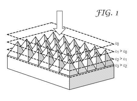
Fig. 1 depicts an embodiment of an electromagnetic wave isolator of the
present
invention.
Figs. 2a-21 depict different schematic cross-sections of embodiments of
electromagnetic wave isolators of the present invention made with two or more
materials.
Fig. 3 depicts an embodiment of an electromagnetic wave isolator of the
present
invention.
Fig. 4 depicts an embodiment of an electromagnetic wave isolator of the
present
invention having asymmetric stepped pyramid microstructured features.
Fig. 5 depicts a schematic cross-section of an embodiment of an
electromagnetic
wave isolator of the present invention having paraboloidal microstructured
features.
Fig. 6 depicts top and side views of an embodiment of an electromagnetic wave
isolator of the present invention.
Fig. 7 depicts an embodiment of an electromagnetic wave isolator of the
present
invention having tetrahedral microstructured features.
Fig. 8 depicts an embodiment of an electromagnetic wave isolator of the
present
invention having cylindrical post microstructured features.
Fig. 9 depicts a schematic cross-section of an embodiment of an
electromagnetic
wave isolator of the present invention having bimodal microstructured
features.
Fig. 10 depicts an embodiment of an RFID tag system including an
electromagnetic wave isolator of the present invention.
Fig. 11 depicts a graph comparing the thickness of isolators of the present
invention and comparative articles to their read ranges.
3
CA 02817214 2013-05-07
WO 2012/067846
PCT/US2011/059300
Fig. 12 depicts a graph comparing the thickness of isolators of the present
invention and comparative articles to their read ranges.
DETAILED DESCRIPTION
In the following description, reference is made to the accompanying set of
drawings that form a part of the description hereof and in which are shown by
way of
illustration several specific embodiments. It is to be understood that other
embodiments
are contemplated and may be made without departing from the scope or spirit of
the
present invention. The following detailed description, therefore, is not to be
taken in a
limiting sense.
Unless otherwise indicated, all numbers expressing feature sizes, amounts, and
physical properties used in the specification and claims are to be understood
as being
modified in all instances by the term "about." Accordingly, unless indicated
to the
contrary, the numerical parameters set forth in the foregoing specification
and attached
claims are approximations that can vary depending upon the desired properties
sought to
be obtained by those skilled in the art utilizing the teachings disclosed
herein. The use of
numerical ranges by endpoints includes all numbers within that range (e.g. 1
to 5 includes
1, 1.5, 2, 2.75, 3, 3.80, 4, and 5) and any range within that range.
One aspect of the present invention is an electromagnetic wave isolator having
at
least one microstructured surface or interface. The microstructured surface or
interface
provides a change in electromagnetic properties across the depth of the
microstructured
portion(s). The change may be a gradual change or a step change. The
electromagnetic
wave isolators of the present invention achieve this change in electromagnetic
properties,
at least in part, due to its physical features. This is in contrast to prior
art electromagnetic
wave isolators which achieve a change in electromagnetic properties across the
depth of
the isolator due to a change in electromagnetic properties of the materials
used to make
each layer of the isolator or by a compositional gradient within a specific
layer of the
isolator. Fig. 1 illustrates an electromagnetic wave isolator of the present
invention having
a pyramidal microstructured surface and indicates some exemplary planes of
equivalent
permittivity (8o; 81> co; c2> 81; and c3> 82) in the microstructured portion.
Other
electromagnetic properties, such as permeability, would correspondingly have
similar
variations. In at least one embodiment, the microstructured portion
effectively provides an
electromagnetic property gradient when at least one of the microstructured
features'
4
CA 02817214 2013-05-07
WO 2012/067846
PCT/US2011/059300
periodicity is, or periodicity and height are, less than the electromagnetic
wavelength
within the isolator material. For electromagnetic wavelengths much greater
than the
microstructured periodicity, the microstructured portion(s) will create a
medium in which
the electromagnetic property varies depending on the geometry of the surface
or interface
of the microstructured portion from that of free space (or a different
material) to that of the
base portion, i.e., the portion of the microstructured isolator section
adjacent to the
microstructured portion, made of the same material as the microstructured
portion but
containing no microstructured features. With proper matching of the
electromagnetic
properties, the microstructured pattern, the overall isolator thickness, and
the ratio of
microstructured portion thickness to base portion thickness, the reflectance
and/or isolator
characteristics of the construction can be enhanced for a particular antenna
design. For
electromagnetic frequencies in which the wavelength in the isolator medium is
less than
the periodicity of the microstructured pattern, in at least one embodiment of
the present
invention, the microstructured features serve as a method of changing the
effective
electromagnetic properties within that region in the isolator construction.
The wavelength
in the isolator medium is given by ko(841)-1/2. For an isolator with cr=300,
gr=1, and
microstructured features with a periodicity of 2 mm, the cut-off frequency is
about 9 GHz.
An isolator with a microstructured pyramidal array would behave as if it had a
continuously varying permittivity within the microstructured region for
electromagnetic
radiation lower than about 9 GHz. Above about 9 GHz, the microstructured
features will
behave more as discrete structures. For an isolator with cr=30, gr=1, and
microstructured
features with a periodicity of 0.3 mm, the cut-off frequency is about 200 GHz.
In at least one embodiment of the present invention, the microstructured
surface
creates (or provides) an interface that is not parallel to the overall plane
of the antenna, the
interface and adjacent three dimensional features of the isolator on both
sides of the
interface defining volumes comprising materials of contrasting electromagnetic
properties.
At least one embodiment of the electromagnetic wave isolator of the present
invention comprises a binder material loaded with a high permittivity and/or
high
permeability filler material formed into a construction such that at least one
surface has a
repeating array of features. The high permittivity and/or high permeability
filler-loaded
binder material can be formed into continuous microstructured films or sheets,
as in a
web-based process, or it can be utilized in a process producing individual
parts, such as
5
CA 02817214 2013-05-07
WO 2012/067846
PCT/US2011/059300
those designed for a very specific shape or application. Typically, the
material will
comprise about 80 wt% to about 95 wt% filler. However, the amounts are highly
dependent on the specific gravities of the binder and filler, as well as other
parameters
such as particle shape, compatibility of the particle with binder, type of
manufacturing
process, whether and what type of solvent is used, etc.
In at least one embodiment of the present invention, a binder (typically at a
small
concentration) can be blended with high permittivity or high permeability
material, the
microstructured pattern can be formed, the binder can be evaporated or burned
off, and the
construction can be sintered.
Suitable binders include thermoplastics, thermosets, curable liquids,
thermoplastic
elastomers, or other known materials for dispersing and binding fillers.
Specific suitable
materials include relatively non-polar materials such as polyethylene,
polypropylene,
silicone, silicone rubber, polyolefin copolymers, EPDM, and the like; polar
materials such
as chlorinated polyethylene, acrylate, polyurethane, and the like; and curable
materials
such as epoxies, acrylates, urethanes, and the like; and non-curable
materials. The binder
materials used to make the isolators of the present invention may be loaded
with different
types of low dielectric constant fillers, including glass bubbles, air (e.g.,
to create a foam),
and polytetrafluoroethylene (PTFE), such as TEFLON. PTFEs, such as TEFLON, may
also be used by itself as a binder. The materials used to make one or more
sections of the
isolators of the present invention may also be loaded with small concentration
of
compatibilizer-treated nanoparticles, such as those described in US Pat.
Publication No.
2008/ 0153963, blended with the high dielectric constant or high permeability
filler to
allow the filler to flow more freely and blend into a binder, if used,
allowing more
effective blending at higher concentrations of particles.
The materials used to make one or more sections of the isolators of the
present
invention may be loaded with soft magnetic materials such as ferrite materials
(CO2Z
from Trans-Tech Inc), an iron/silicon/aluminum material referred to by the
trade name
SENDUST but also available under other trade designations such as KOOL Mu
(Magnetics Inc, www.mag-inc.com), an iron/nickel material available under the
trade
designation PERMALLOY or its iron/nickel/molybdenum cousin MOLYPERMALLOY
from Carpenter Technologies Corporation (www.cartech.com), and carbonyl iron,
which
may be unannealed, annealed, and optionally treated with phosphoric acid or
some other
6
CA 02817214 2013-05-07
WO 2012/067846
PCT/US2011/059300
surface passivating agent. The soft magnetic material may have various
geometries such
as spheres, plates, flakes, rods, fibers, amorphous, and may be micro- or nano-
sized.
Alternatively, the materials used to make one or more sections of the
isolators of
the present invention may be loaded with different types of high dielectric
constant fillers,
including barium titanate, strontium titanate, titanium dioxide, carbon black,
or other
known high dielectric constant materials, including the carbon decorated
barium titanate
material described in U.S. Provisional Pat. App. No. 61/286247. Nano-sized
high
dielectric constant particles and/ or high dielectric constant conjugated
polymers may also
be used. Blends of two or more different high dielectric constant materials or
blends of
high dielectric constant materials and soft magnetic materials such as
carbonyl iron may
be used.
In at least one embodiment of the present invention, instead of using a binder
and
high dielectric constant material, an example of one suitable material is a
polyaniline/epoxy blend having a dielectric constant of around 3000 (J. Lu et
al., "High
dielectric constant polyaniline/epoxy composites via in situ polymerization
for embedded
capacitor applications", Polymer, 48 (2007), 1510-1516).
Microstructured patterns may be present on one outer surface of an isolator of
the
present invention; on both outer surfaces of the isolator with the same
pattern; or on both
outer surfaces of the isolator with different patterns and/or periodicities.
Microstructured
patterns may be present within the isolators of the present inventions at
interfaces of
sections comprising different materials. The microstructured patterns may be
present at
one or more interface within the isolator. If there is more than one
interface, the patterns
may be the same or different for the different interfaces. Figs. 2a-21
illustrate different
embodiments of the invention showing some of these variations. Fig. 2a shows
an article
with one microstructured surface. Fig. 2b shows an article with two opposing
microstructured surfaces. Fig. 2c shows an article with one microstructured
interface. An
interface is typically formed by creating a first section having
microstructured features on
a surface, then filling the open areas created by the microstructured features
with a
material different from the material forming the section having the
microstructured
surface. In at least one embodiment of the present invention, the different
material may
have a different permittivity and/or different permeability that the material
forming the
first section. The different material can be used to more finely tune the
isolator for an
7
CA 02817214 2013-05-07
WO 2012/067846
PCT/US2011/059300
intended application. In at least one embodiment of the present invention, the
materials
forming the first and second sections (and optionally additional sections)
will have
different permeabilities, the permeability values for the two sections having
a ratio of
about 3 to about 1000. In at least one embodiment of the present invention,
the materials
forming the first and second sections (and optionally additional sections)
will have
different permittivities, the permittivity values for the two sections having
a ratio of about
2.5 to about 1000. The different material may be any suitable material that
can provide
the desired electromagnetic properties, and includes but is not limited to,
polymers, resins,
adhesives, etc. They may optionally comprise a filler for tuning the
electromagnetic
properties of the system. As an alternative to filling the open areas with a
material, the
open areas can be left empty, in which case air functions as the different
material. See,
e.g., Figs. 2a and 2b. When the different material fills in the open areas
around the
microstructured surface (thus forming an interface), the electromagnetic
properties will
change from one outer surface of the article through to the other outer
surface in
accordance with the geometry of the microstructured surface or interface and
the
properties of the materials forming the various sections of the isolator. The
isolator may
optionally comprise an adhesive section on one or both outer surfaces or an
adhesive could
form an interior section between two non-adhesive sections. An adhesive may be
used as
the different material filling the open areas created by the microstructured
features. If the
material forming an outer surface of the isolator is not an adhesive, an
adhesive layer may
be applied to the isolator article to secure it to an object.
The isolator article may also include a metallic or conductive layer such that
regardless of the object against which the isolator and, e.g., an accompanying
tag or
antenna are placed, the antenna or tag would have the same read range. In such
a case, the
antenna-or-tag/isolator portion would be tuned to operate well with the
metallic layer
present, and the system would then operate equally well whether placed against
a metallic
article or a low permittivity material such as corrugated cardboard.
As previously stated, an article having one or more microstructured surfaces
or
interfaces may have two or more sections, the sections comprising materials
having
different permittivities and/or permeabilities. Fig. 2d illustrates an example
of a three
section/two interface article of the present invention in which each of the
three sections
comprises a different material and has different properties. Embodiments of
articles of the
8
CA 02817214 2013-05-07
WO 2012/067846
PCT/US2011/059300
present invention may have a myriad of different constructions. For example,
Figs. 2e and
2f illustrate articles of the present invention having the same total
thickness, but different
ratios of the materials that comprise the two sections of the article. Figs.
2g and 2h
illustrate articles of the present invention in which the ratios of the two
materials are the
same, but the overall thicknesses of the articles are different.
The microstructured features and the patterns of the microstructured features
may
also vary based on the particular embodiment of the invention. For example, in
articles
having the same overall thickness and same relative ratios of sections, the
length of the
gradient may differ, as illustrated in Figs. 2i and 2j. In other embodiments,
the lateral
spacing of microstructured features may also vary. For example, as illustrated
by Figs. 2k
and 21, the width and number of microstructured features may vary.
Microstructured features that provide a continuously varying electromagnetic
property gradient include features having surfaces non-horizontal and non-
vertical to a
major axis of the base portion of the section shaving such features. Exemplary
features
include, but are not limited to, pyramids, such as square-based pyramids (Fig.
3) having
acute, 900, or oblique vertex angles, triangular-based pyramids having acute,
oblique, or
cube corner vertex angles (Fig. 7), hexagonal based-pyramids, having acute or
oblique
vertex angles, rotated pyramids, and asymmetric pyramids, which may have
offset vertices
(e.g., sawtooth pyramids) cones such as cones having circular or ellipsoidal
bases, cones
having acute, 90 , or oblique vertex angles; paraboloids (Fig. 5), triangular
prisms (Fig. 6);
and hemispheres. Depending on the type of microstructure employed, the
electromagnetic
property gradient could vary linearly from one side of the construction to the
other. The
gradient could also be parabolic, or comprise other functionalities.
Microstructured features providing a step gradient in electromagnetic
properties
include those having surfaces horizontal and vertical to a major axis of the
base portion of
the section of the isolator having such features. Exemplary features include,
but are not
limited to, posts (Fig. 8) including those with round, square, and triangular
horizontal
cross-sections; parallelepipeds; and other similar block structures having
surfaces only
parallel and perpendicular (i.e., not sloped) to the base portion of the
section. In various
embodiments, the lateral spacing of microstructured features and the spacing
between the
bases of the individual microstructured features may vary.
9
CA 02817214 2013-05-07
WO 2012/067846
PCT/US2011/059300
Some microstructured features have multiple small step changes that
effectively
provide a gradient in electromagnetic properties. An example of such a
structure is the
asymmetric stepped pyramid in Fig. 4. Other examples would include shapes that
change
in multiple small increments.
Some microstructure features or patterns have shapes or arrangements that
provide
a combination of continuous and step gradients. For example, truncated
pyramids and
cones would provide a step gradient at its top (horizontal) surface but a
continuous
gradient at its side (sloped) surfaces. As another example, in the blade array
of Fig. 6, the
sloped surfaces of the triangular prisms would provide a continuous gradient
but the
vertical surfaces of the triangular prisms would provide a surface
perpendicular to the base
of the isolator..
In some embodiments, the patterns of the microstructured features of the
present
invention may be multi-modal, such as bimodal or trimodal with respect to
height (Fig. 9),
width, geometry, lateral spacing, periodicity, etc.
The resulting product may take a number of different forms, sometimes
depending
on the process used to make them. For example, a continuous sheet or web-based
process
may be used to produce a product in roll form, which can later be cut or sized
for specific
applications. The resulting product may be molded directly into distinct
shapes such as
rectangular, oval, or even complex 2-D geometries to minimize waste while
catering to a
specific product design.
Various methods of microstructuring are suitable for forming the
microstructured
surface or interface of the present invention. Suitable methods include
calendering; high
pressure embossing; casting and curing with a mold (e.g., using a high
permittivity or
permeability material with a binder, which binder is cured after the material
is cast on a
mold); compression molding (e.g., a mold and a high permittivity or
permeability material
with a binder are heated, then the mold is pressed against the material);
extrusion casting
(e.g., a high permittivity or permeability material with a binder is extruded
directly into a
heated tool, the tool is cooled, and the formed material is removed from the
tool);
extrusion embossing (e.g., a high permittivity or permeability material with a
binder is
extruded directly into a cold tool, then removed from the tool); flame
embossing (e.g., a
flame is used to heat just the surface of a high permittivity or permeability
material with a
binder, then the surface is microstructured with a tool); and injection
molding (e.g., molten
CA 02817214 2013-05-07
WO 2012/067846
PCT/US2011/059300
high permittivity or permeability material with a binder is injected into a
heated mold, then
cooled). Each of these systems could then have a material with a contrasting
electromagnetic property molded or cured over the microstructured portion.
Alternatively,
the initial microstructuring could be performed with a material possessing a
low
permeability and permittivity, and then a material having a contrasting
electromagnetic
property could be molded or cured over it.
Embodiments of the invention are suitable for use with antennae that operate
at
ultra high frequency or super high frequency regions. Embodiments of isolators
of the
present invention may be used in applications such as, but not limited to,
cell phones,
communication antennae, wireless routers, and RFID tags.
Embodiments of the invention find particular use in applications involving far-
field
electromagnetic radiation, such as when isolating RFID chips from metallic or
other
conductive surfaces. The isolators of the present invention are well-suited
for applications
using electromagnetic wavelengths that are much longer than the periodicity of
the
microstructured pattern or much longer than the microstructured pattern height
Aspects of this invention include systems using the isolators of this
invention to
isolate RFID tags from a conductive surface or body. Passive UHF RFID tag
antennas are
optimized for use in free space or on low dielectric materials, such as
corrugated
cardboard, pallet wood, etc. When a UHF RFID tag is in proximity to a
conductive
surface or body, the impedance and gain of the tag antenna changes, greatly
decreasing its
ability to power up and respond to the reader.
An isolator placed between the conductive substrate and RFID tag can
ameliorate
the effects of the metallic substrate by effectively increasing the distance
between the tag
and substrate (high permeability and/or permittivity), and by reducing the
ability of the
antenna's magnetic field from interacting with the conductive substrate (and
vice-versa).
The presence of the isolator can change not only the antenna gain, but also
the effective
impedance of the antenna, thus changing the amount of power transferred from
the
antenna to the RFID IC and, ultimately, the power modulated and backscattered
to the
RFID reader. Because of these and other complex interactions, isolator design
is specific
to a specific RFID tag. Similar arguments hold for other types of antennae
close to
conductive materials, such as a cell phone antenna proximate circuitry, or a
metallic
housing or ground plane.
11
CA 02817214 2013-05-07
WO 2012/067846
PCT/US2011/059300
RFID tags come in a myriad of different designs to meet a variety of customer
needs. Some of the differences in RFID IC design are related to their
differences in
power, memory, and calculation ability. RFID antenna design is dictated by a
number of
factors including the need to match impedances with the IC, desired read
distances,
footprint minimization, footprint aspect ratio, and orientation dependence on
response.
RFID tags of numerous designs can be purchased from any of a number of
companies,
such as Intermec Technologies Corporation, Alien Technology, Avery-Dennison,
and
UPM Raflatac.
A UHF RFID tag typically operates in the frequency range between 865 and 954
MHz, with the most typical center frequencies being 869 MHz, 915 MHz and 953
MHz.
The RFID tag can be self-powered by inclusion of a power source, such as a
battery.
Alternatively, it can be field-powered, such that it generates its internal
power by
capturing the energy of the electromagnetic waves being transmitted by the
base station
and converting that energy into a DC voltage.
The isolators of the present invention are most useful when the electrical
properties
of article to be tagged will interfere with the operation of the RFID tag.
This will most
often occur when the article to be tagged comprises a metal substrate, or is
configured to
contain liquids, which are both problematic with respect to read distances.
Fig. 10 illustrates a system of the present invention including an RFID tag
10, an
isolator 12 comprising sections 14 and 16, and an article to be tagged 18.
Adhesive layers
(not shown) may additionally be added between RFID tag 10 and section 14
and/or section
16 and article to be tagged 18, if the relevant isolator section 14, 16 does
not have
sufficient adhesive properties to adhere to the RFID tag or article to be
tagged 18.
EXAMPLES
This invention is illustrated by the following examples, but the particular
materials
and amounts thereof recited in these examples, as well as other conditions and
details
should not be construed to unduly limit this invention.
12
CA 02817214 2013-05-07
WO 2012/067846
PCT/US2011/059300
Test and Measurement Methods
Equivalent Thickness Calculation
"Equivalent thickness" means the thickness that a section would be if the
microstructured structures were flattened to create a solid section with no
microstructured
features.
NOTE: In all examples in which an RFID system was made, one layer of double
stick tape (SCOTCH 665, 3M Company) was adhered between the metal substrate
(either
an aluminum plate or 3MTm EMI Tin-Plated Copper Foil Shielding Tape 1183
(hereafter
sometimes referred to as "1183 Tape"), available from 3M Company) and the
isolator to
ensure the isolator remained adhered to the metal substrate.
Examples 1-3 and Comparative Examples (CE) A-F
Preparation of Comparative Examples A-F
TiO2 (TIPURE R-902+, Dupont Inc., www2.dupont.com) was blended into
silicone (SYLGARD 184, Dow Corning, www.dowcorning.com) at the rate of 58
weight
% TiO2 / 42 weight % silicone and cured into monolithic 2.5 cm x 10 cm slabs
at various
thicknesses. Carbonyl iron powder (ER Grade, BASF, www.inorganics.basf.com)
was
blended into silicone (SYLGARD 184, Dow Corning, www.dowcorning.com) at the
rate
of 85 weight % carbonyl iron / 15 weight % silicone and cured into monolithic
2.5 cm x
10 cm slabs at various thicknesses. Comparative Examples A through C had a 58%
TiO2 /
silicone blend section of 0.51 mm thick, and carbonyl iron / silicone blend
section
thicknesses of 0.72, 1.02, and 1.29 mm, respectively. Comparative Examples D
through F
had a 58% TiO2 / silicone blend section of 0.72 mm thick, and carbonyl iron /
silicone
blend section thicknesses of 0.48, 0.72, and 1.02 mm, respectively.
Preparation of Example 1
A nickel mold comprising 0.75 mm deep conical features arranged in a 0.65 mm
hexagonal close-packed spacing was fabricated. The hexagonal close-packed
array
covered a 2.5 cm x 10 cm area. 58% by weight TiO2 (TIPURE R-902+, Dupont Inc.,
www2.dupont.com) was blended into a silicone system (SYLGARD 184, Dow Corning,
www.dowcorning.com), cured in the mold, and then removed. The thickness of the
TiO2 /
silicone base portion below the cones was 0.28 mm thick. With the 0.75 mm high
cones,
the equivalent thickness of the overall TiO2 section was 0.53 mm. Then, 85% by
weight
13
CA 02817214 2013-05-07
WO 2012/067846
PCT/US2011/059300
carbonyl iron powder (ER Grade, BASF, www.inorganics.basf.com) was blended
into
silicone (SYLGARD 184, Dow Corning, www.dowcorning.com) and the blend was
applied to fill the space around and just above the Ti02-filled cones. To
create a smooth
surface, the blend was added beyond the tops of the 0.75 mm tall cones by
about 0.29 mm.
Subsequently, the blend was cured.
Preparation of Examples 2-3
Monolithic slabs prepared in the same manner as for Comparative Examples A-F
having 85 weight % ER Grade carbonyl iron / 15% silicone were placed against
the
carbonyl iron side of Example 1 to increase the thickness of the carbonyl iron
section for
Examples 2 and 3. The monolithic slab thicknesses for Examples 2 and 3 were
0.27 mm
and 0.48 mm, respectively. No adhesive was necessary to hold the finished
article
together due to the adhesion properties of the silicone.
RFID Systems using Comparative Examples A-F and Examples 1-3
RFID tag systems using Comparative Examples A-F and Examples 1-3 were made
using Avery Dennison 210 Runway RFID tags operating with the Gen 2 protocol.
The
tags were read from 902-928 MHz proximate a 12.5 mm thick aluminum plate. The
RFID
tag system was constructed with the following sequence of adjacent sections:
aluminum
plate / Ti02-filled section of isolator / carbonyl iron-filled section of
isolator / RFID tag.
This system was moved at various positions in front of an ALR-9780 Alien
Reader until a
75% RFID tag read rate was obtained. For each Comparative Example and Example,
the
distance from the ALR-9780 reader at a 75% read rate was determined at three
independent readings and then averaged.
The read range data for the Comparative Examples are shown in Table 1. The
second and third columns show the actual thicknesses of the TiO2 / silicone
blend section
and the carbonyl iron / silicone blend sections, respectively. Table 1 shows
that the read
range increased monotonically as the carbonyl iron section thickness increased
from 0.72
to 1.29 mm for a TiO2 section thickness of 0.51 mm. Similarly, the read range
increased
monotonically as the carbonyl iron section thickness increased from 0.48 to
1.02 mm
when the TiO2 section was 0.73 mm thick.
The read range data for the Examples are shown in Table 2. The second and
third
columns give equivalent thicknesses of the TiO2 and carbonyl blend sections,
respectively. The read range increased monotonically as the equivalent
carbonyl iron
14
CA 02817214 2013-05-07
WO 2012/067846
PCT/US2011/059300
section thickness increased from 0.79 to 1.27 mm with an effective TiO2
section thickness
of 0.53 mm.
The read range versus isolator thickness for comparative Examples A-F and
Examples 1-3 are plotted together in Figure 11. The data points on the solid
line
represent, from left to right, Examples 1, 2, and 3. The data points on the
line with large
dashes represent, from left to right, Comparative Examples A, B, and C. The
data points
on the line with small dashes represent, from left to right, Comparative
Examples D, E,
and F. Comparative Examples A - C comprise a TiO2 section thickness
essentially
equivalent to that of Examples 1 - 3. It is clear that, at any given isolator
thickness,
Examples 1 - 3 provide a longer read range than that of Comparative Examples A
- C.
Increasing the TiO2 section thickness in the Comparative Examples did not show
a
substantial increase in the read distance, as illustrated in Fig. 11.
Table 1
Total
Carbonyl Iron Read
TiO2 Section Carbonyl Iron Section Thickness Section
Range
Example Thickness (mm) Thickness (mm) (mm)
Fraction (cm)
CE A 0.51 0.72 1.23 0.59
46
CE B 0.51 1.02 1.53 0.67
82
CE C 0.51 1.29 1.80 0.72
85
CE D 0.73 0.48 1.21 0.40
27
CE E 0.73 0.72 1.45 0.50
71
CE F 0.73 1.02 1.75 0.58
88
Table 2
Effective Carbonyl Iron Total Carbonyl
Read
Effective TiO2 Section Section Thickness
Thickness Iron Section Range
Example Thickness (mm) (mm) (mm) Fraction
(cm)
1 0.53 0.79 1.32 0.60
75
2 0.53 1.06 1.59 0.67
95
3 0.53 1.27 1.80 0.71
99
Examples 4-6 and Comparative Examples (CE) G-0
Preparation of Comparative Examples G-0
XLD3000 glass bubbles (3M Company, www.3m.com) were blended into silicone
(SYLGARD 184, Dow Corning, www.dowcorning.com) at the rate of 15 weight %
XLD3000 / 85 weight % silicone and cured into monolithic 2.5 cm x 10 cm slabs
at
various thicknesses. Carbonyl iron powder (ER Grade, BASF,
www.inorganics.basf.com)
CA 02817214 2013-05-07
WO 2012/067846
PCT/US2011/059300
was blended into silicone (SYLGARD 184, Dow Corning, www.dowcorning.com) at
the
rate of 85 weight % carbonyl iron / 15 weight % silicone and cured into
monolithic 2.5 cm
x 10 cm slabs at various thicknesses. Comparative Examples G through I had a
15 weight
% XLD3000 / silicone blend section thickness of 0.41 mm, and carbonyl iron /
silicone
blend section thicknesses of 0.72, 1.02, and 1.29 mm, respectively.
Comparative
Examples J through L had a 15 weight % XLD3000 / silicone blend section
thicknesses of
0.49 mm, and carbonyl iron / silicone blend section thicknesses of 0.72, 1.02,
and 1.29
mm, respectively. Comparative Examples M through 0 had a 15 weight % XLD3000 /
silicone blend section thickness of 0.54 mm, and carbonyl iron / silicone
blend section
thicknesses of 0.72, 1.02, and 1.29 mm, respectively.
Preparation of Examples 4
A nickel mold comprising 0.36 mm deep pyramidal features arranged in a 0.59 mm
square spacing was fabricated. 85% by weight carbonyl iron powder (ER Grade,
BASF,
www.inorganics.basf.com) was blended into a silicone system (SYLGARD 184, Dow
Corning, www.dowcorning.com), cured in the mold, then removed. The thickness
of the
carbonyl iron / silicone base portion below the pyramids was 0.70 mm thick.
With the
0.36 mm high pyramids, the equivalent thickness of the overall carbonyl iron
section was
0.82 mm. 15% by weight XLD3000 glass bubbles (3M Company, www.3m.com) blended
into a silicone system (SYLGARD 184, Dow Corning, www.dowcorning.com) was
applied to fill the space around and to 0.22 mm above the carbonyl iron filled
pyramids
and then cured. The total actual thickness of Example 4 was 1.28 mm.
Preparation of Examples 5-6
Monolithic slabs of 85 weight % ER Grade carbonyl iron / 15% silicone were
placed against the carbonyl iron side of Example 4 to increase the thickness
of the
carbonyl iron section to create Examples 5 and 6. The monolithic slab
thicknesses for
Examples 2 and 3 were 0.27 mm and 0.48 mm, respectively. No adhesive was
necessary
to hold the finished article together due to the adhesion properties of the
silicone.
RFID Systems using Comparative Examples G-0 and Examples 4-6
RFID tag systems using Comparative Examples G-0 and Examples 4-6 were made
using UPM Rafsec G2, ANT ID 17B1, IMPINJ MONZA tags operating with the Gen 2
protocol. The tags were read from 902 to 928 MHz proximate a 12.5 mm thick
aluminum
16
CA 02817214 2013-05-07
WO 2012/067846
PCT/US2011/059300
plate. The RFID tag system was constructed with the following sequence of
adjacent
sections: aluminum plate / carbonyl iron-filled section of isolator/ glass
bubble filled
section of isolator! RFID tag. The system was moved at various positions in
front of an
ALR-9780 Alien Reader until a 75% RFID tag read rate was obtained.
The read range data for the Comparative Examples are displayed in Table 3. The
second and third columns show the thicknesses of the glass bubble / silicone
blend section
and the carbonyl iron! silicone blend sections, respectively. Table 3 shows
that the read
range increased monotonically as the carbonyl iron section thickness increased
from 0.72
to 1.29 mm for glass bubble section thicknesses of 0.41 and 0.49 mm. The read
range for
the 0.54 mm thick glass bubble section increased up to 50 cm as the carbonyl
iron section
thickness increased from 0.72 to 1.29 mm.
The read range data for Examples 4-6 of the invention are shown in Table 4.
The
second and third columns give equivalent thicknesses of the glass bubble and
carbonyl
iron blend sections, respectively. The UPM Rafsec IMPINJ MONZA tag read range
increased monotonically as the equivalent carbonyl iron section thickness
increased from
0.82 to 1.30 mm while the glass bubble section thickness remained constant at
0.46 mm.
The read range versus isolator thickness for comparative Examples G-0 and
Examples 4-6 are plotted together in Figure 12. The data points on the solid
line with
solid circles represent, from left to right, Examples 4, 5, and 6. The data
points on the line
with large dashes represent, from left to right, Comparative Examples G, H,
and I. The
data points on the solid line with hollow squares represent, from left to
right, Comparative
Examples J, K, and L. The data points on the line with small dashes represent,
from left to
right, Comparative Examples M, N, and 0. Comparative Examples G-0 comprise
glass
bubble section thicknesses essentially the same, and just above and below that
of
Examples 4-6. It is clear that, at any given isolator thickness, Examples 4-6
provide a
longer read range than that provided by the equivalent isolator thickness of a
sectioned
system. Changing the glass bubble section thickness within the range 0.41 to
0.54 mm in
the Comparative Examples does not substantially change the read distance, as
illustrated in
the graph.
17
CA 02817214 2013-05-07
WO 2012/067846
PCT/US2011/059300
Table 3
Carbonyl Iron Total Carbonyl Iron
Glass Bubble Section Section Thickness Thickness
Section Read
Example Thickness (mm) (mm) (mm) Fraction
Range (cm)
CE G 0.41 0.72 1.13 0.64 32
CE H 0.41 1.02 1.43 0.71 49
CE I 0.41 1.29 1.70 0.76 55
CE J 0.49 0.72 1.21 0.60 32
CE K 0.49 1.02 1.51 0.68 48
CE L 0.49 1.29 1.78 0.72 49
CE M 0.54 0.72 1.26 0.57 39
CE N 0.54 1.02 1.56 0.65 50
CE 0 0.54 1.29 1.83 0.70 50
Table 4
Effective Glass Effective Carbonyl Total
Bubble Section Iron Section Thickness Carbonyl Iron Read
Example Thickness (mm) Thickness (mm) (mm) Section Fraction
Range (cm)
4 0.46 0.82 1.28 0.64 49
0.46 1.09 1.55 0.70 57
6 0.46 1.30 1.76 0.74 62
Examples 7-8 and Comparative Examples P-S
Preparation of Comparative Examples P-S
5 BaTiO3 (TICON P, TAM Ceramics, now Ferro Corp., www.ferro.com) was
blended into silicone (SYLGARD 184, Dow Corning, www.dowcorning.com) at the
rate
of 73.6 weight % BaTiO3 / 26.4 weight % silicone and cured into monolithic 2.5
cm x 10
cm slabs at various thicknesses. XLD3000 glass bubbles (3M Company,
www.3m.com)
were blended into silicone (SYLGARD 184, Dow Corning, www.dowcorning.com) at
the
rate of 15 weight % XLD3000 / 85 weight % silicone and cured into monolithic
2.5 cm x
10 cm slabs at various thicknesses. Comparative Examples P and Q had a 15 wt %
XLD3000 glass bubble / silicone blend section thickness of 0.68 mm and a 73.6
wt %
BaTiO3 / silicone blend section of 1.81 mm thick. Comparative Examples R and S
had a
wt % XLD3000 glass bubble / silicone blend section thickness of 0.63 mm and a
73.6
15 wt % TICON P / silicone blend section of 1.90 mm thick.
Preparation of Examples 7-8
A nickel mold comprising 0.68 mm deep paraboloidal features arranged in a 0.65
mm hexagonal close-packed spacing was fabricated. The hexagonal close-packed
array
18
CA 02817214 2013-05-07
WO 2012/067846
PCT/US2011/059300
covered a 2.5 cm x 10 cm area. 15% by weight % XLD3000 glass bubbles were
blended
into a silicone system (SYLGARD 184, Dow Corning, www.dowcorning.com), cured
in
the mold, and then removed. The thickness of the XLD3000 / silicone base below
the
paraboloids was 0.31 mm thick. With the 0.68 mm high paraboloids, the
equivalent
thickness of the overall XLD3000 section was 0.65 mm. 73.6% by weight TICON P
was
blended into silicone, applied to fill in the space around and 1.49 mm, above
the
XLD3000-filled paraboloids, and cured to create Examples 7 and 8.
RFID Systems using Comparative Examples P-S and Examples 7-8
RFID tag systems using Comparative Examples P-S and Examples 7-8 were made
with Alien ALN-9654-FWRW tags operating with the Gen 2 protocol. The tags were
read
from 902-928 MHz proximate a foil tape (1183 Tape, 3M Company, www.3m.com) but
arranged in different orientations with respect to the foil tape and the RFID
tag. The RFID
tag system was constructed with different sequences of adjacent sections for
different
samples, as further described below. The isolator/tag construction was
centered in the
middle of the 75 mm x 125 mm foil tape. The tag was placed 0.80 meters from a
transmitting/receiving antenna powered by a SAMSys MP9320 2.8 UHF RFID reader.
The percentage of successful reads over a series of 4 separate scans across
the 920-928
MHz spectrum at maximum reader power was calculated.
In the RFID systems using Comparative Examples P and Q and in Example 7, the
TICON P-filled section was oriented toward the foil tape. In the RFID systems
using
Comparative Examples R and S and in Example 8, the TICON P-filled section was
oriented toward the RFID tag. The read rate data for the Comparative Examples
are
displayed in Table 5. Read rate data for the Examples are displayed in Table
6.
Table 5 illustrates that, for a glass bubble / silicone blend sectioned with a
barium
titanate / silicone blend at a total thickness of about 2.5 mm and a barium
titanate / silicone
blend fraction of 0.74, the read rates are very poor when the barium titanate-
filled section
is oriented toward the foil tape. When the barium titanate-filled section is
oriented toward
the RFID tag, the read rate is still poor when the barium titanate section
fraction is only
0.73 and the total thickness is 2.49 mm. When the total thickness is increased
to 2.53 mm
while further increasing the barium titanate section fraction to 0.75, the
read rate increases
to 69%. In this instance, the orientation of the comparative isolator
construction can
therefore be very important.
19
CA 02817214 2013-05-07
WO 2012/067846
PCT/US2011/059300
Table 6 shows that Examples 7 and 8 perform better than their Comparative
Example sectioned counterparts. When the barium titanate-filled section is
oriented
toward the foil tape, the read rate is far superior for Example 7 vs.
Comparative Examples
P and Q. When the barium titanate-filled section is oriented toward the RFID
tag, the read
rate is still shown to be better for Example 8 vs. Comparative Examples R and
S. In fact,
Examples 7 and 8 both perform better than any of Comparative Examples P to S.
Table 5
Glass Bubble TICON P
TICON P Section Section Total TICON P
Section Thickness Thickness Thickness Section
Read
Example Against (mm) (mm) (mm) Fraction
Rate
CE P Metal 0.68 1.81 2.49 0.73
<2%
CE Q Metal 0.63 1.90 2.53 0.75
14%
CE R Tag 0.68 1.81 2.49 0.73
<2%
CE S Tag 0.63 1.90 2.53 0.75
69%
Table 6
Effective
TICON P
TICON P Effective Section Total TICON P
Section Glass Bubble Thickness Thickness
Section Read
Example Against Section (mm) (mm) (mm) Fraction
Rate
7 Metal 0.65 1.83 2.48 0.74
73%
8 Tag 0.65 1.83 2.48 0.74
76%
Example 9
Preparation of Example 9
A nickel mold comprising inverse asymmetric pyramids was created utilizing
conventional stereolithography techniques followed by nickel plating. The apex
of the
pyramid was fabricated directly over one corner of the pyramid base (see,
e.g., Fig. 4), and
a square array of these pyramids was created with all apexes in the same
orientation. The
stair-stepped features of the asymmetric pyramids created a series of 10 steps
on a 1.21
mm square base. Fifteen weight percent XLD3000 glass bubbles were blended into
SYLGARD 184, cured in the mold, and then removed. The height of these stair-
stepped,
asymmetric pyramids comprising the XLD3000/silicone blend was 0.546 mm. The
thickness of the XLD3000 / silicone base portion below the asymmetric pyramids
was
0.134 mm. With the 0.546 mm high asymmetric pyramids, the equivalent thickness
of the
overall XLD3000/silicone section was 0.32 mm. Eighty-five weight percent ER
Grade
CA 02817214 2013-05-07
WO 2012/067846
PCT/US2011/059300
carbonyl iron powder was blended into SYLGARD 184 and then cured. This
isolator
construction was trimmed to a 45 x 100 mm area. The total thickness of the
finished
article was 1.50 mm.
RFID System using Example 9
An RFID tag systems using Example 9 was made with an RSI-122 dual dipole tag
(40 x 80 mm) operating with the Gen 2 protocol. The tag was held in place on
the isolator
by a combination of the natural adhesion properties of the silicone and a thin
strip of tape
over the top of the tag. The tag was read from 902-928 MHz proximate a foil
tape (1183
Tape) in an anechoic chamber. The isolator/tag construction was centered in
the middle of
a 75 mm x 125 mm piece of foil tape with the carbonyl iron section against the
foil tape.
The tag was placed 0.70 meters from a transmitting/receiving antenna powered
by a
SAMSys MP9320 2.8 UHF RFID reader. The minimum power required to obtain a
response from the tag was determined across the 920-928 MHz spectrum and
averaged
over 4 separate scans.
With overall thickness of the isolator construction at 1.50 mm, the equivalent
thickness of the carbonyl iron section was 1.18 mm, and the equivalent
thickness of the
XLD3000 section was 0.32 mm. The tag / isolator / foil tape construction was
read
successfully across the entire spectrum, with an average minimum power of 26.9
dBm
from the SAMSys reader.
Example 10
Preparation of Example 10
A nickel mold comprising inverse paraboloids of two different heights and
widths
was created. Fifteen weight percent XLD3000 glass bubbles were blended into
SYLGARD 184, cured in the mold, and then removed. The larger paraboloid
cavities
created features 0.765 mm in height and 0.590 mm base width. The smaller
paraboloid
cavities created features 0.250 mm in height and 0.323 mm in base width. These
two
disparate-sized and -aspect ratio paraboloids were arranged in a regularly
alternating
square array with a unit cell length of 1.192 mm. The thickness of the XLD3000
/ silicone
base portion below the bimodal distribution of paraboloids was 0.201 mm. With
the
bimodal distribution of paraboloids, the equivalent thickness of the overall
XLD3000/silicone section was 0.363 mm. Eighty-five weight percent R1521
carbonyl
iron powder (ISP Corp, www.ispcorp.com) was blended into SYLGARD 184, applied
to
21
CA 02817214 2013-05-07
WO 2012/067846
PCT/US2011/059300
fill in the space around and 0.254 mm above, the XLD3000-filled paraboloids,
and then
cured. This isolator construction was trimmed to a 25 x 100 mm area.
RFID System using Example 10
An RFID tag systems using Example 10 was made with an ALN-9654 tag
operating with the Gen 2 protocol. The tag was held in place on the isolator
by a
combination of the natural adhesion properties of the silicone and a thin
strip of tape over
the top of the tag. The tag was read from 902-928 MHz proximate a foil tape
(1183 Tape)
in an anechoic chamber. The isolator/tag construction was centered in the
middle of a 75
mm x 125 mm piece of the foil surface with the carbonyl iron section against
the RFID
tag. The tag was placed 0.80 meters from a transmitting/receiving antenna
powered by a
SAMSys MP9320 2.8 UHF RFID reader. The minimum power required to obtain a
response from the tag was determined across the 920-928 MHz spectrum and
averaged
over 4 separate scans.
With the overall thickness of the isolator construction at 1.22 mm, the
equivalent
thickness of the carbonyl iron section was 0.86 mm, and the equivalent
thickness of the
XLD3000 section was 0.36 mm. The tag / isolator / foil tape construction was
read
successfully across the entire spectrum, with an average minimum power of 25.7
dBm
from the SAMSys reader.
Example 11
Preparation of Example 11
An anisotropic, flake-shaped high permeable ferrite filler material (91wt%)
was
mixed with an acrylate copolymer binder (9 wt%). Ten parts by weight Co2Z-K
ferrite
(Trans-Tech Inc, www.trans-techinc.com) was blended with 0.98 parts by weight
acrylate
copolymer (90 weight percent isooctyl acrylate / 10 weight percent acrylic
acid) and 6.41
parts by weight solvent (50 weight percent heptane / 50 weight percent methyl
ethyl
ketone). This solution was cast, dried, and then hot pressed to remove any
entrained
voids. A CO2 laser was used to drill 0.70 mm diameter holes forming a 1.30 mm
square
array into a 0.85 mm thick slab of this 91 weight percent ferrite / 9 weight
percent acrylate
copolymer material. A 0.52 mm thick slab of the same material was created, and
both
constructions were trimmed to 25 x 100 mm and adhered together by pressing the
somewhat pressure sensitive adhesive slabs together.
22
CA 02817214 2013-05-07
WO 2012/067846
PCT/US2011/059300
RFID System using Example 11
An RFID tag systems using Example llwas made with an ALN-9654 tag
operating with the Gen 2 protocol. The tag was held in place on the isolator
by a
combination of the natural adhesion properties of the acrylate and a thin
strip of tape over
the top of the tag. The tag was read from 902-928 MHz proximate a foil tape
(1183 Tape)
in an anechoic chamber. The isolator/tag construction was centered in the
middle of a 75
mm x 125 mm 1183 piece of foil tape with the 0.52 mm thick monolithic
ferrite/acrylate
slab against the foil tape and the 0.85 mm thick slab with the unfilled
drilled holes against
the RFID tag. The tag was placed 0.80 meters from a transmitting/receiving
antenna
powered by a SAMSys MP9320 2.8 UHF RFID reader. The minimum power required to
obtain a response from the tag was determined across the 920-928 MHz spectrum
and
averaged over 8 separate scans.
With an overall thickness of the isolator construction at 1.37 mm, the
equivalent
thickness of the ferrite section was 1.18 mm, and the equivalent thickness of
the air section
was 0.19 mm. The tag / isolator / foil tape construction was read successfully
across the
entire spectrum, with an average minimum power of 23.8 dBm from the SAMSys
reader.
Example 12
Preparation of Example 12
133.5 grams ER Grade carbonyl iron powder was blended with 19.95 grams
thermoplastic polymer ENGAGE 8401 (The Dow Chemical Company, www.dow.com ) in
a Haake mixer at 150 C. This material was pressed into a nickel mold
comprising
inverted pyramids at 150 C to produce a carbonyl iron/thermoplastic blend
isolator with a
flat surface on one side and microstructured surface having pyramidal
projections on the
other side. The length and spacing of these pyramids was 0.588 mm and the
pyramid
height was 0.349 mm. The total thickness of the construction was 0.98 mm. The
sample
was trimmed to 25 x 100 mm.
RFID System using Example 12
An RFID tag systems using Example 12 was made with an ALN-9654 tag
operating with the Gen 2 protocol. The tag was held in place on the isolator
by a thin strip
of tape over the top of the tag. The tag was read from 902-928 MHz proximate a
foil tape
(1183 Tape) in an anechoic chamber. The isolator/tag construction was centered
in the
middle of a 75 mm x 125 mm 1183 piece of foil tape with the microstructured
surface of
23
CA 02817214 2013-05-07
WO 2012/067846
PCT/US2011/059300
the isolator facing the foil tape. The tag was placed 0.80 meters from a
transmitting/receiving antenna powered by a SAMSys MP9320 2.8 UHF RFID reader.
The minimum power required to obtain a response from the tag was determined
across the
920-928 MHz spectrum and averaged over 4 separate scans.
The equivalent thickness of the carbonyl iron/thermoplastic section was 0.75
mm,
and the equivalent thickness of the air section surrounding the pyramids was
0.23 mm.
The tag / isolator / foil tape construction was read successfully across the
entire spectrum,
with an average minimum power of 27.7 dBm from the SAMSys reader.
Example 13
Preparation of Example 13
A nickel mold comprising tetrahedra on a hexagonal close packed lattice was
created. Eighty-five weight percent HQ grade carbonyl iron powder (BASF,
www.inorganics.basf.com) was blended into SYLGARD 184 and then cured in this
mold
to create tetrahedral indentations in the surface of the carbonyl iron /
silicone blend
section. The indentations were 0.20 mm deep and 0.29 mm from apex to apex. The
overall thickness of this isolator construction was 1.04 mm. This isolator was
trimmed to
a 25 x 100 mm area.
RFID System using Example 13
An RFID tag systems using Example 13 was made with an ALN-9654 tag
operating with the Gen 2 protocol. The tag was held in place on the isolator
by a thin strip
of tape over the top of the tag. The tag was read from 902-928 MHz proximate a
foil tape
(1183 Tape) in an anechoic chamber. The isolator/tag construction was centered
in the
middle of a 75 mm x 125 mm 1183 Tape foil surface with the carbonyl iron
section
against the RFID tag. The tag was placed 0.80 meters from a
transmitting/receiving
antenna powered by a SAMSys MP9320 2.8 UHF RFID reader. The minimum power
required to obtain a response from the tag was determined across the 920-928
MHz
spectrum and averaged over 4 separate scans.
With an overall thickness of the isolator construction at 1.04 mm, the
equivalent
thickness of the carbonyl iron section was 0.97 mm, and the equivalent
thickness of the air
section was 0.07 mm. The tag / isolator / foil tape construction was read
successfully
across the entire spectrum, with an average minimum power of 19.5 dBm from the
SAMSys reader.
24
CA 02817214 2013-05-07
WO 2012/067846
PCT/US2011/059300
Example 14
Preparation of Example 14
EW-I Grade carbonyl iron powder (BASF, www.inorganics.basf.com) at 94.2
weight percent was blended into a polyolefin available under the trade
designation
ADFLEX V 109 F (Lyondell Base11, www.alastian.com ) in a Brabender batch mixer
at
160 C, then pressed into a flat sheet. Two nickel molds identical to those
used in Example
13 were utilized to press the flat sheet into an isolator comprising
microstructured
tetrahedral indentations on both sides. The overall thickness of this
construction was 0.69
mm. This isolator was trimmed to a 25 x 100 mm area.
RFID System using Example 13
An RFID tag systems using Example 13 was made with an ALN-9654 tag
operating with the Gen 2 protocol. The tag was held in place on the isolator
by small
strips of tape over the top of the tag. The tag was read from 902-928 MHz
proximate a
foil tape (1183 Tape) in an anechoic chamber. The isolator/tag construction
was centered
in the middle of a 75 mm x 125 mm foil tape with the carbonyl iron section
against the
RFID tag. The tag was placed 0.80 meters from a transmitting/receiving antenna
powered
by a SAMSys MP9320 2.8 UHF RFID reader. The minimum power required to obtain a
response from the tag was determined across the 920-928 MHz spectrum and
averaged
over 4 separate scans.
With an overall thickness of the isolator construction at 0.69 mm, the
equivalent
thickness of the carbonyl iron section was 0.56 mm, and the equivalent
thickness of the air
section on each side was 0.07 mm. The tag / isolator / foil tape construction
was read
successfully across the entire spectrum, with an average minimum power of 20.3
dBm
from the SAMSys reader.
Although specific embodiments have been illustrated and described herein for
purposes of description of the preferred embodiment, it will be appreciated by
those of
ordinary skill in the art that a wide variety of alternate and/or equivalent
implementations
may be substituted for the specific embodiments shown and described without
departing
from the scope of the present invention. This application is intended to cover
any
adaptations or variations of the preferred embodiments discussed herein.
Therefore, it is
manifestly intended that this invention be limited only by the claims and the
equivalents
thereof