Note: Descriptions are shown in the official language in which they were submitted.
CA 02817934 2013-05-28
TRANSMISSION OF INFORMATION FROM
AN IMPLANTED MEDICAL DEVICE
TECHNICAL FIELD
This invention relates to devices that require the
transfer of energy from a power source apparatus outside the
body to an implanted medical device apparatus located inside
the body, and more particularly to the transmission of
information from the implanted apparatus to the power source
apparatus, for example, to regulate the power supplied by
the power source apparatus.
BACKGROUND
A transcutaneous energy transfer system (TETS) provides
a means of transferring electrical energy from an external
power supply apparatus to an implanted medical device
through the skin of the patient. In a typical TETS, energy
is transferred by magnetically coupling an external coil,
located in the external power supply apparatus, to an
internal coil associated with the implanted medical device.
Implanted devices receiving power from an external
source typically require a load voltage within a specified
operating range. An implanted blood pump may require, for
example, a load voltage of not less than twelve volts, but
no more than fifteen volts. The external power supply
apparatus therefore needs to deliver the appropriate amount
of energy to the implanted device so that the load voltage
remains within the specified operating range. The load
voltage level at any given time is determined by the amount
of energy being transferred from the external power supply
apparatus, the efficiency of the magnetic coupling between
1
CA 02817934 2013-05-28
the external and internal coils, and the load imposed by the
implanted medical device. The positioning of the external
coil relative to the internal coil affects the efficiency of
the magnetic coupling, and if the magnetic coupling is less
than optimal, the external power supply apparatus may need
to transmit more energy to maintain the load voltage within
the specified operating range. The magnetic coupling
efficiency may also change over time because, for example,
patient movement may result in a change in position of the
external coil relative to the internal coil, or because of
the presence of an electromagnetic signal interfering with
the efficiency of the magnetic coupling. Of course,
fluctuations in the operation of the implanted device occur,
and thus the load imposed by the medical device typically
will vary over time.
To regulate the load voltage level, a feedback signal
indicating the present load voltage level may be
communicated from the implanted apparatus to the external
power supply apparatus. One known method of providing this
feedback information involves the transmission of radio
frequency (RF) signals from the implanted device to the
external power supply apparatus, which requires RE'
transmitters and receivers. Another known method involves
transmitting an infrared signal with the feedback
information through the patient's skin. Yet another method
is to add coils to the external apparatus and the implanted
apparatus, in addition to the power transfer coils, to
transmit the feedback signal from the implanted device to
the external power supply apparatus.
In addition to feedback information being transmitted
to regulate the load voltage level, other information may
2
CA 02817934 2013-05-28
also be transmitted from an implanted medical device. For
example, other information that may be transmitted may
include telemetry or other logic information such as, in the
case of a blood pump being the load-generating device, an
indication that the pump is operating properly or is in
fault, that an internal battery is fully charged or not, or
whether the pump is operating on main or redundant
components.
SUMMARY
The invention, in one general aspect, features a
medical TETS that provides feedback information from an
implanted medical device to an external power source using
the same coils over which power is transferred from the
external power source to the implanted medical device.
In an aspect, an implantable device that requires
electrical power from an external power source for operation
has an inductor-capacitor (LC) tank circuit that receives
power from the external source and delivers the power to a
load-generating device. Feedback circuitry senses a load
voltage level of the power delivered to the load-generating
device and produces a feedback signal indicative of the load
voltage level. The feedback signal is superimposed on the
LC tank circuit for communication to the external power
source.
The feedback signal, in one implementation, comprises a
series of pulses at varying frequencies indicative of the
load voltage level. The pulses may be generated at varying
frequencies within a specified range with a center
frequency, for example, one kilohertz. The center frequency
may indicate that the load voltage level is the desired
level and no adjustment needs to be made to the amount of
3
CA 02817934 2013-05-28
power the external power source is delivering, while
frequencies above and below the center frequency may
indicate that the amount of power the external power source
is delivering needs to be adjusted to bring the load voltage
level back to the desired level.
The feedback circuitry may have a voltage-to-frequency
converter. The voltage-to-frequency converter may include
an error amplifier that compares the load voltage level to a
reference voltage and generates a difference signal, and a
controller to receive the difference signal and generate the
feedback signal. The feedback circuitry may also have a
switch that receives the feedback signal, and that is
coupled with the LC tank circuit so that during the time the
feedback signal is pulsed high the switch closes and the LC
tank circuit is short-circuited to superimpose the feedback
signal on the LC tank circuit.
The implanted medical device may also include a
rectifier that includes first and second diodes having a
forward bias directed toward a positive terminal of the
load-generating device. The first diode may be coupled to a
first terminal of the LC tank circuit and the second diode
coupled to a second terminal of the LC tank circuit. The
rectifier may also have first and second transistor switches
whose current conducting terminals are coupled,
respectively, between the first terminal of the LC tank
circuit and negative terminal of the load-generating device
and between the second terminal of the LC tank circuit and
the negative terminal of the load-generating device. The
first and second transistor switches may serve as the
switch, each receiving the feedback signal at their gates
and being activated by pulses in the feedback signal.
4
CA 02817934 2013-05-28
In another aspect, the invention features an external
power source for an implantable device. An electrical power
source is provided. A pulse-width modulator and driver
generates a power signal that is transmitted over an LC tank
circuit. A sensor senses a feedback signal indicative of a
load voltage level that is provided by the implantable
device through the LC tank circuit. The external power
source varies the amount of power delivered to the
implantable device in response to the feedback signal.
lo The external power source may also include a decoder
that receives the sensed feedback signal, determines the
frequency of the pulses in the feedback signal, and
generates a voltage signal indicative of the frequency of
the pulses in the feedback signal. The feedback signal
sensed by the external power source may, as discussed
previously, comprise a series of pulses, the frequency that
the pulses are generated being indicative of the load
voltage level. The power signal may be a rectangular pulse
whose duty cycle varies the amount of energy transferred to
the implantable device. The frequency range of the feedback
signal may differ from the frequency of the power signal so
that in the external power source, the power signal may be
filtered to extract the feedback signal. The external power
source may also include a tuning circuit that monitors a
voltage component and a current component of the power
signal so that the signal components have an ideal timing
relationship.
In another embodiment, the external power source may
also include a circuit that senses the rate of change of
current through the primary coil. In this embodiment, the
feedback signal includes, in addition to a pulsed feedback
5
CA 02817934 2013-05-28
signal of the type described previously, another signal that
is indicative of the rate of change of current through the
LC tank circuit. The circuit that senses the rate of change
of current through the coil may be a resistor-capacitor (R-
C) circuit that receives a current through it that is
indicative of the current through the coil. The R-C circuit
has a capacitor with a voltage thereon indicative of the
rate of change of current through the coil.
In a further aspect, the invention features a medical
system with transcutaneous energy transfer. The medical
system includes an external power source having a power
driver and an LC tank circuit primary coil. An implantable
device requires electrical power from an external power
source for operation. The implantable device also includes
an LC tank circuit that receives power from the external
power source, and a load-generating device to which the
received power is delivered. Feedback circuitry in the
implantable device senses a load voltage level of the power
delivered to the load-generating device, produces a feedback
signal indicative of the load voltage level, and
superimposes the feedback signal on the implantable device's
LC tank circuit for communication to the external power
source.
The external power source of the medical system may
include a sensor that senses the feedback signal
communicated from the implantable device. The external
power source may also include a decoder that receives the
feedback signal sensed by the sensor, determines the
frequency of the pulses in the feedback signal, and
generates a voltage signal indicative of the frequency of
the pulses. A pulse-width modulator and driver that receive
6
CA 02817934 2013-05-28
the voltage signal and generate a power signal transferring
a desired amount of energy to the implantable device may
also be included. The external power source may also
include a tuning circuit that monitors a voltage componet
and a current component of the power signal so that the
signal components have an ideal timing relationship.
The feedback signal may comprise a series of pulses,
the frequency that the pulses are generated being indicative
of the load voltage level. The power signal may he a
rectangular pulse whose duty cycle varies the amount of
energy transferred to the implanted device. The frequency
range of the feedback signal may differ from the frequency
of the power signal so that in the external power source,
the power signal may be filtered to extract the feedback
signal. The medical system may include feedback circuitry
including an error amplifier that receives the load voltage
level, compares the load voltage level to reference voltage,
and generates a difference signal indicative of the load
voltage level. A controller that receives the difference
signal and generates the feedback signal may also be
included.
The implantable device of the medical system may
further include feedback circuitry comprising a switch that
receives the feedback signal and is coupled to the
implantable device's LC tank circuit so that during the time
the feedback signal is pulsed high the switch closes and the
LC tank circuit is short-circuited to superimpose the
feedback signal on the LC tank circuit. The implantable
device may further comprise a rectifier that includes first
and second diodes having a forward bias directed toward a
positive terminal of the load-generating device. The first
7
CA 02817934 2013-05-28
diode may be coupled to a first terminal of the LC tank
circuit and the second diode coupled to a second terminal of
the LC tank circuit. The rectifier may also have first and
second transistor switches whose current conducting
terminals are coupled, respectively, between the first
terminal of the LC tank circuit and negative terminal of the
load-generating device and between the second terminal of
the LC tank circuit and the negative terminal of the load-
generating device. The first and second transistor switches
may serve as the switch, each receiving the feedback signal
at their gates and being activated by pulses in the feedback
signal.
In another aspect, the invention provides an
implantable device requiring electrical power from an
external power source for operation. The implantable device
has an LC tank circuit that receives power from the external
power source, and a load-generating device to which the
received power is delivered. Circuitry in the implantable
device senses a condition, produces a signal indicative of
the condition, and superimposes the signal on the LC tank
circuit for communication to the external power source.
In various embodiments, the signal being superimposed
on the LC tank circuit may be one or more pulses. The load-
generating device may be, for example, a blood pump, in
which case the condition being sensed may be whether the
blood pump is in an operating state or a fault state,
whether the blood pump is operating on primary components or
redundant components. In the example of a blood pump or
other examples, the condition being sensed may be a charge
condition for an internal battery. The signal-producing
circuitry in the implantable device may include, as was the
8
CA 02817934 2015-06-08
case with the feedback of load voltage information, a switch
that receives the signal and is coupled with the LC tank
circuit so that during the time the signal is pulsed high the
switch closes and the coil is short-circuited to superimpose
the signal on the LC tank circuit. The implantable device
may also include the previously described circuitry that
performs both rectifier and switch functions.
In accordance with an aspect of the present invention,
there is provided an external power source for an implantable
device requiring electrical power from the external power
source for operation, the external power source comprising:
an electrical power supply;
a pulse-width modulator and driver for generating a
power signal;
an LC tank circuit for transmitting electrical energy;
a sensor that senses a feedback signal provided by the
implantable device through the LC tank circuit, the feedback
signal indicative of a load voltage level; and
wherein the external power source varies the amount of
power delivered to the implantable device in response to the
feedback signal.
The details of one or more embodiments of the invention
are set forth in the accompanying drawings and the
description below. Other features, objects, and advantages of
the invention will be apparent from the description and
drawings, and from the claims.
DESCRIPTION OF DRAWINGS
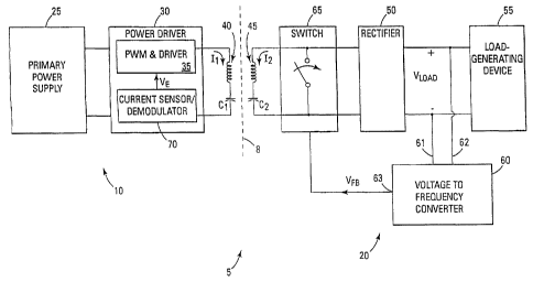
FIG. 1 is a block diagram of an embodiment of a medical
system in accordance with the invention.
FIG. 2 is a diagram, partially a block diagram and
partially a schematic diagram, of an embodiment of an
implantable apparatus that may be used in the medical system
shown in FIG. 1.
9
CA 02817934 2015-06-08
FIG. 3 is a block diagram of an embodiment of an
external apparatus that may be used in the medical system
shown in FIG. 1.
FIG 4 is a diagram, partially a block diagram and
partially a schematic diagram, of circuitry that may be used
in various embodiments of the external apparatus of FIG. 3.
Like reference symbols in the various drawings indicate
like elements.
DETAILED DESCRIPTION
A medical system 5 in accordance with the invention,
shown in FIG. 1, includes an external power supply apparatus
9a
CA 02817934 2013-05-28
that supplies power to an implanted apparatus 20, and
specifically to a load-generating device 55, such as a blood
pump, which is part of the implanted apparatus 20. The
external apparatus 10 has a primary coil 40 that may be
5 positioned adjacent to a secondary coil 45 in the implanted
apparatus 20 so that energy transfer occurs transcutaneously
through the patient's skin 8. The implanted apparatus 20
provides a feedback signal to the external apparatus 10 via
the same secondary coil 45 and primary coil 40 over which
10 energy transfer to the implanted apparatus 20 occurs. The
external apparatus 10 uses the feedback signal to control
the amount of energy transferred to the implanted apparatus
and thus regulate the load voltage (VI,oml) at device 55.
This control accommodates, for example, load variations with
15 device 55 and changes in energy transfer efficiency caused
by changes in the efficiency of the magnetic coupling
between the primary coil 40 and the secondary coil 45.
The external apparatus 10 includes a primary power
supply 25. The power supply 25 may include a DC battery to
20 produce the DC signal, may receive an AC signal from a power
line and rectify the signal to produce the DC signal, or may
have both a DC battery and the capability of receiving an AC
signal from a power line. The power supply 25 in one
implementation provides a DC signal to a power driver 30, as
is conventional. In this implementation, power driver 30
contains a conventional pulse-width modulator (PWM) and
driver 35 that conventionally produces a power signal having
an output voltage with a variable duty cycle and fixed
=
frequency, for example 160 kilohertz. The duty cycle of the
power signal's output voltage is dictated by an error signal
VE, which will be described later.
CA 02817934 2013-05-28
The power signal has a current I. that flows through
primary coil 40 and capacitor Cl. The primary coil 40 and
capacitor Cl form a conventional LC tank circuit. The LC
tank circuit is a resonant circuit whose resonant frequency
is set by the inductance of the primary coil 40 and the
capacitance of the capacitor Cl. In an example where the
resonant frequency of the LC tank circuit is equal to the
frequency of the power signal, current 11 is generally in
the shape of a sine wave.
1() Primary coil 40 is positioned next to the patient's
skin 8 and aligned with the secondary coil 45 located just
under the patient's skin 8 so that the primary coil 40 and
the secondary coil 45 become magnetically coupled. The
time-varying current I flowing through the primary coil 40
induces a corresponding time-varying current 12 that flows
through the secondary coil 45 and capacitor C2. The
secondary coil 45 and capacitor 02 form an LC tank circuit
similar to the primary coil 40 and the capacitor Cl on the
external apparatus 10. A rectifier 50 receives current 12
when normally open switch 65 is open and provides a DC
source of power for the load-generating device 55.
To regulate the load voltage (V1,0A0 at the load-
generating device 55, the implanted apparatus 20
communicates a feedback signal back to the external
apparatus 10 indicating the level of Vugm. As discussed
previously, Vvap may fluctuate or drop, for example, when
device 55 is drawing more current, or when the positioning
of primary coil 40 relative to the secondary coil 45 changes
= slightly thus causing a change in coupling efficiency. A
voltage-to-frequency (V-F) converter 60 has two inputs 61
and 62 connected across VLoAD to monitor the level of Vum.
11
CA 02817934 2013-05-28
The V-F converter 60 produces, at its output 63, a feedback
signal (Vp2) indicative of the level of VLOAD-
In this implementation, the feedback signal VFB is a
stream of brief pulses, the frequency of which varies with
variations in V. For example, a higher VLom, level may
result in the stream of pulses in the feedback signal Vri3
being generated at a lower frequency, whereas a lower VIA=
results in the stream of pulses in the feedback signal VF8
being generated at a higher frequency. The frequency of
pulses in the feedback signal VFB may be centered on a
specific center frequency, such as one kilohertz in one
implementation, which indicates no adjustment to the load
voltage VIA= is necessary. The frequency of pulses may
range, for example, from .8 kilohertz to 1.3 kilohertz. The
range of frequencies will typically be lower than the
frequency of time-varying currents 11 and 12 flowing through
coils 40 and 45, for reasons that will become apparent
later.
The V-F converter 60 provides the feedback signal ATFB
to the normally open switch 65. Each pulse of the feedback
signal VFB causes the switch 65 to close for the duration of
the pulse. Closing the switch 65 thus short-circuits the LC
tank circuit of secondary coil 45 and capacitor Cl, or in
other words, the end nodes of the series combination of
secondary coil 45 and capacitor 02 are connected to a common
node. This short-circuiting of the LC tank circuit causes a
pulse in current 12 to be generated across the secondary
coil 45. Because of the coupling between coils 45 and 40,
the current I in the primary coil 40 is related to the
voltage in the secondary coil 45. Reducing the voltage in
the secondary coil 45 by shorting the LC tank circuit causes
12
CA 02817934 2013-05-28
the current I. in the primary coil to reduce. Thus, the
pulse generated in the secondary coil 45 induces a
corresponding pulse in current I]. across the primary coil
40. As such, the feedback information contained in the
feedback signal VF8 is transferred from the implanted
apparatus 20 to the external apparatus 10 over the same
coils 40 and 45 over which power is transferred from the
external apparatus 10 to the implanted apparatus 20.
In the external apparatus 10, current
sensor/demodulator 70 senses the current I in the primary
coil 40. Current II contains two components: 1) the power
signal produced by the PWM and driver 35, and 2) the
feedback pulses caused by the closing of switch 65 in
response to the feedback signal VER. The current
sensor/demodulator 70 extracts the feedback pulses from the
current I. The current sensor/demodulator 70 also
processes the feedback pulses and generates an error signal
VE that is provided to the PWM and driver 35. The error
signal VE may be a signal whose voltage level goes lower as
the load voltage VLoAD needs to be reduced, and goes higher
as the load voltage Vmmr) needs to be increased. Based on
the error signal VE, the PWM and driver 35 changes the duty
cycle of the power signal it produces, thus altering the
amount of energy transferred to the implanted apparatus 20.
For example, if the error signal VE indicates that Vim') is
too low, the duty cycle of the power signal generated by the
PWM and driver 35 is increased to increase the amount of
energy transfer and thus raise the level of VLOAD-
Conversely, if VLOAD is too high, the duty cycle of the power
signal is decreased to lower the level of VLoAD. By changing
the duty cycle of the power signal produced by PWM and
13
CA 02817934 2013-05-28
driver 35, VLOAD is adjusted to remain within a specified
operating range.
FIG. 2 shows details of an embodiment of the implanted
apparatus 20 shown in FIG. 1. The function of the rectifier
50 shown in FIG. 1 is performed, in FIG. 2, by Zener diodes
102 and 104 and metal-oxide semiconductor field-effect
transistors (MOSFETs) 106 and 108. When the coil current 12
is positive, for example, current flows through diode 102 to
the positive terminal (+) of the load-generating device 55,
but does not flow to the negative terminal (-) because
MOSFET 106 is off. The current return path from the
negative terminal (-) is through MOSFET 108, which is
possible because the positive coil current 12 raises the
level of voltage at an input to driver 112 to MOSFET 108,
and thus MOSFET 108 is on. When current 12 is negative,
current flows through diode 104 to the positive terminal
(+), but not to the negative terminal (-) because MOSFET 108
is off. The current return path from the negative terminal
(-) is through MOSFET 106, which is possible because the
negative coil current 12 raises the level of voltage at an
input to driver 110 to MOSFET 106, and thus MOSFET 106 is
on. As such, the time-varying current 12 is rectified to
produce a DC power source to the medical device 55.
To monitor the load voltage VLot,D, the V-F converter 60
in this implementation includes a conventional error
amplifier 66. The error amplifier 66 measures the
difference between VLoAD and a reference voltage, and
provides, to a programmed microcontroller 64, a difference
signal VD/FF corresponding to the difference between IrLopn and
the reference voltage. In an example where load-generating
device 55 has a target VUAD of fourteen volts, the
14
CA 02817934 2013-05-28
a k
difference signal VDIET, after being scaled and shifted, may
range from zero volts, for a low VLoAD such as ten volts, to
five volts, for a high VLoAD such as twenty volts. The
microcontroller 64 is programmed to process the received
difference signal VD/FF, which contains information regarding
the present level of the load voltage VDCAD, and in response
generate the previously described pulsed feedback signal
VFB, which also contains information regarding the present
level of the load voltage VLORD-
In FIG. 2, MOSFETs 106 and 108 operate as switches and
thereby perform the function of the switch 65 shown in FIG.
1. The feedback signal VFB is provided to drivers 110 and
112 via capacitor C3 and diode 114 (for driver 110), and
diode 116 (for driver 112). Capacitor 03 eliminates the DC
component of VFB and passes only the pulse signal. The
diodes 114 and 116 allow Vn to turn on the drivers 110 and
112, but prevent VFB from turning the drivers 110 and 112
off. Resistors R1 and R2 limit the voltage to drivers 110
and 112 while allowing VFB to override these voltages.
The drivers 110 and 112 drive, respectively, MOSFETs
106 and 108. Drivers 110 and 112 simultaneously turn on
when feedback signal VFB pulses high, which simultaneously
turns on MOSFETs 106 and 108. Simultaneously turning on
MOSFETs 106 and 108 short-circuits the LC tank circuit of
the secondary coil 45 and capacitor Cl for the duration that
the feedback signal VFB pulses high. In other words, the
end nodes of the series combination of coil 45 and capacitor
02 are both tied to common node 118. As mentioned
previously, the shorting of the secondary coil 45 causes
pulses in the current 12, which in turn induces current
pulses in the current I through the primary coil 40. As a
CA 02817934 2013-05-28
result, the feedback signal VF B is transferred from the
internal apparatus 20 to external apparatus 10 using the
same primary coil 40 and secondary coil 45 over which power
is transferred from the external apparatus 10 to the
internal apparatus 20.
As will be appreciated in the FIG. 2 implementation.
MOSFETs 106 and 108 serve a dual function, as part of the
rectifier 50 and also as the switch 65 that imposes the
feedback pulses on the coil 45. As such, the switch 65 is
implemented in a manner that complements the functioning of
the rectifier 50.
FIG. 3 shows details of an embodiment of the external
apparatus 10 shown in FIG. 1. A conventional current-
sensing coil 150 placed in series with the primary coil 40
senses the current I/ flowing through the primary coil 40.
The current II passing through the current-sensing coil 150
induces a voltage signal (VsENsE) proportional to the current
on the secondary sensing coil 152. Like current II, the
voltage signal VSENSt on the secondary sensing coil 152
contains two components: 1) the power signal produced by the
PWM and driver 35, and 2) the feedback pulses.
The voltage signal VsENsE is received by a
rectifier/filter 155. The rectifier/filter 155, firstly,
rectifies the voltage signal VSENSEr keeping only the
positive portion of the signal. Second, the rectifier/filter
155 filters the power signal component from VsENsE, leaving
only the feedback signal component. This may be
accomplished with a conventional low-pass filter, which may
require the frequencies of the feedback signal to be much
lower than the frequency of the power signal. For example,
in one implementation the power signal has a frequency of
16
CA 02817934 2013-05-28
160 kilohertz and the feedback signal has a center frequency
of one kilohertz. The resulting low frequency pulse signal
VR thus reproduces in the external apparatus 10 the feedback
signal VFB generated by the V-1- converter 60 in the
implanted apparatus 20.
The feedback decoder 165 receives the feedback signal
VR from the rectifier/filter 155. Recall, the frequency of
the feedback signal VEE is modulated with changes in the
load voltage (VLoAD) of the internal apparatus 20. The
feedback decoder 165 demodulates the pulse signal VR
creating an error signal VE whose voltage level corresponds
to the frequency of the feedback signal pulses.
In one implementation, the feedback decoder 165 first
amplifies and conditions the pulse signal VR received from
the rectifier/filter 155. Next, a controller in the
feedback decoder 165 receives the amplified and conditioned
pulse signal VR and generates a constant-frequency,
rectangular pulse signal whose duty cycle changes with
respect to the frequency of the pulses in VR. The
rectangular pulse generated by the controller is then
averaged by an integrator to produce the error signal V.
The feedback decoder 165 supplies the averaged signal VE to
the input of a PWM 180.
An auto tune circuit 115 monitors both the current
signal and the voltage signal in the primary coil 40 to
determine whether these signals have an ideal timing
relationship with respect to each other. An ideal timing
relationship may be necessary to prevent the undesirable
dissipation of power in the external apparatus 10. For
example, it may be ideal when the timing of the current
17
CA 02817934 2013-05-28
signal in the primary coil 40 is slightly delayed with
respect to the timing of the voltage signal.
In one implementation, the auto tune circuit 175
contains flip-flops that generate signals relating to the
timing relationship between the voltage and current on
primary coil 40. For example, a first flip-flop may
generate a signal at the moment the current signal in the
primary coil 40 changes polarity, i.e., the current signal
crosses from negative to positive or from positive to
negative. Similarly, a second flip-flop may generate a
signal as the voltage signal in the primary coil 40 changes
polarity. The output of these flip-flops may then be summed
and compared to a fixed reference. If the voltage and
current signals do not have an ideal timing relationship,
the comparator may generate a tuning signal to be received
by the PWM 180. Upon receiving this tuning signal, the PWM
180 may adjust the frequency of the signal it produces
thereby achieving an ideal timing relationship between the
voltage and current signals in the primary coil 40.
The PWM 180 may be any conventional PWM known in the
art, or later developed. In one implementation, the PWM 180
receives the error signal VE from the feedback decoder 165
and generates a rectangular pulse signal (Vpm) which is sent
to a PWM driver 185. The duty cycle of the PWM output
signal Vpiqm varies according to V. By varying the duty cycle
of the PWM 180 output signal (Vm), the external apparatus
10 controls the amount of energy transferred to the internal
apparatus 20. In one example, a duty cycle for Vpi,m of 50%
results in the highest drive current I on the primary coil
40. If the error signal VE indicates that Vump is below an
optimal level, the duty cycle of the signal generated by the
1
1
CA 02817934 2013-05-28
PWM 180 may be adjusted up to 50%, thereby increasing the
amount of energy being transferred to the internal apparatus
20. Similarly, if the error signal Vt indicates that VLOAD
is above an optimal level, the duty cycle of the signal
generated by the PWM 180 may be decreased from 50% to zero.
By continuously changing the duty cycle of the signal Vpwm
produced by the PWM 180, VLOAD may be adjusted to remain
within a specified operating range.
The PWM driver 185 may be any conventional driver known
in the art, or later developed. The driver 185 receives the
output signal Vpwm of the PWM 180 and boosts the level of the
current in the output signal. The driver 185 applies the
output signal to the LC tank circuit of primary coil 40 and
capacitor Cl.
In summary, when the load voltage VLOAD raises, the
frequency of pulses in the pulsed feedback signal VFB is
lowered. As such, the error voltage VE is lowered, which
reduces the duty cycle of the PWM output signal Vpm and the
energy being transferred to the implanted apparatus 20.
Conversely, when the load voltage VmAD lowers, the frequency
of pulses in the pulsed feedback signal VFB is raised, as is
the error voltage VE. This raises the duty cycle of the PWM
output signal Vpm and consequently the energy being
transferred to the implanted apparatus 20. As such, the
load voltage VLOAD may be maintained to be within a desired
range.
FIG. 4 shows example circuitry that may be included in
an external power supply apparatus 10. The rectifier/filter
155 includes a rectifier 190 that receives the sensed
voltage signal VSENSE. The rectified sensed voltage signal
is forwarded to a low pass filter 192, which, as discussed
19
CA 02817934 2013-05-28
=
previously, eliminates the power signal component of the
VsENEE signal. The filtered and rectified pulse signal VR is
then forwarded to the feedback decoder 165, and in
particular, a micro-controller 194 in the decoder 165. The
micro-controller 194, in one implementation, is programmed
to produce another pulsed signal Vmc whose frequency is
constant, but whose duty cycle corresponds to the frequency
of pulses in the rectified and filtered pulsed signal VII. In
other words, when the frequency of pulses in the pulsed
signal VR goes lower, the duty cycle of the signal VC is
reduced. The micro-controllers output signal Vmc is sent to
an integrator 196. The integrator 196, in one embodiment,
averages the signal Vmc over time and produces an output
signal VE which has a voltage level that corresponds to the
average voltage level of VN: received over a particular
period of time. Thus, if the duty cycle of the signal limc
goes higher, then the error signal VE would likewise go
higher.
In some cases, the responsiveness of the feedback
system will be acceptable using only the information in the
feedback signals (and thus only the microcontroller output
signal Vmc). In other cases, more responsiveness may be
desired. The current I flowing through primary coil 40 is
affected by load current going to device 55, coupling of
coils 40 and 45, etc. As such, the magnitude of the primary
current I may not be trusted as a source of feedback
information.
However, the rate of change in the primary current
mirrors the rate of change of the load voltage Vump. For
example, with a faster increase of the load voltage \lump,
the primary current I is increasing faster. As such, it is
CA 02817934 2013-05-28
possible to use the differential of the primary current
(that is, rate of Change) as a contributing factor in the
feedback control loop.
To achieve this higher responsiveness, a resistor-
capacitor (R-C) circuit 198 may be added and connected to
the output of rectifier 190 as shown in FIG. 4. The R-C
circuit 198 receives the rectified voltage signal from
rectifier 190, and the voltage V2 gradually increases when
the rate of change in primary current I. becomes greater.
In this implementation, the integrator 196 receives, in
addition to the signal Vmc from the micro-controller 194,
another signal labeled V2 from the R-C circuit 198. The
integrator 196 adds both inputs Vila and V2 and produces an
error signal Vg that takes into account both the frequency
of feedback pulses in signal VR (and thus the duty cycle of
Vt.%) and the rate of change in 12 that may be occurring. As
such, the responsiveness of the feedback may be increased
beyond what the frequency of feedback pulses would otherwise
allow.
A number of embodiments of the invention have been
described. For example, information other than load voltage
VLOAD may be transmitted from an implanted apparatus to an
external apparatus using pulses superimposed on the
secondary coil 45 (see FIG. 2). For example, other
information that may be transmitted may include telemetry or
other logic information such as, in the case of a blood pump
being the load-generating device, an indication that the
pump is operating properly or is in fault, that an internal
battery is fully charged or not, or whether the pump is
operating on main or redundant components. Where
information such as this is being transmitted, a coding
21
CA 02817934 2013-05-28
scheme may be used so that different recognizable pulse
sequences correspond to different conditions, and thus the
external apparatus will be able to ascertain the condition
being transmitted. The coding scheme may also include a
pulse sequence that serves as a "start bit,' to inform the
external apparatus that the pulses that follow is condition
information. A microcontroller or other circuitry may be
included in the implantable apparatus (similar to the
microcontroller 64 shown in FIG. 2), which receives
information about sensed conditions, and produces the pulses
corresponding to the conditions. Therefore, it will be
understood that various modifications may be made without
departing from the spirit and scope of the invention.
Accordingly, other embodiments are within the scope of the
following claims.
25
22