Note: Descriptions are shown in the official language in which they were submitted.
CA 02817966 2013-05-14
WO 2012/068221
PCT/US2011/060942
SYSTEMS, METHODS AND/OR DEVICES FOR PROVIDING LED LIGHTING
CROSS-REFERENCE TO RELATED APPLICATIONS
[0001] This application claims priority to U.S. Provisional Application
No.
61/413,995, filed on November 16, 2010 and U.S. Provisional Application No.
61/532,104, filed September 8, 2011. This application is also related to PCT
Application No. PCT/ __ / _______ , entitled "Systems, Methods and/or
Apparatus for Thermoelectric Energy Generation," filed on November 16, 2011.
Each of these applications are herein incorporated by reference in their
entirety.
FIELD
[0002] This disclosure generally relates to systems, methods, and devices for
providing LED lighting. This disclosure also relates to systems, methods, and
devices for providing LED lighting with reduced energy consumption.
BACKGROUND
[0003] LED lighting has come to the forefront as a more efficient means of
providing household and commercial lighting. In contrast to most conventional
lighting techniques, LEDs generally require electrical flow in one direction
or direct
current ("DC") in order to produce light. Since standard building wiring
throughout the
world is alternating current ("AC"), LED lighting designs typically take one
of two
prevailing approaches to insure sustainable light.
[0004] The first approach utilizes a driver circuit that converts AC to DC,
steps down, and conditions the power. A typical converter design currently in
the
market utilizes up to eighty components to achieve the conversion and may use
additional components if dimming is required. The second approach is to use AC
LED technology.
[0005] These systems can be complex and inefficient because much of the
energy is emitted as heat and the system does not manage the heat loss
effectively.
Additionally, there are inefficiencies caused by interference from within the
system.
[0006] Accordingly, it would be desirable to have a system that managed the
emitted heat in a more effective manner and reduced the inefficiencies caused
by
interference from within the system.
-1-
CA 02817966 2013-05-14
WO 2012/068221
PCT/US2011/060942
SUMMARY
[0007] In exemplary embodiments of LED lighting systems, methods, and
devices, the LEDs may be isolated or substantially isolated from each other to
avoid
or reduce optical, thermal, and/or electrical interference associated with the
production of visible light.
[0008] Exemplary embodiments may provide a method for blocking the
adverse effects on LEDs of light produced by adjacent LEDs in LED arrays. For
example. when light from one LED (the first LED) hits another LED (the second
LED)
there may be at least two different things that negatively affect the ability
of the
second LED to produce light. First, the reflected light creates a voltage in
the second
LED (i.e., electrical interference) which negatively affects the ability of
the second
LED to produce photons. Second, the light emitted by the first LED reflects
off the
lens covering the second LED (i.e., optical interference) reducing the ability
of the
second LED to emit it's own light producing photons.
[0009] In exemplary embodiments, a lens between the LEDs may be utilized
to block the path of light from one LED to another LED. These lenses or
shields
reduce and/or eliminate at least one or both of the electrical and optical
interference
of the first LED on the second LED.
[0010] In exemplary embodiments, active heat management may be
implemented using a thermoelectric device(s) that convert heat generated by
the
LEDs or other components (including, e.g., the sun) into electrical energy
that is used
to cool the LEDs.
[0011] In exemplary embodiments, thermoelectric generators adjacent to the
LEDs and/or transformers may be used to convert the emitted heat into
electrical
energy. In exemplary embodiments, the electrical energy may be used to power a
thermoelectric device(s) that actively cools the LEDs. In exemplary
embodiments,
this approach may be advantageous to typical passive aluminum heat sinks since
the
heat sink simply removes the heat but is unable to utilize it for any purpose.
[0012] In exemplary embodiments, a pair of AC powered LEDs with opposite
polarity may be used to produce constant light. In exemplary embodiments, the
paired LEDs when positioned in close proximity to each other produce a steady
stream of light without a noticeable strobe effect notwithstanding that each
LED is
cycling at e.g., between 50-60 pulses per second.
[0013] In exemplary embodiments, power control at the component level may
be utilized to minimize and/or reduce power consumption and optimize and/or
-2-
CA 02817966 2013-05-14
WO 2012/068221
PCT/US2011/060942
improve performance. By properly sizing components to draw just the power that
is
needed for the application, exemplary embodiments may reduce and/or minimize
the
amount of power that is drawn and dissipated as heat. In exemplary
embodiments,
the device and/or system may utilize only a few components to produce light
from the
LEDs. For example, in exemplary embodiments, the main component may be a step
transformer that may be governed by two resistors. In exemplary embodiments,
there
may be no special driver board or dimmer boards required in any application.
Additionally, in exemplary embodiments, the active heat management system may
have no outside power consumption as it may be powered by wasted energy and
may be on an entirety isolated circuit.
[0014] In exemplary embodiments the LED lighting may not require the
conversion of power from AC to DC or the storage of current as used by current
systems, each of which results in loss of energy. Thus in exemplary
embodiments,
the LED lighting may:
= eliminate and/or reduce the need for costly driver circuitry used by
current systems to convert power from AC to DC;
= eliminate and/or reduce the need for capacitor circuitry used by
current systems to store power for use in off cycles;
= eliminate and/or reduce the need for special circuitry used by current
systems to allow for dimming. In exemplary embodiments, a standard
dimmer may be used to dim the LED lighting;
= be more reliable than previous systems;
= manage heat more effectively;
= extended the life of the LEDs since each LED is only powered half of
the time of operation, in effect, doubling, or substantially doubling its
life;
= eliminate, or at least reduce, the use of circuit boards for more
effective thermal management.
= eliminate, or at least reduce, the use of the reflow process to
minimize, or at least reduce, damage to the LED in the fixture
manufacturing process; and
= reduce the number of types of components for the LED lighting device
to just the LED.
[0015] In exemplary embodiments, the life of the LED may be extended
because of any combination of the following: (1) half operation of the LEDs as
discussed in exemplary double string A/C embodiments; (2) reducing the current
-3-
CA 02817966 2013-05-14
WO 2012/068221
PCT/US2011/060942
through each LED by using more LEDs per fixture; (3) maintaining the LEDs in a
cooler operating and ambient temperature; (4) not subjecting the LEDs to the
high
temperatures of a reflow process often used in populating circuit boards; (5)
eliminating, or at least reducing, the printed circuit board primarily used
for LED
lighting and utilizing a substrate that eliminates, or at least reduces,
thermal build up
around the LEDs; and/or (6) eliminating, or at least reducing, the printed
circuit board
primarily used for LED lighting and utilizing the substrate that is part of a
system to
harvest the unwanted LED thermal energy.
[0016] Exemplary embodiments may provide a lighting device comprising: a
plurality of LEDs; a plurality of optic devices corresponding to the plurality
of LEDs; at
least one optical separator for substantially preventing the light emitted
from one LED
from effecting the other LEDs; a thermoelectric device configured to harvest
heat
generated by the LEDs and convert the harvested heat into electrical energy;
and a
low temperature material for creating a temperature difference across the
thermoelectric device.
[0017] In exemplary embodiments of the lighting device at least one optical
separator substantially prevents a change in refractive index of the other
lights.
[0018] In exemplary embodiments of the lighting device at least one optical
separator substantially prevents a photovoltaic effect on the other lights.
[0019] In exemplary embodiments of the lighting device the low temperature
material is a phase change material.
[0020] In exemplary embodiments of the lighting device the generated
electrical energy is used to aid in maintaining the low temperature material
at a low
temperature.
[0021] In exemplary embodiments of the lighting device the generated
electrical energy is used to aid in powering at least one additional LED.
[0022] In exemplary embodiments of the lighting device the lighting device is
supplied with DC voltage.
[0023] In exemplary embodiments, the DC power may be harvested from the
site where the light is needed, e.g., waste thermal energy from a water line
or other
local process, radio waves, sunlight, etc.
[0024] In exemplary embodiments of the lighting device the lighting device is
supplied with AC voltage and at plurality of LEDs are arranged such that about
50%
are in a first polarity and about 50% are in a reverse polarity.
[0025] Exemplary embodiments may provide a lighting device comprising: a
plurality of lighting means for providing light; a plurality of optic means
corresponding
-4-
CA 02817966 2013-05-14
WO 2012/068221
PCT/US2011/060942
to the plurality of lighting means; at least one optical separator means for
substantially preventing the light emitted from one lighting means from
effecting the
other lighting means; thermoelectric means configured to harvest heat
generated by
the lighting means and convert the harvested heat into electrical energy; and
a low
temperature means for creating a temperature difference across the
thermoelectric
device.
[0026] In exemplary embodiments, the lighting means may be LEDs.
[0027] In exemplary embodiments of the lighting device at least one optical
separator means substantially prevents a change in refractive index of the
other
lights.
[0028] In exemplary embodiments of the lighting device at least one optical
separator means for substantially preventing a photovoltaic effect on the
other lights
may be provided.
[0029] In exemplary embodiments of the lighting device the low temperature
means is a phase change material.
[0030] In exemplary embodiments of the lighting device the generated
electrical energy is used to aid in maintaining the low temperature means for
storing
thermal energy at a low temperature.
[0031] In exemplary embodiments of the lighting device the generated
electrical energy is used to aid in powering at least one additional lighting
means.
[0032] In exemplary embodiments of the lighting device the generated
electrical energy may be used to aid in powering a device not associated with
the
lighting device but able to be powered by the generated energy e.g., smoke
detectors, motion detectors, cameras, etc.
[0033] In exemplary embodiments of the lighting device the generated
electrical energy may be used to aid in powering a device associated with the
lighting
device that is able to be powered by the generated energy e.g., timers,
controllers,
servos, etc.
[0034] In exemplary embodiments of the lighting device the lighting device is
supplied with DC voltage.
[0035] In exemplary embodiments, the DC power may be harvested from the
site where the light is needed, e.g., waste thermal energy from a water line
or other
local process, radio waves, sunlight, etc.
[0036] In exemplary embodiments of the lighting device the lighting device is
supplied with AC voltage and at plurality of lighting means are arranged such
that
about 50% are in a first polarity and about 50% are in a reverse polarity
-5-
CA 02817966 2013-05-14
WO 2012/068221
PCT/US2011/060942
[0037] In exemplary embodiments of the lighting device the lighting device
may be supplied with AC voltage and at plurality of LED means are arranged
such
that about 50% are in a first polarity and about 50% are in a reverse polarity
and the
voltage is stepped up or down by use of a transformer with governing
resistance.
[0038] In exemplary embodiments of the lighting device the lighting device
may be supplied with AC voltage where the number of LEDs placed in series
equals
the A/C input voltage to reduce (or substantially eliminate) the efficiency
loss of a
transformer.
[0039] In exemplary embodiments of the lighting device the lighting device
may be supplied with AC voltage and at plurality of LEDs means are arranged
such
that about 50% are in a first polarity and about 50% are in a reverse polarity
and the
lighting device is supplied with AC voltage where the forward voltage of the
LED's
placed in series match the supplied AC voltage to eliminate the efficiency
loss of a
transformer.
[0040] In exemplary embodiments of the lighting device the lighting device
may be supplied with AC voltage and the first four LEDs are configured as
diodes in
a typical rectifying pattern where the reverse current allowable for the LEDs
is not
exceeded giving the remaining LED DC power and the forward voltage of the
LED's
placed in series matching the supplied AC voltage.
[0041] In exemplary embodiments of the lighting device the lighting device
may be supplied with AC voltage and the first four LEDs are configured as
diodes in
a typical rectifying pattern where the reverse current allowable for the LEDs
is not
exceeded giving the remaining LED DC power and the voltage is stepped up or
down
by use of a transformer with governing resistance.
DESCRIPTION OF THE DRAWINGS
[0042] Exemplary embodiments will now be described, by way of example
only, with reference to the accompanying drawings in which:
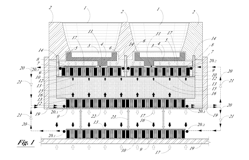
[0043] FIG. 1 is a schematic diagram of an exemplary LED lighting device;
[0044] FIG. 2 is a schematic diagram of an exemplary LED lighting device;
[0045] FIG. 3 is a schematic diagram of an exemplary LED lighting device;
[0046] FIG. 4 is a schematic diagram of an exemplary LED lighting device;
[0047] FIG. 5 is a schematic diagram of an exemplary transformer assembly
for use in an LED lighting assembly;
[0048] FIG. 6 is a schematic diagram of an exemplary AC LED assembly;
-6-
CA 02817966 2013-05-14
WO 2012/068221
PCT/US2011/060942
[0049] FIG. 7 is a schematic diagram of an exemplary LED mounting
structure for use in an LED lighting assembly where a thermal path is made
using
substantially solid vias;
[0050] FIG. 8 is a schematic diagram of an exemplary active heat
management system for use in an LED lighting assembly;
[0051] FIG. 9 is a schematic diagram of an exemplary DC circuit for use in an
LED lighting assembly for harvesting thermal energy from four local heat
sources,
converting the thermal energy to electrical energy using thermoelectric
generators (in
series), to power a thermoelectric chiller;
[0052] FIG. 10 is a schematic diagram of an exemplary DC circuit for
harvesting thermal energy from one local heat source in an LED lighting
assembly
and converting the thermal energy to electrical energy using a thermoelectric
generator to power a thermoelectric chiller;
[0053] FIG. 11 is a schematic diagram of an exemplary DC circuit for
harvesting thermal energy from two local heat sources in an LED lighting
assembly
and converting the thermal energy to electrical energy using two
thermoelectric
generators, in parallel, to power a thermoelectric chiller;
[0054] FIG. 12 is a schematic diagram of an exemplary DC circuit for
harvesting thermal energy from two local heat sources in an LED lighting
assembly
and converting the thermal energy to electrical energy using two
thermoelectric
generators, in series, to power a thermoelectric chiller;
[0055] FIG. 13 is a schematic diagram of an exemplary DC circuit for
harvesting thermal energy from one local heat source in an LED lighting
assembly
and converting the thermal energy to electrical energy using a thermoelectric
generator to power another local device, e.g., a camera, a timer or a sensor
etc;
[0056] FIG. 14 is a schematic diagram of an exemplary DC circuit for
harvesting thermal energy from two local heat sources in an LED lighting
assembly
and converting the thermal energy to electrical energy using two
thermoelectric
generators, in parallel, to power another local device, e.g., a camera, a
timer or a
sensor, etc;
[0057] FIG. 15 is a schematic diagram of an exemplary DC circuit for
harvesting thermal energy from two local heat sources in an LED lighting
assembly
and converting the thermal energy to electrical energy using two
thermoelectric
generators, in series, to power another local device, e.g., a camera, a timer
or a
sensor;
-7-
CA 02817966 2013-05-14
WO 2012/068221
PCT/US2011/060942
[0058] FIG. 16 is a schematic diagram of an exemplary embodiment of an
electromagnetic and thermal energy harvesting power supply for use in e.g., an
LED
lighting assembly;
[0059] FIG. 17 is a schematic diagram of an exemplary embodiment of cross-
section A of the exemplary power supply of FIG. 16 for use in an LED lighting
assembly;
[0060] FIG. 18 is a schematic diagram of an exemplary embodiment of cross-
section B of the exemplary power supply of FIG. 16 for use in an LED lighting
assembly;
[0061] FIG. 19 is a schematic diagram of an exemplary embodiment of cross-
section C of the exemplary power supply of FIG. 16 for use in an LED lighting
assembly;
[0062] FIG. 20 is a schematic diagram of an exemplary AC LED assembly
which uses the first 4 LEDs in the string to rectify the AC power without
requiring the
use of additional components;
[0063] FIG. 21 is a schematic diagram of an exemplary embodiment of an
LED lighting assembly; and
[0064] FIG. 22 is a schematic diagram of an exemplary embodiment of an
LED lighting assembly for use in e.g., a refrigerator room/case.
DESCRIPTION OF EXEMPLARY EMBODIMENTS
[0065] LED lighting is a more efficient way of providing lighting in a variety
of
situations. The technology is also greener and often more cost effective than
conventional lighting. As would be understood by a person of ordinary skill in
the art,
LED lighting uses less energy to produce comparable quantities of light
thereby
reducing the amount of energy being consumed, LEDs also generally last longer
than
conventional lighting thereby reducing the frequency of replacement. However,
there
are still some inefficiencies with LED lighting. Some of these inefficiencies
(i.e., heat
generation) are a result of the LED itself but others are the result of the
system
design. By reducing at least one of these inefficiencies, the LED lighting can
be even
more useful.
[0066] of providing household and commercial lighting. In contrast to most
conventional lighting techniques, LEDs generally require electrical flow in
one
direction or direct current ("DC") in order to produce light. Since standard
building
wiring throughout the world is alternating current ("AC"), LED lighting
designs
typically take one of two prevailing approaches to insure sustainable light.
-8-
CA 02817966 2013-05-14
WO 2012/068221
PCT/US2011/060942
[0067]
[0068] FIG. 1 is a schematic diagram of an exemplary LED lighting device. In
FIG. 1, an individual optic device 1 is used for each LED in the exemplary
fixture. An
optic separator 2 may be set at the edge of the LED lens 3 and may be a part
of or
be separate from the optic device 1. This arrangement may help to ensure that
substantially less, little to no stray light from the other LEDs or elsewhere
cause a
reflection across the protected LED thus changing its refractive index or
otherwise
causing an unwanted photovoltaic effect on the semiconductor at the base of
the
LED lens 3. As shown in FIG. 1, the LED lens 3 may be seated in an LED die 4.
In
exemplary embodiments, the LED anode 5 and LED cathode 6 may be connected to
the fixture circuit layer 7 using electrically and thermally conductive epoxy
8 that may
cure at a temperature below 70 C, to avoid high temperatures (e.g., >260 C )
typically
used by the electronics industry in reflow ovens. As would be understood by
persons
of ordinary skill in the art, the oven temperatures may be more than those
considered
safe for LEDs. Exposure to these high temperatures causes loss in lifetime. In
exemplary embodiments, limiting the exposure of the LEDs to temperatures below
70 C (e.g., below 100 C, below 90 C, below 80 C, below 75 C, below 70 C, below
65 C, below 60 C, below 50 C, etc.) may extend the duty cycle of the LEDs.
[0069] In exemplary embodiments. the circuit layer 7 may be a
semiconductor device specific electrically conductive pad and trace layer
applied
directly to the thermally conductive, but electrically non-conductive,
thermoelectric
device substrate (hot side) 9 of a thermoelectric device 10. In exemplary
embodiments, this may be accomplished by way of printing, etching or
fastening, that
eliminates the use of circuit boards. The elimination of the circuit board may
achieve
two benefits; firstly, it may allow for a direct path of component thermal
waste energy
away from the component eliminating the common heat buildup into the circuit
board's dielectric layer that has negative effects on the components and
secondly, it
may make possible the use of a printed, etched or fastened trace to the
substrate as
a resistor eliminating circuit components.
[0070] The LED circuit begins and ends with LED power supply connectors
11 and in exemplary embodiment no driver board may be required as the circuit
layer
7 may be engineered to include the LED component specific current and voltage
resistance and/or impedance in the case of alternating current. The
thermoelectric
device substrate (cold side) 12 of the thermoelectric device 10 is fastened,
using
known methods practiced for thermoelectric devices, to a thermally conductive
substrate 13. The thermally conductive substrate 13 may include thermally
-9-
CA 02817966 2013-05-14
WO 2012/068221
PCT/US2011/060942
conductive vertical path walls 14 that attach to the optic separator 2 to
chill the
ambient temperature of the LEDs and may also be part of the containment
structure
for low temperature phase change material storage 15.
[0071] In operation, when electrical energy is connected to the circuit layer
7
by way of the LED power supply connectors 11, the connected LEDs emit light as
intended but also produce waste heat through the LED anode 5 and LED cathode
6.
The waste heat is drawn away through the thermoelectric device 10 towards the
low
temperature phase change material storage 15 in a calculable and definable
high
temperature flow direction 17. The design temperature of the low temperature
phase
change material storage 15, the low temperature flow direction 16, the thermal
energy produced by the LEDs, and the thermal resistivity of the thermoelectric
device
determines the amount of wasted heat energy converted back into electrical
energy. Parts of the low temperature phase change material storage 15 that is
not
desired to be thermally conductive may be constructed using a thermal
insulating
barrier 18 to aid in maintaining the temperature of the low temperature phase
change
material storage 15.
[0072] Another source of heat to create a high temperature flow direction 17
through the thermoelectric device 10 towards the low temperature phase change
material storage 15 and generate electrical energy is the fixture's outer
housing 19 -
especially in outdoor fixtures during daytime hours as long as there is a
thermally
conductive link 23 to the low temperature phase change material storage 15.
The
electricity generated by the processes described herein moves as a direct
current
flow 20 from the positive leads 20.1 of the thermoelectric device 10 through
protection diodes 21(designed to confine the flow in one direction) and onto
the
positive lead 20.1 of the thermoelectric chiller 22 which continually chills
the low
temperature phase change material storage 15 and out the negative lead 20.2
through protection diodes 21 and onto the negative lead 20.2 of the
thermoelectric
device 10, completing the circuit.
[0073] In exemplary embodiments, this electrical circuit may be substantially
separated or completely separate from the circuit powering the LEDs. In
exemplary
embodiments, the power supply for the LED circuit may be done without
secondary
circuits because of the current and voltage regulating circuit layer 7. In the
case of
DC power, which in exemplary embodiments may be desirable, the selection of
the
proper DC power source voltage and amperage per the LED manufacture's
specifications may be sufficient to what is required. In the case of AC power,
exemplary embodiments may employ the use of a transformer that converts the in-
-10-
CA 02817966 2013-05-14
WO 2012/068221
PCT/US2011/060942
coming voltage and amperage to the desired power source voltage and amperage
of
the LEDs per the LED manufacture's specifications Additionally, in exemplary
embodiments, the LED circuit may have equal LEDs set on the circuit layer 7 in
reverse polarity and set in close proximity to its opposite LED, so as to use
both
sides of the electrical wave pattern. The use of resistors on both leads of
the high
voltage portion of the transformer may be suggested to maintain a longer
transformer
life. A method of eliminating the transformer may be to use a large number of
LEDs
in series to match the high voltage in buildings and use the first four LEDs
to act as
blocking diodes in a rectifying circuit configuration. Two of the fourLEDs
would
alternate and the rest of the LEDs would get a direct current. To eliminate
flicker on
the four LEDs, in exemplary embodiments, the alternating pairs may be close to
one
another or cover the same area at the working surface the LED lighting is
intended
for.
[0074] In exemplary embodiments, the LED components prior to being used
in a lighting system may have an efficacy of 150 Im/w at 2.86V and 350mA with
a
25 C Ambient and Solder Junction Temperature and a Lifecycle of 100,000 hours
(lifecycle may be to 70% efficiency) as may be specified by LED manufacturers.
[0075] Typical industry fixtures may have one or more of the following
features:
= A driver board designed for 3V and 500mA (power mismatch and
current overdrive): -30 Im/w - Lifecycle loss 5%;
= Driver board loss (NC to D/C and rectifying-smoothing): -40 Im/w -
Lifecycle loss 0%;
= The light may be mounted on PCB using reflow oven (heat
damage to LED integrated optics): -2 Im/w - Lifecycle loss 18%;
= Thermal design of fixture may not remove/reduce ambient heat: -5
Im/w - Lifecycle loss 22%;
= The thermal design of the fixture may not remove/reduce solder
junction heat: -5 lm/w- Lifecycle loss 10%;
= Optical light spillover: - 12 Im/w - Lifecycle loss 5%.
[0076] As a result of these inefficiencies, typical lighting solutions may
have
one or more of the following limitations:
= The LED Efficacy may drop from 150 Im/w to 56 lm/w;
= The LED Lifecycle may drop from 100,000 hours to 40,000 hours
(manufactures generally do not give more than a 5 year warranty);
= Other drawbacks may include:
-11-
CA 02817966 2013-05-14
WO 2012/068221
PCT/US2011/060942
= Other components on driver board may fail sooner;
= Driver board may cause more heat due to more
components;
= Heat transfer methods may not work in fixture housings like
ceiling cans;
= Outdoor fixtures subject to hot and cold changes daily may
cause damage to PCB by expansion and contraction;
= More components and larger heat sinks cost more;
= Since most fixtures share optics in an array, a large
percentage, (sometimes as great as 80%) of the lumens
that are not lost from the above mentioned reasons, may
not hit the working surface the fixture is intended for.
[0077] Using the features of the exemplary embodiments described herein,
the LED lighting may have one or more of the following features:
= A power source design for about 2.78V and 80mA (e.g.,
substantial power match to LED specifications): +72.57 Im/w (e.g.,
20 lm/w, 30 Im/w , 40 lm/w, 50 lm/w, 60 lm/w, 70 lm/w, 75 lm/w,
80 lm/w, 90 lm/w, etc.) - Lifecycle gain 600% (e.g., 50%, 100%,
200%, 300%, 400%, 500%, 700%, 800%);
= The LEDs may be mounted on the TEG substrate using
conductive paste: +/- 0 Im/w - Lifecycle loss 0% (e.g., substantially
no lifecycle loss);
= An active thermal design of fixture to remove/reduce ambient heat:
+ 8 Im/w (e.g., 4 lm/w, 5 lm/w, 6, lm/w, 7 lm/w, 9 lm/w, 10 lm/w, 15
lm/w, etc.) - Lifecycle Gain 100% (e.g., 20%, 30%, 40%, 50%,
60%, 70%, 80%, 90%, 100%, 110%, 120%, 130%, 140%, 150%);
= An active thermal design of fixture to remove solder junction heat
to: + 5 Im/w (e.g., 4 lm/w, 5 lm/w, 6, lm/w, 7 lm/w, 9 lm/w, 10 lm/w,
15 lm/w, etc.) - Lifecycle Gain 100% (e.g., 20%, 30%, 40%, 50%,
60%, 70%, 80%, 90%, 100%, 110%, 120%, 130%, 140%, 150%);
= The harvested thermal energy may be converted back to light: + 6
Im/w (e.g., 4 lm/w, 5 lm/w, 6, lm/w, 7 lm/w, 9 lm/w, 10 lm/w, 15
lm/w, etc.) - Lifecycle Gain 0% (e.g., substantially no lifecycle
loss).
-12-
CA 02817966 2013-05-14
WO 2012/068221
PCT/US2011/060942
= Minimal optical loss from lens or reflectors: -3% Im/w - (e.g., 1
lm/w, 2 lm/w, 3 lm/w, 4 lm/w, 5 lm/w, 6 lm/w, 7 lm/w, etc.) -
Lifecycle Loss 0% (e.g., substantially no lifecycle loss)
[0078] As a result of one or more of these features, exemplary embodiments
may experience one or more of the following improvements:
= LED Efficacy: raised from 150 Im/w to 234.32 Im/w (e.g., an
improvement of 25%, 30%, 40%, 50%, 55%, 60%, 70%, 75%,
80%, 90%, 100%, etc.);
= LED Lifecycle: raised from 100,000 hours to 800,000 hours (e.g.,
150,000, 200,000, 250,000, 300,000, 350,000, 400,000, 450,000,
500,000, 550,000, 600,000, 650,000, 700,000, 750,000, 800,000,
850,000, 900,000, 1,000,000 hours, etc.) or a life cycle extension
of e.g., 100%, 200%, 300%, 400%, 500%, 600%, 700%, etc.;
= Other advantages may include one or more of the following::
= Few/no other components necessary;
= Ease of manufacture, smaller BOM;
= Heat transfer methods may work in a number of fixture
housings and environments;
= Outdoor fixtures may benefit from harvesting heat from the
sun cold thermal energies at night;
= Fewer components so my cost less;
= Optic design at individual LED level improves the
percentage of the lumens that reach the intended working
surface;
= It may be possible to harvest more thermal energy to run
another type of sub system, e.g., camera, signal, sensors,
etc.
[0079] FIG. 2 is a schematic diagram of an exemplary LED lighting device.
The embodiment illustrated in FIG. 2 is similar to the embodiment described
above
with respect to FIG. 1 except the cold side of the thermoelectric device is in
contact
with a thermally conductive outer housing 19. This arrangement assumes that
the
ambient temperature is lower than the temperature of the waste heat so the
thermoelectric device produces electrical energy. Of course, as would be
understood
by a person of skill in the art, the electrical energy generated could be used
for a of a
number of purposes, e.g., powering a camera, sensor, alarm, etc., or
combinations
thereof
-13-
CA 02817966 2013-05-14
WO 2012/068221
PCT/US2011/060942
[0080] FIG. 3 is a schematic diagram of an exemplary LED lighting device. In
this embodiment, much like the embodiment of FIG. 2, there is no phase change
material. However, in this case, there is also no thermoelectric device.
Accordingly,
the housing 19 acts in a known manner to dissipate heat from the LEDs. Of
course,
as would be understood by a person of ordinary skill in the art, this
embodiment may
still use the optics described herein. Additionally, as illustrated in this
exemplary
embodiment, the housing 19 includes "island" pads in the shape of the
substrates 13
for better heat isolation.
[0081] FIG. 4 is a schematic diagram of an exemplary LED lighting device.
This embodiment is similar to the embodiment of FIG. 3 except the outer
housing 19
includes sintered heat pipes 24 and working fluid 25. The heat pipes 24 and
working
fluid 25 aid in drawing away the waste heat from the LEDs.
[0082] FIG. 5 is a schematic diagram of an exemplary transformer assembly
for use in an LED lighting assembly. In exemplary embodiments, the LED
lighting
assembly may utilize a thermally isolated standard step-down power transformer
26
to more precisely match the input voltage and current to the LED manufacture's
specifications. The resistors 28 may be sized to limit the power drawn from
the
transformer 26 so as not to overheat the transformer and reduce it's lifespan.
The
waste thermal energy from the transformer 26 and Resistors 28 clamped against
a
Thermally Conductive Substrate 13 may also be harvested as shown in Fig. 8
[0083] FIG. 6 is a schematic diagram of an exemplary AC LED assembly. In
FIG. 6, two sets of LED strings 38 are wired with opposite polarity so that
they are
powered and produce light in an alternating fashion without the need for an
LED
driver circuit. Although in exemplary embodiments an LED driver circuit may be
used.
[0084] FIG. 7 is a schematic diagram of an exemplary LED mounting
structure for use in an LED lighting assembly. In FIG. 7, LEDs 29 with
opposite
polarity are mounted on a thermally modified printed circuit board or PCB 30
in pairs
so that a pair produces a steady stream of light. In exemplary embodiments,
opposing LEDs are spaced at a distance of no more than the diameter of their
isolating lens plus an additional distance for ease of manufacture, to prevent
or
reduce a possible strobe effect. Alternatively, in exemplary embodiments, the
lighting may be placed at other distances from each other so long as they are
aimed
at the same, or substantially the same, surface.
[0085] The thermal pads 30.1 upon which the LEDs are mounted are "I"
shaped, electrically isolated and have 0.25mm solid copper vias 30.2 spaced as
-14-
CA 02817966 2013-05-14
WO 2012/068221
PCT/US2011/060942
close together as PCB manufacturing will allow to an identical, or
substantially
similar, thermal pad on the backside of the PCB. This passive thermal
technique
helps transfer the heat from the LED 29 die solder junction to the back of the
PCB
30. LEDs 29 may be attached to the PCB 30 using the reflow method specified by
the LED manufacturer and/or an electrical and thermal conductive epoxy.
[0086] FIG. 8 is a schematic diagram of an AC LED lighting assembly with an
exemplary active heat management system for use in an LED lighting assembly.
The active heat management system draws away the passively transferred waste
heat at the backside of the PCB 30 and converts it into electrical energy. In
the
exemplary embodiment of FIG. 8, the PCB 30 may be mechanically attached to the
primary heat-sink plate 13 that is shaped to match the thermal pads 30.1 of
the LEDs
29 so as not to allow heat to dissipate across the backside of the PCB 30. The
thermal connection of the pad to plate is enhanced by the use of thermal
adhesive. In
exemplary embodiments, the transformer 26 may be mechanically attached to the
primary heat-sink plate 13 but isolated from the PCB 30 by dropping it below
the
Isolation Wall 18. The thermal connection of the Transformer 26 to plate is
enhanced
by the use of thermal adhesive.
[0087] In exemplary embodiments, the resistors 28 may be mechanically
attached to the primary heat-sink plate 13 using a resistor clamp 27 and is
also
sufficiently isolated from the PCB 30 by dropping it below the isolation wall
18. The
thermal connection of the resistors 28 and the resistor clamp 27 to plate is
enhanced
by the use of thermal adhesive.
[0088] In exemplary embodiments, a heat-sink stack of thermally conductive
substrate 13 matching the thermal pads 30.1 of the LEDs 29 may be attached by
compression to the primary thermally conductive substrate 13. The thermal
connection of the primary thermally conductive substrate 13 to stack is
enhanced by
the use of thermal adhesive.
[0089] In exemplary embodiments, an isolation wall 18 that houses
thermoelectric device 22 with their "hot side" facing the heat-sink stack 13
may be
attached by compression to the heat-sink stack 13. The thermal connection of
the
stack to the thermoelectric device 22 may be enhanced by the use of thermal
adhesive.
[0090] In exemplary embodiments, the thermoelectric device 10 may receive
most of the waste heat generated by the LEDs 29, the transformer 26 and the
resistors 28 as described herein and are configured in series, parallel or a
mix of both
to define the output to the desired configuration of the electrical power (
volts and
-15-
CA 02817966 2013-05-14
WO 2012/068221
PCT/US2011/060942
amps) they generate from the waste heat. These configurations of the
thermoelectric
devices 10 would be readily understood by a person of ordinary skill in the
art.
Additional thermoelectric devices may also be stacked behind the
thermoelectric
device 10 shown to transfer heat in stages to produce additional power and
move the
heat further from the PCB 30.
[0091] In exemplary embodiments, a phase change material packet ring 15
may be chilled by thermoelectric devices 22 that are powered by the reclaimed
energy from wasted heat to maximize the cooling. The thermoelectric devices 22
become thermoelectric chillers when DC power is applied in reverse polarity. A
blocking diode maintains the chilling effect by not allowing (or reducing the
likelihood)
the thermoelectric devices 22 to become thermoelectric heaters. The phase
change
material packet 15 material may have a target temperature of 20 C. In
exemplary
embodiments, this secondary DC power source would add substantially less,
little or
no additional power consumption for the LEDs, as it is reclaimed by energy
that
would typically go wasted. This configuration is illustrated in FIG. 9 which
is a
schematic diagram of an exemplary DC circuit for use in actively cooling an
LED
lighting assembly.
[0092] The lens used in most LED fixtures cause interference and diminish
the lumen output due to interference of the light generated by one LED with
the
ability of adjacent LEDs to operate at optimal efficiency ("LED to LED
interference").
In general, LED to LED interference comes in two forms. First, the reflection
of light
generated by one LED off the lens of another LED causes optical interference.
This
optical interference diminishes the efficiency of the LED luminary fixture.
Second, the
absorption of light generated by an LED by adjacent LEDs creates a small
photovoltaic effect resulting in a reverse voltage in the circuit interfering
with the
effectiveness of the power deployed to run the LED.
[0093] To mitigate the described interference, exemplary embodiments may
use individual lenses with isolation housing or reflectors to stop, or
substantially
reduce, the path of light from one LED to another and the negative effect
thereof. In
exemplary embodiments, the lenses may also tighten up the beam angle to the
desired spread. In exemplary embodiments, the desired spread may be determined
based on the entire array and not the individual LEDs.
[0094] In cases where a lens is utilized rather than a reflector an index
matched gel may also be utilized at the juncture point of the Lens and the LED
dome
to reduce loss caused by refraction at the juncture point. An exemplary
optical
adhesive is NOA 88. In general, the adhesive may have various combinations of
-16-
CA 02817966 2013-05-14
WO 2012/068221
PCT/US2011/060942
properties similar to one or more of those detailed below in Table 1:
Solids 100%
Viscosity at 25 C 200 cps (e.g., 200-5,000 cps, 500 cps, 1000 cps,
1000-2000 cps, 200-300 cps, 200-400 cps, 150-
250 cps, etc)
Refractive Index of 1.52 (e.g., 1.50, 1.51, 1.52, 1.53, 1.54 etc.)
Monomer
Refractive Index of Cured 1.56 (e.g., 1.51-1.58, 1.51, 1.52, 1.53, 1.54,
1.55,
Polymer 1.56, 1.57, 1.58, etc.)
Elongation at Failure 41% (e.g., 18-80%, 25%, 30%, 40%, 50%, 60%,
70%, 75%, etc.)
Modulus of Elasticity (psi) 131, 000(e.g., 131,000-150,000, 135,000,
140,000, 145,000, 150,000, etc.)
Tensile Strength (psi) 2,000 (e.g., 101-2800, 500, 750, 1000, 1250,
1500, 1750, 1900, 2100, 2500, 2700, 2800, etc.)
Hardness - Shore D 90 (e.g., 25-90, 25, 30, 40, 45, 50, 60, 70, 75,
80,
90, etc.)
Total Mass Loss (TML) 1.07%
Collected Volatile <0.01%
Condensable Material
(CVCM)
Dielectric Constant (1 4.06
MHz)
Dielectric Strength (V/mil) 457
Dissipation Factor (1 MHz) 0.0341
Volume Resistivity (ohm- 6.85 x 10¹⁴
cm)
Surface Resistivity 3.71 x 10¹²
(MEgohms)
Table 1: Exemplary Optical Adhesive Properties
[0095] FIG. 10 is a schematic diagram of an exemplary DC circuit for use in
actively cooling an LED lighting assembly. In FIG. 10, a single thermoelectric
generator 10 receives the wasted heat from a source, e.g., an LED, heat of the
sun
on the fixture case, etc. on one side described as the high temperature flow
17 and
receives a cooler temperature on its opposite side from a source, e.g. cooler
ambient
temperature, a low temperature phase change material or a condensation line,
etc.
described as a low temperature flow 16. The circuit generates direct current
electrical energy that flows through a blocking diode 21 placed as a
protection device
-17-
CA 02817966 2013-05-14
WO 2012/068221
PCT/US2011/060942
to ensure a single direction of electrical flow to a single thermoelectric
chiller 22. The
thermoelectric chiller 22 receives the electrical energy and pumps away heat
from
one side causing a low temperature flow 16 from one side and a high
temperature
flow 17 on the other. Another Blocking Diode 21 may be placed after the
thermoelectric chiller 22 before closing the circuit back at the
thermoelectric
generator 10.
[0096] FIG. 11 is a schematic diagram of an exemplary DC circuit for use in
actively cooling an LED lighting assembly. In FIG. 11, multiple thermoelectric
generators 10 receive the wasted heat from multiple sources, e.g., an LED,
heat of
the sun on the fixture case, etc. on one side described as the high
temperature flow
17 and receive cooler temperature on their opposite side from multiple
sources, e.g.
cooler ambient temperature, a low temperature phase change material or a
condensation line, etc. described as a low temperature flow 16. The circuit
generates multiple sources of direct current electrical energy connected
together in
parallel that flow through a blocking diode 21 placed as a protection device
to ensure
a single direction of electrical flow to a thermoelectric chiller 22 that
receives the
electrical energy and pumps away heat from one side causing a Low Temperature
Flow 16 from one side and a high temperature flow 17 on the other. Another
blocking diode 21 may be placed after the thermoelectric chiller 22 before
closing the
circuit back at the thermoelectric generators 10.
[0097] FIG. 12 is a schematic diagram of an exemplary DC circuit for use in
actively cooling an LED lighting assembly, where multiple thermoelectric
generators
receive the wasted heat from multiple sources, e.g., an led, heat of the sun
on the
fixture case, etc. on one side described as the high temperature flow 17 and
receive
cooler temperature on their opposite side from multiple sources, e.g. cooler
ambient
temperature, a low temperature phase change material or a condensation line,
etc.
described as a low temperature flow 16. The circuit generates multiple sources
of
direct current electrical energy connected together in series that flow
through a
blocking diode 21 placed as a protection device to ensure a single direction
of
electrical flow to a thermoelectric chiller 22 that receives the electrical
energy and
pumps away heat from one side causing a low temperature flow 16 from one side
and a high temperature flow 17 on the other. Another blocking diode 21 may be
placed after the thermoelectric chiller 22 before closing the circuit back at
the
thermoelectric generators 10.
[0098] FIG. 13 is a schematic diagram of an exemplary DC circuit for use in
actively cooling an LED lighting assembly and harvesting that thermal energy
and
-18-
CA 02817966 2013-05-14
WO 2012/068221
PCT/US2011/060942
converting it back into electrical energy. In FIG. 13, a single thermoelectric
generator
receives the wasted heat the LED or LEDs on one side described as the high
temperature flow 17 and receives a cooler temperature on the opposite side
from a
source, e.g. cooler ambient temperature, a low temperature phase change
material
or a condensation line, etc. described as a low temperature flow 16. The
circuit
generates direct current electrical energy that flows through a blocking diode
21
placed as a protection device to ensure a single direction of electrical flow
to any type
of electrical device capable of using the power provided shown as "work."
Another
blocking diode 21 may be placed after the thermoelectric chiller 22 before
closing the
circuit back at the thermoelectric generator 10.
[0099] FIG. 14 is a schematic diagram of an exemplary DC circuit for use in
actively cooling an LED lighting assembly and harvesting that thermal energy
and
converting it back into electrical energy. In FIG. 14, multiple thermoelectric
generators 10 receive the wasted heat from multiple sources, e.g., the LEDs,
heat of
the sun on the fixture case, etc. on one side described as the high
temperature flow
17 and receive cooler temperature on their opposite side from multiple
sources, e.g.
cooler ambient temperature, a low temperature phase change material or a
condensation line, etc. described as a low temperature flow 16. The circuit
generates multiple sources of direct current electrical energy connected
together in
parallel that flow through a blocking diode 21 placed as a protection device
to ensure
a single direction of electrical flow to various types of electrical devices
capable of
using the power provided shown as "work." Another blocking diode 21 may be
placed after the thermoelectric chiller 22 before closing the circuit back at
the
thermoelectric generator 10.
[00100] FIG. 15 is a schematic diagram of an exemplary DC circuit for use in
actively cooling an LED lighting assembly and harvesting that thermal energy
and
converting it back into electrical energy. In FIG. 15, multiple thermoelectric
generators 10 receive the wasted heat from multiple sources, e.g., the LEDs,
heat of
the sun on the fixture case, etc. on one side described as the high
temperature flow
17 and receive cooler temperature on their opposite side from multiple
sources, e.g.
cooler ambient temperature, a low temperature phase change material or a
condensation line, etc. described as a low temperature flow 16. The circuit
generates multiple sources of direct current electrical energy connected
together in
series that flow through a blocking diode 21 placed as a protection device to
ensure a
single direction of electrical flow to various types of electrical devices
capable of
using the power provided shown as "work." Another blocking diode 21 may be
-19-
CA 02817966 2013-05-14
WO 2012/068221
PCT/US2011/060942
placed after the thermoelectric chiller 22 before closing the circuit back at
the
thermoelectric generator 10.
[00101] FIG. 16 is a schematic diagram of an exemplary embodiment of an
electromagnetic and thermal energy harvesting power supply for use in e.g., an
LED
lighting assembly. FIG. 17 is a schematic diagram of an exemplary embodiment
of
cross-section A of the exemplary power supply of FIG. 16 for use in an LED
lighting
assembly. FIG. 18 is a schematic diagram of an exemplary embodiment of cross-
section B of the exemplary power supply of FIG. 16 for use in an LED lighting
assembly. FIG. 19 is a schematic diagram of an exemplary embodiment of cross-
section C of the exemplary power supply of FIG. 16 for use in an LED lighting
assembly.
[00102] Referring to FIG.16, a schematic diagram of an exemplary
embodiment of a an electromagnetic and thermal energy harvesting power supply
for use in a device of choice (e.g., an LED lighting assembly) is shown. In
exemplary
embodiments, the power supply may be used to power any device so long as the
input power requirement of the device matches the output power of the
described
power supply. In exemplary embodiments ambient electromagnetic radiation may
be
harvested using a series of enameled (or otherwise insulated) wire coil around
an
electrically conductive shaft (e.g., cylindrical ferrite cores 46) of
differing sizes and
wraps to match multiple frequencies in order to harvest energy at multiple
wavelengths and frequencies where it is then converted to direct current using
blocking diodes in a rectifying circuit 47 and used to fill ultra capacitor
arrays 35
designed for an output power matching the input of thermoelectric chillers 22
and
Nichrome coil heat elements 37. In exemplary embodiments, the coil may be
implemented without a conductive shaft. The electromagnetic harvesting may be
constant, if desired, regardless of whether the device of choice is being
operated.
The Nichrome coil heat elements 37 are in contact with the thermoelectric
device
substrate (hot side) 9 of thermoelectric generators 10. The thermoelectric
chillers 22
are in contact with low temperature phase change material 15 as shown in fig.
17
which is a vertical cross section schematic diagram of FIG. 16. and FIG.'s 18
and 19
which are horizontal cross section schematic diagrams of FIG. 16, keeping the
thermoelectric device at a calculated constant temperature. Now referring to
Fig.'s
17, 18 and 19 the thermoelectric device substrate (cold side) 12 of the
thermoelectric
generators 10 is in contact with the low temperature phase change material 15.
the
thermoelectric device substrate (hot side) 9 of thermoelectric generators 10
are in
contact with the Nichrome coil heat elements 37 which cause a thermal
difference
between both sides of the thermoelectric generators 10 which converts the
thermal
-20-
CA 02817966 2013-05-14
WO 2012/068221
PCT/US2011/060942
energy into a calculable electrical energy that is capable in powering the
device of
choice. During times when the electrical device is in operation, the waste
heat from
one or more components may be routed to the thermoelectric device substrate
(hot
side) 9 of thermoelectric generators 10 to provide passive cooling to those
components and harvest the thermal energy. During times when the electrical
device
is not in operation, ambient temperature and the low temperature phase change
material 15 cause a calculable thermal difference between both sides of the
thermoelectric generators 10 which converts the thermal energy into a
calculable
electrical energy that is capable of powering the thermoelectric chillers 22
for the
chilling of low temperature phase change material 15. The low temperature
phase
change material 15 is in contact with the thermoelectric generator's 10 and
thermoelectric chiller's 22 low thermoelectric device substrate (cold side)
12. All
other areas of the low temperature phase change material 15, are insulated
with e.g.,
low temperature phase change pellet insulation 33 separated with polypropylene
case walls 34. The entire power supply is then sealed in outer material of
choice e.g.,
fiber glass, plastic or metal.
[00103] FIG. 20 is a schematic diagram of an exemplary AC LED assembly
which uses the first 4 LEDs in the string to rectify the AC signal without
requiring the
use of additional components. In FIG. 20, an electrical schematic, two
separate LED
strings 38, of differing color temperatures and color rendering indexes are
set in
series (positive to negative), in order to add up to the voltage of the input
voltage. To
calculate this the input voltage is divided by the desired forward voltage of
the
individual LEDs. A fraction can be rounded down with resistance added using an
Inline Resistor 28 to make up the fraction or if the number of LEDs is large
enough,
rounded up to add an additional LED to the LED strings 38. Both LED strings 38
are
started with four L.E.D.'s set in a pattern commonly known in the electrical
industry
as a rectifying circuit 47. This can be done as long as the maximum reverse
current
specified by the L.E.D. manufacturer is not exceeded. On one leg of the input
of the
LED strings 38, before the rectifying circuit 47 a resident memory switch chip
45 is
added to allow the control of which of the LED strings 38 is active. A
resident
memory switch chip 45 is a semiconductor switch manufactured by e.g., Texas
Instruments that "remembers" the position of the switch unless a user fast
double
switches the power switch, in which case the resident memory switch chip 45
changes position and "remembers" it's new position until fast double switched
again.
In this way a single fixture can have multiple color temperatures and color
rendering
indexes.
-21-
CA 02817966 2013-05-14
WO 2012/068221
PCT/US2011/060942
[00104] FIG. 21 is a schematic diagram of an exemplary embodiment of an
LED lighting assembly. Referring to FIG. 21, a detailed section of a light
bulb
embodiment of the invention, invented to replace the popular but highly
inefficient
incandescent bulb, with two color temperatures and two color rendering indexes
controlled by a resident memory switch chip 45 added after the glass fuse
enclosure
44 to one leg of the LED strings 38 allowing the control of which of the LED
strings
38 is active. The LED strings 38 are electrically wired according to Fig. 20
to accept
A/C current without the need of transformers or secondary rectifying
circuitry. The
individual LEDs of the LED strings 38 are kept clear of negative changes to
their
lenses refractive index and from negative photovoltaic effects due to other
LEDs in
the LED strings 38 shining upon them by the aid of an individual optic
separator -
reflector 2 half of which is attached to the LED cathode 6 and the other half
connected to the LED anode 5. The LED strings 38 cathodes 6 and anodes 5 are
clipped into holes in a ceramic geodesic substrate and shaft 39 superstructure
making contact with a copper foil circuit layer 40 on the ceramic geodesic
substrate
and shaft's 39 back side. The copper foil circuit layer 40 is electrically
attached to
enameled connecting wires 41 that electrically attach to the standard bulb
screw cap
43 interior with connecting wire contacts 42. Fuse protection is added in a
typical
bulb industry standard glass fuse enclosure 44. In order to keep the bulb
atmosphere's 50 ambient temperature cool a separate direct current circuit is
required to run thermoelectric chillers 22. This is achieved by placing an
enameled
wire coil around cylindrical ferrite core 42 around the enameled connecting
wires 37
which will receive a fraction of the electrical power running through the
enameled
connecting wires 37 when power is on. Both ends of the enameled wire coil
around
cylindrical ferrite core 46 are connected to a rectifying circuit's 47 AC
connectors 44
through an inline resistor 45 on each leg and through or around blocking
diodes 46
that changes the electrical flow from AC to DC. The thermoelectric chillers 48
are
connected to the direct current flow positive lead 20.1 and the direct current
flow
negative lead 20.2 of the rectifying circuit 47 with the cold side, when
powered, facing
into the bulb atmosphere 50 and the hot side, when powered embedded in ceramic
filler 50. The upper outer shell of the light bulb is a cellulose triacetate
diffuser bulb
51 shaped to match the incandescent bulb it is replacing and made in two
halves and
heat welded together in order to fit around the ceramic geodesic substrate and
shaft
39 superstructure and attached to a standard bulb screw cap 43.
[00105] FIG. 22 is a schematic diagram of an exemplary embodiment of an
LED lighting assembly for use in e.g., a refrigerator room/case. In FIG. 22,
an LED
29 is attached to a pair of optic separators - reflectors 2 using electrical
and thermally
-22-
CA 02817966 2013-05-14
WO 2012/068221
PCT/US2011/060942
conductive epoxy. One is directly attached to the LED Anode 5 the other to the
LED
cathode 6. the optic separators - reflectors 2 are connected to the power
supply, LED
anode 5 to the positive lead 20.1 and LED cathode 6 to the negative lead 20.2.
The
waste heat produced by the LED 29 is transferred to the optic separators -
reflectors
2 preventing, or substantially reducing, them to be effected by condensation
that
normally requires a secondary casing to alleviate.
[00106] In the exemplary embodiment described herein, The following
reference numerals have the identified label/structure/operation:
1) Individual Optic (lens or reflector)
2) Optic Separator - Reflector
3) L.E.D. Lens
4) L.E.D. Die
5) L.E.D. Anode ( +)
6) L.E.D. Cathode ( - )
7) Circuit Layer
8) Electrical and Thermal Conductive Epoxy
9) Thermoelectric Device Substrate ( hot side)
10) Thermoelectric Generator
11) L.E.D. Power Supply Connector
12) Thermoelectric Device Substrate ( cold side)
13) Thermally Conductive Substrate
14) Thermally Conductive Vertical Path Walls
15) Low Temperature Phase Change Material Storage
16) Low Temperature Flow
17) High Temperature Flow
18) Insulating Barrier
19) Outer Housing
20) Direct Current Flow
20.1 Positive lead
20.2 Negative lead
21) Blocking Diode
22) Thermoelectric Chiller
23) Thermally Conductive Link
24) Sintered Heat Pipe
25) Working Fluid
26) A/C Transformer
26.1 Primary Leads
-23-
CA 02817966 2013-05-14
WO 2012/068221
PCT/US2011/060942
26.2 Secondary Leads
27) Resistor Clamp
28) lnline Resistor
29) L.E.D.
30) Thermally Modified P.C.B.
30.1 Electrically Isolated Thermal Pad
30.2 Solid Copper Vias
31) Screw
32) Nut
33) Low Temperature Phase Change Pellet Insulation
34) Polypropylene Case Walls
35) Ultra Capacitor Array
36) Bimetallic Strip Switch
37) Nichrome Coil Heat Element
38) L.E.D. Strings
39) Ceramic Geodesic Substrate and Shaft
40) Copper Foil Circuit Layer
41) Enameled Connecting Wire
42) Connecting Wire Contact
43) Standard Bulb Screw Cap
44) Glass Fuse Enclosure
45) Resident Memory Switch Chip
46) Enameled Wire Coil Around Cylindrical Ferrite Core
47) Rectifying Circuit
48) A/C Connectors
49) Ceramic Filler
50) Bulb Atmosphere
51) Cellulose Triacetate Diffuser Bulb.
EXAMPLES:
[00107] A lighting device comprising: a plurality of LEDs; a plurality of
optic
devices corresponding to the plurality of LEDs; at least one optical separator
for
substantially preventing the light emitted from one LED from effecting the
other
LEDs; a thermoelectric device configured to harvest heat generated by the LEDs
and
convert the harvested heat into electrical energy; and a low temperature
material for
creating a temperature difference across the thermoelectric device.
-24-
CA 02817966 2013-05-14
WO 2012/068221
PCT/US2011/060942
[00108] The lighting device may comprise at least one optical separator that
substantially prevents a change in refractive index of the other lights.
[00109] The lighting device may comprise at least one optical separator that
substantially prevents a photovoltaic effect on the other lights.
[00110] The lighting device may comprise a low temperature material that is a
phase change material.
[00111] The lighting device may generate electrical energy that is used to aid
in maintaining the low temperature material at a low temperature.
[00112] The lighting device the generated electrical energy is used to aid in
powering at least one additional LED.
[00113] The lighting device may be powered by DC voltage.
[00114] The DC power may be harvested from the site where the light is
needed, e.g., waste thermal energy from a water line or other local process,
radio
waves, sunlight, etc.
[00115] The lighting device may be supplied with AC voltage and a plurality of
LEDs may be arranged such that about 50% are in a first polarity and about 50%
are
in a reverse polarity.
[00116] The power source may be designed to supply about 2.78V and about
80mA.
[00117] The power supply may be a substantial power match to the LED
specifications.
[00118] Matching the power supply may benefit the lighting device by
increasing the output by +72.57 Im/w (e.g., 20 lm/w, 30 Im/w , 40 lm/w, 50
lm/w, 60
lm/w, 70 lm/w, 75 lm/w, 80 lm/w, 90 lm/w, etc.).
[00119] Matching the power supply may result in a lifecycle gain of about
600% (e.g., 50%, 100%, 200%, 300%, 400%, 500%, 700%, 800%).
[00120] The LEDs in the lighting device may be mounted on the TEG
substrate using conductive paste: +/- 0 Im/w - Lifecycle loss 0% (e.g.,
substantially no
lifecycle loss).
[00121] An active thermal design of the lighting device to remove/reduce
ambient heat may result in an increase in output of about + 8 Im/w (e.g., 4
lm/w, 5
lm/w, 6, lm/w, 7 lm/w, 9 lm/w, 10 lm/w, 15 lm/w, etc.) and/or a lifecycle gain
of about
100% (e.g., 20%, 30%, 40%, 50%, 60%, 70%, 80%, 90%, 100%, 110%, 120%,
130%, 140%, 150%).
[00122] An active thermal design of the lighting device to remove solder
junction heat may result in an increase of output by about +5 Im/w (e.g., 4
lm/w, 5
-25-
CA 02817966 2013-05-14
WO 2012/068221
PCT/US2011/060942
lm/w, 6, lm/w, 7 lm/w, 9 lm/w, 10 lm/w, 15 lm/w, etc.) and/or a lifecycle gain
of about
100% (e.g., 20%, 30%, 40%, 50%, 60%, 70%, 80%, 90%, 100%, 110%, 120%,
130%, 140%, 150%).
[00123] The harvested thermal energy may be converted back to light which
may result in an effective improvement of about +6 Im/w (e.g., 4 lm/w, 5 lm/w,
6,
lm/w, 7 lm/w, 9 lm/w, 10 lm/w, 15 lm/w, etc.) and/or a lifecycle gain of about
0% (e.g.,
substantially no lifecycle loss).
[00124] The lighting device may have a lens designed to reduce optical loss
from the lens or reflectors which may reduce lens/reflector loss to about -3%
Im/w -
(e.g., 1 lm/w, 2 lm/w, 3 lm/w, 4 lm/w, 5 lm/w, 6 lm/w, 7 lm/w, etc.) and/or a
lifecycle
loss of about 0% (e.g., substantially no lifecycle loss).
[00125] The lighting device may have an LED Efficacy that is raised from 150
Im/w to 234.32 Im/w (e.g., an improvement of 25%, 30%, 40%, 50%, 55%, 60%,
70%, 75%, 80%, 90%, 100%, etc.).
[00126] = The lighting device may have an LED Lifecycle: raised from
100,000 hours to 800,000 hours (e.g., 150,000, 200,000, 250,000, 300,000,
350,000,
400,000, 450,000, 500,000, 550,000, 600,000, 650,000, 700,000, 750,000,
800,000,
850,000, 900,000, 1,000,000 hours, etc.) or a life cycle extension of e.g.,
100%,
200%, 300%, 400%, 500%, 600%, 700%, etc.
[00127] The lighting device may have fewer components than convention
device and may cost less to manufacture.
[00128] The lighting device may be easier to manufacture and have a smaller
BOM;
[00129] The lighting device may have heat transfer methods that work in any
fixture housings and environments.
[00130] Outdoor versions of the lighting device may have fixtures that benefit
from harvesting heat from the sun cold thermal energies at night.
[00131] The lighting device may have optic design at the individual LED level
that improves the percentage of the lumens that reach the intended working
surface;
[00132] The lighting device may be able to harvest more thermal energy to run
another type of sub system, e.g., camera, signal, sensors, etc.
[00133] In the description of exemplary embodiments of this disclosure,
various features are sometimes grouped together in a single embodiment, figure
or
description thereof for the purpose of streamlining the disclosure and aiding
in the
understanding of one or more of the various disclosed aspects. This method of
-26-
CA 02817966 2013-05-14
WO 2012/068221
PCT/US2011/060942
disclosure, however, is not to be interpreted as reflecting an intention that
the
claimed inventions requires more features than are expressly recited in each
claim.
Rather, as the following claims reflect, inventive aspects may lie in less
than all
features of a single foregoing disclosed embodiment.
[00134] Thus, the claims following the Detailed Description are hereby
expressly incorporated into this Description, with each claim standing on its
own as a
separate embodiment of this disclosure.
[00135] Furthermore, while some embodiments described herein include some
but not other features included in other embodiments, combinations of features
of
different embodiments are meant to be within the scope of the disclosure, and
form
different embodiments, as would be understood by those in the art.
[00136] Although the present disclosure makes particular reference to
exemplary embodiments thereof, variations and modifications can be effected
within
the spirit and scope of the following claims.
-27-