Note: Descriptions are shown in the official language in which they were submitted.
CA 02818148 2015-03-24
METHOD AND APPARATUS FOR CONTROLLING AN ANTENNA
CROSS-REFERENCE TO RELATED APPLICATION(S)
[00011 This application claims priority from EP App. No. 12173169.9 filed June
22,
2012.
FIELD
100021 The specification relates generally to antennas, and specifically to a
method and
apparatus for controlling an antenna.
BACKGROUND
100031 Variable antenna tuning/matching components generally change a match to
an
antenna to compensate for loading effects caused by a user or objects located
close to the
antenna. These circuits can provide considerable gain in antenna performance
but require
knowledge on the current state of the environment in which the antenna is
being
operated; this information is not easy to measure. If the wrong operating
conditions are
assumed then performance can be degraded as compared to the case of doing
nothing.
SUMMARY
100041 The techniques described in this specification can allow for efficient
matching of
an antenna of a device, leading to better receive and transmission
characteristics of the
antenna. The tuning is based on measuring a load on a second antenna at the
device to
determine an environment of the device that affects matching of the antenna.
The
measuring of the load on the second antenna can be conveniently performed
using NFC
(near field communication) chipsets.
100051 An aspect of the specification provides a device comprising: at least
one
processor, a first antenna, a variable tuning circuit connected to the first
antenna, and a
second antenna, the at least one processor enabled to: determine a load on the
second
antenna; and, control the variable tuning circuit based on the load on the
second antenna
to change a match of the first antenna.
[0006] The first antenna can comprise a main antenna and the second antenna
can
comprise one or more NFC (near field communication) antennas.
1
CA 02818148 2015-03-24
[0007] The at least one processor can be further enabled to determine the load
on the
second antenna by measuring a resonance frequency of the second antenna.
[00081 The at least one processor can be further enabled to: sweep a frequency
of a
transmit signal provided to the second antenna and measure one or more of a
voltage and
a current of a signal from the second antenna; and, determine the load on the
second
antenna by determining a resonance frequency corresponding to one or more of a
largest
voltage and a largest current, the resonance frequency being proportional to
the load.
[0009] The at least one processor can be further enabled to determine the load
on the
second antenna by measuring a capacitance of the second antenna.
[0010] The device can further comprise a variable capacitor and an impedance
coil
connected to the second antenna, and the at least one processor can be further
enabled to:
maintain a given resonance frequency of the impedance coil as the load on the
second
antenna changes by adjusting the variable capacitor accordingly; and,
determine the load
on the second antenna by determining a change of the variable capacitor as the
variable
capacitor is adjusted, the change being proportional to loading on the
impedance coil.
[0011] The second antenna can comprise a plurality of antennas to determine
when
loading objects are located near one or more of a front of the device and a
rear of the
device.
[0012] The at least one processor can be further enabled to control the
variable tuning
circuit based on the load on the second antenna to change the match of the
first antenna
by processing data for controlling the variable tuning circuit, the data
relating the
matching to the load.
[0013] The device can further comprise a memory storing data for controlling
the
variable tuning circuit based on the load on the second antenna, the data
relating the
matching to the load.
[0014] The device can further comprise one or more proximity sensors to
determine one
or more of: proximity of objects to the device; and the at least one processor
can be
further enabled to determine the load on the second antenna when proximity of
an object
is detected at the one or more proximity sensors.
[0015] Another aspect of the specification provides a method comprising:
determining a
load on a second antenna of a device comprising at least one processor, a
first antenna, a
2
CA 02818148 2015-03-24
variable tuning circuit connected to the first antenna, and the second
antenna, wherein the
processor determines the load; and, controlling, at the processor, the
variable tuning
circuit based on the load on the second antenna to change a match of the first
antenna.
[0016] The first antenna can comprise a main antenna and the second antenna
can
comprise one or more NFC (near field communication) antennas.
[0017] The method can further comprise determining the load on the second
antenna by
measuring a resonance frequency of the second antenna.
[0018] The method can further comprise: sweeping a frequency of a transmit
signal
provided to the second antenna and measuring one or more of a voltage and a
current of a
signal from the second antenna; and, determining the load on the second
antenna by
determining a resonance frequency corresponding to one or more of the largest
voltage
and a largest current, the resonance frequency being proportional to the load.
10019] The method can further comprise determining the load on the second
antenna by
measuring a capacitance of the second antenna.
[0020] The device further can comprise a variable capacitor and an impedance
coil
connected to the second antenna, and the method can further comprise:
maintaining a
given resonance frequency of the impedance coil as the load= on the second
antenna
changes by adjusting the variable capacitor accordingly; and, determining the
load on the
second antenna by determining a change of the variable capacitor as the
variable
= capacitor is adjusted, the change being proportional to loading on the
impedance coil.
[0021] The second antenna can comprise a plurality of antennas to determine
when
loading objects are located near one or more of a front of the device and a
rear of the
device.
[0022] The method can further comprise controlling the variable tuning circuit
based on
the load on the second antenna to change the match of the first antenna by
processing
data for controlling the variable tuning circuit, the data relating the
matching to the load.
[0023] The device can further comprise one or more proximity sensors to
determine one
or more of: proximity of objects to the device; and the method can further
comprise
determining the load on the second antenna when proximity of an object is
detected at the
one or more proximity sensors.
3
CA 02818148 2015-03-24
[0024] Yet a further aspect of the specification provides a non-transitory
computer
program product, comprising a computer usable medium having a computer
readable
program code adapted to be executed to implement a method comprising:
determining a
load on a second antenna of a device comprising at least one processor, a
first antenna, a
variable tuning circuit connected to the first antenna, and the second
antenna, wherein the
processor determines the load; and, controlling, at the processor, the
variable tuning
circuit based on the load on the second antenna to change a match of the first
antenna.
BRIEF DESCRIPTIONS OF THE DRAWINGS
[0025] For a better understanding of the various implementations described
herein and to
show more clearly how they may be carried into effect, reference will now be
made, by
way of example only, to the accompanying drawings in which:
[0026] Fig. 1 depicts a schematic diagram of device for controlling an
antenna, according
to non-limiting implementations.
[0027] Fig. 2 depicts a flowchart of a method for controlling an antenna,
according to
non-limiting implementations.
[0028] Fig. 3 depicts the device of Fig. 1 showing a loading of a second
antenna being
determined and a variable tuning circuit of a first antenna being tuned in
response,
according to non-limiting implementations.
[0029] Fig. 4 depicts components of the device of Fig. lincluding a specific
non-limiting
implementation of a load measurement circuit at the second antenna.
[0030] Fig. 5 depicts components of the device of Fig. lincluding a specific
non-limiting
implementation of a load measurement circuit at the second antenna.
[0031] Fig. 6 depicts an alternate device for controlling an antenna that
includes one or
more proximity sensors, according to non-limiting implementations.
4
CA 02818148 2015-03-24
DETAILED DESCRIPTION
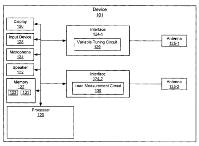
[0032] Fig. 1 depicts a schematic diagram of a device 101 for controlling an
antenna,
according to non-limiting implementations. Device 101 comprises a processor
120
interconnected with a memory 122, communications interfaces 124-1, 124-2, a
first
antenna 125-1, a second antenna 125-2, a display 126 and an input device 128,
and
optionally a microphone 134 and speaker 132. Communications interfaces 124-1,
124-2
will be interchangeably referred to, generically, as an interface 124, and
collectively as
interfaces 124. Antennas 125-1, 125-2 will be interchangeably referred to,
generically, as
an antenna 125, and collectively as antennas 125. Interface 124-1 further
comprises a
variable tuning circuit 129 for tuning antenna 125-1. Interface 124-2 further
comprises a
load measurement circuit 130 for measuring load on antenna 125-2. As will be
presently
explained, processor 120 is generally enabled to control antenna 125-1;
specifically,
processor 120 is enabled to: determine a load on second antenna 125-2; and,
control
variable tuning circuit 129 based on the load on second antenna 125-2 to
change a match
of first antenna 125-1. Hence, for example, when an object that affects the
load of
antennas 125 is proximal device 101, the load of second antenna 125-2 can be
determined, using load measurement circuit 130, and used to change a match of
first
antenna 125-1. Hence, for example, load changes due to loading objects,
including but
not limited to metallic objects, can be detected using second antenna 125-2
and used to
tune variable tuning circuit 129 to match first antenna 125-1.
[0033] Device 101 can be any type of electronic device that can be used in a
self:-
contained manner to communicate with one or more communication networks using
antennas 125. Device 101 includes, but is not limited to, any suitable
combination of
electronic devices, communications devices, computing devices, personal
computers,
laptop computers, portable electronic devices, mobile computing devices,
portable
computing devices, tablet computing devices, laptop computing devices, desktop
phones,
telephones, PDAs (personal digital assistants), cellphones, smartphones, e-
readers,
internet-enabled appliances and the like. Other suitable devices are within
the scope of
present implementations.
[0034] It should be emphasized that the structure of device 101 in Fig. 1 is
purely an
example, and contemplates a device that can be used for both wireless voice
(e.g.
CA 02818148 2015-03-24
telephony) and wireless data communications (e.g. email, web browsing, text,
and the
like). However, while Fig. 1 contemplates a device that can be used for
telephony, in
other implementations, device 101 can comprise a device enabled for
implementing any
suitable specialized functions, including but not limited to one or more of
telephony,
computing, appliance, and/or entertainment related functions.
[00351 Device 101 comprises at least one input device 128 generally enabled to
receive
input data, and can comprise any suitable combination of input devices,
including but not
limited to a keyboard, a keypad, a pointing device, a mouse, a track wheel, a
trackball, a
touchpad, a touch screen and the like. Other suitable input devices are within
the scope of
present implementations.
[00361 Input from input device 128 is received at processor 120 (which can be
implemented as a plurality of processors, including but not limited to one or
more central
processors (CPUs)). Processor 120 is configured to communicate with a memory
122
comprising a non-volatile storage unit (e.g. Erasable Electronic Programmable
Read Only
Memory ("EEPROM"), Flash Memory) and a volatile storage unit (e.g. random
access
memory ("RAM")). Programming instructions that implement the functional
teachings
of device 101 as described herein are typically maintained, persistently, in
memory 122
and used by processor 120 which makes appropriate utilization of volatile
storage during
the execution of such programming instructions. Those skilled in the art will
now
recognize that memory 122 is an example of computer readable media that can
store
programming instructions executable on processor 120. Furthermore, memory 122
is also
an example of a memory unit and/or memory module.
100371 In particular, it is appreciated that memory 122 stores an application
123 that,
when processed by processor 120, enables processor 120 to: determine a load on
second
antenna 125-2; and, control variable tuning circuit 129 based on the load on
second
antenna 125-2 to change a match of first antenna 125-1.
[00381 Memory 122 can further store data 131 for controlling variable tuning
circuit 129
based on the load on second antenna 125-2, data 131 associating the load on
second
antenna 125-2 to matching of first antenna 125-1 to radio equipment at
interface 124-1,
as will be described below. Data can be in any suitable format, including, but
not limited
to a look-up table, a database and the like. In general, data 131 comprises an
association
6
CA 02818148 2015-03-24
between data indicative of a load on second antenna 125-2 and one or more of
matching
impedance data for first antenna 125-1 and data for controlling variable
tuning circuit
129. In other words, there is an underlying assumption in data 131 that the
load on first
antenna 125-1 is related to the determined load on second antenna 125-2, such
that the
determined load on second antenna 125-2 can be used to control variable tuning
circuit
129.
[00391 Processor 120 can be further configured to communicate with display
126, and
optionally microphone 134 and speaker 132. Display 126 comprises any suitable
one of,
or combination of, CRT (cathode ray tube) and/or flat panel displays (e.g. LCD
(liquid
crystal display), plasma, OLED (organic light emitting diode), capacitive or
resistive
touchscreens, and the like). Microphone 134, when present, comprises any
suitable
microphone for receiving sound data. Speaker 132, when present, comprises any
suitable
speaker for providing sound data, audible alerts, audible communications from
remote
communication devices, and the like, at device 101.
100401 In some implementations, input device 128 and display 126 are external
to device
101, with processor 120 in communication with each of input device 128 and
display 126
via a suitable connection and/or link.
[00411 Processor 120 also connects to interfaces 124, each of which can be
implemented
as one or more radios and/or connectors and/or network adaptors, configured to
wirelessly communicate with one or more communication networks (not depicted)
via
antennas 125. It will be appreciated that each interface 124 is configured to
correspond
with network architecture that is used to implement one or more communication
links to
the one or more communication networks, including but not limited to any
suitable
combination of USB (universal serial bus) cables, serial cables, wireless
links, cell-phone
links, cellular network links (including but not limited to 20, 2.5G, 3G, 4G+,
UMTS
(Universal Mobile Telecommunications System), CDMA (Code division multiple
access), WCDMA (Wideband CDMA), FDD (frequency division duplexing), TDD (time
division duplexing), TDD-LTE (TDD-Long Term Evolution), TD-SCDMA (Time
Division Synchronous Code Division Multiple Access) and the like, wireless
data,
Bluetooth links, NFC (near field communication) links, WiFi links, WiMax
links, packet
7
CA 02818148 2015-03-24
based links, the Internet, analog networks, the PSTN (public switched
telephone
network), access points, and the like, and/or a combination.
[0042] Specifically, each of interfaces 124 comprises radio equipment (i.e. a
radio
transmitter and/or radio receiver) for receiving and transmitting signals
using respective
antennas 125.
[00431 It is further appreciated that variable tuning circuit 129 can comprise
any suitable
circuit for tuning antenna 125-1 at interface 124-1, for example by matching
impedance
of antenna 125-1 to the radio equipment. Variable tuning circuit 129 can hence
comprise
any suitable combination of capacitors and impedance coils (also referred to
as an
inductor) for matching impedance of antenna 125-1 to the radio equipment of
interface
124-1 when the loading on antenna 125-1 changes, for example when loading
objects
(e.g. metallic objects) are proximal device 101. Further, variable tuning
circuit 129 can be
controlled by processor 120.
100441 Similarly, load measurement circuit 130 can comprise any suitable
circuit for
measuring a load on antenna 125-2, and can hence comprise any suitable
combination of
signal transmitter, signal receiver, capacitors and impedance coils for
measuring a load
on antenna 125-2. It is further appreciated that load measurement circuit 130
is enabled to
generate and measure a signal. Specific non-limiting implementations of load
measurement circuit 130 are described below with reference to load measurement
circuits
130a, 130b of Figs. 4 and 5, respectively.
[004S) In specific non-limiting implementations, device 101 can comprise a
phone
device, first antenna 125-1 can comprise a main antenna, for example for
communicating
with a cell phone network, and second antenna 125-2 can comprise an NFC
antenna
and/or an NFC coil. Further, it is appreciated that NFC chipsets used in phone
devices
have the capability to measure the loading on the NFC antenna due to hands,
keys and
NFC devices. They have this capability to save power as they will transmit
only when the
NFC antenna is loaded past a certain threshold value as other nearby NFC
devices load
the NFC antenna: in other words, there is no point in transmitting signals
using the NFC
antenna unless the NFC antenna is loaded due to the nature of NFC devices. The
NFC
chipsets can hence detect loading by either measuring the resonance frequency
of the
NFC antenna and/or the capacitance of the NFC antenna, both of which change
due to
8
CA 02818148 2015-03-24
objects placed near the NFC antenna. Hence, in these implementations, the load
measurement circuit 130 comprises one or more NFC chipsets.
[0046] It is yet further appreciated that second antenna 125-2 can be at any
suitable
location in device 101, for example proximal first antenna 125-1, at a front
of device 101,
at a rear of device 101 and at a side of device 101. Further device 101 can
comprise a
plurality of antennas, similar to antenna 125-2, and a plurality of respective
load
measuring circuits, similar to load measuring circuit 130, to determine when
loading
objects are located proximal one or more of a front of the device and a rear
of the device.
[0047] It is yet further appreciated that device 101 comprises a power source,
not
depicted, for example a battery or the like. In some implementations the power
source
can comprise a connection to a mains power supply and a power adaptor (e.g.
and AC-to-
DC (alternating current to direct current) adaptor).
[0048] In any event, it should be understood that a wide variety of
configurations for
device 101 are contemplated.
[00491 Hence attention is now directed to Fig. 2 which depicts a flowchart of
a method
200 for controlling an antenna, according to non-limiting implementations. In
order to
assist in the explanation of method 200, it will be assumed that method 200 is
performed
using device 101 to control antennas 125 by controlling variable tuning
circuit 129.
Furthermore, the following discussion of method 200 will lead to a further
understanding
of device 101 and its various components. However, it is to be understood that
device
101 and/or method 200 can be varied, and need not work exactly as discussed
herein in
conjunction with each other, and that such variations are within the scope of
present
implementations.
[0050] It is appreciated that, in some implementations, method 200 is
implemented in
device 101 by a processor 120 processing application 123. It is further
appreciated that
aspects of method 200 can be implemented by one or more processors at
interfaces 124,
for example chipsets at interfaces 124. Indeed, method 200 is one way in which
device
101 can be configured. It is to be emphasized, however, that method 200 need
not be
performed in the exact sequence as shown, unless otherwise indicated; and
likewise
various blocks may be performed in parallel rather than in sequence; hence the
elements
of method 200 are referred to herein as "blocks" rather than "steps". It is
also to be
9
CA 02818148 2015-03-24
understood, however, that method 200 can be implemented on variations of
device 101 as
well.
100511 Further, the following discussion of method 200 will be done with
reference to
Figs. 3, which is similar to Fig. 1, with like elements having like numbers.
100521 At block 201, processor 120 determines a load on second antenna 125-2.
Specifically, data 301 is returned to processor 120 from load measurement
circuit 130,
data 301 indicative of load on antenna 125-2.
[00531 Load on antenna 125-2 can be determined in any suitable manner,
including, but
not limited to one or more of the following techniques:
100541 1. Measuring
a resonance frequency of second antenna 125-2. The
measurement of resonance frequency can be performed by one or more of
processor 120
controlling load measuring circuit 130 and by processor 120 communicating with
a
processor and/or chipset at load measuring circuit 130 that performs the
measurement and
communicates the measured resonance frequency and/or a measured load to
processor
120. For example, in these implementations, load measuring circuit 130 is
generally
enabled to sweep a frequency of a transmit signal provided to second antenna
125-2, for
exarnple by interface 124-2 and/or load measuring circuit 130, and measure one
or more
of a voltage and a current of a signal from second antenna 125-2; and,
determine the load
on second antenna 125-2 by determining a resonance frequency corresponding to
one or
more of a largest voltage and a largest current, the resonance frequency being
proportional to the load.
100551 An example of such a load measuring circuit 130a is depicted in Fig. 4,
which
depicts a portion of components of device 101: processor 120 is in
communication with
load measuring circuit 130a which in turn measures load on second antenna 125-
2. Load
measuring circuit 130a comprises a processor 420 which controls a frequency
sweep
circuit 430 for sweeping a frequency of a transmit signal provide to second
antenna 125-
2. Processor 420 can include, but is not limited to, an NFC chipset. The load
measurement hence results in a determination of a resonance frequency. The
measured
resonance frequency can be converted to load impedance or the measured
resonance
frequency can be used as an indication of load, with data 131 comprising an
association
between resonance frequencies and data for controlling variable tuning circuit
129. When
CA 02818148 2015-03-24
the measured resonance frequency is converted to load impedance, the
conversion can
occur at one or more of processor 120 and processor 420. In any event, it is
appreciated
that, in these implementations, load measurement circuit 130 comprises load
measurement circuit 130a of Fig. 4.
[0056] 2. Measuring
a capacitance of second antenna 125-2. For example, in these
implementations, load measuring circuit 130 generally comprises a variable
capacitor and
an impedance coil, and load measuring circuit 130 is generally enabled to
maintain a
given resonance frequency of the impedance coil by adjusting the variable
capacitor; the
load on second antenna 125-2 is determined by determining the change in
capacitance of
the variable capacitor, the change in capacitance generally appreciated to be
proportional
to loading on the impedance coil, and hence to loading on second antenna 125-
2.
[0057] An example of such a load measuring circuit 130b is depicted in Fig. 5,
which
depicts a portion of components of device 101: processor 120 is in
communication with
load measuring circuit 130b which in turn measures load on second antenna 125-
2. Load
measuring circuit 130b comprises a processor 520 which controls a variable
capacitor
530 to maintain a given resonance frequency on an impedance coil 540 connected
to
second antenna 125-2. Processor 520 can include, but is not limited to, an NFC
chipset.
The resonance frequency can be predetermined and can comprise, for example a
resonance frequency of antenna 125-2 when no loading objects are proximal
antenna
125-2. The load measurement hence results in a determination of a change in
capacitance
of variable capacitor 530. The change in capacitance can be converted to load
impedance
or the change in capacitance can be used as an indication of load, with data
131
comprising an association between capacitance (and/or capacitance changes) and
data for
controlling variable tuning circuit 129. When the change in capacitance is
converted to
load impedance, the conversion can occur at one or more of processor 120 and
processor
520. In any event, it is appreciated that, in these implementations, load
measurement
circuit 130 comprises load measurement circuit 130b of Fig. 5.
[0058] Returning to Figs. 2 and 3, at block 201, processor 120 receives data
301 from
load measurement circuit 130 to determine the load on second antenna 125-2.
Processor
120 optionally converts resonance frequency data, capacitance data therein to
load
impedance data.
CA 02818148 2015-03-24
[0059] In any event, at block 203, processor compares data 301 (and optionally
converted
data) to data 131 to determine a match for first antenna 125-1, and
specifically data for
controlling variable tuning circuit 129 to match first antenna 125-1 to radio
equipment at
interface 124-1. The data for controlling variable tuning circuit 129 can be
retrieved from
data 131 using data 301 and/or can be derived by using data 301 to retrieve a
matching
impedance for first antenna 125-1 from data 131 and processing the matching
impedance
to determine the data to control variable tuning circuit 129.
[0060] In any event, at block 205, processor 120 controls variable tuning
circuit 129
based on the load determined at block 201 to change a match of first antenna
125-1. For
example, in depicted implementations, processor 120 transmits control data 303
to
interface 124-1, which is used to control variable tuning circuit 129 to match
first antenna
125-1 with radio equipment at interface 124-1.
[0061] It is further appreciated that method 200 can be implemented at any
suitable time
and with any suitable periodicity. For example, it is appreciated that in
implementations
where second antenna 125-2 comprises an NFC antenna, the associated NFC
chipset (e.g.
processor 420, 520) is monitoring second NFC antenna 125-2 for changes in load
as part
of a normal function of an NFC chipset. In these implementations, processor
120 can be
implementing method 200 in the background such that block 201 is implemented
repeatedly, and blocks 203, 205 occur when load changes are determined at
block 201.
[0062] In other implementations, method 200 and/or block 201 is implemented
periodically, for example every few seconds or the like.
[0063] In yet further implementations, device 101 further comprises one or
more
proximity sensors and method 200 is implemented only when proximity of an
object is
detected using the one or more proximity sensors. For example, attention is
directed to
Fig. 6, which depicts a device 101a similar to device 101 but comprising a
proximity
sensor 601. While Fig. 6 is a perspective view of device 101a, it is
appreciated that
device 101a has a schematic structure similar to that of device 101 as
depicted in Fig. 1,
with a processor of device 101a implementing method 200 only when proximity
sensor
601 determines that an object 603 is proximal device 101a. The proximity
sensor 601
can comprise any suitable proximity sensor, including, but not limited to, IR
(infrared)
diode/detectors, capacitive sensors, capacitive displacement sensors, Doppler
effect
12
CA 02818148 2013-06-06
sensors, eddy-current sensor, inductive sensors, laser sensors, optical
sensors, acoustic
sensors, magnetic sensors, passive optical sensors (such as charge-coupled
devices),
passive thermal infrared sensors, photocell sensors (reflective), and the
like.
100641 A non-limiting example scenario of use of method 200 is now described.
In this
scenario, a main antenna can be located on a front-top of a device that is
highly affected
by objects placed near an audio receiver. Near the audio receiver an IR
diode/detector can
determine whether an object is in front of the device, and near the main
antenna but it
cannot determine whether it is a metallic object or a non metallic object such
as wood or
skin. Metallic and non-metallic objects have different effects on antenna
tuning and the
device may make the wrong guess in changing a variable antenna match that
could result
in lower performance. In any event, when the IR sensor detects an object, the
device
implements method 200 and one or more NFC coils/antennas located in the front
of the
device in locations such as behind a display, around the display or around the
receiver
can be probed to determine a resonance frequency. Metallic objects have a
great affect on
the resonance frequency of an NFC antenna while organic objects do not.
Combining the
proximity sensor data with the NFC coil data the phone can determine whether
there is no
object (i.e. no object sensed by the IR sensor), an organic object (i.e. an
object is sensed
by the IR sensor but no change in load is determined at the NFC antenna) or
metallic
object located in front of the device (i.e. an object is sensed by the IR
sensor and a change
in load is determined at the NFC antenna). In some implementations, a size of
the
metallic object and/or distance between the device and the metallic object can
be
estimated depending on how large a determined frequency shift, for example, is
for the
NFC antenna. Using this information the device can then tune the main antenna
to
compensate for the object in front of the device. It is, however, appreciated,
that NFC
antennas can be placed in other strategic locations to help detect loading for
antennas in
different sections of the phone.
[0065] Hence, convenient devices and methods for controlling an antenna are
described
herein that better enable matching of antennas to radio equipment. Further,
these methods
can be cheaply and conveniently implemented using a combination of a main
processor
of a device and existing NFC chipsets.
13
CA 02818148 2013-06-06
[0066] Those skilled in the art will appreciate that in some implementations,
the
functionality of devices 101, 101a can be implemented using pre-programmed
hardware
or firmware elements (e.g., application specific integrated circuits (ASICs),
electrically
erasable programmable read-only memories (EEPROMs), etc.), or other related
components. In other implementations, the functionality of devices 101, 101a
can be
achieved using a computing apparatus that has access to a code memory (not
shown)
which stores computer-readable program code for operation of the computing
apparatus.
The computer-readable program code could be stored on a computer readable
storage
medium which is fixed, tangible and readable directly by these components,
(e.g.,
removable diskette, CD-ROM, ROM, fixed disk, USB drive). Furthermore, it is
appreciated that the computer-readable program can be stored as a computer
program
product comprising a computer usable medium. Further, a persistent storage
device can
comprise the computer readable program code. It is yet further appreciated
that the
computer-readable program code and/or computer usable medium can comprise a
non-
transitory computer-readable program code and/or non-transitory computer
usable
medium. Alternatively, the computer-readable program code could be stored
remotely but
transmittable to these components via a modem or other interface device
connected to a
network (including, without limitation, the Internet) over a transmission
medium. The
transmission medium can be either a non-mobile medium (e.g., optical and/or
digital
and/or analog communications lines) or a mobile medium (e.g., microwave,
infrared,
free-space optical or other transmission schemes) or a combination thereof.
[0067] A portion of the disclosure of this patent document contains material
which is
subject to copyright protection. The copyright owner has no objection to the
facsimile
reproduction by any one of the patent document or patent disclosure, as it
appears in the
Patent and Trademark Office patent file or records, but otherwise reserves all
copyrights
whatsoever.
[0068] Persons skilled in the art will appreciate that there are yet more
alternative
implementations and modifications possible, and that the above examples are
only
illustrations of one or more implementations. The scope, therefore, is only to
be limited
by the claims appended hereto.
14