Note: Descriptions are shown in the official language in which they were submitted.
CA 02818205 2013-06-06
253411-3
THREE-LEVEL PHASE LEG FOR A POWER CONVERTER
BACKGROUND OF THE INVENTION
[0001] The subject matter described herein relates generally to power
conversion within electric power systems, and more specifically, to low-
inductance,
three-level, neutral point clamped (NPC) power converters for electric power
generation
assets.
[0002] Generally, a wind turbine includes a rotor that includes a
rotatable hub assembly having multiple blades. The blades transform wind
energy into a
mechanical rotational torque that drives one or more generators via the rotor.
At least
some of the known wind turbines are physically nested together in a common
geographical region to form a wind turbine farm. Variable speed operation of
the wind
turbine facilitates enhanced capture of energy when compared to a constant
speed
operation of the wind turbine. However, variable speed operation of the wind
turbine
produces electric power having varying voltage and/or frequency. More
specifically, the
frequency of the electric power generated by the variable speed wind turbine
is
proportional to the speed of rotation of the rotor. A power converter may be
coupled
between the wind turbine's electric generator and an electric utility grid.
The power
converter receives electric power from the wind turbine generator and
transmits
electricity having a fixed voltage and frequency for further transmission to
the utility grid
via a transformer. The transformer may be coupled to a plurality of power
converters
associated with the wind turbine farm.
[0003] Many known power converters include a plurality of power
conversion devices, i.e., power modules that include semiconductor devices
such as
insulated gate bipolar transistors (IGBTs). The IGBTs, other electronic
devices, and the
associated electrically conductive connections that form the power modules
have known
inductances and the associated impedances. The impedances are proportional to
the
frequencies of the signals transmitted therethrough. As such, transmitting
electric current
1
CA 02818205 2013-06-06
253411-3
through such power modules at high switching frequencies induces
electromagnetic fields
that may induce unwanted voltages and currents, thereby increasing switching
losses and
voltage overshoots. Significantly, some diode devices will experience a
reverse recovery
that induces a voltage and current spike that is transmitted through briefly-
formed
commutation loops. The deleterious effects of such commutation loops are
proportional
to the associated inductance of the loops, and such effects may include high
voltage
stresses on the semiconductor devices. Moreover, such unwanted voltages and
currents
may include harmonics affecting the power quality of the electric power
transmitted from
the power converters. As the switching losses increase and demands for more
robust
power converters escalate, the size, weight, and cost of the power modules,
and,
therefore, the power converters, increase proportionally to compensate.
[0004] Three-level bridge configurations that generate three voltages,
i.e., a positive voltage, a neutral voltage, and a negative voltage,
facilitate faster power
converter switching speeds, i.e., rates of voltage transitions measured at the
output
terminals of the converter, than other bridge configurations, thereby
facilitating improved
power quality. However, configuring such three-level bridges, with the
associated heat
sinks, as well as the power conversion components and the conductors
therebetween,
significantly increases the challenges associated with maintaining the
inductances of the
power modules low enough to reduce the negative impact of higher switching
speeds of
the power converters. Limiting the switching speeds of the power converters
due to the
inherent inductances of the modules therein limits the performance advantages
associated
with the higher switching speeds, and facilitates increased size, weight, and
cost of power
converters.
BRIEF DESCRIPTION OF THE INVENTION
[0005] In one aspect, a phase leg for a three-level power converter is
provided. The phase leg includes a heat sink device that includes a first
surface and a
second surface opposite the first surface. The phase leg also includes a first
portion
including at least one semiconductor switching device coupled to the first
surface. The
2
I
CA 02818205 2013-06-06
253411-3
phase leg further includes a second portion including at least one
semiconductor
switching device coupled to the second surface.
[0006] In another aspect, a phase leg for a three-level power converter is
provided. The phase leg includes a plurality of non-neutral planar bus bars, a
plurality of
semiconductor switching devices coupled to at least one of the non-neutral
planar bus
bars, and a neutral planar bus bar. The non-neutral planar bus bars, the
semiconductor
switching devices, and the neutral planar bus bar are configured to define at
least one
commutation loop within the phase leg. The non-neutral planar bus bars and the
neutral
planar bus bar are configured and oriented to facilitate flux cancellation in
the
commutation loop when current flows therethrough, thereby facilitating a
reduction of
energy stored within loop currents induced therein.
[0007] In yet another aspect, a two-layer, direct current (DC) link
assembly for a three-level power converter is provided. The DC link assembly
includes a
first layer including a positive planar bus bar and an adjacent negative
planar bus bar
separated with a spacing therebetween. The DC link assembly also includes a
second
layer including a neutral planar bus bar sized to substantially similar
dimensions as the
first layer. The DC link assembly further includes an insulator positioned
between the
first layer and the second layer. The insulator is sized to completely extend
over the
second layer. The DC link assembly also includes at least one phase leg module
coupled
to the first layer and the second layer.
BRIEF DESCRIPTION OF THE DRAWINGS
[0008] FIG. 1 is a schematic view of an exemplary wind turbine.
[0009] FIG. 2 is a schematic view of an exemplary power conversion
and transmission system that may be used with the wind turbine shown in FIG.
I.
[0010] FIG. 3 is a schematic overhead view of an exemplary power
converter that may be used with the system shown in FIG. 2.
3
I
CA 02818205 2013-06-06
253411-3
[0011] FIG. 4 is a schematic view of an exemplary three-level phase leg
circuit that may be used with the power converter shown in FIG. 3.
[0012] FIG. 5 is a schematic side view of the three-level phase leg
circuit shown in FIG. 4 with a neutral connection coupled thereto.
[0013] FIG. 6 is a schematic side view of the three-level phase leg
circuit shown in FIG. 4 with a positive connection and a negative connection
coupled
thereto.
[0014] FIG. 7 is a schematic perspective view of a portion of the three-
level phase leg circuit shown in FIG. 4.
[0015] FIG. 8 is a schematic perspective view of the portion of the three-
level phase leg circuit shown in FIG. 7.
[0016] FIG. 9 is a frontal view of an exemplary two-layer, direct current
(DC) link assembly that can be used with the three-level power converter shown
in FIG.
3.
[0017] FIG. 10 is a schematic view of a plurality of exemplary small
commutating loops in the three-level phase leg circuit shown in FIG. 4.
[0018] FIG. 11 is a schematic view of a plurality of exemplary large
commutating loops in the three-level phase leg circuit shown in FIG. 4.
DETAILED DESCRIPTION OF THE INVENTION
[0019] As used herein, the term "blade" is intended to be representative
of any device that provides reactive force when in motion relative to a
surrounding fluid.
As used herein, the term "wind turbine" is intended to be representative of
any device that
generates rotational energy from wind energy, and more specifically, converts
kinetic
energy of wind into mechanical energy. As used herein, the term "electric
power
generation device" is intended to be representative of any device that
provides electric
4
CA 02818205 2013-06-06
253411-3
power derived from an energy resource. As used herein, the term "wind turbine
generator" is intended to be representative of any wind turbine that includes
an electric
power generation device that generates electrical power from rotational energy
generated
from wind energy, and more specifically, converts mechanical energy converted
from
kinetic energy of wind to electrical power.
[0020] Technical effects of the apparatus and systems described herein
include at least one of: (a) facilitating the use of three-level bridge
configurations in
power converters while using a two-layer bus structure; (b) decreasing the
inductance of
commutating loops defined in a three-level bridge configuration, thereby
facilitating flux
cancellation in the commutation loops when current flows therethrough, thereby
facilitating a reduction of energy stored within loop currents induced therein
through
routine switching actions; (c) increasing the switching speed of power
converters for a
given IGBT switching frequency as compared to other bridge configurations; (d)
increasing the output voltage of power converters as compared to other bridge
configurations; (e) improving the power quality by reducing the harmonics for
similar
switching speeds of power converters as compared to other bridge
configurations; (1)
increasing heat removal capabilities by "folding" a three-level bridge
assembly to use at
least two sides of a heat sink for more effective heat removal as compared to
bridge
circuits without heat sinks or using only one side of a heat sink, thereby
facilitating an
increase in a power rating of the bridge circuit; (g) increasing power ratings
of power
converters without equivalent increases in size and weight; (h) separating the
positive and
negative terminals of a three-level bridge configuration such that heat-
generating power
conversion devices may be positioned on opposite sides of a heat sink device;
and (i)
facilitating low inductance interconnections of portions of a three-level
phase leg
positioned on opposite sides of a heat sink.
[0021] The apparatus and systems described herein facilitate
transmitting electric power from renewable and non-renewable electric power
generation
assets. Also, the apparatus and systems described herein facilitate
transmitting electric
power to electric motor drive devices. Specifically, the apparatus and systems
described
I i
CA 02818205 2013-06-06
253411-3
herein facilitate generating and transmitting increased electric power using
power
converters with a smaller physical footprint. More specifically, the apparatus
and
systems described herein facilitate using single IGBTs and diodes in a low-
inductance,
three-level bridge, neutral point clamped (NPC) configuration in power
converters,
thereby facilitating an increase in the switching speeds and the power ratings
of the
power converters without similarly increasing the size of the power
converters.
[0022] Although generally described herein with respect to a wind
turbine facility, the systems described herein are applicable to any type of
electric
systems including, for example, and without limitation, renewable energy
sources such as
solar power generation systems, fuel cells, geothermal generators, hydropower
generators, non-renewable energy sources such as fossil and nuclear power
plants, and
motor drive devices.
[0023] FIG. 1 is a schematic view of an exemplary wind turbine
generator 100. Wind turbine generator 100 is an electric power generation
device
including a nacelle 102 housing a generator (not shown in FIG. 1). Nacelle 102
is
mounted on a tower 104 (a portion of tower 104 being shown in FIG. 1). Tower
104 may
be any height that facilitates operation of wind turbine generator 100 as
described herein.
Wind turbine generator 100 also includes a rotor 106 that includes three rotor
blades 108
attached to a rotating hub 110. Alternatively, wind turbine generator 100
includes any
number of blades 108 that facilitates operation of wind turbine generator 100
as described
herein. In the exemplary embodiment, wind turbine generator 100 includes a
gearbox
(not shown in FIG. 1) rotatably coupled to rotor 106 and a generator (not
shown in FIG.
1). While only one wind turbine generator 100 is shown, a plurality of wind
turbine
generators 100 may be at least partially grouped geographically and/or
electrically to
define a renewable energy generation facility, i.e., a wind turbine farm (not
shown in
FIG. 1). Such a wind turbine farm may be defined by a number of wind turbine
generators 100 in a particular geographic area, or alternatively, defined by
the electrical
connectivity of each wind turbine generator 100 to a common substation.
6
i
CA 02818205 2013-06-06
253411-3
[0024] FIG. 2 is a schematic view of an exemplary power conversion
and transmission system 111 that may be used with wind turbine generator 100.
Wind
turbine generator 100 is a renewable energy source that includes an electric
power
generator 112 coupled to a first power source, i.e., a power converter 114,
through a
plurality of input conduits 115 (only one shown in FIG. 2). Electric power
generator 112
is any type of generator that enables operation of wind turbine generator 100
as described
herein, including, without limitation, a synchronous permanent magnet
generator (PMG),
an electrically excited synchronous generator (EESG), and a doubly-fed
induction
generator (DFIG).
[0025] Power converter 114 is any device that enables operation of wind
turbine generator 100 as described herein, including, without limitation, a
full power
conversion assembly. In the exemplary embodiment, electrical, three-phase,
sinusoidal,
AC power is generated within electric power generator 112 and is transmitted
to power
converter 114 through input conduits 115. Within power converter 114, the
electrical
power is rectified in a converter portion (not shown in FIG. 2) from
sinusoidal, three-
phase AC power to direct current (DC) power. The DC power is transmitted to an
inverter (not shown in FIG. 2) that converts the DC electrical power to three-
phase,
sinusoidal AC electrical power with regulated voltages, currents, and
frequencies. Power
converter 114 compensates or adjusts the frequency of the three-phase power
from
electric power generator 112 for changes, for example, in the wind speed at
hub 110 and
blades 108 (both shown in FIG. 1). Therefore, in this manner, mechanical and
electrical
rotor frequencies are decoupled from grid frequency.
[0026] Power converter 114 is coupled to an electric power grid 116 via
a plurality of output conduits 117 (only one shown in FIG. 2), a main
transformer 118, a
main transformer circuit breaker 120, and a main transformer bus 122. When
circuit
breaker 120 is closed, three-phase AC electric power is transmitted from power
converter
114 to electric power grid 116 for further transmission and distribution.
7
I
CA 02818205 2013-06-06
253411-3
[0027] While only one wind turbine generator 100 is shown, a plurality
of wind turbine generators 100 may be at least partially grouped
geographically and/or
electrically to define a renewable energy generation facility, i.e., a wind
turbine farm 124.
Each wind turbine generator 100 is coupled to main transformer bus 122 through
a
substation bus 126. Such wind turbine farm 124 may be defined by a number of
wind
turbine generators 100 in a particular geographic area, or alternatively,
defined by the
electrical connectivity of each wind turbine generator 100 to a common
substation.
[0028] In some alternative embodiments, a combination of electric
power generation devices are used in conjunction with, or in place of, wind
turbine
generator 100. In at least one alternative embodiment, wind turbine generator
100 is
replaced with solar panels (not shown) coupled to form one or more solar
arrays (not
shown) to facilitate operating at a desired power output with supplemental,
solar-
generated power. Solar panels include, in one alternative embodiment, one or
more of a
photovoltaic panel, a solar thermal collector, or any other device that
converts solar
energy to electrical energy. In such alternative embodiments, each solar panel
is a
photovoltaic panel that generates a substantially direct current power as a
result of solar
energy striking solar panels.
[0029] Also, in such alternative embodiments, each solar array is
coupled to a power converter that is similar to at least a portion of power
converter 114
that converts the DC power to AC power that is transmitted to a transformer
similar to
transformer 118 and then to grid 116. Furthermore, although generally
described herein
with respect to wind turbine generator 100 and a solar array facility, the
systems
described herein are applicable to any type of electric generation system
including, for
example, fuel cells, geothermal generators, hydropower generators, and/or
other devices
that generate power from renewable and/or non-renewable energy sources.
[0030] FIG. 3 is a schematic overhead view of power converter 114 that
may be used with power conversion and transmission system 111 (shown in FIG.
2).
Each of three input conduits 115 is configured such that the input current is
split between
8
i
CA 02818205 2013-06-06
253411-3
each conduit 115. At least one boost inductor 130 is coupled to each of input
conduits
115. Boost inductors 130 facilitate filtering the input voltage and/or current
received
from generator 112 (shown in FIG. 2). In addition, at least a portion of the
energy
received from generator 112 is temporarily stored within each boost inductor
130.
[0031] In the exemplary embodiment, power converter 114 includes an
AC-to-DC converter portion 132 and a DC-to-AC inverter portion 134 coupled
together
by a DC bus system 136. Therefore, power converter 114 is a full power
converter.
Alternatively, for those embodiments that include electric power generation
devices such
as, without limitation, solar arrays, that generate a DC voltage, converter
portion 132 may
be replaced with, or supplemented with, a DC-to-DC boost converter. Moreover,
in the
exemplary embodiment, DC bus system 136 includes capacitors 138, i.e.,
capacitors 138P
and 138N. Alternatively, DC bus system 136 includes any number of capacitors
138
and/or any other electrical power storage devices that enable power converter
114 to
function as described herein. DC bus system 136 also includes a positive rail
140 and a
negative rail 142. At least one filtering inductor 144 is coupled to each of
output conduits
117. Inductors 144 facilitate filtering the output voltage and/or current
transmitted from
inverter portion 134.
[0032] In operation, converter portion 132 is coupled to, and receives
AC power from, generator 112 through input conduits 115. Converter portion 132
rectifies the AC power to a predetermined DC voltage. As power is transmitted
through
converter portion 132, a DC voltage is induced across DC bus system 136 and
energy is
stored within capacitors 138. Inverter portion 134 converts DC power
transmitted from
DC bus system 136 into AC power for transmission to electric power grid 116
(shown in
FIG. 2) through output conduits 117.
[0033] In the exemplary embodiment, both converter portion 132 and
inverter portion 134 include a plurality of phase legs 150, i.e., one phase
leg 150 for each
of the three phases transmitted from generator 112 and transmitted to grid
116. Each of
legs 150 includes an upper portion 152 and a lower portion 154 coupled
together in serial
9
CA 02818205 2013-06-06
253411-3
arrangement for each phase of electrical power that power converter 114
generates. For
each phase leg 150 in converter portion 132, upper portion 152 extends between
positive
rail 140 and input conduit 115 and lower portion 154 extends between negative
rail 142
and input conduit 115. Also, for each phase leg 150 in inverter portion 134,
upper
portion 152 extends between positive rail 140 and output conduit 117 and lower
portion
154 extends between negative rail 142 and output conduit 117. Each of legs 150
include
a neutral bus connection 156 coupled to each of upper portion 152 and lower
portion 154,
thereby defining power converter 114 as a three-level converter that
facilitates a bridge
configuration that generates three voltages, i.e., a positive voltage, a
neutral voltage, and
a negative voltage.
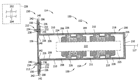
[0034] FIG. 4 is a schematic view of an exemplary three-level phase leg
circuit 200 of one phase leg 150 of inverter portion 134 (shown in FIG. 3) of
power
converter 114 (shown in FIG. 3). All six phase legs 150 are substantially
identical with
the principle exception that three of the six phase legs 150 are coupled to
input conduits
115 (shown in FIG. 3) and the other three phase legs 150 are coupled to output
conduits
117. Otherwise, each phase leg 150 of converter portion 132 (shown in FIG. 3)
and
inverter portion 134 are substantially similar and each includes upper and
lower portions
152 and 154, respectively, coupled in series. Three-level phase leg circuit
200 is coupled
to an upper capacitor 202 and a lower capacitor 204, wherein capacitors 202
and 204 are
a portion of a larger DC link assembly (not shown in FIG. 4 and described
further below)
external to portions 152 and 154. Three-level phase leg circuit 200 also
includes a
positive bus 206 coupled to upper capacitor 202, a negative bus 208 coupled to
lower
capacitor 204, and a midpoint, or neutral bus 210 also coupled to capacitors
202 and 204.
Neutral bus 210 is coupled to neutral bus connection 156 through at least one
neutral
terminal 212 (two shown in FIG. 4). Also, neutral bus 210 extends proximate to
portions
152 and 154 and extends over positive bus 206 and negative bus 208 with a
dielectric
material (not shown in FIG. 4) therebetween.
[0035] In the exemplary embodiment, upper portion 152 includes two
semiconductor switching devices, i.e., outer switching device Si and inner
switching
CA 02818205 2013-06-06
253411-3
device S2. Switching devices Si and S2 are coupled in series through a first
switch
interconnect bus 209 that includes an extension 209E. In the exemplary
embodiment,
switching devices Si and S2 are insulated gate bipolar transistors (IGBTs).
Alternatively, switching devices Si and S2 are any other suitable transistor
or any other
suitable switching device, including, without limitation, gate turn-off
thyristors (GT0s).
Antiparallel, i.e., inverse diodes D1 and D2 are coupled in parallel with
switching devices
Si and S2, respectively.
[0036] Also, in the exemplary embodiment, upper portion 152 includes a
clamping diode D5 coupled to neutral bus 210 through at least one, e.g.,
three, anode
terminals A and a neutral bus extension 210E1. Alternatively, clamping diode
D5 is
coupled to neutral bus 210 through any number of anode terminals A that
enables
operation of three-level phase leg circuit 200 as described herein. Clamping
diode D5 is
also coupled to the output of switching device Si and the input of switching
device S2
through a at least one, e.g., three, cathode terminals K coupled to first
switch interconnect
bus 209 through first switch interconnect bus 209E. Alternatively, clamping
diode D5 is
coupled to first switch interconnect bus 209 through any number of cathode
terminals K
that enables operation of three-level phase leg circuit 200 as described
herein. The input
of switching device Si is coupled to positive bus 206 and the output of device
Si is
coupled to clamping diode D5 and the input to switching device S2 through
first switch
interconnect bus 209. The output of switching device S2 is coupled to output
conduit 117
and an output conduit connection portion 218 (described further below).
[0037] Further, in the exemplary embodiment, lower portion 154
includes an inner switching device S3 and outer switching device S4. Switching
devices
S3 and S4 are coupled in series through a second switch interconnect bus 211,
that
includes an extension 211E, and are substantially similar to devices S 1 and
S2.
Antiparallel, i.e., inverse diodes D3 and D4 are coupled in parallel with
switching devices
S3 and S4, respectively.
11
CA 02818205 2013-06-06
253411-3
[0038] Moreover, in the exemplary embodiment, lower portion 154
includes a clamping diode D6 coupled to neutral bus 210 through at least one,
e.g., three,
cathode terminals K and a neutral bus extension 210E2. Alternatively, clamping
diode
D6 is coupled to neutral bus 210 through any number of cathode terminals K
that enables
operation of three-level phase leg circuit 200 as described herein. Clamping
diode D6 is
also coupled to the output of switching device S3 and the input of switching
device S4
through at least one, e.g., three, anode terminals A coupled to second switch
interconnect
bus 211 through second switch interconnect bus 211E. Alternatively, clamping
diode D6
is coupled to second switch interconnect bus 211 through any number of anode
terminals
A that enables operation of three-level phase leg circuit 200 as described
herein.
Clamping diode D6 is similar to clamping diode D5, with the exception that
diode D6 is
reversed with respect to diode D5. The input of switching device S3 is coupled
to output
conduit 117 and output conduit connection portion 218 (described further
below), and the
output of device S3 is coupled to clamping diode D6 and the input to switching
device
S4. The output of switching device S4 is coupled to negative bus 208.
[0039] Also, in the exemplary embodiment, each of switching devices
Si, S2, S3, and S4 includes a plurality of control connections. Specifically,
each
switching device Sl, S2, S3, and S4 includes gate and emitter control
connections GE I,
GE2, GE3, and GE4, respectively. Gate and emitter control connections GE1,
GE2,
GE3, and GE4 are each coupled to an individual drive circuit (not shown) that
controls
the switching action of associated switching devices Si, S2, S3, and S4,
respectively.
Alternatively, any control configuration that enables operation of three-level
phase leg
circuit 200 and power converter 114 as described herein is used.
[0040] Moreover, in the exemplary embodiment, each of switching
devices Si, S2, S3, and S4 includes a plurality, e.g., three, of collector (C)
terminals and
a plurality of emitter (E) terminals. Alternatively, any number of C terminals
and E
terminals are used that enable operation of three-level phase leg circuit 200
as described
herein. Therefore, for an illustrative example, clamping diode D5 is coupled
to S2E,
12
i
CA 02818205 2013-06-06
253411-3
S3C, and neutral bus 210. Similarly, clamping diode D6 is coupled to S3E, S4C
and
neutral bus 210.
[0041] In addition to those components described and shown on three-
level phase leg circuit 200, additional components may be added to increase
the
flexibility of operation and application of circuit 200. For example, without
limitation,
additional components may include IGBTs, resistors, and thermistors in
parallel to
switches Si through S4.
[0042] Moreover, in the exemplary embodiment, switching devices S2
and S3 are coupled to each other and output conduit 117 through an output
conduit
connection portion 218. Positive bus 206, negative bus 208, neutral bus 210,
first switch
interconnect bus 209, second switch interconnect bus 211, and output conduit
connection
portion 218 are formed and oriented as low inductance planar bus bars that
facilitate a
low interconnect inductance within three-level phase leg circuit 200. Also,
the portion of
neutral bus 210 extending between terminals D5A and D6K that is positioned
proximate
to a current path defined by terminals D5K, S2C, S2E, S3C, S3E, and D6A at
least
partially defines a commutation path (discussed further below).
[0043] FIG. 5 is a schematic side view of three-level phase leg circuit
200 with neutral bus connection 156 coupled thereto. FIG. 5 is based on the
portion of
FIG. 9 taken along line 5-5 (shown in FIG. 9). Three-level phase leg circuit
200 and
neutral bus connection 156 are portions of a two layer, DC link assembly (not
shown in
FIG. 5 and described further below.) In the exemplary embodiment, each phase
leg 150
includes a heat sink device 222 that includes a first surface 224 and an
opposing second
surface 225. Components of first portion 152 of phase leg 150 are coupled to
first surface
224. Specifically, semiconductor switching devices Si and S2, inverse diodes
D1 and
D2, and clamping diode D5 (shown in FIG. 4) are coupled to first surface 224.
Similarly,
components of second portion 154 of phase leg 150 are coupled to second
surface 225.
Specifically, semiconductor switching devices S3 and S4, inverse diodes D3 and
D4, and
clamping diode D6 (shown in FIG. 4) are coupled to second surface 225.
13
I I
CA 02818205 2013-06-06
253411-3
[0044] Therefore, in the exemplary embodiment, three-level phase leg
circuit 200 is "folded over", i.e., wrapped around heat sink device 222. Each
phase leg
150 is configured with components of first portion 152 and second portion 154
coupled to
heat sink device 222 and positioned on opposing surfaces 224 and 225,
respectively, of
heat sink device 222. Heat transfer is removed from heat sink device 222
through any
heat transfer means that enables operation of three-level phase leg circuit
200 and power
converter 114 as described herein, including, without limitation, fluid-
cooling, e.g.,
refrigerant-cooling, water-cooling, and air-cooling.
[0045] Also, in the exemplary embodiment, a non-conducting,
electrically-insulating material 226 is positioned between neutral bus 210 and
each of
busses 206, 208, 209, 211, and 218 to decrease the potential for a short
circuit between
them.
[0046] Further, in the exemplary embodiment, positive bus 206, negative
bus 208, first switch interconnect bus 209, second switch interconnect bus
211, output
conduit connection portion 218, and portions of neutral bus 210 are formed and
oriented
to define a low inductance planar bus bar configuration that facilitates a low
interconnect
inductance within three-level phase leg circuit 200. Neutral bus 210 is formed
and
oriented to be substantially parallel to busses 206, 208, 209, 211, and 218 to
facilitate
such low interconnect inductance. Also, neutral bus 210 is positioned with a
spacing
between bus 210 and busses 206, 208, 209, 211, and 218 sized to further
facilitate a low
interconnect inductance within three-level phase leg circuit 200. Further,
each of busses
206, 208, 209, 210, 211, and 218 are sized with a predetermined width and
insulator 226
is sized with a predetermined thickness such that a thickness value of
insulator 226 is
small as compared to a width value of busses 206, 208, 209, 210, 211, and 218.
For
example, and without limitation, a bus width-to-insulator thickness ratio is
approximately
10:1.
[0047] Moreover, in the exemplary embodiment, upper capacitor 202
and lower capacitor 204 are positioned within a capacitor bank 228. Any number
of
14
I
CA 02818205 2013-06-06
253411-3
capacitors may be positioned in capacitor bank 228, including, without
limitation, the
capacitors (not shown) for the remaining phase legs 150 (shown in FIG. 3).
Also, upper
capacitor 202 is coupled directly to positive rail 140 and neutral bus
connection 156
(coupling not shown in FIG. 5 for clarity) using any method that enables
operation of
three-level phase leg circuit 200 and power converter 114 as described herein.
Similarly,
lower capacitor 204 is coupled directly to negative rail 142 and neutral bus
connection
156 (coupling not shown in FIG. 5 for clarity) using any method that enables
operation of
three-level phase leg circuit 200 and power converter 114 as described herein.
Upper
capacitor 202 and lower capacitor 204 are configured to serve all six phase
legs 150
within a larger DC link assembly (not shown in FG. 5 and discussed further
below).
[0048] Also, in the exemplary embodiment, three-level phase leg circuit
200 is coupled to neutral bus connection 156 through a neutral bus coupling
apparatus
230. Neutral bus coupling apparatus 230 includes neutral bus terminals 212
that include
a fastener 232, a receptacle 234, and a conductive bushing 236 deposited
within a void
238 defined within positive rail 140 and positive bus 206 and a void 240
defined within
negative rail 142 and negative bus 208. Fastener 232 extends through and
contacts
neutral bus 210 and neutral bus connection 156 to induce a contact force
between neutral
bus 210 and conductive bushing 236 and inducing a contact force between
conductive
bushing 236 and neutral bus connection 156 such that neutral bus 210 is
maintained at
substantially the same potential as connection 156. Neutral bus coupling
apparatus 230
also includes an insulator 242 between positive rail 140 and neutral bus
connection 156
and negative rail 142 and neutral bus connection 156.
[0049] Further, in the exemplary embodiment, neutral bus coupling
apparatus 230 facilitates coupling neutral bus connection 156 to neutral bus
210 and
forming and orienting neutral bus 210 as low inductance planar bus bars
substantially
parallel to busses 206, 208, 209, and 211 to facilitate a low interconnect
inductance.
[0050] FIG. 6 is a schematic side view of three-level phase leg circuit
200 with a positive bus coupling apparatus 250 and a negative bus coupling
apparatus
P
I
CA 02818205 2013-06-06
253411-3
260 coupled thereto. FIG. 6 is based on the portion of FIG. 9 taken along line
6-6 (shown
in FIG. 9). Three-level phase leg circuit 200, positive bus coupling apparatus
250, and a
negative bus coupling apparatus 260 are portions of a two layer, DC link
assembly (not
shown in FIG. 6 and described further below.) In the exemplary embodiment,
three-level
phase leg circuit 200 is coupled to positive bus coupling apparatus 250
through a positive
bus terminal 252. Positive bus terminal 252 includes a fastener 254 inserted
into a
receptacle 256. A void 258 is formed within neutral bus connection 156 to
accept
receptacle 256. Fastener 254 extends through and contacts positive rail 140
and positive
bus 206 to induce a contact force between positive rail 140 and positive bus
206 such that
positive bus 206 is maintained at substantially the same potential as positive
rail 140.
Positive bus coupling apparatus 250 also includes insulator 242 between
positive rail 140
and neutral bus connection 156.
[0051] Also, in the exemplary embodiment, three-level phase leg circuit
200 is coupled to negative bus coupling apparatus 260 through a negative bus
terminal
262. Negative bus terminal 262 includes a fastener 264 inserted into a
receptacle 266. A
void 268 is formed within neutral bus connection 156 to accept receptacle 266.
Fastener
264 extends through and contacts negative rail 142 and negative bus 208
inducing a
contact force between negative rail 142 and negative bus 208 such that
negative bus 208
is maintained at substantially the same potential as negative rail 142.
Negative bus
coupling apparatus 260 also includes insulator 242 between negative rail 142
and neutral
bus connection 156.
[0052] Further, in the exemplary embodiment, positive bus coupling
apparatus 250 facilitates coupling positive rail 140 and positive bus 206 and
forming and
orienting positive bus 206 substantially parallel to bus 210 to define a low
inductance
planar bus bar configuration to facilitate a low interconnect inductance.
Moreover,
negative bus coupling apparatus 260 facilitates coupling negative rail 142 and
negative
bus 208 and forming and orienting negative bus 208 substantially parallel to
bus 210 to
define a low inductance planar bus bar configuration to facilitate a low
interconnect
inductance. Also, positioning positive bus coupling apparatus 250 separate and
opposite
16
CA 02818205 2013-06-06
253411-3
to, but close to negative bus coupling apparatus 260 facilitates positioning
upper portion
152 on first surface 224 of heat sink device 222 and positioning lower portion
154 on
second surface 225 of heat sink device 222. Furthermore, positioning positive
bus
coupling apparatus 250 separate and opposite to, but close to negative bus
coupling
apparatus 260 with sufficient separation therebetween facilitates use of three-
level phase
leg circuit 200 in space-constrained applications. Also, positioning positive
bus coupling
apparatus 250 and negative bus coupling apparatus 260 in the vicinity of
neutral bus
coupling apparatus 230 (shown in FIG. 5) with sufficient separation
therebetween
facilitates use of three-level phase leg circuit 200 in space-constrained
applications.
[0053] FIG. 7 is a schematic perspective view of a portion, i.e., clamping
diode D5, of three-level phase leg circuit 200 with neutral bus 210 (both
shown in FIGs.
4, 5, and 6) removed for clarity. FIG. 8 is a schematic perspective view of
the portion,
i.e., clamping diode D5, of three-level phase leg circuit 200, with neutral
bus 210
installed. Clamping diode D6 (shown in FIG. 4) is substantially similar to
clamping
diode D5.
[0054] In the exemplary embodiment, clamping diode D5 is positioned
on, and coupled to, heat sink device 222. Moreover, clamping diode D5 is
coupled to
first switch interconnect bus extension 209E. Clamping diode D5 includes three
neutral
bus coupling contacts 234. Neutral bus 210 (only shown in FIG. 8) is
configured to
couple to neutral bus coupling contacts 234 of clamping diode D5 and to extend
over
positive bus 206, first switch interconnect bus extension 209E, and output
conduit
connection portion 218. Insulator 226 (shown in FIG. 5) is positioned between
neutral
bus 210 and busses 206, 209E, and 218.
[0055] FIG. 9 is a frontal view of an exemplary two-layer, DC link
assembly 300 that is used with three-level power converter 114. As used
herein, the term
"two-layer" refers to two electrical bus layers and does not refer to an
insulating layer
therebetween. Power converter 114 includes any number of DC link assemblies
300 that
enable operation of power converter 114 as described herein. In the exemplary
17
I
CA 02818205 2013-06-06
253411-3
embodiment, DC link assembly 300 includes six phase leg modules 302. Each
module
302 includes a phase leg 150 (shown in FIGs. 3, 4, 5, and 6) with a phase leg
circuit 200
(shown in FIGs. 4, 5, and 6). Each module 302 also includes any number of
positive
terminals 252, negative terminals 262, and neutral terminals 212 that enables
operation of
power converter 114 as described herein. As described above, FIG. 5 is based
on the
portion of FIG. 9 taken along line 5-5 and FIG. 6 is based on the portion of
FIG. 9 taken
along line 6-6.
[0056] Also, in the exemplary embodiment, DC link assembly 300
includes four capacitor modules 304 that each include any number of upper
capacitors
202 and lower capacitors 204 (both shown in FIGs. 4, 5, and 6) that enables
operation of
power converter 114 as described herein. Upper capacitors 202 are in separate
capacitor
modules 304 from lower capacitors 204.
[0057] Further, in the exemplary embodiment, DC link assembly 300
includes a first layer 305 that includes a planar positive DC bus bar 306 and
an opposing
planar negative DC bus bar 308. DC link assembly 300 also includes a second
layer 307
that includes a planar neutral bus bar 309. Bus bars 306 and 308 are
positioned on top of
planar neutral bus bar 309 with an insulator 310 therebetween. Second layer
307 has
substantially the same height and length dimensions as first layer 305.
Insulator 310 has
height and length dimensions just slightly greater than that of the first
layer 305 and
second layer 307. As used herein, the term "two-layer" refers to two
electrical bus layers.
i.e., first layer 305 and second layer 307, and does not refer to insulator
310
therebetween.
[0058] Positive terminals 252 are coupled to positive DC bus bar 306,
negative terminals 262 are coupled to negative DC bus bar 308, and neutral
terminals 212
are coupled to neutral bus bar 309. Bus bars 306 and 308 are separated by a
spacing 312
that exposes a portion of insulator 310. Phase leg modules 302 extend outward
from bus
bars 306 and 308. In some embodiments, positive DC bus bar 306 is coupled to
positive
rail 140 (shown in FIGs. 2, 3, 4, 5, and 6), negative DC bus bar 308 is
coupled to negative
18
CA 02818205 2013-06-06
253411-3
rail 142 (shown in FIGs. 2, 3, 4, 5, and 6), and neutral bus bar 309 is
coupled to neutral
bus connection 156 (shown in FIGs. 2, 3, 4, 5, and 6) . In some other
embodiments,
positive DC bus bar 306 is a portion of positive rail 140, and negative DC bus
bar 308 is
a portion of negative rail 142, and neutral bus bar 309 is a portion of
neutral bus
connection 156.
[0059] DC link assembly 300 facilitates use of a two-layer DC bus
structure with three-level circuit NPC phase legs. Specifically, the simple
two-layer DC
link bus structure of DC link assembly 300 with interweaving positive and
negative DC
busses 306 and 308, respectively, with wrap-around configurations for phase
leg modules
302 facilitates use of a three-level NPC structure in a device having a two-
layer positive-
neutral pair and negative-neutral pair. Also, the simple geometry of DC link
assembly
300 facilitates decreased reliance on complex metal forming materials and
techniques and
the use of a single layer of dielectric between the two physical layers.
Further, the simple
two-layer DC link bus structure.
[0060] FIG. 10 is a schematic view of a plurality of exemplary first and
second small commutating loops 340 and 350, respectively, in three-level phase
leg
circuit 200. First small commutating loop 340 is formed during a particular
switching
transition where outer switching device Si is initially in an "off" state and
inner
switching device S2 is initially switched to an "on" state and switching
device S1 is
switched to an "on" state while switching device S2 remains in the "on" state.
Clamping
diode D5 is placed in reverse recovery and begins commutating such that
current is
transmitted through small commutating loop 340 defined by clamping diode D5,
upper
capacitor 202, and outer switching device switch Sl.
[0061] Similarly, second small commutating loop 350 is formed during a
particular switching transition where inner switching device S3 is initially
in an "on" state
and outer switching device S4 is initially in an "off' state and switching
device S4 is
switched to an "on" state while switching device S4 remains in the "on" state.
Clamping
diode D6 is placed in reverse recovery and begins commutating such that
current is
19
CA 02818205 2013-06-06
253411-3
transmitted through small commutating loop 350 defined by clamping diode D6,
lower
capacitor 204, and outer switching device switch S4. First and second small
commutating loops 340 and 350 are substantially symmetrical.
[0062] As described above, positive bus 206, negative bus 208, neutral
bus 210, first switch interconnect bus 209, and second switch interconnect bus
211 are
formed and oriented with a low inductance planar bus bar configuration that
facilitates a
low interconnect inductance within three-level phase leg circuit 200. Also,
portions of
positive bus 206, negative bus 208, neutral bus 210, first switch interconnect
bus 209, and
second switch interconnect bus 211, are formed and oriented to be
substantially parallel
to at least one of each other, thereby further facilitating such low
interconnect inductance.
Therefore, the associated inductance of commutating loops 340 and 350 is
decreased,
wherein the inductances of commutation loops 340 and 350 are dominated by the
internal
inductances of the power semiconductor switching devices S1 and S4 and DC link
capacitors 202 and 204. Also, configuring and orienting the electrically-
conductive
busses within three-level phase leg circuit 200 to facilitate flux
cancellation in
commutation loops 340 and 350 when current flows therethrough facilitates
decreasing
the energy stored in the loop currents induced in commutating loops 340 and
350 through
routine switching actions.
[0063] FIG. 11 is a schematic view of a plurality of exemplary first and
second large commutating loops 360 and 370, respectively, in three-level phase
leg
circuit 200. First large commutating loop 360 is formed during a particular
switching
transition where inverse diodes D1 and D2 are initially conducting. Inner
switching
device S3 is switched to an "on" state. Inverse diodes D1 and D2 are placed in
reverse
recovery and begin commutating such that current is transmitted through large
commutating loop 360 defined by clamping diode D6, upper capacitor 202,
inverse diode
D1, inverse diode D2, and inner switching device S3.
[0064] Similarly, second large commutating loop 370 is formed during a
particular switching transition where inverse diodes D3 and D4 are initially
transmitting.
CA 02818205 2013-06-06
253411-3
Inner switching device S2 is switched to an "on" state. Inverse diodes D3 and
D4 are
placed in reverse recovery and begin commutating such that current is
transmitted
through large commutating loop 370 defined by lower capacitor 204, clamping
diode D5,
inner switching device S2, inverse diode D3, and inverse diode D4. First and
second
large commutating loops 360 and 370 are substantially symmetrical.
[0065] As described above, positive bus 206, negative bus 208, neutral
bus 210, first switch interconnect bus 209, second switch interconnect bus
211, and
output conduit connection portion 218, are formed and oriented with a low
inductance
planar bus bar configuration that facilitate a low interconnect inductance
within three-
level phase leg circuit 200. Also, portions of positive bus 206, negative bus
208, neutral
bus 210, first switch interconnect bus 209, second switch interconnect bus
211, and
output conduit connection portion 218 are formed and oriented to be
substantially parallel
to at least one of each other, thereby further facilitating such low
interconnect inductance.
Therefore, the associated inductance of commutating loops 360 and 370 is
decreased,
wherein the inductances of commutation loops 360 and 370 are dominated by the
internal
inductances of the power semiconductor switching devices Si through S4 and DC
link
capacitors 202 and 204. Also, configuring and orienting the electrically-
conductive
busses within three-level phase leg circuit 200 to facilitate flux
cancellation in
commutation loops 360 and 370 when current flows therethrough facilitates
decreasing
the energy stored in the loop currents induced in commutating loops 360 and
370 through
routine switching actions.
[0066] The above-described embodiments facilitate efficient and cost-
effective operation of electric power generation assets, including renewable
electric
power generation facilities such as wind turbine generators and a solar
arrays, and non-
renewable electric power generation facilities such as fossil fuel and nuclear
power
plants. The above-described embodiments also facilitate efficient and cost-
effective
operation of motor drive devices. The electric power generation facilities and
motor
drive devices include a power converter that facilitates generating and
transmitting
increased electric power using power converters with a smaller physical
footprint. More
21
f
CA 02818205 2013-06-06
253411-3
specifically, the power converter described herein uses a three-level bridge
configuration,
thereby facilitating an increase in the switching speed of the power
converters for a given
IGBT switching frequency. Such increase in switching speed is facilitated by
decreasing
the inductance of commutating loops typically defined in three-level bridge
configurations, thereby facilitating flux cancellation in the commutation loop
when
current flows therethrough, thereby facilitating a reduction of energy stored
within loop
currents induced therein through routine switching actions. Also, the output
voltage of
the power converter is increased and the power quality is improved by reducing
the
harmonics for similar switching speeds.
[0067] Exemplary embodiments of power converters are described
above in detail. The power converters are not limited to the specific
embodiments
described herein, but rather, components of the power converters may be
utilized
independently and separately from other components and/or steps described
herein. For
example, the power converters may also be used in combination with other
industrial
power conversion systems and electric power generation systems, and are not
limited to
practice with only the renewable electric power generation facilities as
described herein.
Rather, the exemplary embodiment can be implemented and utilized in connection
with
many other system and facility applications.
[0068] Although specific features of various embodiments of the
invention may be shown in some drawings and not in others, this is for
convenience only.
In accordance with the principles of the invention, any feature of a drawing
may be
referenced and/or claimed in combination with any feature of any other
drawing.
[0069] This written description uses examples to disclose the invention,
including the best mode, and also to enable any person skilled in the art to
practice the
invention, including making and using any devices or systems and performing
any
incorporated methods. The patentable scope of the invention is defined by the
claims,
and may include other examples that occur to those skilled in the art. Such
other
examples are intended to be within the scope of the claims if they have
structural
22
I
CA 02818205 2013-06-06
253411-3
elements that do not differ from the literal language of the claims, or if
they include
equivalent structural elements with insubstantial differences from the literal
language of
the claims.
23