Note: Descriptions are shown in the official language in which they were submitted.
CA 02819006 2016-11-01
MULTI-MODE COMMUNICATION SYSTEM FOR A MOBILE PHONE
BACKGROUND
Mobile communication devices, including cellular phones, personal digital
assistants (PDAs), smart phones, other types of mobile phones, and the like,
(herein also
collectively referred to as mobile phones or smart phones) are being used not
just for
communication (voice and text), but also to take photos, send text mescages,
listen to
music, surf the interne., do word processing, watch movies, and the like.
Consumers are
also becoming interested in using their mobile communication devices to
perform various
transactions (e.g., transfer funds, purchase products, etc.) traditionally
provided by RFID
tags, contact credit cards, and contactless credit cards.
Radio-frequency identification (RFID) is a technology that uses radio waves to
transfer data from an electronic tag, called RFID tag or label, attached to an
object, to an
RFID reader for the purpose of identifying and performing some operation,
e.g., tracking
the object, payment of a transit fare, or performing some other transaction.
Some RFID
tags can be read from several meters away and beyond the line of sight of the
reader.
However, most such tags are short range, because they function using passive
inductive
coupling in the near-field, i.e., their range of operation is on the order of
a few
centimeters to a few tens of centimeters. The tag's information is stored
electronically
and typically includes an ID number and other stored data.
RFID tags typically contain at least two parts: an integrated circuit for
storing and
processing information, for modulating and demodulating a radio frequency (RF)
signal,
and for other specialized functions; and an antenna for receiving and
transmitting the
signal. An RFID reader transmits an encoded radio signal to interrogate the
tag. The tag
receives the message and responds with its identification information. The
RFID reader
1
CA 02819006 2013-05-24
WO 2012/069918
PCT/1B2011/002818
typically is designed to enable it to discriminate between several tags that
might be within
the range of the RFID reader, enabling the almost parallel reading of tags.
Contactless smart cards are related to RFID tags but typically will also
include
writeable memory or microcontroller processing capability. Contactless smart
cards are
sometimes called contactless credit cards and include a Secure Element (SE)
that enables
communications between the card and the reader, e.g., a point of sale (POS)
terminal, to
be encrypted. Contactless smart cards are often used when transactions must be
processed quickly or hands-free, such as on mass transit systems, where a
smart card can
be used to pay a transit fare without even removing it from a wallet. The
standard
protocol for contactless smart card communications is ISO 14443.
There are a variety of different RFID and contactless card standards and most
operate in the 13.56 MHz Industrial Scientific and Medical (ISM) band residing
within
the High Frequency (I-IF) band. These include the ISO 14443 standard for
contactless
credit cards, e.g., Sony's Felica, NXP's Mifare, NXP's DESFire, all of which
are
commonly used for contactless transit fare payment; and the ISO 15693 standard
for
vicinity contactless smart cards, commonly used for access control. Pursuant
to these
various standards, the reader, RFID tag, and contactless smart card each have
their own
loop antenna, and employ inductive coupling at close range as the air
interface to
communicate with each other. The loop antenna of the reader and the loop
antenna of the
RFID tag (or to the contactless smart card) inductively couple to each other.
This
inductive mutual coupling is analogous to a weakly coupled transformer, where
the
degree of coupling varies with the position and orientation of the RFID tag or
contactless
smart card relative to the reader antenna. The field generated by the reader
becomes
weaker at more distant positions and for orientations of the RFID tag or
contactless card
that decrease the cross-sectional antenna area of the RFID tag or contactless
card in the
flux lines of the field generated by the reader. The reader actively generates
a field and
modulates it to transmit data to the RFID tag or contactless card. To receive
the RFID
tag or contactless card response, the reader ceases its own modulation, but
continues to
actively generate a field. The RFD) tag inductively couples to the field
generated by the
reader, and operates by parasitically drawing power from the field. The RFID
tag or
contactless card applies passive load modulation to the reader-generated field
to send data
2
CA 02819006 2013-05-24
WO 2012/069918
PCT/1B2011/002818
to the reader. The RFID tag or contactless card performs load modulation by
varying the
termination impedance applied to its own resonant antenna. This varying
impedance is
inductively coupled to the reader, modulating the load presented to the reader
output, in
turn modulating the field intensity and the voltage at the reader's receive
port. Since the
RFID tag or contactless smart card performs passive load modulation, rather
than actively
generating a field of its own, it does not require much power to operate,
which makes it
viable to operate parasitically off the reader's field.
Active RFID tags that have a battery or other self-contained source of power
also
exist, although they are less common. Active RFID tags are often used when an
extended
range of communication is desired.
Another category of near field device is also known in the art for operation
in the
HF band. This device is called a Near Field Communication (NFC) device and it
operates at 13.56 MHz pursuant to its own set of protocols, e.g., ISO 18093
and ECMA
340. NFC devices enable simplified transactions, data exchange, and wireless
connections between two devices in close proximity to each other. The essence
of NFC
is short-range wireless communication that is both safe and effective.
The maximum distance for near field devices is typically about 20 ems, which
minimizes the possibility that an unauthorized communication will take place.
The
maximum distance for contactless smart cards is typically about 3 to 6
centimeters, and
about 2 to 3 centimeters for NFC devices.
Many smart phones known in the art now contain embedded NFC devices to add
13.56 MHz proximity contactless functions, including card emulation, peer to
peer,
reader/writer, to mobile phones and other consumer electronic devices. This
enables
users of NFC enabled mobile phone to perform a range of additional
capabilities not
previously associated with mobile phones. These capabilities include:
emulating a
plastic contactless credit card to make NFC payments in a manner compatible
with
existing contactless point-of-sale readers; collecting and redeeming
electronic coupons;
accessing buildings and other secure areas having proximity reader controlled
door locks;
exchanging electronic business cards between devices; and tapping a smart
poster to get
additional production information from a web site. Nokia, for example,
currently has a
3
CA 02819006 2013-05-24
WO 2012/069918
PCT/1B2011/002818
mobile phone with an embedded RFID tag that enables the phone to be used as a
credit
card and for accessing bank accounts.
Specialized microSD cards are also now available and, when inserted into a
mobile phone, enable the phone to act as both a passive tag and an RFID
reader. Using
the microSD, a user's phone can be linked to bank accounts and used for mobile
payments.
FIG. 1 is an example of a prior art mobile phone that includes an embedded NFC
system for enabling the mobile phone to perform both contactless payments and
two-way
NFC communications. As seen in FIG. 1, NFC device in mobile phone 700 includes
a
controller 731 for controlling the operation of an NFC transceiver IC 720 via
an interface
705, such as a parallel general purpose I/0 bus. Also connected to transceiver
720 is a
secure element 713 via a second interface 707, such as a single wire protocol
(SWP)
interface. This protocol is typically used for communication between a secure
element
(SE) and an NFC transceiver. Transceiver 720 is connected to an antenna 701
via a
conventional matching network 725 to enable the NFC system to communicate with
an
external transceiver 743 having an antenna 741 (shown in phantom).
The drawback of this system is that the SE is not directly attached to its own
dedicated antenna, for receipt of contactless data, and load modulation of the
antenna to
send contactless data. There is only one antenna in the system, the antenna
701
connected to NFC transceiver 720 via matching network 725. The SE performs
digital
communication with the NFC transceiver 720 via SWP, and the transceiver 720
performs
the analog load modulation of its antenna, on behalf of the SE. The NFC
transceiver 720
matching network 725 is not optimal for passive load modulation on behalf of
the SE, so
there is a compromise in performance.
A limitation of the prior art is that these embedded systems or external cards
being used with mobile phones use a single antenna for both the RFID/NFC
transceiver
and the secure element. These prior art devices are therefore required to
compromise the
design of their single antenna and circuit networks for the divergent
requirements of
different near field devices.
4
CA 02819006 2013-05-24
WO 2012/069918
PCT/1B2011/002818
More specifically, the design and tuning of a single antenna and the design
and
topology of a single matching network cannot be simultaneously optimized for
the
divergent requirements of different modes of operation, e.g., where one near
field device
is generating an active field using the antenna, and where a second near field
device
operates to vary the termination impedance applied to the antenna to create
passive load
modulation of the reader's generated field. The result is compromised range
and
performance for both modes of operation.
For example, an optimal matching network topology for a specific RFID
transceiver may include two stages, the first stage comprising a balanced
series inductor,
shunt capacitor low pass filter stage, and the second stage comprising another
balanced
series/shunt capacitor stage for additional matching. The low pass filter
stage is
necessary to attenuate spurious emissions produced during active field
generation, to
comply with regulatory requirements that limit the allowable level of
unintentional
radiated emissions. The antenna used with active field generation requires
wider printed
circuit board traces, to support high current during active field generation.
The optimal matching network for a contactless SE, whose ISO 14443 interface
employs passive load modulation, is completely different. The optimal circuit
topology
between the SE and the antenna is a single resonating capacitor. As the SE
does not
actively transmit any field, no filter stage is necessary to comply with
regulatory
requirements. For this mode of operation, an antenna with narrower traces is
sufficient,
as the contactless SE does not generate an active field, so the currents are
lower.
SUMMARY OF THE INVENTION
The following summary of the invention is included in order to provide a basic
understanding of some aspects and features of the invention. This summary is
not an
extensive overview of the invention and, as such, it is not intended to
particularly identify
key or critical elements of the invention or to delineate the scope of the
invention. Its
sole purpose is to present some concepts of the invention in a simplified form
as a
prelude to the more detailed description that is presented below.
CA 02819006 2013-05-24
WO 2012/069918
PCT/1B2011/002818
Broadly stated, one embodiment of a multi-mode communication system for a
mobile phone, comprises: a plurality of antennas; a plurality of matching
networks, each
matching network connected to a respective one of said plurality of antennas;
a plurality
of near field devices, each near field device connected to a respective one of
said plurality
of matching networks, each pair of near field device and its associated
matching network
operative to either load modulate its antenna or generate an active magnetic
field via its
antenna; a plurality of switches, with one of said switches positioned between
each of
said matching networks and its respective antenna, and a controller for
controlling the
switched state of said plurality of switches such that one or more of said
near field
devices and their respective matching networks are selectively coupled to
their respective
antennas.
A second embodiment of the invention comprises a method for operating a multi-
mode mobile communication system to provide near field communication
functionality
for a mobile phone, wherein said system includes a plurality of near field
devices coupled
to respective matching networks that are each coupled to a separate antenna
through a
switch, comprising: determining a mode of operation for said system;
selectively
controlling the state of each said switch so that said mode of operation is
enabled; and
detecting when to end said mode of operation.
A preferred embodiment of the present invention comprises a hand-held, near-
field, multi-mode communication device for a mobile phone comprising of a
plurality of
near field devices, including transceivers and/or transponders (secure
elements) and
associated electromagnetic near-field antennas, for transmitting to, and/or
receiving from,
an external device. A plurality of switches control the connection of the near
field
devices to their respective antennas, to isolate the non-operating near field
devices and
their matching networks. A controller controls the switched state of said
plurality of
switches, and selects one of a plurality of predetermined modes of operation
available on
said hand-held, near-field, multi-mode communication device. By turning off
all the
antenna switches except those needed for the desired operating mode, the range
and
performance of the near field devices is improved.
6
CA 02819006 2013-05-24
WO 2012/069918
PCT/1B2011/002818
According to a preferred embodiment of the present invention, multiple
antennas
are located in close physical proximity to each other within the volume
constraints of the
device. The switches act as an isolation device to reduce or eliminate the
coupled
loading effect of the non-operating near field device(s) and their respective
matching
networks on the active near field device and its respective matching network.
In one embodiment where the near field devices comprise an RFID transceiver
and a secure element, when the switch connecting the secure element to its
antenna is
open, the secure element antenna loop is broken. As a result, during RFID
transceiver
operation, the coupled loading of the secure element antenna and its
associated resonating
capacitor is eliminated. When the RFID antenna switch is open, the effect of
the RFID
transceiver antenna on the secure element's antenna is mostly eliminated. As a
result,
during contactless payment transactions, the coupled loading of the RFID
transceiver and
matching network is eliminated.
BRIEF DESCRIPTION OF THE DRAWINGS
The accompanying drawings, which are incorporated in and constitute a part of
this specification, exemplify the embodiments of the present invention and,
together with
the description, serve to explain and illustrate principles of the invention.
The drawings
are intended to illustrate major features of the exemplary embodiments in a
diagrammatic
manner. The drawings are not intended to depict every feature of actual
embodiments
nor relative dimensions of the depicted elements, and are not drawn to scale.
FIG. 1 is a functional block diagram and schematic of a prior art mobile phone
having both an NFC device and a secure element.
FIG. 2 is a functional block diagram and schematic of a multi-mode
communication system for a mobile phone according to one embodiment of the
invention.
FIG. 3 is a flow chart of the operation of a multi-mode communication system
for
a mobile phone according to one embodiment of the invention.
7
CA 02819006 2013-05-24
WO 2012/069918
PCT/1B2011/002818
FIG. 4 is a functional block diagram and schematic of a multi-mode
communication system for a mobile phone according to a second embodiment of
the
invention.
FIG. 5 is a partially exploded perspective view of an adaptor incorporating a
multi-mode communication system for a smart phone having a shape that enables
it to be
attached as a sleeve to the mobile phone according to one embodiment of the
invention.
FIG. 6 is a partially exploded perspective view of the adaptor of FIG. 5
showing
the position of various components of the adaptor according to one embodiment
of the
invention.
FIG. 7 is a top view of an exemplary printed circuit containing components of
the
multi-mode communication system according to the present invention.
FIG. 8 is a bottom view of the exemplary printed circuit shown in FIG. 7.
FIG. 9 is a functional block diagram and schematic of a multi-mode
communication system for a mobile phone according to a third embodiment of the
invention.
DETAILED DESCRIPTION
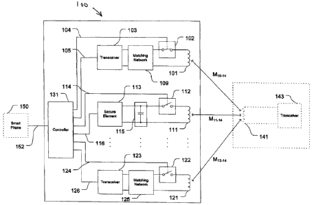
An embodiment of a multi-mode adapter according to one embodiment of the
invention is shown at 100 in FIG. 2. In this embodiment, controller 131 is a
Texas
Instruments MSP430 microcontroller with digital general purpose output pins.
Other
microprocessors and dedicated controllers known in the art are also suitable
for this
function. In one embodiment, antenna 101 is an electromagnetic near-field loop
antenna.
Other antennas known in the art are also suitable for this function. In one
embodiment,
transceiver 103 is a Texas Instruments TRF7970A NFC and radio frequency
identification reader and writer (NFC/RFID Reader Writer) IC. Matching network
109 in
one embodiment is an RF matching network known in the art having two filter
networks
as described above.
In one embodiment, switches 102 and 122 are CEL uPG2406TK Gallium
Arsenide switches and switch 112 is a CEL uPG2189 Gallium Arsenide switch.
Other
8
CA 02819006 2013-05-24
WO 2012/069918
PCT/1B2011/002818
switches known in the art are also suitable. Switch 102 is preferably
positioned between
antenna 101 and transceiver 103 to connect them when the switch 102 is closed,
and to
disconnect them when the switch 102 is open. Control line 104 connects one of
the
general purpose outputs of controller 131 to the control pin of switch 102 to
control the
switching state of said switch.
In one embodiment, controller 131 is connected to NFC/RFID Reader Writer 103
via an SPI interface 105, or other suitable interface such as parallel general
purpose I/0
bus. Controller 131 is connected to a mobile phone 150, e.g., a host mobile
phone, smart
phone, or tablet computer. In one embodiment, controller 131 is connected to
mobile
phone 150 via a UART interface 152, or other suitable interface such as USB.
In one embodiment, antenna 111 is an electromagnetic near-field loop antenna.
Other antennas known in the art are also suitable for this function. In one
embodiment,
near field device 113 is a NXP P5CD072 secure element module with a
GlobalPlatform
compliant operating system and a credit card payment application loaded into
internal
EEPROM memory. Other suitable secure elements having a contactless interface
for
connection to an antenna are known in the art. Attached to the output pins of
said secure
element 113 is a resonating capacitor 115. In one embodiment, switch 112 is
positioned
in the path between antenna 111 and smart element 113, to connect them when
the switch
is closed, and disconnect them when the switch is open. Control line 114
connects one of
the general purpose outputs of controller 131 with the control pin of switch
112. In one
embodiment, controller 131 is connected to smart element 113 via ISO 7816
interface
116, or other suitable interface that may be supported by the smart element,
such as USB.
In one embodiment, antenna 121 is an electromagnetic near-field loop antenna.
Other antennas known in the art are also suitable for this function. In one
embodiment,
near field device 123 is a Sony Felica RC-S860 contactless smart card IC
transceiver,
with a transit fare payment application loaded into its memory. Other suitable
RFID tags,
including an NXP Semiconductor MF3MOD4101DA4/04 DESFire Smart Card IC are
useable as near field device 123. Attached to the output pins of near field
device 123 is a
matching network 125, which in one embodiment is a second resonating
capacitor.
Switch 122 is positioned in the path between antenna 121 and near field device
123, to
9
CA 02819006 2013-05-24
WO 2012/069918
PCT/1B2011/002818
connect them when the switch is closed, and disconnect them when the switch is
open.
Control line 124 connects one of the general purpose outputs of controller 131
with the
control pin of switch 122.
During operation of system 100, the exemplary external near field device to
which system 100 communicates is shown in phantom at 143 with its associated
antenna
141.
FIG. 3 is a flow chart of a method for operating a multi-mode communication
system for a mobile phone according to one embodiment of the invention. As
seen in
FIG. 3, a method according to one embodiment for operating a multi-mode mobile
communication system is shown at 200 and includes determining, as shown at 202
which
of 1-N modes of operation is to be performed by said system. In one
embodiment, as
shown at 204, 206 and 208, once one of said modes of operation is selected,
all of the
switches in the system that connect the respective near field devices to their
respective
antennas are opened. For each mode of operation selected, as seen at 210, 212,
and 214,
the system causes those switches to close to enable the selected near field
device and
antenna to perform the selected mode of operation. Lastly, the method detects
when to
end the selected mode of operation, as seen at 216, 218, and 220.
Exemplary modes of operation of the multi-mode communication system
according to the invention are as follows:
I. Contactless Payment Mode of Operation (Mode 1)
Controller 131 opens all switches, for break-before-make transition between
modes, then closes switch 112, connecting antenna 111 to near field device
(secure
element) 113 and resonating capacitor 115, thereby enabling a contactless
credit card
payment transaction with an external contactless payment reader, represented
by the
transceiver 143 and antenna 141, shown in phantom in Figure 2, by magnetic
field
induction employing mutual coupling Mi i -14 between antennas 111 and 141.
Controller
131 coordinates and controls secure element 113 via an ISO 7816 interface
during
contactless transactions between secure element 113 and external Point-of-Sale
contactless terminal. Controller 131 interacts with a User Interface software
application
on host smart phone 150.
CA 02819006 2013-05-24
WO 2012/069918
PCT/1B2011/002818
II. Two-way NFC Mode of Operation (Mode 2)
Controller 131 opens all switches, for break-before-make transition between
modes, then closes switch 102, thereby connecting antenna 101 to near field
device 103,
an NFC transceiver, and enabling two way NFC communication with an external
NFC
device, represented by the transceiver 143 and antenna 141, shown in phantom
in Figure
2, by magnetic field induction employing mutual coupling M10-14 between
antennas 101
and 141. With switch 112 open, secure element 113 and resonating capacitor 115
are
disconnected from the antenna 111, breaking that circuit loop. Thus, secure
element 113
and resonating capacitor 115 are de-coupled from, and do not present a coupled
load to,
any circuit connected to antenna 101. Controller 131 coordinates and controls
NFC/RFID transceiver 103 via SPI interface 105 during RFID read/write of
external
RFID tag (not shown in Fig. 1) in field. Controller 131 interacts with a User
Interface
software application on host smart phone 150.
III. RFID Reader Mode of Operation (Mode 3)
Controller 131 opens all switches, for break-before-make transition between
modes, then closes switch 102, connecting antenna 101 to transceiver 103,
thereby
enabling radio frequency identification read of external radio frequency
identification tag,
represented by the module 143 and antenna 141, shown in phantom in Figure 2,
by
magnetic field induction employing mutual coupling M10.14 between antennas 102
and
141.
IV. RFID Writer Mode of Operation (Mode 4)
Controller 131 opens all switches, for break-before-make transition between
modes, then closes switch 102, connecting antenna 101 to transceiver 103,
thereby
enabling radio frequency identification write of external radio frequency
identification
tag, represented by the module 143 and antenna 141, shown in phantom in Figure
2, by
magnetic field induction employing mutual coupling M10-14 between antennas 102
and
141.
V. Transit Fare Mode of Operation (Mode 5)
11
CA 02819006 2013-05-24
WO 2012/069918
PCT/1B2011/002818
Controller 131 opens all switches, for break-before-make transition between
modes, then closes switch 122, connecting antenna 121 to transceiver 123,
thereby
enabling transit fare payment with external transit system reader, represented
by the
module 143 and antenna 141, shown in phantom in Figure 2, by magnetic field
induction
employing mutual coupling M12-14 between antennas 122 and 141.
FIG. 4 is a functional block diagram and schematic of a multi-mode
communication system for a mobile phone according to a second embodiment of
the
invention. As seen in FIG. 4, the multi-mode communication system 800 includes
first
and second antennas 801 and 811. A matching network 809 is connected to first
antenna
801. A resonant capacitor 815 is connected to the second antenna 811. A first
near field
device 803 is connected to matching network 809. In one embodiment, first near
field
device 803 is a conventional NFC/RFID transceiver IC. A second near field
device 813
is connected to a second matching network comprising a resonant capacitor 815.
In one
embodiment, second near field device 813 is a conventional secure element. A
first
switch 802 is connected between matching network 809 and first antenna 801 and
a
second switch 812 is connected between resonant capacitor 815 and second
antenna 811.
A controller 831 controls the switched state of said first and second switches
802, 812 via
respective control lines 804 and 814 such that only one of said near field
devices 803,
813 is selectively coupled to its respective antenna at any given time.
Controller also is
connected to near field devices 803, 813 by respective bus lines 805 and 816.
Communication between the host mobile phone 850 and controller 831 is by bus
line
852. During operation of system 800, the exemplary external near field device
to which
system 800 communicates is shown in phantom at 843 with its associated antenna
841.
Note in the embodiment shown in FIG. 4, the multimode communication system
800 is external to mobile phone 850. As illustrated in FIG. 9, any embodiment
of
multimode communication system according to the invention can also be embedded
in
the mobile phone.
FIG. 5 is a partially exploded perspective view of an adaptor incorporating a
multi-mode communication system for a smart phone having a shape that enables
it to be
attached as a sleeve to the mobile phone according to one embodiment of the
invention.
FIG. 6 is a partially exploded perspective view of the adaptor of FIG. 5
showing the
12
CA 02819006 2013-05-24
WO 2012/069918
PCT/1B2011/002818
position of various components of the adaptor according to one embodiment of
the
invention. FIGS. 5 and 6 show the device in a sleeve/cradle/sled industrial
design or
form factor such as an adaptor for an iPhone 4 smart phone. The device is
similar
industrial design of form-factor could be customized for other smart phones,
mobile
phones, and tablets.
As seen in FIG. 5, in one embodiment of the system of the invention, the
system
is formed in the shape of an adaptor 600 having a top 602 and a bottom 604
that, when
joined together, securely fit around a mobile phone 606. As seen in FIG. 6,
adaptor 600
includes a printed circuit board (PCB) 608, a ferrite sheet 610 and an inner
plastic sheet
612 that fit together in bottom 604 of adaptor 600 in such a fashion that they
do not
obstruct the sliding of bottom 604 around mobile phone 606.
The various circuit elements of the system of the invention, as described
above
with respect to FIGS 2 and 3 and as will be described below in FIGS. 7-9 are
all mounted
on PCB 608. Ferrite sheet 610 is for isolating the antennas formed on PCB 608
from the
mobile phone 606. Inner plastic sheet 612 is to cover the PCB 608 and ferrite
sheet610.
As is also seen in FIG. 6, inner plastic sheet 612 includes a connector 614
for enabling
the system of the invention to be connected to the mobile phone 606's
conventional data
interface plug.
FIG. 7 is a top view of an exemplary printed circuit board 608 that contains
components of the multi-mode communication system according to the present
invention
and FIG. 8 is a bottom view of the exemplary printed circuit 608 shown in FIG.
7. As
seen in FIG. 6, PCB 608 includes switches 502 and 512, an NFC/RFID transceiver
503
and its matching network 509, secure element 513 and its resonating capacitor
515, and
controller 531. Also shown in FIG. 7 is the placement of the ferrite sheet 570
on the
surface of PCB 608. As seen in FIG. 8, the bottom side of PCB 608, the ferrite
sheet
footprint matches the footprint area taken up by antennas 601 and 611, to
shield these
antennas from the adjacent mobile phone when adaptor 600 is jacketing the
mobile
phone. Note that antenna 601, for the NFC/RFID transceiver has thicker traces
than the
antenna 611 used by the secure element. As described above, this is because
there is a
13
CA 02819006 2013-05-24
WO 2012/069918
PCT/1B2011/002818
greater amount of current that antenna 601 has going through it when the
NFC/RFID
transceiver is operating.
FIG. 9 is a functional block diagram and schematic of a multi-mode
communication system 900 for a mobile phone according to a third embodiment of
the
invention. In FIG. 9, components corresponding to the components shown in FIG.
4 have
the same numbers. As seen in FIG. 9, system 900 is embedded in mobile phone
950
rather than external to the mobile phone, as seen in FIG. 4. Mobile phone 950
includes
smart phone electronics 935 to which system 900 is coupled.
As also seen in FIG. 9, in this embodiment a voltage generator 965 is included
in
system 900. Voltage generation 965 is connected to antenna 801 via line 960
and
functions to generate a voltage from antenna 801 by magnetic induction from a
magnetic
field when mobile phone 950 is positioned in an area where such a field is
being
generated by an external device. Voltage generator 965 provides sufficient
power to
enable the connection of said secure element and resonant capacitor to said
second
antenna, thus enabling secure element transactions even when the mobile phone
950 is
off.
In one embodiment, the output of voltage generator 965 is connected to switch
812 and to first and second default control circuits 985 and 975 as well as to
a field detect
input of controlled 931. In operation, when an external magnetic field is
sufficient to
generate a voltage on line 970 via generator 965, the first and second default
control
circuits are powered up and operate to disconnect switch 802 via line 990 and
connect
switch 812 via line 980.
As is seen, by using multiple antennas, the invention allows for the circuit
network topology, antenna size, antenna shape, number and antenna windings,
antenna
inductance, Q-factor, and frequency response tuning to be individually
optimized for
each RFID transceiver IC, smart element, and RFID tag function in the
invention. This is
an advantage over the prior art, which must compromise its single antenna and
circuit
network for the divergent requirements of RFID transceiver and load-modulated
NFC
functions. As a result, the invention's multiple antennas achieve longer range
and better
performance than the prior art. The invention can accommodate RFID
transceivers,
14
CA 02819006 2016-11-01
smart elements, and RFID tags not originally designed for NFC. The invention
is not
dependant on, nor limited to, smart elements with 12S, SWP, and microSD
interfaces.
The invention can be easily and flexibly scaled to a multiplicity of
transceivers,
multiplicity of smart elements, and multiplicity of RFID tags in a single
device, each with
its own antenna and switches. The invention can accommodate arbitrary
combinations of
RFID transceivers, smart elements, and RFID tags. Thereby, the invention can
incorporate combinations of multiple contactless protocols, for example ISO
15693 in
combination with Felicia, that are not available in a single smart element or
RFID tag.
The present invention has been described in relation to particular examples,
which
are intended in all respects to be illustrative rather than restrictive. Those
skilled in the
art will appreciate that many different combinations of circuits will be
suitable for
practicing the present invention. Moreover, other implementations of the
invention will
be apparent to those skilled in the art from consideration of the
specification and practice
of the invention disclosed herein. It is intended that the specification and
examples
therein be considered as exemplary only. The scope of the claims should not be
limited
by the preferred embodiments set forth in the examples, but should be given
the
broadest interpretation consistent with the description as a whole.