Note: Descriptions are shown in the official language in which they were submitted.
81771198
MAKING SEMICONDUCTOR BODIES FROM MOLTEN MATERIAL USING A FREE-
STANDING INTERPOSER SHEET
[0001] This claims
priority to U.S. Provisional application
No. 61/418,699, THIN CERAMIC BODIES FOR USE MAKING THIN
SEMICONDUCTOR BODIES FROM MOLTEN MATERIAL AND METHODS OF USING
SUCH CERAMIC BODIES, filed in the names of Emanuel M. Sachs
and Ralf Jonczyk, on December 1, 2010.
-1-
CA 2819144 2018-06-11
CA 02819144 2013-05-27
WO 2012/075306
PCT/US2011/062914
[0002] The Direct Wafer application describes a method of
making semi-conductor bodies, for instance wafers for use as
solar cells, directly from a melt of semiconductor material.
The following discussion is taken in part from the Direct
Wafer application, with some modifications. An aspect of a
Direct Wafer process will first be discussed in a batch
implementation, where a single semiconductor sheet is made at
a time, as shown schematically with reference to Figs. 1, 2
and 3A-3D. A semiconductor melt 13 may be contained in a
crucible 11 made of graphite, silica, silicon carbide, silicon
nitride and other materials capable of containing molten
semiconductor, such as silicon. The processes disclosed
herein are suitable for fabrication of many different types of
semiconductor material. Silicon will be discussed as
representative, but the inventions are not intended to be
limited to use with only silicon.
[0003] As shown in Fig. 1 a vacuum plenum 1 is created, for
example, by machining a cavity 3 into a block of graphite. A
thin sheet 5 of, graphite or other suitable material, is
affixed to the bottom of the plenum 1. This sheet preferably
has a fair degree of gas permeability (having a high porosity
and/or being relatively thin). The plenum is preferably the
least porous graphite (or other suitable material) available.
The plenum could also be made of non-porous ceramic. The thin
sheet 5 will be referred to herein as the mold sheet. Vacuum
suction is applied at port 7. Referring now to Fig. 3A, the
assembly 8 is brought into contact with the surface 15 of melt
13. The assembly remains in contact with the melt for a
designated period of time, perhaps on the order of 1 second.
The amount of contact time between the assembly and the melt
will vary depending on factors that include, but are not
limited to: the temperature of the melt, the temperature of
the mold sheet, the thickness of the mold sheet and the
intended thickness of the silicon sheet to be fabricated. A
silicon sheet freezes onto the mold sheet, as shown in Fig.
3B. The process is thus a transient heat transfer resulting
-2-
ak 02819144 2013-05-27
WO 2012/075306
PCT/US2011/062914
in the silicon melt 13 being cooled to the melting point and
then heat of fusion being extracted, resulting in the buildup
19 of solid silicon on the mold sheet. In general, at least a
portion of the mold sheet should be at a temperature below the
freezing point, for at least a portion of the time that the
mold sheet contacts the molten material. Taking silicon as an
example, the freezing/melting point is 1412 C). Useful ranges
for maintaining the mold sheet for use with silicon as the
semiconductor might go from room temperature to any
temperature below the freezing/melting point.
[0004] A principal purpose of the vacuum is to cause the
formed silicon sheet 19 to be temporarily held against the
mold sheet 5. It is helpful that the silicon sheet 19 be
easily removed from the mold sheet 5 after the silicon sheet
is formed. It is very helpful if the silicon sheet would
simply fall off. However, it is very important that as the
silicon sheet is being formed, it adhere to the mold sheet 5.
The vacuum 17 accomplishes this goal. Without the vacuum,
when the mold sheet is removed after being in contact with the
molten silicon 13 for the appropriate length of time, the
solidified silicon 19 would likely remain behind on the top 15
of the melt and then it would re-melt. Indeed, significant
adhesion is needed to remove the solidified silicon sheet 19
from the melt 13 because the surface tension of the molten
silicon is holding the silicon sheet 19 down.
[0005] After the designated period of time, the assembly 8
is lifted out of the melt 13, now carrying silicon sheet 19
attached to it, as shown in Fig. 3C. Finally, in Fig. 3D, the
vacuum 17 is released and the formed silicon sheet 19 can be
separated from the mold sheet 5. Upon release of the vacuum 17
the silicon sheet 19 may simply fall off. However, some small
amount of residual adhesion may keep the sheet from falling
off.
-3-
CA 02819144 2013-05-27
WO 2012/075306
PCT/US2011/062914
[0006] The graphite mold sheet 5 must have sufficient
porosity to allow for suction sufficient to accomplish the
goal of adhering to the silicon sheet 19. There are a very
large variety of grades of graphite, ranging over a very large
range of porosity. Thus there are many suitable choices.
[0007] The porosity of the mold sheet 5 must not be so
great as to allow the molten silicon 13 to enter the pores,
thereby making release of the silicon sheet 19 difficult or
impossible. Two independent factors combine to prevent
silicon from entering into fine pores. First, the surface
tension of the molten silicon is too high to permit it to
infiltrate fine pores (of a non-wetting material). Second,
the silicon is beginning to freeze rapidly on contact to the
mold sheet and this freezing would be especially fast in the
high surface area to volume ratio situation presented by a
fine pore. The second factor is present even for a wetted
material.
[0008] The foregoing discussion relates to using a melt
surface at approximately atmospheric pressure. It is also
possible, and discussed in the Direct Wafer applications to
use a melt surface at higher than atmospheric pressure.
[0009] The interface between the forming surface and the
molten semiconductor and later, solidified wafer is very
important. It is advantageous for this forming interface to
separate cleanly upon reduction of the vacuum being applied
through the mold sheet. Further, it is helpful if it allows
for some slipping between the wafer and the mold sheet,
especially as the wafer cools and shrinks differently than the
mold sheet. It is also advantageous for the forming interface
to allow for the growth of large grains by avoiding the rapid
nucleation of a high multiplicity of grains. To accomplish
this, the interface can be of a nature to allow under-cooling
of the melt, while maintaining a low propensity to nucleate
grains, for example, by providing at this interface a material
-4-
CA 02819144 2013-05-27
WO 2012/075306 PCT/US2011/062914
with a low propensity to nucleate grains. Further, it is
useful to control the heat transfer across this interface to
exercise influence over the grain size formed in the
semiconductor wafer. For example, reducing the heat flow
across the interface can allow time for nucleated grains to
grow laterally, thus resulting in larger grain sizes. The
nature of this interface should be created and modified in a
well-controlled manner so that successive wafers formed have
similar properties. The nature of this forming interface
should also be controlled in an economical manner that can be
implemented in a realistic production environment
SUMMARY OF INVENTIONS
[0010] Method inventions disclosed herein employ a sheet
referred to herein as an interposer sheet for use making
semiconductor bodies, such as of silicon, such as for solar
cell use. It is free-standing, very thin, flexible, porous and
able to withstand the chemical and thermal environment of
molten semiconductor, such as silicon, without significant
degradation. It is typically of a ceramic material, such as
silica, silicon nitride, silicon oxynitride, silicon
oxycarbide, silicon carbide, silicon carbonitride, silicon
oxycarbonitride and others, as discussed below. It is provided
between the forming surface of a mold sheet, and the molten
material from which a semiconductor body will be formed. It
may be either secured to the head structure that carries the
mold sheet with its forming surface or deposited upon the
surface of the melt. The composition of the interposer sheet
helps to suppress grain nucleation, leading to relatively
large grain sizes. It also helps to limit heat flow from the
melt, which controls the timing of solidification of the
semiconductor body. It also promotes separation of the
solidified semiconductor body from the forming surface.
Because it is free standing, it can be fabricated before its
use, and therefore, its properties can be tested and verified,
leading to a high degree of reliability and reproducibility
-5-
81771198
from one solidified body to the next. Also, using a
freestanding interposer sheet permits greater control over the
factors mentioned in this paragraph, than can be had with
particulate, or other non-free-standing articles for achieving
similar functions. An interposer sheet itself is also an
invention hereof. Because it is free-standing and not adhered
to the forming surface, problems of mismatch of coefficients of
thermal expansion either are minimized or do not arise, because
the interposer sheet and the solidified semiconductor body are
free to expand and contract relatively independently of the
forming surface. Further, the formed semiconductor body is
relatively free to release from its association with the
forming surface, because the interposer sheet prevents
adherence of the semiconductor body to the forming surface.
[0010a] According to one aspect of the present invention,
there is provided a method for fabricating a semi-conductor
body, the method comprising the steps of: a. providing a molten
semi-conductor material, having a surface; b. providing a
porous mold, comprising a forming surface; c. providing a free-
standing ceramic sheet between the forming surface and the
molten material; d. contacting the forming surface to the
ceramic sheet and the ceramic sheet to the surface of the
molten material for a contact duration, such that a body of
semiconductor material, solidifies upon the ceramic sheet; and
e. removing the solidified body from contact with the molten
semi-conductor material while still contacting the ceramic
sheet.
[0010b] According to another aspect of the present invention,
there is provided an assembly comprising: a. a porous mold,
comprising a forming surface; b. a free-standing porous
- 6 -
CA 2819144 2018-06-11
81771198
refractory ceramic sheet having a first and second surface,
being secured at the first surface to the forming surface of
the mold; c. secured to the second surface of the ceramic
sheet, a semiconductor body formed directly from a molten
quantity of semiconductor material.
[0010c] According to still another aspect of the present
invention, there is provided an apparatus for fabricating a
semiconductor body from a molten supply of semiconductor
material, the apparatus comprising: a. a porous mold,
comprising a forming surface; b. a holding mechanism configured
to hold a free-standing ceramic sheet facing the forming
surface, such that the ceramic sheet hangs away from the
forming surface such that the ceramic sheet can contact a
surface of molten material at a contact location and such that
the forming surface, can be brought to contact the ceramic
sheet obverse of the contact location; and c. a structure
configured to provide a differential pressure regime such that
pressure at the contact location is less than pressure at the
surface of molten material.
BRIEF DESCRIPTION OF THE FIGURES OF THE DRAWING
[0011] Fig. 1 is a schematic representation of a known plenum
and refractory mold sheet for use with inventions hereof;
[0012] Fig. 2 is a schematic representation of such a known
plenum with a refractory mold sheet 35 having a textured
surface 9;
[0013] Figs. 3A, 3B, 3C and 3D are a schematic representation
of known method steps using a plenum such as shown in Fig. 1,
with:
- 6a -
CA 2819144 2018-06-11
' 81771198
[0014] Fig. 3A showing a refractory mold sheet contacting a
melt surface;
[0015] Fig. 38 showing a body of semiconductor formed on the
mold sheet;
[0016] Fig. 3C showing the plenum and mold sheet assembly
removed from the melt; and
- 6b -
CA 2819144 2018-06-11
CA 02819144 2013-05-27
WO 2012/075306
PCT/US2011/062914
[0017] Fig. 3D showing the formed semiconductor body
released from the mold sheet upon release of the vacuum in the
plenum;
[0018] Figs. 4A-4G show, schematically, a sequence of steps
using an interposer sheet of an invention hereof, secured to a
mold sheet, by clamping at its edges, as the mold sheet
advances toward the molten material, with:
[0019] Fig. 4A showing an interposer sheet secured to a
forming surface with its center hanging and spaced away from
that of the forming surface;
[0020] Fig. 4B showing the interposer sheet first
contacting the molten surface;
[0021] Fig. 40 showing the interposer sheet contacting the
molten surface over the entire sheet area;
[0022] Fig. 4D showing the forming surface contacting the
back surface of the interposer sheet, away from the molten
surface;
[0023] Fig. 4E showing a semiconductor body forming on the
interposer sheet;
[0024] Fig. 4F showing the mold sheet and forming surface
lifted away from the molten material, carrying the solidified
semiconductor body on the interposer sheet; and
[0025] Fig. 4G showing the interposer sheet separated from
the forming surface, still carrying the solidified
semiconductor body;
[0026] Figs. 5A-5D show, schematically, a sequence of steps
using an interposer sheet of an invention hereof, secured to a
mold sheet, by means not shown, for use with a crucible having
one wall that is relatively lower than another wall, as the
mold sheet advances toward the molten material, with:
-7-
CA 02819144 2013-05-27
WO 2012/075306 PCT/US2011/062914
[0027] Fig. 5A showing an interposer sheet secured to and
contacting a forming surface substantially over its full
extent;
[0028] Fig. 5B showing the interposer sheet first
contacting the molten surface at a meniscus above the
relatively lower wall;
[0029] Fig. 5C showing the interposer sheet and mold sheet
advanced further along a direction of arrow M, with a
significant extent of semiconductor solidified upon the
interposer sheet; and
[0030] Fig. 5D showing a fully formed semiconductor body
upon the interposer sheet, and the crucible moved away from
the mold sheet assembly;
[0031] Figs. 6A-6C show, schematically digital images of
photomicrographs, depicting a range of porosity and
configuration of pores and solid grounds of an interposer
sheet of an invention hereof, with:
[0032] Fig. 6A showing a least porous interposer sheet;
[0033] Fig. 6B showing a moderately porous interposer
sheet; and
[0034] Fig. 6C showing a more porous interposer sheet.
DETAILED DESCRIPTION
[0035] Materials to achieve various functions, important to
the forming interface, such as to reduce nucleation, control
grain growth and to affect heat flow, among other functions,
can be provided in the form of a free-standing sheet of
suitable material, including, but not limited to: silica,
silicon nitride, silicon oxynitride, silicon oxycarbide,
silicon carbide, silicon carbonitride, silicon oxycarbonitride
and others, and others. Others may include alumina, mullite,
-8-
CA 02819144 2013-05-27
WO 2012/075306
PCT/US2011/062914
and boron nitride. In general, any ceramic that can withstand
the temperatures without degrading may be used. Ceramics that
contain materials that may be deleterious to formation of
semiconductor bodies, such as alumina, mullite and boron
nitride may be used, if the conditions are such that no
significant amount of such deleterious material exits the
ceramic and enters the semiconductor body. Such a sheet is
referred to herein as an interposer sheet.
[0036] By free-standing, it is meant a body that is
fabricated some time before its intended use, and is capable
of being handled separately, without being secured to a larger
or more massive or stiffer substrate. A free-standing body may
have a relatively thin sheet on one or more surfaces, and may
also carry upon one or more surfaces other incidental small
elements, such as local coatings, seeds, etc.
[0037] Such an interposer sheet of material is fabricated
in a separate operation, at an earlier time, and this
interposer sheet is then used to make semiconductor bodies,
such as wafers, by methods similar to those disclosed in the
incorporated Direct Wafer patent application, but augmented
with use of one or more interposer sheets, as discussed
herein. Such sheets may be referred to herein as an interposer
sheet, or in some cases, simply, as a sheet. A typical
semiconductor body that may be formed with these methods is a
wafer of silicon for use in solar cells. However, other
semiconductors, and other bodies may also be formed.
[0038] As shown in Fig. 4A an interposer sheet may be
provided between the forming surface 46 of the mold sheet 45
and the surface 415 of the molten material 413. It may be
provided secured to the mold sheet, as shown with reference to
Figs. 4A-4G, for an embodiment that is clamped, and hangs (as
discussed below); or as shown in Figs. 5A-5D, for an
embodiment that is secured more tightly over its extent; or
may be deposited upon the molten surface 415 (un-shown).
-9-
CA 02819144 2013-05-27
WO 2012/075306 PCT/US2011/062914
[0039] The interposer sheet is porous, to allow the
pressure differential, such as a vacuum of the wafer forming
method disclosed in the Direct Wafer patent application, to
propagate through the interposer sheet to the molten silicon.
The degree of porosity of the interposer sheet can vary widely
from just 1 percent to as high as approximately 80%. The
diameter of the openings can vary from a 1 micron to up to
approximately 100 microns. Even an opening of as large as
approximately 100 microns will not admit the molten silicon to
contact the forming face 46 of the porous mold sheet 45. This
is especially so because the materials used for an interposer
sheet that is designed to provide for only minimal grain
nucleation are also not well wetted by the molten silicon. It
is advantageous that at least a moderate fraction of the
porosity be open porosity, to allow the vacuum to be conducted
through the mold sheet and the interposer sheet. It is also
possible for all the porosity to be open. Some degree of
closed cell porosity may be present.
[0040] Figs. 6A-6C illustrate a range of porosity and
configurations of the pores and solid ground. Fig. 6A shows a
relatively less porous interposer sheet, as compared to the
others shown. Fig. 6B shows a moderately porous interposer
sheet, and Fig. 6C shows a more porous interposer sheet.
[0041] In this document, when a sheet thickness is stated
it will be the mass-equivalent sheet thickness, or ME
thickness. That is, a porous sheet of ME thickness 5 microns
has a mass equivalent to that of a 5 micron thick, fully dense
sheet of the same area and made of the same material. For
example, If the porosity of the sheet is 50%, and the ME
thickness is 5 microns, then the thickness extent (from
tallest peak on one surface to the tallest peak on the obverse
surface) of the sheet is at least 10 microns. Typically, the
free-standing interposer sheet has a ME thickness of between 1
and 10 microns, with a preferred range of 2 to 5 microns.
-10-
CA 02819144 2013-05-27
WO 2012/075306
PCT/US2011/062914
[0042] Preferably, the interposer sheet has a significant
degree of flexibility, owing to its thin and porous nature.
This flexibility facilitates handling and clamping of the
interposer sheet and serves purposes using the interposer
sheet, including allowing the interposer sheet to conform well
to the forming surface of the mold sheet and the surface of
the liquid melt and, in some modes, allowing the interposer
sheet to take on a deliberate curvature as described below. In
some embodiments, the sheet should be able to assume a radius
of curvature as small as 2 mm. For instance, as shown in Fig.
4A, the clamp 434 secures an interposer sheet 430 that assumes
a curvature having a radius of about 2 mm. In some cases, a
minimum degree of flexibility is not critical. Due to the
thinness of the interposer sheet for other purposes, it will
inherently be thin enough to conform to the forming surface
shape, or non-level regions of a molten surface. However, for
some purposes, such as the clamping shown above, a high degree
of flexibility may be important and very beneficial.
[0043] As shown schematically with reference to Figs. 5A ¨
5D, discussed more fully below, an interposer sheet 530 may be
adhered to the porous mold sheet 55, for example, using the
vacuum drawn through the porous mold sheet 55. Alternatively,
as shown schematically with reference to Figs. 4A-4C, an
interposer sheet 430 may be supported from the mold sheet 45,
or from the head 41 that holds the mold sheet 45, by clamping
at its edges with clamps 434. Clamping and a secondary means
of attachment, such as vacuum 47, may be used simultaneously.
Depending on the selected ceramic material the interposer
sheet could be electrically charged and that charge could be
used to attach the interposer sheet to the forming surface of
the mold sheet. Such electrostatic attachment of the
interposer sheet to the mold sheet can also be accomplished by
establishing a voltage on the mold sheet.
[0044] The mold sheet with an interposer sheet attached is
lowered into the melt, vacuum is drawn and a semiconductor
-11-
CA 02819144 2013-05-27
W02012/075306
PCT/US2011/062014
wafer sheet is solidified. The mold sheet and solidified
semiconductor sheet can be removed from the melt in a variety
of manners similar to those described in the Direct Wafer
application, but augmented significantly by the presence of an
interposer sheet. The vacuum
can be initiated before the
interposer sheet contacts the melt or after contacting the
melt.
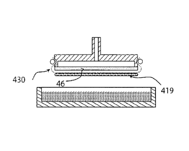
[0045] As shown with reference to Fig. 4A when the porous
sheet 430 is supported from the mold sheet 45 by its edges,
the interposer sheet 430 may be allowed to hang down. In
this way, as shown in Fig. 4B, the free center 432 of the
interposer sheet 430 initially contacts the surface 415 of the
melt while free of the forming surface 46 of the porous mold
sheet 45. The mold sheet 45 continues to descend and then as
shown in Figs. 40 and 4D, presses upon the back surface 433 of
the interposer sheet 430, and then reaches the level of the
surface 415 of the melt 413. This allows the interposer sheet
430 time to warm up and be wetted by the melt 413 before the
contact of the forming surface 46 of the mold sheet 45 to the
back surface 433 of the interposer sheet. For example with a
porous mold sheet 45 of 160 x 160 mm, the interposer sheet 430
may be clamped at two edges such that the center 432 of the
interposer sheet hangs down from the forming surface 46 by
approximately 10 mm. This requires that the interposer sheet
be able to assume a radius of curvature of about 325 mm or
smaller. An interposer sheet that can assume a radius of
curvature of approximately 150 mm can be handled with a wide
variety of configurations. With an even higher degree of
flexibility, such as being able to assume a curvature having a
radius of about 2-3 mm, an interposer sheet can be clamped by
a small diameter clamp such as shown at 434 in Fig. 4A-4G.
[0046] In another embodiment, not shown in a separate
figure, the interposer sheet may be placed on the surface of
the molten silicon independent of the mold sheet and
sufficient time allowed for the interposer sheet to be wetted
-12-
CA 02819144 2013-05-27
WO 2012/075306 PCT/US2011/062914
(typically a few seconds). The mechanism that can place the
interposer sheet can be similar to that shown in Fig. 4A at
434, except that the mating element of the clamp 434 is not
the head 41 that holds the mold sheet 46. Rather, it can be a
separate element, typically part of a larger frame, having an
open region large enough for the entire head 41 and mold sheet
46 assembly to fit through the opening to contact the back
side 433 of the interposer sheet 430, once deposited upon the
molten surface 415. But the mechanical function would be the
same namely to mate with the clamp 434 to hold the interposer
sheet 430 as it is brought near to the surface of the melt,
and then contacts the melt, and also optionally to secure it
in position while on the melt. The porous forming surface can
then be lowered down onto the wetted interposer sheet, through
the opening in the frame, and then all can be drawn away from
the melt together. It has been found that pre-wetting of the
interposer sheet can result in larger grain sizes, as is
desirable.
[0047] Other apparatus and methods of placing the
interposer sheet upon the melt before the forming surface
contacts the back of the interposer sheet can be used. It will
likely be important to have a mechanism that can release the
interposer sheet from its grasp, and then ensure that the
deposited interposer sheet either remains in a position or
undergoes controlled motion so that the mold sheet can be
reliably brought to bear upon it. The interposer sheet can be
applied to the melt so that it first contacts the melt at a
region near its center, such as shown at 432 of Fig. 4B, which
is a generally a line. The contact region may be a line, such
as parallel to an edge or diagonal of the sheet, or a very
small region.
[0048] Whether the interposer sheet is deposited by a
dedicated purpose depositing device, or as clamped to the head
41 that also holds the mold sheet 45, one method of making
wafers using an interposer sheet is to place the interposer
-13-
CA 02819144 2013-05-27
WO 2012/075306
PCT/US2011/062914
sheet on the melt surface between approximately 0.1s and
approximately 5s before the forming surface engages the back
surface of the interposer sheet, facing away from the melt.
[0049] As shown in Fig. 4E, the forming surface 46 is under
vacuum 47 or differential pressure less than that of the melt
surface and, nucleates a relatively low number of grains in
the under-cooled silicon 434 contacting the interposer sheet
430. (An under-cooled liquid remains liquid even at a
temperature that is below its melting temperature.) Depending
on subsequent dwell-time in the melt, the forming surface
temperature, vacuum level and mold sheet thermal properties, a
semiconductor body 419, such as a wafer of desired thickness
with large grains (up to 10mm have been observed) is grown.
[0050] It is then, as shown in Fig. 4F, removed from the
melt 413. Aspect ratios of up to 50:1 for grain size and
thickness have been observed with the grain size 50 times the
thickness of the wafer. The wafer is coupled to the mold sheet
forming surface 46 with the interposer sheet 430 interposed
between the two, by a vacuum 47. There is little to no
chemical or mechanical interaction of the formed wafer body
419 with the forming surface 46. They are not contacting each
other.
[0051] As shown in Fig. 4G, the interposer sheet 430 is
moved away from and becomes separated from the forming surface
46, with the formed semiconductor body 419 still associated
with the interposer sheet 430, by reducing or removing the
vacuum pressure 47. The interposer sheet 430 is then
separated from the solidified body 419, as discussed below,
typically in a separate, later process.
[0052] Another arrangement for using an interposer sheet is
shown schematically with reference to Figs. 5A-5D. A
crucible, 511 has at least one side that is relatively lower
542 than the others. The molten material is provided to a
depth such that a meniscus 515 resides above the level of the
-14-
CA 02819144 2013-05-27
WO 2012/075306
PCT/US2011/062914
lower wall 542. The lower wall may extend across the entire
width of the crucible (in a dimension into the page), or it
may occupy only a partial region of such a width, with higher
wall portions at the corners. The walls of the crucible not
shown, due to the section, may be slanted, from low at the
corner with the lower wall 542, or may be fully higher. The
mold sheet 55 is part of a head assembly 51, which can be
moved in the direction of the arrow M (to the left as shown)
toward and along the crucible 511. An interposer sheet 530 is
secured to the forming surface of the mold sheet 55 by means
not shown, but also including suction action from a
differential pressure 57, such as a vacuum, as discussed
above. As the head assembly 51 is moved in the direction of
the arrow M, the crucible 511 may typically be moved to meet
it, in the direction of the arrow C. This mutual motion helps
to minimize irregularities in the formed wafer at the location
of initial contact.
[0053] Fig. 5B shows, schematically the molten liquid 513
being drawn toward the mold sheet 55, and also along in the
direction of the arrow M. The molten material directly
contacts the interposer sheet 530, and does not contact the
mold sheet 55, similar to as discussed above in connection
with the embodiment discussed with reference to Figs. 4A-4G.
[0054] Fig. 5C shows the situation a short while later,
with a solidified semiconductor body 519 forming upon the
interposer sheet 530. The mold sheet 55 is relatively cooler
than the molten material, again in the same manner as
discussed below, thus nucleation of grains is initiated.
[0055] Fig. 5D shows the situation another short while
later, where a fully formed body 519 is attached to the
interposer sheet 530. The crucible 511 has been moved in the
direction of arrow C of Fig. 5D (downward, as shown), away
from the semiconductor body, while the head assembly 51
continues to move in the direction of the arrow M. Thus, the
-15-
CA 02819144 2013-05-27
WO 2012/075306
PCT/US2011/062914
semiconductor body has detached from the molten material 513.
This mutual motion helps to minimize irregularities in the
formed wafer at the location of final contact.
[0056] The interposer sheet and formed semiconductor body
can then be removed from the mold sheet 55 by cessation of the
vacuum 57, and other means, as discussed above. The interposer
sheet can then be removed from any adherence to the formed
semiconductor body, such as by etching or other means, also as
discussed.
[0057] A crucible such as shown in Fig. 5A can be used in a
method to make semiconductor bodies, such as is shown and
discussed in the Direct Wafer patent application, without
using an interposer sheet. It can be used in a similar manner
as the crucibles shown in Figs. 4A and 5A of the Direct Wafer
application.
[0058] It is also possible to present an interposer sheet
vertically into a crucible, similar to that shown with
reference to Figs. 4A-4G, but rather than allowing the
interposer sheet to hang from the mold sheet, it may be held
more tightly to the forming surface, 46, similar to the
arrangement shown in Fig. 5A, in which the interposer sheet
530 is held face to face tightly to the forming surface of the
mold sheet 55.
[0059] The interposer sheet has been found to result in
dramatically increased grain size of the formed silicon wafer
body, as compared to a process that uses a forming surface
composed predominantly of a material such as graphite or SiC,
which are suitable for other purposes, but are highly
nucleating. Grains of average size greater than lmm, with
largest grains up to approximately 5mm can be routinely
produced by this method. The interposer sheet does not
promote, and in some cases, suppresses nucleating. This
allows for sub-cooling of the melt without nucleation.
-16-
ak 02819144 2013-05-27
WO 2012/075306
PCT/US2011/062914
[0060] Another key advantage of the use of such an
interposer sheet is that the interposer sheet provides a very
clean release from the mold sheet forming surface.
Basically, for use in an interposer sheet, any materials that
do not react with or bond to the forming surface to any
substantial degree over the contact duration, can be used to
help cleanly release the formed semiconductor body from the
forming surface. SiO2 and Si3N4 have been used in interposer
sheets with a graphite forming surface with good results. It
is believed that many high temperature refractory materials
will work relatively well, as long as they prevent molten
semiconductor material, such as silicon, from reaching the
forming sheet.
[0061] Typically, it is expected that an individual
interposer sheet will be used just once. In some cases it has
been found possible to just peel off the interposer sheet from
the formed semiconductor body. Because the interposer sheet
is so thin, often it can be peeled off without placing undue
mechanical stress upon the semiconductor body. In other
cases, the interposer sheet can be removed from the formed
semiconductor body by chemical etching, preferably using an
etchant that does not attack the underlying semiconductor
body. The single use nature of the interposer sheet provides
an avenue for excellent process control, as each formed wafer
experiences the same forming cycle and does not differ from
previous formed wafers due to aging of the interposer sheet.
However, it may also be possible to use a given individual
interposer sheet to make several wafers.
[0062] An interposer sheet can also be used in other
embodiments similar to those described in the incorporated
Direct Wafer application, but significantly augmented with use
of an interposer sheet. For example, an interposer sheet may
be used in the vertical embodiments described in reference to
figures 22A and 22B thereof.
-17-
ak 02819144 2013-05-27
WO 2012/075306
PCT/US2011/062914
[0063] Another advantage of the use of such an interposer
sheet is that it can provide a controlled amount of resistance
to heat flow from the molten silicon to the mold sheet,
helping to exercise control over grain size. In general, a
lesser flow of heat will result in relatively larger grain
sizes. The degree of resistance to heat flow can be changed
by the thickness, composition and roughness of the interposer
sheet. Relatively thicker interposer sheets provide more
resistance to heat flow than would a relatively thinner sheet.
Relatively higher porosity provides relatively more resistance
to heat flow than would a less porous body. Roughness of the
interposer sheet surfaces may also be used to control heat
flow.
[0064] Another advantage of using an interposer sheet is
that by preventing a chemical reaction between the molten
silicon and the forming surface, adhesion of the solidified
wafer to the forming surface is prevented. Thus, the interface
between the solidified wafer with interposer sheet attached
and the forming surface is free to slip. As the formed wafer
and forming surface cool, there is differential shrinkage
between the formed wafer and the forming surface. The
interposer sheet allows slippage between the formed wafer and
the forming surface, which prevents these different shrinkages
from imposing large stresses on the cooling wafer. In this
way, the formation of dislocations and the introduction of
stresses into the wafer are minimized.
[0065] A single interposer sheet made of a single material
may convey several of the advantages described above. For
example, a single sheet of fused SiO2 may impede, and thus
control heat transfer, permit slippage and provide clean
release. However, it may be advantageous to blend two or more
materials in a single interposer sheet, to more fully benefit
from the various advantages of an interposer sheet. For
example, a mixture of silicon nitride and silica powders
within a single interposer sheet has been found useful. SiO2
-18-
ak 02819144 2013-05-27
WO 2012/075306
PCT/US2011/062914
allows semiconductor body formation and provides some degree
of nucleation suppression. S13N4 limits oxygen contamination
of the formed wafer body.
[0066] In
another embodiment of a method invention hereof,
two or more interposer sheets can be stacked, with each
interposer sheet being of the same composition or of different
compositions. Stacking two or more interposer sheets is
particularly useful in guaranteeing clean release, for
example. For instance, a predominantly SiO2 interposer sheet
may be provided facing the molten semiconductor material, and
an adjacent interposer sheet, facing the forming surface, may
be composed predominantly of Si3N4. These two materials do not
adhere very strongly to each other, and thus, separation of
the stack between the two can be relatively easily achieved.
Another advantageous use of multiple sheets is to use one
sheet primarily to control nucleation properties and the other
sheet primarily to control (by retarding) heat transfer. For
instance, one interposer sheet may have a resistance to heat
transfer that is relatively larger than that of at least one
other interposer sheet. Similarly, one interposer sheet may
have a nucleation propensity that is relatively smaller than
that of at least one other interposer sheet. Use of two or
more interposer sheets also provides at least one additional
interface at which can arise slippage of the bodies adjacent
to the interface, which slippage can be used to minimize
deleterious effects of CTE mismatch.
[0067] In some
cases, as shown with reference to Fig. 2, a
mold sheet 35 may have a textured forming surface 9. It is
possible to use an interposer sheet with a textured surface.
One method to do so is to provide an interposer sheet that
itself assumes the same textured shape as the textured
surface. For instance, for use with the grooved forming
surface 9, the interposer sheet could be provided in a
corrugated shape that mates with the grooves. Such shaped
interposer sheets can be used with any of the embodiments
-19-
CA 02819144 2013-05-27
WO 2012/075306 PCT/US2011/062914
shown, such as presenting an interposer sheet vertically into
a crucible, as shown with reference to Figs. 4A-4G, or to a
crucible with one lower wall, as shown with reference to Figs.
5A-D.
[0068] A representative method of fabricating an interposer
sheet is to begin with fine particles of the desired material
and use a layer creation or deposition method known in the
unrelated arts of ceramic processing, to make a thin layer
that is subsequently fired at high temperature to produce a
free-standing body. Such methods include spraying onto a
substrate, tape casting, and slip casting. Such techniques
are not generally known within the art of fabricating
semiconductor bodies. The particles may be spherical, equiaxed
or platelet in shape. For some purposes, it may be
advantageous to use needle-like particles. The layer
deposition technique can consist of creating a slurry of the
particles in water or organic solvent and spraying, slip
casting, or doctor-blading the slurry on a substrate according
to methods known in the ceramics processing arts. The slurry
may have dispersants and fugitive rheology modifiers as known
in the art. Shaped interposer sheets, as discussed above for
use in connection with a textured forming surface 9, such as
shown with reference to Fig. 2, may be fabricated by spraying
and slip casting.
[0069] Using needle shaped particles results in less
shrinkage of the interposer sheet as it is being fabricated,
which makes it easier to maintain tolerances. Another
advantage of an interposer sheet made of needle shaped
particles, is that during use in contact with molten
semiconductor material and subsequent cooling down, there is
relatively less shrinkage than occurs with particles of other
shapes.
[0070] Typically, an interposer sheet is composed of
particles that have been fused or sintered to each other.
-20-
CA 02819144 2013-05-27
WO 2012/075306 PCT/US2011/062914
[0071] To summarize desirable properties of an interposer
sheet, it should then, be porous to an appropriate degree, to
allow sufficient gas flow to be passed through. It should be
sufficiently durable to be free-standing; somewhat flexible
(to enhance handling, clamping, hanging, and conforming to
non-flat surfaces of the mold sheet and molten surface);
chemically relatively inert over the duration of contact with
respect to the molten material to such a degree that no more
than an acceptable amount of impurities from the interposer
sheet enter the molten material; thermally stable (refractory)
to a degree sufficient to resist degradation under the heat
and chemical environments of molten semiconductor, for
instance silicon. It should also help to suppress nucleation,
by impeding heat flow, and, perhaps by other means. It should
also be possible to remove the interposer sheet from the
formed semiconductor body, either by chemical or mechanical
means. It should be able to retain these properties at the
relatively high temperatures of molten semiconductor, such as
silicon. Typically, for use with silicon the interposer sheet
should be able to withstand approximately 1400C and should
have fewer than 5 ppmw transition metals.
[0072] To reiterate what has been said above, suitable
materials include but are not limited to silica, silicon
nitride, silicon oxynitride, silicon oxycarbide, silicon
carbide, silicon carbonitride, silicon oxycarbonitride and
others. Others may include alumina, mullite, and boron nitride
or boron containing ceramics. In general, any ceramic that can
withstand the temperatures without degrading may be used.
Ceramics that contain materials that may be deleterious to
formation of semiconductor bodies, such as alumina, mullite
and boron nitride may be used, if the conditions are such that
no significant amount of such deleterious material enters the
semiconductor body.
[0073] Silicon nitride is an attractive material from which
to make an interposer sheet. It may be advantageous to to
-21-
CA 02819144 2013-05-27
WO 2012/075306 PCT/US2011/062914
provide silicon nitride with some silica to help bind the
material. However, a composite of silicon nitride and a
silicon oxide (such as Silicon oxide or silicon dioxide) is
also useful.
[0074] While particular embodiments have been shown and
described, it will be understood by those skilled in the art
that various changes and modifications may be made without
departing from the disclosure in its broader aspects. It is
intended that all matter contained in the above description
and shown in the accompanying drawings shall be interpreted as
illustrative and not in a limiting sense.
[0075] This disclosure describes and discloses more than
one invention. The inventions are set forth in the claims of
this and related documents, not only as filed, but also as
developed during prosecution of any patent application based
on this disclosure. The inventors intend to claim all of the
various inventions to the limits permitted by the prior art,
as it is subsequently determined to be. No feature described
herein is essential to each invention disclosed herein. Thus,
the inventors intend that no features described herein, but
not claimed in any particular claim of any patent based on
this disclosure, should be incorporated into any such claim.
[0076] Some assemblies of hardware, or groups of steps, are
referred to herein as an invention. However, this is not an
admission that any such assemblies or groups are necessarily
patentably distinct inventions, particularly as contemplated
by laws and regulations regarding the number of inventions
that will be examined in one patent application, or unity of
invention. It is intended to be a short way of saying an
embodiment of an invention.
[0077] An abstract is submitted herewith. It is emphasized
that this abstract is being provided to comply with the rule
requiring an abstract that will allow examiners and other
searchers to quickly ascertain the subject matter of the
-22-
CA 02819144 2013-05-27
WO 2012/075306
PCT/US2011/062914
technical disclosure. It is submitted with the understanding
that it will not be used to interpret or limit the scope or
meaning of the claims, as promised by the Patent Office's
rule.
[0078] The foregoing discussion should be understood as
illustrative and should not be considered to be limiting in
any sense. While the inventions have been particularly shown
and described with references to preferred embodiments
thereof, it will be understood by those skilled in the art
that various changes in form and details may be made therein
without departing from the spirit and scope of the inventions
as defined by the claims.
[0079] The corresponding structures, materials, acts and
equivalents of all means or step plus function elements in the
claims below are intended to include any structure, material,
or acts for performing the functions in combination with other
claimed elements as specifically claimed.
ASPECTS OF INVENTIONS
[0080] The following aspects of inventions hereof are
intended to be described herein, and this section is to ensure
that they are mentioned. They are styled as aspects, and
although they appear similar to claims, they are not claims.
However, at some point in the future, the applicants reserve
the right to claim any and all of these aspects in this and
any related applications.
[0081] Al. A method for fabricating a semi-conductor body,
the method comprising the steps of:
a. providing a molten semi-conductor material, having a
surface;
b. providing a porous mold, comprising a forming surface;
-23-
CA 02819144 2013-05-27
WO 2012/075306
PCT/US2011/062914
c. providing a free-standing ceramic sheet between the
forming surface and the molten material;
d. contacting the forming surface to the ceramic sheet
and the ceramic sheet to the surface of the molten material
for a contact duration, such that a body of semi-conductor
material, solidifies upon the ceramic sheet; and
e. removing the solidified body from contact with the
molten semi-conductor material while still contacting the
ceramic sheet.
[0082] A2. The method of aspect Al, the semiconductor
material comprising silicon.
[0083] A3. The method of aspect A2, the silicon body
comprising a solar cell element.
[0084] A4. The method of aspect Al, further comprising:
providing a differential pressure regime such that pressure at
at least a portion of the forming surface is less than
pressure at the molten material surface, such that, for at
least a portion of the contact duration, the differential
pressure regime exists.
[0085] A5. The method of aspect Al, further comprising the
step of providing at least a portion of the forming surface at
a temperature below a melting point of the semi-conductor
material for at least a portion of the contact duration.
[0086] A6.7. The method of aspect A4, further comprising
the step of reducing the degree of the differential pressure
regime, thereby contributing to detaching from the forming
surface at least one of the ceramic sheet and the solidified
body.
[0087] A7. The method of aspect Al, the step of providing
the ceramic sheet comprising providing the ceramic sheet upon
the molten material.
-24-
CA 02819144 2013-05-27
WO 2012/075306 PCT/US2011/062914
[0088] A8. The method of aspect Al, the step of providing
the ceramic sheet comprising providing the ceramic sheet upon
the forming surface.
[0089] A9. The method of aspect A8, further comprising the
step of clamping the ceramic sheet to the forming surface.
[0090] A10. The method of aspect A9, further comprising the
step of providing at least one additional ceramic sheet
between the forming surface and the molten material.
[0091] All. The method of aspect A9, the step of clamping
the ceramic sheet comprising clamping the ceramic sheet such
that the ceramic sheet hangs away from the forming surface
such that the ceramic sheet contacts the molten material at a
contact location and afterwards, the forming surface contacts
the ceramic sheet obverse of the contact location.
[0092] Al2. The method of aspect All, the contact location
comprising the center of the ceramic sheet.
[0093] A13. The method of aspect A10, two of the at least
two ceramic sheets having different compositions from each
other.
[0094] A14. The method of aspect A10, at least two
adjacent ceramic sheets being composed of materials that do
not adhere strongly to each other.
[0095] A15. The method of aspect A13, at least one ceramic
sheet having a nucleation propensity that is relatively lower
than at least one other ceramic sheet.
[0096] A16. The method of aspect A13, at least one ceramic
sheet having a resistance to heat transfer that is relatively
larger than that of at least one other ceramic sheet.
[0097] A17. The method of aspect A8, further comprising
the step of securing the ceramic sheet to the forming surface
-25-
CA 02819144 2013-05-27
WO 2012/075306 PCT/US2011/062914
by providing a differential pressure regime such that pressure
at at least a portion of the forming surface is less than
pressure at a face of the ceramic sheet facing away from the
forming surface.
[0098] A18. The method of aspect Al, the ceramic sheet
comprising a porous sheet.
[0099] A19. The method of aspect Al, the ceramic sheet
being selected from the group consisting of: silica, silicon
nitride, silicon oxynitride, silicon oxycarbide, silicon
carbide, silicon carbonitride and silicon oxycarbonitride.
[00100] A20. The method of aspect Al, the ceramic sheet
having a mass equivalent thickness of between approximately 1
and approximately 15 microns.
[00101] A21. The method of aspect Al, the ceramic sheet
having a mass equivalent thickness between approximately 2 and
approximately 5 microns.
[00102] A22. The method of aspect Al, the ceramic sheet
being flexible.
[00103] A23. The method of aspect A22, the flexibility of
the ceramic sheet being characterized by an ability of the
sheet to be curved to a radius of less than approximately 325
mm and preferably of less than approximately 150 mm, and most
preferably of less than 2 mm, without developing any fracture.
[00104] A24. The method of aspect Al, the ceramic sheet
being porous.
[00105] A25. The method of aspect A24, the degree of
porosity being from approximately 1 percent to as high as
approximately 80%.
-26-
CA 02819144 2013-05-27
WO 2012/075306
PCT/US2011/062914
[00106] A26. The method of aspect A24, the ceramic sheet
having openings having a diameter of between approximately 1
microns and approximately 100 microns.
[00107] A27. The method of aspect Al, further comprising
the step of electrically charging the ceramic sheet relative
to the forming surface, and attaching the ceramic sheet to the
forming surface by establishing a voltage on the forming
surface.
[00108] A28. The method of aspect Al, the ceramic sheet
having less than approximately 5 ppmw of transition metals.
[00109] A29. The method of aspect Al, the ceramic sheet
being capable to withstand a temperature of at least
approximately 1400C without degradation for a contact duration
sufficient for solidification of a silicon semiconductor body.
[00110] A30. The method of aspect Al, the ceramic sheet
comprising fused material.
[00111] A31. The method of aspect Al, the ceramic sheet
comprising sintered material.
[00112] A32. The method of aspect A30, the fused material
fused from needle-shaped particles.
[00113] A33. The method of aspect A30, the fused material
fused from equiaxed particles.
[00114] A34. The method of aspect Al, the material of the
ceramic sheet having a lower potential to nucleate grains of
the semiconductor than the material of the forming surface.
[00115] Bl. A free-standing porous ceramic body comprising
an interconnected network of a material, having a ME thickness
of less than 10 microns and a first surface and an obverse
surface, the solid material being able to withstand contact
with a molten semiconductor at at least about 1400C for a
-27-
CA 02819144 2013-05-27
WO 2012/075306
PCT/US2011/062914
contact duration sufficient to form a semconductor body and
having less than about 5 ppmw transition metals.
[00116] B2. The body of aspect Bl, the network of material
defining openings having a diameter of beteeen approximately 1
microns and about 100 microns.
[00117] B3. The body of aspect Bl, the network of material
having a porosity of between approximately 1 % and
approximately 80%.
[00118] B4. The body of aspect Bl, the material being
selected from the group consisting of: silica, silicon
nitride, silicon oxynitride, silicon oxycarbide, silicon
carbide, silicon carbonitride, silicon oxycarbonitride,
alumina, mullite and boron nitride.
[00119] B5. The body of aspect Bl, the material having a
lower propensity to nucleate grains of semiconductor material
than graphite.
[00120] B6. The body of aspect Bl, further comprising a
second such body, the first and second bodies being composed
of bodies that do not adhere strongly to each other.
[00121] Cl. An assembly comprising:
a. a porous mold, comprising a forming surface;
b. a free-standing porous refractory ceramic sheet having
a first and second surface, being secured at the first surface
to the forming surface of the mold,;
c. secured to the second surface of the ceramic sheet, a
semiconductor body formed directly from a molten quantity of
semiconductor material.
[00122] C2. The assembly of aspect Cl, further comprising a
second ceramic sheet between and secured to each of the first
ceramic sheet and the forming surface.
-28-
CA 02819144 2013-05-27
WO 2012/075306
PCT/US2011/062914
[00123] C3. The assembly of aspect C2, the first and second
ceramic sheets having compositions that differ from each
other.
[00124] Dl. An apparatus for fabricating a semiconductor
body from a molten supply of semiconductor material, the
apparatus comprising:
a. a porous mold, comprising a forming surface;
b. a holding mechanism configured to hold a free-standing
ceramic sheet facing the forming surface, such that the
ceramic sheet hangs away from the forming surface such that
the ceramic sheet can contact a surface of molten material at
a contact location and such that the forming surface can be
brought to contact the ceramic sheet obverse of the contact
location; and
c. a structure configured to provide a differential
pressure regime such that pressure at the contact location is
less than pressure at the surface of molten material.
Having described the invention, what is claimed is:
-29-