Note: Descriptions are shown in the official language in which they were submitted.
CA 02819469 2013-04-15
WO 2012/066444 PCT/1B2011/054864
STRAINED NANOWIRE DEVICES
This invention relates generally to nanowire devices and methods for forming
such
devices.
Semiconductor devices are subject to ever-more-stringent size constraints. The
development of improved device architectures to meet these constraints is a
constant
challenge. In response to this challenge, devices based on semiconductor
nanowires are
currently under development. These "nanowires" are elongate, thin (sub-micron)
wires
which can be formed from semiconductors using lithographic processing or
growth
techniques. Nanowires generally have a thickness of up to about 200nm, and
more usually
nearer 50nm, with thicknesses from about 2nm to about 50nm being most typical
at
present. The cross-sectional shape of nanowires can vary, common examples
including
rounded (e.g. circular) cross-sections as well as generally rectangular cross-
sections giving
a ribbon-shaped nanowire or "nanoribbon". Nanowires may be embodied in a
variety of
devices in microelectronic circuitry, a common application in MOS (metal oxide
semiconductor) technology being as the channel structure of FET (field effect
transistor)
devices. Nanowire FETs can exploit a "surround-gate" arrangement in which the
gate stack
is formed as a generally cylindrical structure surrounding the nanowire
channel.
In planar MOS technology, strained silicon has been used to increase the
carrier
mobility in the channel of FETs. The basic process here is illustrated in
Figures la to id of
the accompanying drawings. A layer of SixGei_x is initially grown as
illustrated
schematically in Figures la and lb. Since germanium has a larger lattice
constant (5.65 A)
than silicon (5.4 A), the resulting crystal structure is larger. In a
subsequently-grown silicon
layer as indicated in Figure lc, the silicon atoms try to align according to
the expanded
SiGe lattice. The SiGe base layer thus serves as a stressor for the overlaid
silicon layer. As
a result, the final silicon layer is in tensile strain (AL/L > 0, where L
represents length
parallel to the surface) as illustrated in Figure ld. To produce the final
transistor structure
as illustrated schematically in Figure 2, the gate stack is completed by
overlaying the
strained silicon with a gate dielectric and gate electrode.
A planar silicon layer can also be subjected to strain by thermal oxidation,
the
volume being enlarged by the incorporated oxygen atoms so that the Si surface
atoms are in
tensile strain. Silicon nitride has also been used as a stressor layer on top
of the gate in
some planar transistor architectures to induce strain in the silicon channel.
1
CA 02819469 2013-04-15
WO 2012/066444 PCT/1B2011/054864
In nanowire geometry, a strained Si channel can be realized by providing a
SiGe
core and growing a strained Si shell around that core. A gate stack and source
and drain
contacts on the ends of the nanowire complete the strained Si MOS gate-all-
around
transistor. The current in the channel of such a transistor flows in the
strained Si and the
SiGe does not contribute to current flow. US Patent Application publication
no.
U52008/0276979 discloses strained nanowires for thermoelectric applications in
which
quantum dots arranged in anti-phase on opposite surfaces of a nanoribbon
induce a periodic
surface strain modulation resulting in anti-correlated positional displacement
of the ribbon
along its length.
One embodiment of an aspect of the present invention provides a method for
forming a nanowire device, the method comprising forming a stressor layer
circumferentially surrounding a semiconductor nanowire, the method being
performed such
that, due to the stressor layer, the nanowire is subjected to at least one of
radial and
longitudinal strain to enhance carrier mobility in the nanowire.
In embodiments of this invention, therefore, a stressor layer is formed to
apply
stress to the nanowire and the device is formed in such a manner that the
nanowire
undergoes strain which enhances conductivity as a result. More specifically,
the method
may be performed according to embodiments of the invention in such a manner
that (by
virtue, for example, of the particular materials and/or structure of the
stressor layer,
nanowire and possibly any other device components, and/or the particular way
in which
components are formed, individually and/or as a combination, to produce the
final device
structure as illustrated below) the effect of the stressor layer is to produce
the appropriate
one or combination of radial and longitudinal strain in the nanowire to
enhance its carrier
mobility. Because the stressor layer circumferentially surrounds the nanowire,
radial strain
can be induced in addition (or as an alternative) to longitudinal strain.
Thus, according to
embodiments of the invention the strain that can be exploited to enhance
conductivity is not
limited to strain parallel to the surface. By appropriate choice of materials
and method
steps, radial and longitudinal strain components can be used separately or
together and can
each be made tensile or compressive. Hence, methods embodying this invention
can
effectively formulate the desired strain characteristics, using
tensile/compressive radial
and/or longitudinal strain components to achieve optimum conductivity for the
nanowire in
question. Moreover, the entire nanowire core of the resulting device can be
used as the
conductive element, e.g. the channel in a FET device, as opposed to merely the
outer shell
of the prior strained Si nanowire structure described above. This allows
smaller-diameter
2
CA 02819469 2013-04-15
WO 2012/066444 PCT/1B2011/054864
nanowires to be employed, facilitating reduction of device dimensions and
promoting
overall efficiency.
According to embodiments of the invention the stressor layer circumferentially
surrounds the nanowire, extending substantially all the way round the
circumferential
perimeter of the nanowire. In general, the stressor layer may be formed on all
or only part
of the longitudinal extent of the nanowire (which may in some cases have some
additional
structure, such as a wrap-around gate, already formed around a section
thereof) and need
not be entirely continuous or homogeneous. For example, patterned or random
discontinuities may be envisaged, providing the layer as a whole encloses, or
encircles, the
nanowire around its circumference. It is because the stressor layer
circumferentially
surrounds the nanowire that radial strain can be exploited in the device. This
feature also
enables uniform longitudinal strain, generally parallel to the longitudinal
axis of the
nanowire, to be achieved whereby undesirable distortion of the nanowire can be
avoided. In
particularly preferred embodiments, the stressor layer is formed as a
substantially
homogeneous coating. This simplifies processing and allows uniform strain
characteristics
to be achieved whereby irregularities such as positional deformities (bowing,
bending, etc.)
can be avoided.
In embodiments of the invention, the nanowire may be formed so that it is
fixed
initially at both or only one of its ends. The wire may be formed with a
variety of shapes in
cross-section, but should be freely accessible on all sides around its
circumference (at least
over part of its length) to allow subsequent formation of the surrounding
stressor layer. In
preferred embodiments, the nanowire is formed with a rounded, and most
preferably
substantially circular, cross-section. Other, more angular cross-sections,
e.g. generally
rectangular, trapezoid, hexagonal, etc., cross-sections, are also possible
however, and the
term "radial" as used herein should be construed accordingly. In particular,
radial strain in
a nanowire should be construed to cover strain directed generally inwardly or
outwardly
towards or from the interior of the nanowire. Compressive radial strain
includes strain
directed generally inwardly from the circumference towards a central region or
point of the
nanowire. Tensile radial strain includes strain directed generally outwardly
from a central
region or point of the nanowire towards the circumference. Such radial strain
constitutes a
further strain component distinct from longitudinal strain which is aligned in
the general
direction of the longitudinal axis of the nanowire. When subject to these
strain components,
the nanowire increases or decreases in size radially or longitudinally
according to whether
the corresponding strain component is tensile or compressive.
3
CA 02819469 2013-04-15
WO 2012/066444 PCT/1B2011/054864
A nanowire device embodying the invention may be as simple as the nanowire
with
surrounding stressor layer, possibly with a supporting structure, or may be a
more complex
device incorporating additional components such as a FET device. The
semiconductor
nanowire itself may be formed in any convenient manner to obtain a nanowire
with
semiconducting properties. Hence, some methods embodying the invention may
include
forming the nanowire of semiconducting material, where the semiconducting
material here
may comprise one or more component materials and could, for instance, comprise
a pure
semiconductor, a compound semiconductor or a semiconductor heterostructure.
Other
embodiments may include forming the nanowire of semi-metal material, wherein
the strain
induced by the stressor layer renders the semi-metal material semiconducting.
For example,
a stressor layer appropriately applied to produce radial compressive strain
and/or
longitudinal tensile strain can cause the thickness of a semi-metal nanowire
to be reduced
below the threshold at which the semi-metal becomes a semiconductor.
The stressor layer may be formed in a variety of ways such that the required
strain
is induced in the nanowire in the final device. In some embodiments, the
method may
include forming the stressor layer of material which is inherently adapted to
apply stress to
the nanowire. That is, due to inherent or intrinsic properties of the material
of the stressor
layer the formation of the layer itself applies stress to the nanowire. This
may be due, for
instance, to differences in crystal structure between the stressor layer and
nanowire, e.g.
differences in lattice constants, or the particular bonding angles at the
material interface
resulting in intrinsic growth stress, or due to differences in thermal
expansion coefficients
of the stressor layer and nanowire. In other embodiments, the method may
include forming
the stressor layer by forming a preliminary layer on the nanowire, and then
processing the
preliminary layer to activate the preliminary layer to apply stress to the
nanowire. In these
embodiments, therefore, post-processing of the previously-formed preliminary
layer causes
stress to be applied to the nanowire. Such a preliminary layer may be formed,
for instance,
of a material which undergoes a volume change on post processing, e.g. due to
an
amorphous/crystalline phase transition induced by a heat treatment. In some
cases these
methods may include, prior to post-processing the preliminary layer, forming a
fixation
layer over the preliminary layer substantially to maintain the outer surface
geometry of the
preliminary layer during the post-processing to facilitate activation of the
layer as a stressor
layer. This technique will be illustrated by example below. Such a fixation
layer may be
implemented by a thin stratum or by a bulk material, the term "layer" being
used herein in
its most general sense without implying any particular limitation on
thickness.
4
CA 02819469 2013-04-15
WO 2012/066444 PCT/1B2011/054864
In general, the stressor layer may be formed in a variety of ways and of a
variety of
materials as required to give the desired strain characteristics in a
particular nanowire in the
final device. As illustrated by examples below, in some cases the stressor
layer may be
removed after subjecting the nanowire to the required strain, strain then
being maintained
by support structures attached to the nanowire. Many factors affect the nature
and degree of
strain experienced by the nanowire due to the stressor layer. These factors
include
materials, interface chemistry, dimensions, layer formation processing and
overall process
steps in producing the final device. The particular effect of strain on
carrier mobility in the
nanowire also depends on various factors such as materials, carrier type,
dimensions, and
whether strain is radial or longitudinal, compressive or tensile, or some
combination of
these. By consideration of these factors, stressor layer formation and device
processing
steps can be adapted to produce appropriate strain characteristics to achieve
a desired effect
on carrier mobility. This will be discussed in greater detail, and illustrated
by examples,
hereinafter.
An embodiment of a second aspect of the invention provides a nanowire device
comprising a semiconductor nanowire having a stressor layer circumferentially
surrounding
the nanowire, the arrangement being such that the nanowire is subjected by the
stressor
layer to at least one of radial and longitudinal strain to enhance carrier
mobility in the
nanowire.
An embodiment of a third aspect of the invention provides a Field Effect
Transistor (FET)
comprising a nanowire and a gate structure, the gate structure comprising a
dielectric and a
gate electrode, surrounding a channel portion of the nanowire, the FET further
comprising
source and drain regions at respective ends of the nanowire, wherein the
nanowire is
subjected to at least one of radial and longitudinal strain to enhance carrier
mobility in the
nanowire.
In general, where features are described herein with reference to a method
embodying the invention, corresponding features may be provided in a device
embodying
the invention, and vice versa.
Preferred embodiments of the invention will now be described, by way of
example,
with reference to the accompanying drawings in which:
5
CA 02819469 2013-04-15
WO 2012/066444 PCT/1B2011/054864
Figures la to id illustrate stages in fabrication of a strained silicon layer
in prior
planar transistor technology;
Figure 2 indicates the structure of a prior planar MOSFET with a strained
silicon
channel;
Figures 3a to 3c illustrate a first method embodying the invention for forming
a
nanowire device;
Figures 4a to 4c illustrate a second method embodying the invention for
forming a
nanowire device;
Figures 5a to 5e illustrate a third method embodying the invention for forming
a
nanowire device;
Figures 6a to 6e illustrate a fourth method embodying the invention for
forming a
nanowire device; and
Figure 7 is a schematic illustration of a FET embodying the invention.
Before presenting a detailed description of exemplary embodiments of the
invention, it is useful to expand on some basic principles underlying these
embodiments.
Common to the embodied methods of forming a nanowire device described below
is the formation of a stressor layer circumferentially surrounding a
semiconductor
nanowire, whereby the stressor layer applies stress to the nanowire. In each
case, the
method is performed in such a manner that, due to the effect of the stressor
layer, the
nanowire in the resulting device is subjected to at least one of radial and
longitudinal strain
to enhance its carrier mobility. While illustrative examples are given below,
in general the
stressor layer may be formed in a variety of ways and of a variety of
materials as required
to give the desired strain characteristics in the nanowire of a given device.
As will be
understood by those skilled in the art, many factors affect the nature and
degree of strain
that will be induced in a particular nanowire by a particular stressor layer.
These factors
include the particular interface chemistry between the materials in question,
e.g. how the
chemical bonds are formed and the particular lengths and angles of these
bonds, and the
crystal structure of the materials e.g. lattice constants and crystal
directions. As well as
materials, the dimensions, e.g. thicknesses, of the stressor layer and
nanowire are also
relevant to strain characteristics. A thicker stressor layer may apply more
stress, and so
(subject to inherent physical limits) induce more strain, and a thinner
nanowire may be
more easily strained. Layer formation is also relevant as stress tends to
build up during
layer deposition/processing, and any additional processing steps involved in
producing the
final device may also affect the final strain characteristics in the nanowire.
6
CA 02819469 2013-04-15
WO 2012/066444 PCT/1B2011/054864
It will also be understood by those skilled in the art that the effect of
particular
strain characteristics on carrier mobility in the nanowire depends on various
factors. These
include materials, crystal structure, carrier type, current flow direction,
and whether strain
is radial or longitudinal, compressive or tensile, or some combination of
these. By way of
illustrative example, consider a process involving production of an oxide
stressor layer by
thermal oxidation of a nanowire. Along the wire axis the oxidation tends to
produce tensile
strain due to incorporation of oxygen atoms. In the radial direction, however,
the oxidation
tends to produce compressive strain as the oxidation front moves from the
surface to the
interior of the nanowire. As a result, changes in electron mobility due to
radial and
longitudinal strain can at least partially compensate each other. Moreover, if
the nanowire
is clamped at both ends so that the wire cannot expand longitudinally, the
applied stress
cannot induce longitudinal strain (AL/L = 0), and only the radial strain
component can be
exploited.
By consideration of the above factors, the materials, the stressor layer
formation
and overall device processing steps (e.g. formation and/or removal of
structures which
prevent/cause a nanowire to take up radial/longitudinal strain components) can
be selected
as required for a given device. In particular, knowledge and consideration of
these various
factors allows the strain characteristics to be tailored to achieve a desired
improvement in
carrier mobility and hence enhanced device performance. Appropriate materials,
parameters and processing steps for particular embodiments will be apparent to
those
skilled in the art from the description herein.
Specific examples of methods embodying the invention will now be described.
Figures 3a and 3b are schematic illustrations of successive stages in a first
method
embodying the invention. The first stage of the method involves fabrication of
a
semiconductor nanowire 1. In this example, the nanowire is formed from an SOI
(silicon-
on-insulator) wafer 2 using generally known processing techniques. Briefly,
the nanowire 1
and support structures 3, 4 attached to the ends of the nanowire are initially
defined by
lithography and dry etching of the upper silicon layer of wafer 2. At this
stage the partially-
formed wire still lies on the substrate 5 of the wafer 2. (Though not shown
separately in the
figure, the substrate 5 here comprises the wafer's insulating (oxide) layer
and an underlying
silicon carrier layer). The wire is then under-etched so that no contact to
substrate 5 exists.
This results in the structure shown in Figure 3a where the nanowire 1 extends
between the
two support structures 3, 4 attached to its ends. The resulting nanowire 1 is
substantially
circular in cross-section as illustrated on the left of Figure 3c. In this
example the nanowire
7
CA 02819469 2013-04-15
WO 2012/066444 PCT/1B2011/054864
has a diameter of about 5 to 15 nm. The next stage involves formation of a
stressor layer
for the nanowire. In this embodiment the stressor layer is formed as a layer
of oxide applied
selectively to the nanowire via a process of thermal oxidation by rapid
thermal processing
in an oxidizing atmosphere. The resulting oxide layer 6 is formed as a
substantially
homogeneous, conformal coating extending over the entire length of nanowire 1
between
end supports 3, 4. In this example, the oxide layer is formed to a thickness
of 5 to 15 nm.
The device 7 obtained after formation of stressor layer 6 is illustrated
schematically in
Figure 3b and the corresponding cross-section through nanowire 1 is shown on
the right of
Figure 3c.
Considering the crystal structure and dimensions of silicon nanowire 1 and the
material and thickness of stressor layer 6, the effect of the stressor layer
here is that the
nanowire is subjected to compressive radial strain resulting in a reduction in
the nanowire
diameter as indicated by the broken lines in Figures 3b and 3c. Note that
presence of the
end support structures 3, 4 in this embodiment prevents the nanowire from
undergoing
longitudinal strain. The strain is therefore solely perpendicular to the
surface of nanowire 1
with no strain component parallel to the surface. Device 7 could then be
subjected to
further processing steps, such as doping of support structures 3 and 4 and
formation of
contacts, depending on intended function, and particular examples are
described below. In
any case, with appropriate choice of carrier type and current flow direction
(in particular
for holes on (100) or (110) surfaces), an improvement in carrier mobility of
about 2 to 10
percent can be expected with this "radial-compressive-strain-only" method.
Note that, while the radial strain is compressive in the above example, if
preferable
for a different nanowire device (e.g. a device having a different carrier
polarity) then tensile
radial strain could be produced by appropriate selection and formation of the
stressor layer
to induce this effect. Appropriate materials and/or processes here will be
apparent to those
skilled in the art. Moreover, while an oxide layer is formed as the stressor
layer in this
example, in other embodiments the stressor layer may be formed of different
materials.
Examples include nitrides (such as silicon nitride, titanium nitride, boron
nitride and
tungsten nitride), binary oxides (such as silicon oxide, aluminum oxide and
hafnium oxide),
ternary oxides (such as perovskites e.g. SrTiO3), carbides (such as silicon
carbide), and
carbon. Various processing techniques can be employed to produce the stressor
layer.
These may involve diffusion, chemical reaction, chemical vapor deposition
(CVD), atomic
layer deposition (ALD), physical vapor deposition (PVD), sputter deposition,
pulsed laser
deposition, molecular beam epitaxy (MBE), chemical beam epitaxy (CBE), metal
organic
8
CA 02819469 2013-04-15
WO 2012/066444 PCT/1B2011/054864
CVD (MOCVD), etc. Suitable layer formation techniques for particular materials
will be
apparent to those skilled in the art.
Figures 4a to 4c are schematic illustrations of a nanowire cross-section at
successive stages in a second method embodying the invention. The first stage
of the
method involves fabrication of a semiconductor nanowire 10 generally as
described with
reference to Figure 3a above. In this example, the nanowire is formed from a
compound
semiconductor, e.g. InAs, and has a diameter of approximately 20 nm. The next
stage again
involves formation of a stressor layer for the nanowire. In this embodiment,
however, the
stressor layer is formed by a three-step process. First, as shown in Figure
4a, a preliminary
layer 11 of an amorphous chalcogenide-based alloy (e.g. GeTe) is selectively
formed as a
conformal coating on nanowire 10 by a process of CVD. The preliminary layer 11
here has
a thickness of about 10 to 20 nm. Next, a fixation layer 12 is formed over the
preliminary
layer 11 as shown in Figure 4b. The fixation layer here is a layer of TaN,
with a thickness
of about 10 nm, and is formed by a process of ALD at a temperature below the
crystallization temperature of layer 11. In the final step, the preliminary
layer 11 is
processed to activate this layer to apply stress to nanowire 10. In
particular, the device is
heated to a temperature above the transition temperature (e.g. 200 C for GeTe)
of the
chalcogenide layer 11, and then subsequently cooled. This causes a phase
change in
chalcogenide layer 11 from its amorphous state to a more dense, crystalline
state, with a
consequent reduction in specific volume, producing crystalline layer 13.
During the phase-
change processing, fixation layer 12 maintains the outer surface geometry of
preliminary
layer 12. Hence the diameter of nanowire 10 with preliminary layer 12 is fixed
and
expansion/contraction of the overall structure is inhibited. In the resulting
device 14 shown
in Figure 4c, therefore, the reduced volume of crystalline layer 13 causes
this layer to act a
stressor layer for nanowire 10, inducing tensile radial strain, whereupon the
nanowire
expands radially outwardly as indicated by the arrows in the figure. Again,
longitudinal
strain is inhibited in this example by the nanowire end supports. With the
materials and
parameters described above, and with appropriate choice of carrier type and
current flow
direction (electrons on (100) or (110) surfaces), an improvement in carrier
mobility of
about 20 to 50 percent can be expected as a result of the radial tensile
strain in this
example.
As before, the device 14 may subsequently undergo further processing steps and
particular examples are described below. The tensile strain could of course be
made
compressive if desired for other embodiments by exploiting the reverse phase
change.
9
CA 02819469 2013-04-15
WO 2012/066444
PCT/1B2011/054864
Other phase change materials, such as amorphous Si or carbon could be used
instead of
chalcogenides if desired. Other techniques involving post-processing to
activate a stressor
layer could also be employed. For example, a volume change could be effected
by
processing to effect release or absorption of a substance, e.g. a gas such as
hydrogen, which
can penetrate through a fixation layer, e.g. of Nb metal. Lithium uptake of a
lithium alloy
by electrochemical reaction using solid state diffusion provides another
example here. Note
that not all such post-processing techniques will necessarily require use of a
fixation layer.
Also, while the fixation layer is a thin stratum above this could be
implemented by bulk
material in some embodiments.
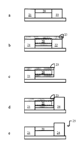
Figures 5a to 5e are schematic illustrations of successive stages in a third
method
embodying the invention. The first stage involves fabrication of a
semiconductor nanowire
fixed to end supports 21, 22 generally as described with reference to Figure
3a above. In
this example, the nanowire is formed from Si and has a diameter of
approximately 5 to 20
nm. Next, a stressor layer 23 is formed on the nanowire and end supports as
shown in
15 Figure 5b. The stressor layer 23 here is a layer of SixNy formed by CVD
to a thickness of
about 10 to 20 nm. This stressor layer induces tensile radial strain resulting
in expansion of
nanowire 20 as indicated in the figure. At this stage, the end supports 21, 22
prevent the
nanowire from taking up longitudinal strain. In the next step shown in Figure
Sc, the end
support 22 is removed by lithographic processing. The nanowire 20, thus freed
at one end,
20 is then subjected by the stressor layer to tensile longitudinal strain,
expanding
longitudinally as indicated. In the next step, a new end support 24 is formed,
this support
being attached to the free end of nanowire 20 as shown in Figure 5d. In this
example, the
new end support 24 is formed by epitaxial growth of the same material as old
support 22.
The nanowire 20, now supported at both ends, is still subject to longitudinal
and radial
strain as indicated. Next, the stressor layer 23 is removed by a process of
dry etching. In the
resulting device 25 shown in Figure 5e, the radial strain in the nanowire has
been
eliminated through removal of the stressor layer. However, the longitudinal
strain due to
the previous effect of the stressor layer is maintained by the end supports
21, 24.
With the materials and parameters described in this example, and with
appropriate
carrier type and current flow direction (electrons on (100) and (110)
surfaces), an
improvement in carrier mobility of approximately 10 to 20 percent can be
expected as a
result of the longitudinal tensile strain. The tensile longitudinal strain
could of course be
made compressive if desired for other embodiments. Also, in some embodiments
it may be
desirable to stop at the stage of Figure 5d to maintain both longitudinal and
radial strain
CA 02819469 2013-04-15
WO 2012/066444 PCT/1B2011/054864
components. In addition, in other embodiments steps 5c to 5e might be applied
to
nanowires of Figures 3b and 4c produced by the methods described earlier.
Further, the
new end support 24 may serve as an electrode contacting the nanowire and could
be made
of a different material, such as a metal formed by a metal deposition
technique.
Embodiments might also be envisaged where the nanowire is freed in step 5c by
only
partially removing the original support 22 just sufficiently to free the
nanowire to take up
the longitudinal strain. Also, instead of initially forming a nanowire fixed
at both ends as in
Figure 5a, a nanowire may be formed which is fixed at only one end. In
particular, such
nanowires can be formed which extend perpendicularly, rather than parallel, to
the
substrate. The substrate then serves as a support at one end of the nanowire,
the other end
being free. The stressor layer can then be applied to this cantilever nanowire
structure
whereby the nanowire is subjected to radial and longitudinal strain by the
stressor layer.
An alternative method of achieving only longitudinal strain in a nanowire is
indicated in Figures 6a to 6e. Materials and processing steps here are assumed
to be
generally as those of the previous method and only key differences will be
described in the
following. In step 6b of this method, a stressor layer 33 is formed to a
thickness sufficient
to fill the gap between nanowire 30 and the substrate 35. Next, both end
supports 31 and 32
are removed. This leaves the nanowire free at both ends and supported by the
stressor layer
33 whereby the nanowire is subjected to both longitudinal and radial strain as
indicated.
Next, two new supports 36, 37 are formed attached to respective ends of the
nanowire as
shown in Figure 6d. Finally, the stressor layer is removed, eliminating the
radial strain. In
the final device 38 of this embodiment, however, the longitudinal strain due
to the previous
effect of the stressor layer is maintained by the new end supports 36, 37.
Figure 7 shows an example of a nanowire FET device embodying the invention.
The device 40 of this example is formed by first producing a device as shown
in Figure 5e
or 6e by a method as described above. The end supports for the longitudinally-
strained
nanowire 41 serve as source and drain contact pads 42, 43. A surround-gate
structure is
then formed around a central channel portion of the nanowire 41 via generally
known
processing techniques. The gate structure includes a gate dielectric 44, which
may
comprise one or more layers of insulating material, formed around nanowire 41.
A metal or
polysilicon gate contact 45 is then formed around the dielectric. Gate length
is defined to
leave exposed regions of nanowire 41 between the gate stack and the source and
drain
regions respectively. Finally, an additional layer 46 is deposited to enclose
the gate
structure and exposed regions of the nanowire between the source and drain
pads. The layer
11
CA 02819469 2013-04-15
WO 2012/066444 PCT/1B2011/054864
46 in this example is formed of Si,,Ny deposited by CVD, and serves as a
further stressor
layer for the already-longitudinally-strained nanowire 41. This stressor layer
applies
additional radial stress to the regions of nanowire between the gate and the
source/drain to
further enhance performance.
It will be seen that the embodiments described above permit tensile or
compressive
radial and longitudinal strain components to be exploited separately or
together to enhance
nanowire conductivity. Through use of a stressor layer as described above, the
entire
nanowire core can contribute to conductivity and desired strain
characteristics can be
formulated to optimize nanowire performance.
It will of course be appreciated that many changes and modifications can be
made
to the exemplary embodiments described. For example, nanowires need not have
circular
cross-sections. In general, any nanowire cross section may be employed
providing the
nanowire is accessible from all sides around its circumference (as opposed to
e.g. a fin-type
structure which is joined to support along its length) to permit formation of
the stressor
layer circumferentially surrounding the nanowire. The stressor layer can of
course be
applied to a nanowire which already has other structures formed thereon, the
methods
described above being applied to produce radial and/or longitudinal strain in
the exposed
sections of the nanowire. For example, the described methods can be applied to
a nanowire
having an existing surround-gate structure formed thereon to achieve a FET
device similar
to that of Figure 7. As discussed earlier, alternative embodiments may also
convert a semi-
metal nanowire to a semiconductor nanowire under strain induced by the
stressor layer.
While simple nanowire devices and FET devices based thereon have been
described
above, methods embodying the invention can be applied in general to produce
any device
in which a nanowire is employed as a conductor. Particular examples include
thermoelectric converters, nanowire sensors, and optoelectronic devices such
as LEDs
(light emitting diodes). As mentioned earlier, the nanowires may also be
formed
perpendicularly to the substrate, giving a vertical device geometry.
Many other changes and modifications can be made to the embodiments described
without departing from the scope of the invention.
12