Note: Descriptions are shown in the official language in which they were submitted.
CA 02819618 2013-05-31
WO 2012/075129
PCT/US2011/062625
METHOD FOR FORMING AN ULTRASOUND DEVICE, AND ASSOCIATED APPARATUS
BACKGROUND OF THE DISCLOSURE
Field of the Disclosure
Aspects of the present disclosure relate to ultrasonic transducers, and, more
particularly, to a
method of forming a connection with a laterally-facing piezoelectric
micromachined ultrasonic
transducer housed in a catheter, and associated ultrasound apparatus.
Description of Related Art
Some micromachined ultrasonic transducers (MUTs) may be configured, for
example, as a
piezoelectric micromachined ultrasonic transducer (pMUT) as disclosed in U.S.
Patent No.
7,449,821 assigned to Research Triangle Institute, also the assignee of the
present disclosure, which
is also incorporated herein in its entirety by reference.
The formation of a pMUT device, such as the pMUT device defining an air-backed
cavity
as disclosed in U.S. Patent No. 7,449,821, may involve the formation of an
electrically-conductive
connection between the first electrode (i.e., the bottom electrode) of the
transducer device, wherein
the first electrode is disposed on the front side of the substrate opposite to
the air-backed cavity of
the pMUT device, and the conformal metal layer(s) applied to the air-backed
cavity for providing
subsequent connectivity, for example, to an integrated circuit ("IC") or a
flex cable.
In some instances, one or more pMUTs, for example, arranged in a transducer
array, may be
incorporated into the end of an elongate catheter or endoscope. In those
instances, for a forward-
looking arrangement, the transducer array of pMUT devices must be arranged
such that the plane of
the piezoelectric element of each pMUT device is disposed perpendicularly to
the axis of the
catheter / endoscope. This configuration may thus limit the lateral space
about the transducer array,
between the transducer array and the catheter wall, through which signal
connections may be
established with the front side of the substrate. Further, directing such
signal connections laterally
to the transducer array to the front side thereof, may undesirably and
adversely affect the diameter
of the catheter (i.e., a larger diameter catheter may undesirably be required
in order to
accommodate the signal connections passing about the transducer array).
Where the transducer array is a one-dimensional (1D) array, external signal
connections to
the pMUT devices may be accomplished by way of a flex cable spanning the
series of pMUT
devices in the transducer array so as to be in electrical engagement with
(i.e., bonded to) each
pMUT device via the confoinial metal layer thereof For instance, As shown in
Figure 1A, in one
exemplary 1D transducer array 100 (e.g., 1x64 elements), pMUT devices forming
the array
-1-
CA 02819618 2013-05-31
WO 2012/075129
PCT/US2011/062625
elements 120 may be attached directly to a flex cable 140, with the flex cable
140 including one
electrically-conductive signal lead per pMUT device, plus a ground lead. For a
forward-looking
transducer array, the flex cable 140 is bent about the opposing ends of the
transducer array such
that the flex cable 140 can be routed through the lumen of the
catheter/endoscope which, in one
instance, may comprise an ultrasound probe. However, for a forward-looking
transducer array in a
relatively small catheter/endoscope, such an arrangement may be difficult to
implement due to the
severe bend requirement for the flex cable (i.e., about 90 degrees), which may
also be compounded
by the number of conductors comprising the flex cable and the engagement of
the electrically-
conductive signal leads to the pMUT devices (also about a bend of about 90
degrees), in order for
the transducer array to be disposed within the lumen of the
catheter/endoscope.
Further, for a forward-looking two-dimensional (2D) transducer array, signal
interconnection with the individual pMUT devices may also be difficult. That
is, for an exemplary
2D transducer array (e.g. 14x14 to 40x40 elements), there may be many more
required signal
interconnections with the pMUT devices, as compared to a 1D transducer array.
As such, more
wires and/or multilayer flex cable assemblies may be required to interconnect
with all of the pMUT
devices in the transducer array. However, as the number of wires and/or flex
cable assemblies
increases, the more difficult it becomes to bend the larger amount of signal
interconnections about
the ends of the transducer device to achieve the 90 degree bend required to
integrate the transducer
array into a catheter/endoscope. In addition, the pitch or distance between
adjacent pMUT devices
may be limited due to the required number of wires/conductors. Accordingly,
such limitations may
undesirably limit the minimum size (i.e., diameter) of the catheter/endoscope
that can readily be
achieved.
Co-pending U.S. Patent Application No. 61/329,258 (Methods for Forming a
Connection
with a Micromachined Ultrasonic Transducer, and Associated Apparatuses; filed
April 29, 2010,
and assigned to Research Triangle Institute, also the assignee of the present
application), discloses
improved methods of forming an electrically-conductive connection between a
pMUT device and,
for example, an integrated circuit ("IC"), a flex cable, or a cable assembly,
wherein individual
signal leads extend parallel to the operational direction of the transducer
array or perpendicularly to
the transducer array face to engage the respective pMUT devices in the
transducer array (see
generally, e.g., FIG. 1B). Furthermore, the '258 application discloses that
additional signal
processing integrated circuits (IC's) can be integrated between the transducer
array and the
corresponding connective elements, thereby increasing the dimension of the
transducer/connective
element stack in a longitudinal direction of the disposition thereof in the
catheter, but not increasing
-2-
CA 02819618 2013-05-31
WO 2012/075129
PCT/US2011/062625
the lateral spacing around the transducer array, thus facilitating the
configuration of the catheter to
achieve a minimal diameter for a forward-looking transducer array
configuration.
In the case of side- or lateral-looking transducer arrays, the transducer
array is arranged
such that the plane of the piezoelectric element of each transducer device is
disposed in parallel to
the axis of the catheter/endoscope. In such instances, there is relatively
more lateral space about
the transducer array, between the transducer array and the catheter wall,
along the length of the
transducer array, which may be used to attach connective elements thereto.
However, the space
between the back side of the transducer array and the catheter wall may be
limited, particularly, for
example, in catheters having an inner diameter of about 3 mm or less. Further,
the previously-
noted thicker stacks placed, for example, in a transducer element as
illustrated in FIG. 1B, and
including a transducer array, signal processing IC's and connective elements,
may not necessarily
be feasible in instances of the limited catheter inner diameter. Such a
configuration may also
undesirably impart mechanical stresses to the signal lead (which must be bent
about 90 degrees to
be routed from the transducer and along the catheter) and/or the transducer
array interface due to
the thickness of the transducer / IC stack and the limited space available
across the catheter
diameter.
One particular example of a prior art side-looking ultrasound catheter
transducer is shown
in Figure 2, wherein a piezoelectric element 200 may be attached to a flex
cable 210 using
conductive epoxy 220. A top electrode 230 and matching layer 240 may then be
deposited on the
piezoelectric element 200, and the structure is then diced using a saw,
wherein the cuts extend
down to the flex cable 210 in order to form the elements of the transducer
array 250. An acoustic
backing 260 may then be applied to the back of the flex cable 210. However,
such a configuration
may be limited with respect to the number of transducer elements that can be
practically
implemented due, for instance to the resolution limit of the signal traces of
the flex cable. For
example, for a 3 mm catheter, only 16 traces with 100 um pitch (plus ground
strips on each side)
may fit laterally within the lumen of the catheter. As such, an appropriate
flex cable, such as a
Siemens AcuNav flex cable with 64 elements, may undesirably have to be folded
into 4 layers of
16 traces each (plus grounds) to connect all of the elements of a 64 element
transducer array.
Further, for 2D transducer arrays, high element counts (e.g., 196 to 1,600
elements) may require
multilayer flex cabling for attachment and interconnection of all transducer
elements, further
increasing cost and complexity of the flex cabling. Multilayer flex cable
could require up to 16
levels to connect all transducer elements due to limitations, for example,
related to the pitch of
conductor traces and interlevel vias in the flex cable (i.e., typically having
a minimum of 100 um
pitch or more, depending on the number of levels). A multiple level flex cable
may thus be
-3-
CA 02819618 2013-05-31
WO 2012/075129
PCT/US2011/062625
undesirably expensive, difficult (or impossible) to manufacture, and may not
be robust due to a
relatively high probability of short circuits in light of the increased number
of metal levels and vias.
Other disadvantages of multilayer flex cabling may include higher conductor
impedance, higher
insertion loss, greater cross coupling between element traces, and higher
shunt-to-ground
.. capacitance which may reduce penetration depth compared to coaxial cabling
(though typical
coaxial cabling cannot be made with sufficiently fine pitch to be used in such
catheter applications).
Flex cabling may also be typically limited to segments of approximately 1 foot
in length. Thus for
a catheter that is 3 feet in total length, multiple flex cable segments must
be serially connected in
order to complete the electrical connection through the entire catheter,
thereby undesirably
.. increasing complexity and cost of assembly.
Thus, there exists a need in the ultrasonic transducer art, particularly with
respect to a
piezoelectric micromachined ultrasound transducer ("pMUT"), whether having an
air-backed
cavity or not, for improved methods of forming an electrically-conductive
connection between the
pMUT device and, for example, an integrated circuit ("IC") and/or
corresponding connective
.. elements. In addition, it would be desirable to reduce the thickness of a
chip stack containing the
transducer array, IC devices and flex cabling, wiring and/or connective
elements such that the chip
stack may be accommodated within the relatively small diameter of a catheter
or endoscope in a
side looking configuration, for example, in cardiovascular devices,
intravascular ultrasound
devices, or laparoscopic surgery devices. Furthermore, it would be desirable
to provide a method
.. for forming electrical connections with a transducer array having a
relatively higher transducer
element count/density that is cost efficient (i.e., relatively low cost) and
relatively manufacturable.
Such solutions should desirably be effective for 2D transducer arrays,
particularly 2D pMUT
transducer arrays, but should also be applicable to 1D transducer arrays, in
forward-looking and/or
side looking arrangements, and should desirably allow greater scalability in
the size of the probe /
.. catheter / endoscope having such transducer arrays integrated therein.
BRIEF SUMMARY OF THE DISCLOSURE
The above and other needs are met by aspects of the present disclosure,
wherein one such
aspect relates to a method of forming an ultrasound device having an
ultrasonic transducer
.. apparatus comprising a transducer device defining a device plane, and
including a piezoelectric
material disposed between a first electrode and a second electrode. Such a
method comprises
engaging the ultrasonic transducer apparatus with a surface of an interposer
device such that the
device plane of the ultrasonic transducer apparatus is substantially parallel
to the interposer device,
wherein the interposer device is greater in at least one lateral dimension
than the ultrasonic
-4-
CA 02819618 2013-05-31
WO 2012/075129
PCT/US2011/062625
transducer apparatus so as to extend laterally outward thereof along the
device plane upon
engagement therewith, and comprises at least two conductors extending
laterally therealong, with
each conductor having opposed first and second ends. An electrically-
conductive engagement is
formed between each of the first and second electrodes and the first ends of
the respective
conductors, wherein at least one of the first and second ends of each
conductor extends outwardly
of a periphery of the ultrasonic transducer apparatus in the at least one
greater lateral dimension of
the interposer device. A connection support substrate is engaged with the
interposer device about
the second ends of the conductors and outwardly of the periphery of the
ultrasonic transducer
apparatus, wherein the connection support substrate has at least two
connective elements operably
engaged therewith, so as to form an electrically-conductive engagement between
each connective
element and the respective second ends of the conductors. The ultrasonic
transducer apparatus,
engaged with the interposer device and the connection support substrate, is
then inserted into a
lumen defined by a wall of a catheter member and about an end thereof, such
that the device plane
of the ultrasonic transducer apparatus extends parallel to the wall and such
that the at least two
connective elements extend along the lumen away from the end of the catheter
member.
Another aspect of the present disclosure provides an ultrasound device,
comprising an
ultrasonic transducer apparatus including a transducer device defining a
device plane, and having a
piezoelectric material disposed between a first electrode and a second
electrode. An interposer
device has a surface configured to engage the ultrasonic transducer apparatus
such that the device
plane of the ultrasonic transducer apparatus is substantially parallel to the
interposer device. The
interposer device is greater in at least one lateral dimension than the
ultrasonic transducer apparatus
so as to extend laterally outward thereof along the device plane, and
comprises at least two
conductors extending laterally therealong, wherein each conductor has opposed
first and second
ends. The ultrasonic transducer apparatus is engaged with the interposer
device so as to form an
electrically-conductive engagement between each of the first and second
electrodes and the first
ends of the respective conductors, with at least one of the first and second
ends of each conductor
extending outwardly of a periphery of the ultrasonic transducer apparatus in
the at least one greater
lateral dimension of the interposer device. A connection support substrate is
engaged with the
interposer device about the second ends of the conductors and outwardly of the
periphery of the
ultrasonic transducer apparatus. The connection support substrate has at least
two connective
elements operably engaged therewith, and is engaged with the interposer device
so as to form an
electrically-conductive engagement between each connective element and the
respective second
ends of the conductors. A catheter member has a wall defining a lumen, wherein
the lumen is
configured to receive the ultrasonic transducer apparatus, engaged with the
interposer device and
-5-
CA 02819618 2013-05-31
WO 2012/075129
PCT/US2011/062625
the connection support substrate, about an end thereof, such that the device
plane of the ultrasonic
transducer apparatus extends parallel to the wall and such that the at least
two connective elements
extend along the lumen away from the end of the catheter member.
Aspects of the present disclosure thus address the identified needs and
provide other
advantages as otherwise detailed herein.
BRIEF DESCRIPTION OF THE SEVERAL VIEWS OF THE DRAWING(S)
Having thus described the disclosure in general terms, reference will now be
made to the
accompanying drawings, which are not necessarily drawn to scale, and wherein:
FIGS. 1A and 1B schematically illustrate a prior art arrangements for forming
a connection
with a forward-looking transducer apparatus disposed in a lumen;
FIG. 2 schematically illustrates a prior art arrangement for forming a
connection with a
side-looking transducer apparatus disposed in a lumen;
FIGS. 3 and 4 schematically illustrate an arrangement for forming a connection
with a
side-looking one-dimensional piezoelectric micromachined ultrasonic transducer
array, according
to one aspect of the disclosure;
FIGS. 5A ¨ 5C schematically illustrate an arrangement for forming a connection
support
substrate for connection with a side-looking transducer apparatus, according
to another aspect of
the disclosure;
FIGS. 6A and 6B schematically illustrate side and top views of an arrangement
for forming
a connection with a side-looking one- or two-dimensional piezoelectric
micromachined ultrasonic
transducer array, according to another aspect of the disclosure;
FIGS. 7A and 7B schematically illustrate side and top views of an arrangement
for forming
a connection with a side-looking one- or two-dimensional piezoelectric
micromachined ultrasonic
transducer array, according to yet another aspect of the disclosure; and
FIGS. 8A and 8B schematically illustrate side and top views of a side-looking
ultrasound
apparatus, according to a further aspect of the disclosure.
DETAILED DESCRIPTION OF THE DISCLOSURE
The present disclosure now will be described more fully hereinafter with
reference to the
accompanying drawings, in which some, but not all aspects of the disclosure
are shown. Indeed,
the disclosure may be embodied in many different forms and should not be
construed as being
limited to the aspects set forth herein; rather, these aspects are provided so
that this disclosure will
satisfy applicable legal requirements. Like numbers refer to like elements
throughout.
-6-
CA 02819618 2013-05-31
WO 2012/075129
PCT/US2011/062625
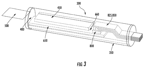
A representative ultrasound device 300, such as a catheter-based ultrasonic
transducer array,
is shown in FIG. 3. Such an exemplary aspect of the present disclosure
includes a catheter member
350 defining an axially-extending lumen 400. In such an aspect, the lumen 400
houses an
ultrasonic transducer apparatus 450, such as one or more transducer devices,
which may be
arranged in the form of a one-dimensional or two-dimensional transducer array.
The ultrasonic
transducer apparatus 450 defines a device plane 500, and each transducer
device (see, e.g., FIGS.
6A and 7A) includes a piezoelectric material 550 disposed between a first
electrode 575 and a
second electrode 600. An interposer device 650 may also be disposed within the
lumen 400. More
particularly, the interposer device 650 includes a surface 660 configured to
receive, engage and
support the ultrasonic transducer apparatus 450 such that the device plane 500
of the ultrasonic
transducer apparatus 450 is substantially parallel to the interposer device
650. The ultrasonic
transducer apparatus 450 may be secured to the surface 660, for example, by a
suitable adhesive or
epoxy. In instances where the adhesive or other securement mechanism is
involved in forming an
electrically-conductive engagement between the ultrasonic transducer apparatus
450 and the
surface 660, a conductive material such as, for example, an anisotropically-
conductive epoxy may
be used to secure the ultrasonic transducer apparatus 450 to the surface 660
of the interposer device
650. In some instances, the interposer device 650 may be comprised, for
example, of silicon or
other suitable material.
In one aspect, the interposer device 650 is greater in at least one lateral
dimension than the
ultrasonic transducer apparatus 450 (see, e.g., FIGS. 3 and 4) so as to extend
laterally outward
thereof along the device plane 500. In some instances, the interposer device
650 also includes at
least two conductors 675, 700 (See, e.g., FIGS. 4, 6B, and 7B) extending
laterally therealong,
wherein the conductors 675, 700 have opposed first ends 675A, 700A and second
ends 675B,
700B. The ultrasonic transducer apparatus 450 is engaged with the interposer
device 650 so as to
foiiii an electrically-conductive engagement between each of the first and
second electrodes 575,
600 and the first ends 675A, 700A of the respective conductors 675, 700. In
some aspects, either or
both of the opposed ends of each conductor 675, 700 may extend in conjunction
with the interposer
device 650, outwardly of a periphery of the ultrasonic transducer apparatus
450 in the one or more
greater lateral dimensions of the interposer device 650. That is, upon
engagement of the ultrasonic
transducer apparatus 450 with the interposer device 650, the interposer device
650 will extend
outwardly of the periphery of the ultrasonic transducer apparatus 450 in at
least one lateral
direction. As such, either or both of the conductors 675, 700 may have one end
thereof extending
through the interposer device 650 to the interface between the interposer
device 650 and the
-7-
CA 02819618 2013-05-31
WO 2012/075129
PCT/US2011/062625
ultrasonic transducer apparatus 450, so as to form the electrically-conductive
connection with the
ultrasonic transducer apparatus 450, wherein such an aspect is disclosed in
further detail herein.
In other aspects, either or both of the conductors 675, 700 may have one end
thereof
extending through the interposer device 650 so as to be exposed with respect
to the surface of the
interposer device 650 with which the ultrasonic transducer apparatus 450 is
engaged, but outside
the periphery of the ultrasonic transducer apparatus 450. In such instances,
the electrodes 575, 600
may be electrically-engaged with the first end(s) 675A, 700A of the conductors
675, 700 by way of
discrete conductive elements (not shown) engaged therebetween to respective
wirebond pads 250A,
250B such as, for example in a wire bonding process. Further, in some aspects,
the ultrasonic
transducer apparatus 450 (i.e., pMUT), may or may not include metalized
through-substrate
interconnects connecting the first electrode 575 to the back side of the
substrate. Accordingly, as
shown in FIG. 4, in some aspects, the signal and ground traces of the
transducer devices of the
ultrasonic transducer apparatus 450 may be routed to the peripheral edges of
the ultrasonic
transducer apparatus 450 (i.e., into electrically-conductive engagement with
wirebond pads 250A,
250B) and wirebonded to corresponding wirebond pads 250A, 250B in electrically-
conductive
engagement with the first and second conductors 675, 700 associated with the
interposer device
650. Using such a configuration of the ultrasonic transducer apparatus 450,
fewer photomask
levels, for example, are used to fabricate the transducer devices, thus
reducing fabrication costs.
However, the footprint (lateral area) of the ultrasonic transducer apparatus
450 may be required to
be larger to accommodate the wirebond pads. For instance, a 2 mm wide
ultrasonic transducer
device 450 (without metalized through-substrate interconnects) would require
about a 2.8 mm to
about a 3 mm wide interposer device 650, which would fit within the lumen of a
12 French (4 mm
0.D.) catheter. However, using metalized through-substrate interconnects,
instead of a wirebond
pad configuration, such that an electrically-conductive engagement is formed
with the conductors
675, 700 associated with the interposer device 650 by way of the conductive
layer associated with
the air-backed cavities of the transducer devices, the width of the ultrasonic
transducer device 450
could be reduced to between about 1.7 mm and about 1.8 mm, and the interposer
device 650 could
also have substantially the same width, since the additional width required
for wirebond pads is
eliminated. In such an instance, the implementation of transducer devices with
metalized through-
substrate interconnects would reduce the required catheter size to 8 French
(2.7 mm 0.D.).
As disclosed, the ultrasonic transducer apparatus 450 may be secured to the
surface 660, for
example, by a bonding material 670 such as a suitable adhesive or epoxy. In
instances where the
adhesive or other securement mechanism is involved in forming an electrically-
conductive
engagement between the ultrasonic transducer apparatus 450 and the surface
660, a conductive
-8-
CA 02819618 2013-05-31
WO 2012/075129
PCT/US2011/062625
material such as, for example, an anisotropically-conductive epoxy may be used
to secure the
ultrasonic transducer apparatus 450 to the surface 660 of the interposer
device 650. In some
instances, it may be desirable to implement an acoustically-absorbent epoxy
such as, for example, a
tungsten-filled epoxy, to secure the ultrasonic transducer apparatus 450 to
the interposer device
650, which may also provide an acoustic backing for the transducer devices. If
the ultrasonic
transducer device 450 is wirebonded to the conductors 675, 700 associated with
the interposer
device 650, a potting epoxy may be used to cover the wirebond connections.
In some aspects, the conductors 675, 700 extend laterally with respect to the
interposer
device 650 such that the second ends 675B, 700B thereof are in electrically-
conductive engagement
with an array of electrically-conductive pads 750 (see, e.g., FIG. 4), wherein
the interposer device
650 is configured to receive and engage a connection support substrate 800
such that the second
ends 675B, 700B of the conductors 675, 700, via the pads 750, engage (in an
electrically-
conductive engagement) corresponding connective elements 825, 850 (see, e.g.,
FIG. 3) engaged
with and supported by the connection support substrate 800 outwardly of the
periphery of the
ultrasonic transducer apparatus 450. The connective elements 825, 850 may
comprise, for
example, external signal leads for the ultrasonic transducer apparatus 450. As
such, in some
aspects, the ultrasonic transducer apparatus 450, engaged with the interposer
device 650 and the
connection support substrate 800, is configured to be received in an end
portion of the lumen 400
defined by a wall of the catheter member 350, such that the device plane 500
of the ultrasonic
transducer apparatus 450 extends parallel to the wall or axis of the catheter
member 350 and such
that the at least two connective elements 825, 850 extend along the lumen 400
away from the end
of the catheter member 350 (i.e., so as to form a "side-looking" ultrasound
device).
In some instances, the conductors 675, 700 associated with the interposer
device 650 may
be of different lengths due to the location and configuration of the
corresponding wirebond pad
with respect to the pads 750 for connecting with the connective elements 825,
850. As such, in
some instances, the conductors 675, 700 associated with the interposer device
650 may be
configured to have varying widths, or otherwise varying cross-sectional
dimensions, such that
differences between the electrical resistances of the conductors 675, 700 are
minimized or
substantially eliminated. That is, the conductors 675, 700 may be configured
so as to achieve and
maintain substantially constant impedance with respect to the signal leads
extending to each
transducer device of the ultrasonic transducer apparatus 450.
In some aspects, the connection support substrate 800 may be configured, for
instance, to be
compatible with a flip-chip aligner-bonder for facilitating engagement with
the interposer device
650 supporting the ultrasonic transducer apparatus 450. As such, the
interposer device 650 may
-9-
CA 02819618 2013-05-31
WO 2012/075129
PCT/US2011/062625
advantageously be configured such that the arrangement of connective elements
825, 850 with
respect to the connection support substrate 800 is not required to correspond
to the arrangement of
transducer devices in the array implemented by the ultrasonic transducer
apparatus 450. For
example, the pitch and/or gauge of the connective elements 825, 850 may be
different from the
pitch or electrode area of the transducer devices, wherein correspondence may
be achieved, if
necessary or desired, by appropriately configuring the conductors 675, 700
associated with the
interposer device 650, as will be appreciated by one skilled in the art. Such
a configuration of the
interposer device 650 may be advantageous, for example, with respect to side-
looking 1D (one-
dimensional) arrays or ultrasonic transducer apparatuses 450. For instance, as
shown in FIG. 4, a
5x16 array of wires / connective elements may be engaged with a 1x64 array of
transducer devices
in an ultrasonic transducer apparatus 450 through appropriate arrangement of
the conductors
associated with the interposer device 650. Accordingly, the implementation of
such an interposer
device may provide additional flexibility in the selection of cabling used
(i.e., in the number of
wires or connective elements per cable, as well as the wire pitch) for
connection with the ultrasonic
transducer apparatus 450, and may also allow the attachment of a
wire/connective element array
with larger number of wires (e.g., 8x16 or 128 wires) to provide additional
ground leads to be
interspersed between signal elements/wires to reduce noise and cross-talk
between conductive
elements.
FIG. 5A schematically illustrates another aspect of the present disclosure
directed to the
formation of the connection support substrate 800 and subsequent connection
thereof to the
interposer device 650. More particularly, the connection support substrate 800
(comprised, for
example, of silicon) is first etched, for example, using a DRIE process, to
define a via 802
extending therethrough with sidewalls substantially perpendicular to the
etched surface. The
connection support substrate 800 may then be thermally oxidized to provide
electrical isolation
between adjacent vias (not shown). One of the connective elements (e.g.,
element 825) is then
inserted into the via 802 so as to extend therethrough, and the connective
element 825 then bonded
to the connection support substrate 800 with a bonding material 804, such as a
non-conductive
epoxy, applied around the connective element 825 on the surface of the
connection support
substrate 800 opposite the surface of the connection support substrate 800
through which the
connective element 825 extends. For example, fine gauge (e.g., 40-50 AWG) wire
may be fed into
the via and then potted within the via with a low-viscosity epoxy in a vacuum
chamber to fill the
voids. In some instances, the connective element 825 may comprise an elongate
conductor
circumscribed by an insulator. In such instances, the insulator may be
configured to provide
electrical isolation between the conductor / connective element 825 and the
connection support
-10-
CA 02819618 2013-05-31
WO 2012/075129
PCT/US2011/062625
substrate 800. In other instances, if the connective element 825 does not
include the insulator, an
insulator material (not shown) may be first deposited on the connection
support substrate 800 so as
to extend through the via 802, so as to electrically isolate the connective
element 825 from the
connection support substrate 800.
As shown in FIG. 5B, once the connective element 825 is secured to the
connection support
substrate 800, the surface of the connection support substrate 800 through
which the connective
element 825 extends is planarized, for example, by a mechanical polishing
process or a chemical-
mechanical polishing (CMP) process to produce a substantially planar surface
having the end 806
of the connective element 825 exposed. In some instances, any gap between the
connective
element 825 and the wall defining the via 802 can be filled, for example, with
a non-conductive
epoxy to provide a void-free, planar surface of the connection support
substrate 800 for subsequent
processing. For instance, one aspect implements a microribbon cable, which
includes individually
insulated 46-48 AWG Cu wires with a Cu backplane under each ribbon to reduce
cross talk. The
microribbon cable can be fed one row at a time into the connection support
substrate 800 rather
than individual wires being guided into individual vias. The connective
element 825 and/or the
connection support substrate 800 is subsequently bonded to the interposer
device 650 and/or the
pads 750 associated therewith. In one such aspect, the conductive bonding
material 808 may
comprise, for example, a solder bump, as shown in FIG. 5C. In such instances,
the bonding may be
effectuated by reflowing the solder comprising the solder bump. In another
aspect, the conductive
bonding material 808 may comprise a metal (i.e., Au, Al, or Cu) or plated
metal stud bumps formed
using a wire bonder or by electroplating, wherein such stud bumps can be
thermo-compression
bonded to provide the electrically-conductive engagement through direct metal
bonding. An
anisotropic conductive epoxy may also be implemented as the conductive bonding
material 808.
Alignment of the connective elements 825, 850 associated with the connection
support substrate
800 with the pads 750 associated with the interposer device 650 can be
accomplished, for example,
using a flip-chip aligner-bonder. Once bonded to the pads 750, the connective
elements 825, 850
are bent about 90 degrees so as to extend substantially parallel to the device
plane 500 (but such
that the interface between the pads 750 and the connective elements 825, 850
extends
perpendicularly to the device plane 500) so as to extend along the lumen 400
of the catheter
member 350, as shown, for example, in FIGS. 6A and 7A. In some aspects, a
strain relief element
810, such as additional epoxy, as shown, for instance, in FIGS. 6A and 7A may
be applied between
the connective elements 825, 850 and the interposer device 650 for relieving
strain on the interface
between the connection support substrate 800 and the interposer device 650 (as
well as the interface
between the pads 750 and the connective elements 825, 850).
-11-
CA 02819618 2013-05-31
WO 2012/075129
PCT/US2011/062625
Other aspects of the present disclosure are provided in FIGS. 6A and 6B,
wherein the
ultrasonic transducer apparatus 450 may comprise, for example, a vertically-
integrated 1D or 2D
transducer array (i.e., pMUT transducer devices with through-substrate
interconnects). In such
instances, both the first and second electrodes 575, 600 may be accessible
with respect to one
surface of the ultrasonic transducer apparatus 450. Accordingly, the
ultrasonic transducer
apparatus 450 may be directly engaged (i.e., without wirebonding) with the
interposer device 650,
without requiring the additional area or larger lateral dimension (with
respect to both the ultrasonic
transducer apparatus 450 and the interposer device 650) for wirebond pads and
associated routing
of conductors associated therewith. In such instances, the interposer device
650 may further
comprise at least one electrically-conductive trace 1000 engaged with the
surface 660 of the
interposer device 650, wherein the trace(s) 1000 are configured to be in
electrically-conductive
engagement with the first ends 675A, 700A of the respective conductors 675,
700.
In some aspects, the ultrasonic transducer apparatus 450 may be engaged with
the interposer
device 650 such that an electrically-conductive engagement is formed between
one of the first and
second electrodes 575, 600 and the corresponding trace(s) 1000 using a bonding
material 670 such
as, for example, a conductive solder element, a conductive stud element, and a
conductive bonding
material disposed therebetween. For instance, the ultrasonic transducer
apparatus 450 can be
engaged with the surface 660 of the interposer device 650 using an anisotropic
conductive epoxy,
solder bumps, gold stud bumps or direct-plated metal bonding. The connection
support substrate
800 may be engaged with the interposer device 650 in a similar manner via a
bonding material 670
so as to form the electrically-conductive engagement between the conductors
675, 700 and the
connective elements 825, 850.
Since, in some aspects, the interposer device 650 may be comprised of silicon,
the
conductors 675, 700 and/or the trace(s) 1000 may be formed using various
semiconductor
processing techniques, as will be appreciated by one skilled in the art. For
example, conductive
material may be deposited on the interposer device 650 and patterned by
photolithography and
etching, or lift-off processing. Once the conductive material is deposited and
the conductors 675,
700 and/or the trace(s) 1000 formed, an insulator such as Si02 may be
selectively deposited over
the conductors 675, 700 and/or the trace(s) 1000 so as to prevent lateral
electrical conduction, for
instance, when an anisotropic conductive epoxy is used to engage the
ultrasonic transducer
apparatus 450 with the interposer device 650. In other instances, the
deposition of the insulator
over the conductors 675, 700 and/or the trace(s) 1000 may also prevent
electrical conduction
between the portions of the conductors 675, 700 and/or the trace(s) 1000
extending along the
-12-
CA 02819618 2013-05-31
WO 2012/075129
PCT/US2011/062625
interposer device 650 under the interface between the ultrasonic transducer
apparatus 450 and the
interposer device 650.
The pads 750, conductors 675, 700, and trace(s) 1000 may be formed as
different
metallization levels with respect to the interposer device 650, with an
insulator deposited between
levels for electrical isolation. For example, the conductors 675, 700
connecting the pads 750 to the
trace(s) 1000 may be formed as a first metallization level within the
interposer device 650, while
the pads 750 and/or the trace(s) 1000 may be formed as a second metallization
level that may
remain exposed about the surface 660. The exposed portions of the trace(s)
1000 may be
implemented for direct connection to one of the electrodes of the ultrasonic
transducer apparatus
450 or, in the case of a pMUT having an air-backed cavity, the electrodes 575,
600 on one side of
the ultrasonic transducer apparatus 450. In some instances, connection of the
second electrode 600
to the trace(s) 1000 could be accomplished by way of a conformal metallization
layer deposited in
the via comprising the air-backed cavity of the pMUT (not shown). In other
instances, the smaller
exposed pads (not shown) could be provided at the second ends 675B, 700B of
the conductors 675,
700, wherein a transducer device of the ultrasonic transducer apparatus 450
could be electrically-
engaged with the conductors 675, 700 via the small pads. In some instances,
the small exposed
pads could comprise a portion of the respective conductors, and may eliminate
multiple level
metallization requirements. However, in some aspects, as the required number
of signal leads
increases, it may be advantageous to include multiple levels of metallization
within the interposer
device 650. For example, for a 2D transducer array, 3-4 metallization levels
associated with the
interposer device 650 may be required for a transducer element count of
between about 200 and
about 400 elements, which may be advantageous, for instance, over a flex cable
approach for
connection to a 2D transducer array comprising the ultrasonic transducer
device 450, which may
require up to 16 flex cable levels due to the limitations of the available
conductor pitch, typically on
the order of 100 gm. In this regard, a 16-level multilayer flex cable may be
too expensive, difficult
to manufacture, and may not be sufficiently robust due to high probability of
shorts. Smaller
conductor pitch of between about 10 gm and about 50 gm could be fabricated,
for example, on a
silicon interposer device using silicon photolithography techniques having
improved resolution.
In some aspects, as shown in FIGS. 7A and 7B, the ultrasonic transducer device
450 (i.e., a
pMUT transducer device) disclosed herein, as necessary or desired, may be
engaged with an IC or
integrated circuit (e.g., a control IC such as an amplifier, multiplexer, or
beam former) 1100, for
example, via the interposer device 650. For instance, the IC 1100 could be
engaged with the
interposer device 650 / conductors 675, 700, between the ultrasonic transducer
device 450 and the
connection support substrate 800 using, for example, solder bumps, gold stud
bumps, metal stud
-13-
CA 02819618 2013-05-31
WO 2012/075129
PCT/US2011/062625
bumps, anisotropic conductive epoxy, or other suitable electrically-conductive
connection
provisions. In one example, the IC 1100 may be configured as an application
specific integrated
circuit (ASIC), and the interposer device 650 may thus be configured to
facilitate the integration of
the ASIC within close proximity to the ultrasonic transducer apparatus 450.
ASIC functions that
could be integrated with respect to the IC 1100 in engagement with the
interposer device 650
include, for example, amplification to enhance the small receive voltages
generated by the
transducer (pMUT) elements/devices within the array, multiplexing or switching
for toggling
transducer elements/devices between transmit mode and receive mode, timing or
beam forming for
facilitating receipt of the receive signals by the ultrasound system, and/or
multiplexing of transmit
and receive channels to reduce the number of required conductors from one
element per conductor
to multiple elements per conductor. In other instances, the IC 1100 may be
configured as charge
pump transmit circuits for generating relatively higher transmit voltages from
a relatively small
control signal sent from the ultrasound system (for example, the IC 1100 may
comprise a
multiplexer, an amplifier, a beam former, and/or a high voltage transmit
circuit). Such ASIC
functions may improve the performance of the ultrasonic transducer apparatus
450 (e.g., amplify
receive signals prior to transmission on high-capacitance system cabling)
and/or reduce the number
of connective elements required to be housed within the catheter (e.g., 4:1 or
8:1 multiplexing of
element transmit and/or receive signals by an appropriately-configured IC
1100). In such aspects,
the interposer device 650 and the conductors 675, 700 therein, may be
configured similarly to the
arrangement for receiving the ultrasonic transducer apparatus 450 (i.e., with
exposed conductive
pads in communication with the conductors 675, 700), in order to facilitate
integration of the IC
1100 (or multiple IC's) in communication with the ultrasonic transducer
apparatus 450 and the pads
750 / connective elements 825, 850 via the connection support substrate 800.
Many modifications and other aspects of the disclosures set forth herein will
come to mind
to one skilled in the art to which these disclosures pertain having the
benefit of the teachings
presented in the foregoing descriptions and the associated drawings. For
example, the exemplary
methods and aspects thereof as disclosed herein may also have related
apparatuses associated
therewith, as otherwise disclosed herein. As such, the apparatuses and methods
disclosed herein
may be suitably adapted to address such instances, within the scope of the
present disclosure.
Further, in another aspect regarding transducer (pMUT) arrays in a side-
looking catheter, as shown
in FIGS. 8A and 8B, the ultrasonic transducer apparatus 450, interposer device
650, and connection
support substrate 800 may be mounted on a catheter mount 1200 inside a
catheter transducer tip
1220, which may be configured (sized) to house the interposer device 650 and
the connection
support substrate 800 lengths (i.e., ¨2 cm). For example, the interposer
device 650 may be about
-14-
CA 02819618 2013-05-31
WO 2012/075129
PCT/US2011/062625
14.5 mm in length for a 64 element 1D transducer (pMUT) array, wherein the
array length may be
about 10.5 mm. For a 2D transducer (pMUT) array with ¨200 elements and 2 mm x
2 mm size, the
interposer device 650 could be about 6 mm in length. The catheter transducer
tip 1220 may be
sealed at the opposing distal and proximal ends thereof, while being filled
with an acoustic
coupling fluid 1240 such as, for example, glycerin, polyethylene glycol or
silicone oil. The
conductive elements (i.e., microribbon or other cabling) extends through the
proximal end of the
catheter transducer tip 1220 and along the lumen 400 defined by the catheter
member 350, and may
terminate at an electronic device, such as a circuit board (not shown), about
the proximal end of the
catheter member 350. About the distal end of the catheter member 350, a
rounded catheter cap
1260 may be engaged with or formed in the catheter transducer tip 1220 in
order to facilitate
insertion of the catheter member 350 during the medical procedure, such as an
intracardiac or
intravascular imaging process. The catheter transducer tip 1220 may also
include an acoustic lens
1280 engaged with the wall of the catheter member 350 defining the lumen 400,
opposite to the
ultrasonic transducer apparatus 450. A passive lens may be implemented to
improve image
resolution for 1D transducer arrays (i.e., 1 element only in elevation), since
such 1D arrays may not
be capable of elevation focusing, whereas a 2D transducer array may have
elevation focusing
capabilities, which may thus not require a lens. The catheter member 350 may
be comprised, for
example, of PebaxTM or any other suitable materials exhibiting, for instance,
low acoustic
impedance and low absorption, which may be particularly beneficial for the
wall of the catheter
transducer tip 1220, which requires acoustic transmission capabilities for the
ultrasonic transducer
apparatus 450. The remaining portion of the catheter member 350 may also be
comprised of
PebaxTM or other suitable material exhibiting an appropriate elastic modulus
and/or Shore hardness,
for example, to provide flexibility near the distal catheter tip for
steerability of the tip and rigidity
in the catheter shaft proximal to the tip for pushability of the catheter
member 350 through the body
of the patient. Therefore, it is to be understood that the disclosures are not
to be limited to the
specific aspects disclosed and that modifications and other aspects are
intended to be included
within the scope of the appended claims. Although specific terms are employed
herein, they are
used in a generic and descriptive sense only and not for purposes of
limitation.
-15-