Note: Descriptions are shown in the official language in which they were submitted.
CA 02819638 2013-05-31
WO 2012/075359
PCT/US2011/063000
LOW THERMAL CONDUCTIVITY MATRICES WITH EMBEDDED
NANOSTRUCTURES AND METHODS THEREOF
1. CROSS-REFERENCES TO RELATED APPLICATIONS
[0001] This application claims priority to U.S. Provisional Application No.
61/419,366,
filed December 3, 2010, commonly assigned and incorporated by reference herein
for all
purposes.
[0002] Additionally, this application is related to U.S. Patent Application
No. 13/299,179,
which is incorporated by reference herein for all purposes.
2. STATEMENT AS TO RIGHTS TO INVENTIONS MADE UNDER
FEDERALLY SPONSORED RESEARCH OR DEVELOPMENT
[0003] Work described herein has been supported, in part, by U.S. Air Force
SBIR
Contract No. FA8650-10-M-2031. The United States Government may therefore have
certain rights in the invention.
3. BACKGROUND OF THE INVENTION
[0004] The present invention is directed to nanostructures. More
particularly, the
invention provides low thermal conductivity matrices with embedded
nanostructures and
methods thereof. Merely by way of example, the invention has been applied to
arrays of
nanostructures embedded in one or more low thermal conductivity materials for
use in
thermoelectric devices. However, it would be recognized that the invention has
a much
broader range of applicability, including but not limited to use in solar
power, battery
electrodes and/or energy storage, catalysis, and/or light emitting diodes.
[0005] Thermoelectric materials are ones that, in the solid state and with
no moving parts,
can, for example, convert an appreciable amount of thermal energy into
electricity in an
applied temperature gradient (e.g., the Seebeck effect) or pump heat in an
applied electric
field (e.g., the Peltier effect). The applications for solid-state heat
engines are numerous,
including the generation of electricity from various heat sources whether
primary or waste, as
well as the cooling of spaces or objects such as microchips and sensors.
Interest in the use of
thermoelectric devices that comprise thermoelectric materials has grown in
recent years in
-1-
CA 02819638 2013-05-31
WO 2012/075359
PCT/US2011/063000
part due to advances in nano-structured materials with enhanced thermoelectric
performance
(e.g., efficiency, power density, or "thermoelectric figure of merit" ZT,
where ZT is equal to
S2o-/k and S is the Seebeck coefficient, othe electrical conductivity, and k
the thermal
conductivity of the thermoelectric material) and also due to the heightened
need both for
systems that either recover waste heat as electricity to improve energy
efficiency or cool
integrated circuits to improve their performance.
[0006] To date, thermoelectrics have had limited commercial applicability
due to the poor
cost performance of these devices compared to other technologies that
accomplish similar
means of energy generation or refrigeration. Where other technologies usually
are not as
suitable as thermoelectrics for use in lightweight and low footprint
applications,
thermoelectrics often have nonetheless been limited by their prohibitively
high costs.
Important in realizing the usefulness of thermoelectrics in commercial
applications is the
manufacturability of devices that comprise high-performance thermoelectric
materials (e.g.,
modules). These modules are preferably produced in such a way that ensures,
for example,
maximum performance at minimum cost.
[0007] The thermoelectric materials in presently available commercial
thermoelectric
modules are generally comprised of bismuth telluride or lead telluride, which
are both toxic,
difficult to manufacture with, and expensive to procure and process. With a
strong present
need for both alternative energy production and microscale cooling
capabilities, the driving
force for highly manufacturable, low cost, high performance thermoelectrics is
growing.
[0008] Thermoelectric devices are often divided into thermoelectric legs
made by
conventional thermoelectric materials such as Bi2Te3 and PbTe, contacted
electrically, and
assembled in a refrigeration (e.g., Peltier) or energy conversion (e.g.,
Seebeck) device. This
often involves bonding the thermoelectric legs to metal contacts in a
configuration that allows
a series-configured electrical connection while providing a thermally parallel
configuration,
so as to establish a temperature gradient across all the legs simultaneously.
However, many
drawbacks may exist in the production of conventional thermoelectric devices.
For example,
costs associated with processing and assembling the thermoelectric legs made
externally is
often high. The conventional processing or assembling method usually makes it
difficult to
manufacture compact thermoelectric devices needed for many thermoelectric
applications.
Conventional thermoelectric materials are usually toxic and expensive.
-2-
CA 02819638 2013-05-31
WO 2012/075359
PCT/US2011/063000
[0009] Nanostructures often refer to structures that have at least one
structural dimension
measured on the nanoscale (e.g., between 0.1 nm and 1000 nm). For example, a
nanowire is
characterized as having a cross-sectional area that has a distance across that
is measured on
the nanoscale, even though the nanowire may be considerably longer in length.
In another
example, a nanotube, or hollow nanowire, is characterized by having a wall
thickness and
total cross-sectional area that has a distance across that is measured on the
nanoscale, even
though the nanotube may be considerably longer in length. In yet another
example, a
nanohole is characterized as a void having a cross-sectional area that has a
distance across
that is measured on the nanoscale, even though the nanohole may be
considerably longer in
depth. In yet another example, a nanomesh is an array, sometimes interlinked,
including a
plurality of other nanostructures such as nanowires, nanotubes, and/or
nanoholes.
[0010] Nanostructures have shown promise for improving thermoelectric
performance.
The creation of OD, 1D, or 2D nanostructures from a thermoelectric material
may improve
the thermoelectric power generation or cooling efficiency of that material in
some instances,
and sometimes very significantly (a factor of 100 or greater) in other
instances. However,
many limitations exist in terms of alignment, scale, and mechanical strength
for the
nanostructures needed in an actual macroscopic thermoelectric device
comprising many
nanostructures. Processing such nanostructures using methods that are similar
to the
processing of silicon would have tremendous cost advantages. For example,
creating
nanostructure arrays with planar surfaces supports planar semiconductor
processes like
metallization.
[0011] Hence, it is highly desirable to form these arrays of nanostructures
from materials
with advantageous electrical, thermal, and mechanical properties for use in
thermoelectric
devices.
3. BRIEF SUMMARY OF THE INVENTION
[0012] The present invention is directed to nanostructures. More
particularly, the
invention provides low thermal conductivity matrices with embedded
nanostructures and
methods thereof. Merely by way of example, the invention has been applied to
arrays of
nanostructures embedded in one or more low thermal conductivity materials for
use in
thermoelectric devices. However, it would be recognized that the invention has
a much
-3-
CA 02819638 2013-05-31
WO 2012/075359
PCT/US2011/063000
broader range of applicability, including but not limited to use in solar
power, battery
electrodes and/or energy storage, catalysis, and/or light emitting diodes.
[0013] According to one embodiment, a matrix with at least one embedded
array of
nanowires includes nanowires and one or more fill materials located between
the nanowires.
Each of the nanowires including a first end and a second end. The nanowires
are
substantially parallel to each other and are fixed in position relative to
each other by the one
or more fill materials. Each of the one or more fill materials is associated
with a thermal
conductivity less than 50 Watts per meter per degree Kelvin. And, the matrix
is associated
with at least a sublimation temperature and a melting temperature, the
sublimation
temperature and the melting temperature each being above 350 C.
[0014] According to another embodiment, a matrix with at least one embedded
array of
nanostructures includes nanostructures, the nanostructures include first ends
and second ends
respectively. The nanostructures corresponding to voids. One or more fill
materials located
at least within the voids. Each of the nanostructures includes a semiconductor
material. The
nanostructures are substantially parallel to each other and are fixed in
position relative to each
other by the one or more fill materials. Each of the one or more fill
materials is associated
with a thermal conductivity less than 50 Watts per meter per degree Kelvin.
And, the matrix
is associated with at least a sublimation temperature and a melting
temperature, the
sublimation temperature and the melting temperature each being above 350 C.
[0015] According to yet another embodiment, a method for making a matrix
with at least
one embedded array of nanostructures includes filling voids corresponding to
nanostructures
with at least one or more fill materials, each of the one or more fill
materials being associated
with a thermal conductivity less than 50 Watts per meter per degree Kelvin,
the
nanostructures including a semiconductor material and forming a matrix
embedded with at
least the nanostructures, the matrix being associated with at least a
sublimation temperature
and a melting temperature, the sublimation temperature and the melting
temperature each
being above 350 C. The process for filling the voids includes keeping the
nanostructures
substantially parallel to each other and fixing the nanostructures in position
relative to each
other by the one or more fill materials.
[0016] Depending upon the embodiment, one or more of these benefits may be
achieved.
These benefits and various additional objects, features, and advantages of the
present
-4-
CA 02819638 2013-05-31
WO 2012/075359
PCT/US2011/063000
invention can be fully appreciated with reference to the detailed description
and
accompanying drawings that follow.
4. BRIEF DESCRIPTION OF THE DRAWINGS
[0017] Figure 1 is a simplified diagram showing an array of nanowires
embedded in a
matrix according to one embodiment of the present invention.
[0018] Figure 2 is a simplified diagram showing an array of nanoholes
embedded in a
matrix according to another embodiment of the present invention.
[0019] Figure 3 is a simplified diagram showing a method for forming an
array of
nanostructures embedded in a matrix according to one embodiment of the present
invention.
[0020] Figure 4 is a simplified diagram showing the process for forming an
array of
nanostructures as part of the method for forming an array of nanostructures
embedded in a
matrix according to one embodiment of the present invention.
[0021] Figure 5 is a simplified diagram showing an array of nanostructures
formed as
part of the method for founing an array of nanostructures embedded in a matrix
according to
one embodiment of the present invention.
[0022] Figures 6A, 6B, and 6C are scanning electron microscope images
showing various
views of the plurality of nanostructures as part of the method for forming an
array of
nano structure embedded in a matrix according to certain embodiments of the
present
invention.
[0023] Figure 7 is a simplified diagram showing formation of a first array
of
nanostructures and a second array of nanostructures as part of the method for
founing an
array of nanostructures embedded in a matrix according to one embodiment of
the present
invention.
[0024] Figure 8 is a simplified diagram showing formation of a first array
of
nanostructures and a second array of nanostructures as part of the method for
folining an
array of nanostructures embedded in a matrix according to another embodiment
of the present
invention.
[0025] Figure 9 is a simplified diagram showing a side view of the array of
nanostructures during a spin-on coating process used to fill the array of
nanostructures during
-5-
CA 02819638 2013-05-31
WO 2012/075359
PCT/US2011/063000
the fill process as part of the method of Figure 3 according to one embodiment
of the present
invention.
[0026] Figure 10 is a simplified diagram showing a side view of the array
of
nanostructures after a spin-on coating process is used to fill the array of
nanostructures as part
of the method of Figure 3 according to one embodiment of the present
invention.
[0027] Figures 11A-11F are scanning electron microscope images showing
various views
of the array of nanostructures after the spin-on coating process as part of
the method of
Figure 3 according to certain embodiments of the present invention.
[0028] Figure 12 is a simplified diagram showing a side view of the array
of
nanostructures during a deposition process used to fill the array of
nanostructures as part of
the method of Figure 3 according to one embodiment of the present invention.
5. DETAILED DESCRIPTION OF THE INVENTION
[0029] The present invention is directed to nanostructures. More
particularly, the
invention provides low thermal conductivity matrices with embedded
nanostructures and
methods thereof. Merely by way of example, the invention has been applied to
arrays of
nanostructures embedded in one or more low thermal conductivity materials for
use in
thermoelectric devices. However, it would be recognized that the invention has
a much
broader range of applicability, including but not limited to use in solar
power, battery
electrodes and/or energy storage, catalysis, and/or light emitting diodes.
[0030] In general, the usefulness of a thermoelectric material depends upon
the physical
geometry of the material. For example, the larger the surface area of the
thermoelectric
material that is presented on the hot and cold sides of a thermoelectric
device, the greater the
ability of the thermoelectric device to support heat and/or energy transfer
through an increase
in power density. In another example, a suitable minimum distance (i.e., the
length of the
thermoelectric nanostructure) between the hot and cold sides of the
thermoelectric material
help to better support a higher thermal gradient across the thermoelectric
device. This in turn
may increase the ability to support heat and/or energy transfer by increasing
power density.
[0031] One type of thermoelectric nanostructure is an array of nanowires
with suitable
thermoelectric properties. Nanowires can have advantageous thermoelectric
properties, but
to date, conventional nanowires and nanowire arrays have been limited in their
technological
-6-
CA 02819638 2013-05-31
WO 2012/075359
PCT/US2011/063000
applicability due to the relatively small sizes of arrays and the short
lengths of fabricated
nanowires. Another type of nanostructure with thermoelectric applicability is
nanoholes or
nanomeshes. Nanohole or nanomesh arrays also have limited applicability due to
the small
volumes into which these nanostructures can be created or synthesized. For
example,
conventional nanostructures with lengths shorter than 100 um have limited
applicability in
power generation and/or heat pumping, and conventional nanostructures with
lengths shorter
than 10 um have even less applicability because the ability to maintain or
establish a
temperature gradient using available heat exchange technology across these
short lengths is
greatly diminished. Furthermore, in another example, arrays smaller than the
wafer
dimensions of 4, 6, 8, and 12 inches are commercially limited.
[0032] The development of large arrays of very long nanostructures formed
using
semiconductor materials, such as silicon, can be useful in the formation of
thermoelectric
devices. For example, silicon nanostructures that have a low thermal
conductivity, and
formed within a predetermined area of a semiconductor substrate can be
utilized to form a
plurality of thermoelectric elements for making a uniwafer thermoelectric
device. In another
example, silicon nanowires formed within the predetermined area of the
semiconductor
substrate can be utilized as the n- or p-type legs or both in an assembled
thermoelectric
device.
[0033] However, there are often many difficulties in forming and utilizing
arrays of
nanostructures. For example, the nanostructures are often fragile and can be
easily bent or
broken. In another example, the nanostructures cannot be directly applied to
high
temperature surfaces. In yet another example, the nanostructures cannot be
exposed to harsh
environments. In yet another example, the nanostructures need a support
material to form
reliable planar metallic contacts required for thermoelectric applications.
Consequently,
arrays of nanostructures would benefit from being embedded in a suitable
matrix.
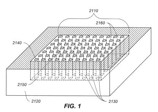
[0034] Figure 1 is a simplified diagram showing an array of nanowires
embedded in a
matrix according to one embodiment of the present invention. This diagram is
merely an
example, which should not unduly limit the scope of the claims. One of
ordinary skill in the
art would recognize many variations, alternatives, and modifications. In
Figure 1, an array of
nanowires 2110 is formed in a block of semiconductor material (e.g., a
semiconductor
substrate 2120). In one example, the semiconductor substrate 2120 is an entire
wafer. In
another example, the semiconductor substrate 2120 is a 4-inch wafer. In yet
another
-7-
CA 02819638 2013-05-31
WO 2012/075359
PCT/US2011/063000
example, the semiconductor substrate is a panel larger then a 4-inch wafer. In
another
example, the semiconductor substrate 2120 is a 6-inch wafer. In another
example, the
semiconductor substrate 2120 is an 8-inch wafer. In another example, the
semiconductor
substrate 2120 is a 12-inch wafer. In yet another example, the semiconductor
substrate 2120
is a panel larger then a 12-inch wafer. In yet another example, the
semiconductor substrate
2120 is in a shape other than that of a wafer. In yet another example, the
semiconductor
substrate 2120 includes silicon.
[0035] In some embodiments, the semiconductor substrate 2120 is
functionalized. For
example, the semiconductor substrate 2120 is doped to form an n-type
semiconductor. In
another example, the semiconductor substrate 2120 is doped to form a p-type
semiconductor.
In yet another example, the semiconductor substrate 2120 is doped using Group
III and/or
Group V elements. In yet another example, the semiconductor substrate 2120 is
functionalized to control the electrical and/or thermal properties of the
semiconductor
substrate 2120. In yet another example, the semiconductor substrate 2120
includes silicon
doped with boron. In yet another example, the semiconductor substrate 2120 is
doped to
adjust the resistivity of the semiconductor substrate 2120 to between
approximately 0.00001
O-m and 10 C2-m. In yet another example, the semiconductor substrate 2120 is
functionalized to provide the array of nanowires 2110 with a thermal
conductivity between
0.1 W/(m=K) (i.e., Watts per meter per degree Kelvin) and 500 W/(msK).
[0036] In other embodiments, the array of nanowires 2110 is formed in the
semiconductor substrate 2120. For example, the array of nanowires 2110 is
formed in
substantially all of the semiconductor substrate 2120. In another example, the
array of
nanowires 2110 includes a plurality of nanowires 2130. In yet another example,
each of the
plurality of nanowires 2130 has a first end 2140 and a second end 2150. In yet
another
example, the second ends 2150 of the plurality of nanowires 2130 collectively
form an array
area. In yet another example, the array area is 0.01 mm by 0.01 mm. In yet
another example,
the array area is 0.1 mm by 0.1 mm. In yet another example, the array area is
450 mm in
diameter. In yet another example, a distance between each of the first ends
2140 of the
plurality of nanowires 2130 and the second ends 2150 of each of the plurality
of nanowires
2130 is at least 200 p.m. In yet another example, the distance between each of
the first ends
2140 of the plurality of nanowires 2130 and the second ends 2150 of each of
the plurality of
nanowires 2130 is at least 300 pm. In yet another example, the distance
between each of the
first ends 2140 of the plurality of nanowires 2130 and the second ends 2150 of
each of the
-8-
CA 02819638 2013-05-31
WO 2012/075359
PCT/US2011/063000
plurality of nanowires 2130 is at least 400 !am. In yet another example, the
distance between
each of the first ends 2140 of the plurality of nanowires 2130 and the second
ends 2150 of
each of the plurality of nanowires 2130 is at least 500 pm. In yet another
example, the
distance between each of the first ends 2140 of the plurality of nanowires
2130 and the
second ends 2150 of each of the plurality of nanowires 2130 is at least 525
!am.
[0037] In yet another example, all the nanowires of the plurality of
nanowires 2130 are
substantially parallel to each other. In yet another example, the plurality of
nanowires 2130
is formed substantially vertically in the semiconductor substrate 2120. In yet
another
example, the plurality of nanowires 2130 are oriented substantially
perpendicular to the array
area. In yet another example, each of the plurality of nanowires 2130 has a
roughened
surface. In yet another example, each of the plurality of nanowires 2130
includes a
substantially uniform cross-sectional area with a large ratio of length to
cross-sectional area.
In yet another example, the cross-sectional area of each of the plurality of
nanowires 2130 is
substantially circular. In yet another example, the cross-sectional area of
each of the plurality
of nanowires 2130 is between 1 nm to 250 nm across.
[0038] In yet other embodiments, the plurality of nanowires 2130 have
respective
spacings 2160 between them. For example, each of the respective spacings 2160
is between
25 nm to 1000 nm across. In another example, the respective spacings 2160 are
substantially
filled with one or more fill materials. In yet another example, the one or
more fill materials
form a matrix. In yet another example, the matrix is porous. In yet another
example, the one
or more fill materials have a low thermal conductivity. In yet another
example, the thermal
conductivity is between 0.0001 W/(m=K) and 50 W/(m-K). In yet another example,
the one
or more fill materials provide added mechanical stability to the plurality of
nanowires 2130.
In yet another example, the one or more fill materials are able to withstand
temperatures in
excess of 350 C for extended periods of device operation. In yet another
example, the one
or more fill materials are able to withstand temperatures in excess of 550 C
for extended
periods of device operation. In yet another example, the one or more fill
materials are able to
withstand temperatures in excess of 650 C for extended periods of device
operation. In yet
another example, the one or more fill materials are able to withstand
temperatures in excess
of 750 C. In yet another example, the one or more fill materials are able to
withstand
temperatures in excess of 800 C . In yet another example, the one or more
fill materials have
a low coefficient of thermal expansion. In yet another example, the linear
coefficient of
thermal expansion is between 0.01 i_tm/m-K. and 301.1m/m.K. In yet another
example, the
-9-
CA 02819638 2013-05-31
WO 2012/075359
PCT/US2011/063000
one or more fill materials are able to be planarized. In yet another example,
the one or more
fill materials are able to be polished. In yet another example, the one or
more fill materials
provide a support base for additional material overlying thereon. In yet
another example, the
one or more fill materials are conductive. In yet another example, the one or
more fill
materials support the formation of good electrical contacts with the plurality
of nanowires
2130. In yet another example, the one or more fill materials support the
formation of good
thermal contacts with the plurality of nanowires 2130.
[0039] In yet other embodiments, the one or more fill materials each
include at least one
selected from a group consisting of photoresist, spin-on glass, spin-on
dopant, aerogel,
xerogel, and oxideõ and the like. For example, the photoresist includes long
UV wavelength
G-line (e.g., approximately 436 nm) photoresist. In another example, the
photoresist has
negative photoresist characteristics. In yet another example, the photoresist
exhibits good
adhesion to various substrate materials, including Si, GaAs, InP, and glass.
In yet another
example, the photoresist exhibits good adhesion to various metals, including
Au, Cu, and Al.
In yet another example, the spin on glass has a high dielectric constant. In
yet another
example, the spin-on dopant includes n-type and/or p-type dopants. In yet
another example,
the spin-on dopant is applied regionally with different dopants in different
areas of the array
of nanowires 2110. In yet another example, the spin-on dopant includes boron
and/or
phosphorous and the like. In yet another example, the spin-on glass includes
one or more
spin-on dopants. In yet another example, the aerogel is derived from silica
gel characterized
by an extremely low thermal conductivity of about 0.1 W/(m=K) and lower. In
yet another
example, the one or more fill materials include long chains of one or more
oxides. In yet
another example, the oxide includes A1203, FeO, Fe02, Fe203, TiO, Ti02, Zr02,
ZnO, Hf02,
CrO, Ta205, SiN, TiN, BN, Si02, AIN, CN, and/or the like.
[0040] According to some embodiments, the array of nanowires 2110 embedded
in the
one or more fill materials has useful characteristics. For example, the
embedded array of
nanowires 2110 is well aligned. In another example, the embedded array of
nanowires 2110
survives high temperature gradients without breaking. In yet another example,
the embedded
array of nanowires 2110 survives high temperature gradients without bending or
breaking of
the plurality of nanowires 2130. In yet another example, the enhanced
mechanical strength of
the embedded array of nanowires 2110 allows one or more surface polishing
and/or
planarization processes to be carried out on one or more surfaces of the
embedded array of
nanowires 2110. In yet another example, the enhanced mechanical strength of
the embedded
-10-
CA 02819638 2013-05-31
WO 2012/075359
PCT/US2011/063000
array of nanowires 2110 provides support for handling, machining, and/or
manufacturing
processes to be carried out on the embedded array of nanowires 2110. In yet
another
example, one or more conductive materials is placed on the embedded array of
nanowires to
foiiii one or more electric contacts with one or more pluralities of first
ends 2140 of one or
more pluralities of the nanowires 2130. In yet another example, the one or
more conductive
materials is configured to form one or more good thennal contacts with one or
more surfaces
for establishing one or more thermal paths through the one or more pluralities
of the
nanowires 2130 while limiting theimal leakage in the one or more fill
materials.
[0041] Figure 2 is a simplified diagram showing an array of nanoholes
embedded in a
matrix according to another embodiment of the present invention. This diagram
is merely an
example, which should not unduly limit the scope of the claims. One of
ordinary skill in the
art would recognize many variations, alternatives, and modifications. In
Figure 2, an array of
nanoholes 2210 is formed in a block of semiconductor material (e.g., a
semiconductor
substrate 2220). In one example, the semiconductor substrate 2220 is an entire
wafer. In
another example, the semiconductor substrate 2220 is a 4-inch wafer. In
another example,
the semiconductor substrate 2220 is a 6-inch wafer. In another example, the
semiconductor
substrate 2220 is an 8-inch wafer. In another example, the semiconductor
substrate 2220 is a
12-inch wafer. In yet another example, the semiconductor substrate 2220 is a
panel larger
then a 12-inch wafer. In yet another example, the semiconductor substrate 2220
is in a shape
other than that of a wafer. In yet another example, the semiconductor
substrate 2220 includes
silicon.
[0042] In some embodiments, the semiconductor substrate 2220 is
functionalized. For
example, the semiconductor substrate 2220 is doped to form an n-type
semiconductor. In
another example, the semiconductor substrate 2220 is doped to form a p-type
semiconductor.
In yet another example, the semiconductor substrate 2220 is doped using Group
III and/or
Group V elements. In yet another example, the semiconductor substrate 2220 is
functionalized to control the electrical and/or thermal properties of the
semiconductor
substrate 2220. In yet another example, the semiconductor substrate 2220
includes silicon
doped with boron. In yet another example, the semiconductor substrate 2220 is
doped to
adjust the resistivity of the semiconductor substrate 2220 to between
approximately 0.00001
Q-m and 10 C2-m. In yet another example, the semiconductor substrate 2220 is
functionalized to provide the array of nanoholes 2210 with a thermal
conductivity between
0.1 W/m.K. and 500 W/meK.
-11-
CA 02819638 2013-05-31
WO 2012/075359
PCT/US2011/063000
[0043] In other embodiments, the array of nanoholes 2210 is formed in the
semiconductor substrate 2220. For example, the array of nanoholes 2210 is
formed in
substantially all of the semiconductor substrate 2220. In another example, the
array of
nanoholes 2210 includes a plurality of nanoholes 2230. In yet another example,
each of the
plurality of nanoholes 2230 has a first end 2240 and a second end 2250. In yet
another
example, the second ends 2250 of the plurality of nanoholes 2230 collectively
form an array
area. In yet another example, the array area is 0.01 mm by 0.01 mm. In yet
another example,
the array area is 0.1 mm by 0.1 mm. In yet another example, the array area is
450 mm in
diameter. In yet another example, a distance between each of the first ends
2240 of the
plurality of nanoholes 2230 and the second ends 2250 of each of the plurality
of nanoholes
2230 is at least 200 p.m. In yet another example, the distance between each of
the first ends
2240 of the plurality of nanoholes 2230 and the second ends 2250 of each of
the plurality of
nanoholes 2230 is at least 3001.1m. In yet another example, the distance
between each of the
first ends 2240 of the plurality of nanoholes 2230 and the second ends 2250 of
each of the
plurality of nanoholes 2230 is at least 400 VIM. In yet another example, the
distance between
each of the first ends 2240 of the plurality of nanoholes 2230 and the second
ends 2250 of
each of the plurality of nanoholes 2230 is at least 5001.1m. In yet another
example, the
distance between each of the first ends 2240 of the plurality of nanoholes
2230 and the
second ends 2250 of each of the plurality of nanoholes 2230 is at least 525
VIM.
[0044] In yet another example, all the nanoholes of the plurality of
nanoholes 2230 are
substantially parallel to each other. In yet another example, the plurality of
nanoholes 2230 is
formed substantially vertically in the semiconductor substrate 2210. In yet
another example,
the plurality of nanoholes 2230 are oriented substantially perpendicular to
the array area. In
yet another example, each of the plurality of nanoholes 2230 has a roughened
surface. In yet
another example, each of the plurality of nanoholes 2230 are spaced between 25
nm to 1000
nm from each other.
[0045] In yet other embodiments, each of the plurality of nanoholes 2230
includes a
substantially uniform cross-sectional area with a large ratio of length to
cross-sectional area.
For example, the cross-sectional area of each of the plurality of nanoholes
2230 is
substantially circular. In another example, the cross-sectional area of each
of the plurality of
nanoholes 2230 is between 1 nm to 250 nm across. In yet another example, each
of the
plurality of nanoholes 2230 are substantially filled with one or more fill
materials. In yet
another example, the one or more fill materials form a matrix. In yet another
example, the
-12-
CA 02819638 2013-05-31
WO 2012/075359
PCT/US2011/063000
matrix is porous. In yet another example, the one or more fill materials have
a low thermal
conductivity. In yet another example, the thermal conductivity is between
0.0001 W/(m=K)
and 50 W/(m.1(). In yet another example, the one or more fill materials
provide added
mechanical stability to the plurality of nanoholes 2230. In yet another
example, the one or
more fill materials are able to withstand temperatures in excess of 650 C for
extended
periods of device operation. In yet another example, the one or more fill
materials are able to
withstand temperatures in excess of 750 C during subsequent device
fabrication. In yet
another example, the one or more fill materials have a low coefficient of
thermal expansion.
In yet another example, the linear coefficient of thermal expansion is between
0.01 m/m=K
and 30 l_tm/m=K. In yet another example, the one or more fill materials are
able to be
planarized. In yet another example, the one or more fill materials are able to
be polished. In
yet another example, the one or more fill materials provide a support base for
additional
material overlying thereon. In yet another example, the one or more fill
materials are
conductive. In yet another example, the one or more fill materials support the
formation of
good electrical contacts with the plurality of nanoholes 2230. In yet another
example, the one
or more fill materials support the formation of good thermal contacts with the
plurality of
nanoholes 2230.
[0046] In yet other embodiments, the one or more fill materials each
include at least one
selected from a group consisting of photoresist, spin-on glass, spin-on
dopant, aerogel,
xerogel, and oxide, and the like. For example, the photoresist includes long
UV wavelength
G-line (e.g., approximately 436 nm) photoresist. In another example, the
photoresist has
negative photoresist characteristics. In yet another example, the photoresist
exhibits good
adhesion to various substrate materials, including Si, GaAs, InP, and glass.
In yet another
example, the photoresist exhibits good adhesion to various metals, including
Au, Cu, and Al.
In yet another example, the spin on glass has a high dielectric constant. In
yet another
example, the spin-on dopant includes n-type and/or p-type dopants. In yet
another example,
the spin-on dopant is applied regionally with different dopants in different
areas of the array
of nanoholes 2210. In yet another example, the spin-on dopant includes boron
and/or
phosphorous and the like. In yet another example, the spin-on glass includes
one or more
spin-on dopants. In yet another example, the aerogel is derived from silica
gel characterized
by an extremely low thermal conductivity of about 0.1 W/(m-K) and lower. In
yet another
example, the one or more fill materials include long chains of one or more
oxides. In yet
-13-
CA 02819638 2013-05-31
WO 2012/075359
PCT/US2011/063000
another example, the oxide includes A1203, FeO, Fe02, Fe203, TiO, Ti02, Zr02,
ZnO, Hf02,
CrO, Ta205, SiN, TiN, BN, Si02, AIN, CN, and/or the like.
[0047] According to some embodiments, the array of nanoholes 2210 embedded
in the
one or more fill materials has useful characteristics. For example, the
embedded array of
nanoholes 2210 is well aligned. In another example, the embedded array of
nanoholes 2210
survives high temperature gradients without breaking. In yet another example,
the embedded
array of nanoholes 2210 survives high temperature gradients without bending or
breaking of
the semiconductor material surrounding the plurality of nanoholes 2230. In yet
another
example, the enhanced mechanical strength of the embedded array of nanoholes
2210 allows
one or more surface polishing and/or planarization processes to be carried on
one or more
surfaces of the embedded array of nanoholes 2210. In yet another example, the
enhanced
mechanical strength of the embedded array of nanoholes 2210 provides support
for handling,
machining, and/or manufacturing processes to be carried out on the embedded
array of
nanoholes 2210. In yet another example, one or more conductive materials is
placed on the
embedded array of nanowires to form one or more electric contacts with one or
more
pluralities of first ends 2140 of one or more pluralities of the nanoholes
2230. In yet another
example, the one or more conductive materials is configured to form one or
more good
thermal contacts with one or more surfaces for establishing one or more
thermal paths
through the one or more pluralities of the nanoholes 2230 while limiting
thermal leakage in
the one or more fill materials.
[0048] Figure 3 is a simplified diagram showing a method for forming an
array of
nanostructures embedded in a matrix according to one embodiment of the present
invention.
This diagram is merely an example, which should not unduly limit the scope of
the claims.
One of ordinary skill in the art would recognize many variations,
alternatives, and
modifications. The method 2300 includes a process 2310 for forming an array of
nanostructures, a process 2320 for pretreating the array of nanostructures, a
process 2330 for
preparing one or more fill materials, a process 2340 for filling the array of
nanostructures, a
process 2350 for curing the one or more fill materials, and a process 2360 for
planarizing the
filled array of nanostructures. For example, the method 2300 is used to form
the plurality of
nanowires 2130 embedded in a matrix as shown in Figure 1. In another example,
the method
2300 is used to form the plurality of nanoholes 2230 embedded in a matrix as
shown in
Figure 2. In yet another example, the processes 2320, 2350, and/or 2360 are
skipped.
-14-
CA 02819638 2013-05-31
WO 2012/075359
PCT/US2011/063000
[0049] Figure 4 is a simplified diagram showing the process 2310 for
forming an array of
nanostructures as part of the method 2300 for forming an array of
nanostructures embedded
in a matrix according to one embodiment of the present invention. This diagram
is merely an
example, which should not unduly limit the scope of the claims. One of
ordinary skill in the
art would recognize many variations, alternatives, and modifications. The
process 2310
includes a process 310 for providing the semiconductor substrate, a process
320 for
functionalizing the semiconductor substrate, a process 330 for washing the
semiconductor
substrate, a process 340 for masking portions of the semiconductor substrate,
a process 350
for applying a metalized film to the semiconductor substrate, a process 360
for etching the
semiconductor substrate, a process 370 for cleaning the etched semiconductor
substrate, and a
process 380 for drying the etched semiconductor substrate.
[0050] Figure 5 is a simplified diagram showing an array of nanostructures
foimed as
part of the method 2300 for foiming an array of nanostructures embedded in a
matrix
according to one embodiment of the present invention. This diagram is merely
an example,
which should not unduly limit the scope of the claims. One of ordinary skill
in the art would
recognize many variations, alternatives, and modifications. In Figure 5, an
array of
nanostructures 2510 is foimed in a block of semiconductor material (e.g., a
semiconductor
substrate 2520). In one example, the semiconductor substrate 2520 is an entire
wafer. In
another example, the semiconductor substrate 2520 is a 4-inch wafer. In yet
another
example, the semiconductor substrate is a panel larger then a 4-inch wafer. In
yet another
example, the semiconductor substrate 2520 includes silicon. In yet another
example, the
semiconductor substrate 2520 is the semiconductor substrate 2120 and/or the
semiconductor
substrate 2220.
[0051] In some embodiments, the semiconductor substrate 2520 is
functionalized. For
example, the semiconductor substrate 2520 is doped to form an n-type
semiconductor. In
another example, the semiconductor substrate 2520 is doped to form a p-type
semiconductor.
In yet another example, the semiconductor substrate 2520 is doped using Group
III and/or
Group V elements. In yet another example, the semiconductor substrate 2520 is
functionalized to control the electrical and/or thermal properties of the
semiconductor
substrate 2520. In yet another example, the semiconductor substrate 2520
includes silicon
doped with boron. In yet another example, the semiconductor substrate 2520 is
doped to
adjust the resistivity of the semiconductor substrate 2520 to between
approximately 0.00001
f1-m and 10 C2-m. In yet another example, the semiconductor substrate 2520 is
-15-
CA 02819638 2013-05-31
WO 2012/075359
PCT/US2011/063000
functionalized to provide the array of nanostructures 2510 with a thermal
conductivity
between 0.1 W/m-K and 500 W/m-K.
[0052] In other embodiments, the array of nanostructures 2510 is formed in
the
semiconductor substrate 2520. For example, the array of nanostructures 2510 is
formed in
substantially all of the semiconductor substrate 2520. In another example, the
array of
nanostructures 2510 includes a plurality of nanostructures 2530. In yet
another example,
each of the plurality of nanostructures 2530 has a first end 2540 and a second
end 2550. In
yet another example, the second ends 2550 of the plurality of nanostructures
2530
collectively form an array area. In yet another example, the array area is
0.01 mm by 0.01
mm. In yet another example, the array area is 0.1 mm by 0.1 mm. In yet another
example,
the array area is 450 mm in diameter. In yet another example, a distance
between each of the
first ends 2540 of the plurality of nanostructures 2530 and the second ends
2550 of each of
the plurality of nanostructures 2530 is at least 200 pm. In yet another
example, the distance
between each of the first ends 2540 of the plurality of nanostructures 2530
and the second
ends 2550 of each of the plurality of nanostructures 2530 is at least
30011111. In yet another
example, the distance between each of the first ends 2540 of the plurality of
nanostructures
2530 and the second ends 2550 of each of the plurality of nanostructures 2530
is at least 400
!AM. In yet another example, the distance between each of the first ends 2540
of the plurality
of nanostructures 2530 and the second ends 2550 of each of the plurality of
nanostructures
2530 is at least 500 p.m. In yet another example, the distance between each of
the first ends
2540 of the plurality of nanostructures 2530 and the second ends 2550 of each
of the plurality
of nanostructures 2530 is at least 525 gm.
[0053] In yet another example, all the nanostructures of the plurality of
nanostructures
2530 are substantially parallel to each other. In yet another example, the
plurality of
nanostructures 2530 is formed substantially vertically in the semiconductor
substrate 2510.
In yet another example, the plurality of nanostructures 2530 are oriented
substantially
perpendicular to the array area. In yet another example, each of the plurality
of
nanostructures 2530 has a roughened surface. In yet another example, each of
the plurality of
nanostructures 2530 are spaced between 25 nm to 1000 nm from each other. In
yet another
example, each of the plurality of nanostructures 2530 includes a substantially
uniform cross-
sectional area with a large ratio of length to cross-sectional area. In yet
another example, the
cross-sectional area of each of the plurality of nanostructures 2530 is
substantially circular.
-16-
CA 02819638 2013-05-31
WO 2012/075359
PCT/US2011/063000
In another example, the cross-sectional area of each of the plurality of
nanostructures 2530 is
between 1 nm to 1000 nm across.
[0054] According to some embodiments, the array of nanostructures 2510 is
the array of
nanowires 2110 as shown in Figure 1. For example, the plurality of
nanostructures 2530 is
the plurality of nanowires 2130. According to some embodiments, the array of
nanostructures 2510 is the array of nanoholes 2210 as shown in Figure 2. For
example, the
plurality of nanostructures 2530 is the plurality of nanoholes 2230.
[0055] As discussed above and further emphasized here, Figure 5 is merely
an example,
which should not unduly limit the scope of the claims. One of ordinary skill
in the art would
recognize many variations, alternatives, and modifications. In some
embodiments,
nanostructures other than nanowires or nanoholes are formed. For example,
nanotubes and/or
nanomeshes are formed in the semiconductor substrate 2520. In certain
embodiments, more
than one plurality of nanostructures is formed in a semiconductor substrate.
[0056] Figures 6A, 6B, and 6C are scanning electron microscope images
showing various
views of the plurality of nanostructures 2530 as part of the method 2300 for
forming an array
of nanostructure embedded in a matrix according to certain embodiments of the
present
invention. These images are merely examples, which should not unduly limit the
scope of
the claims. One of ordinary skill in the art would recognize many variations,
alternatives, and
modifications. Figures 6A and 6B show a plurality of nanowires with a large
ratio of length
to cross-sectional area and that are substantially parallel with each other.
Figure 6C shows
the top view of a plurality of nanostructures 2610 with a plurality of voids
2620 between the
plurality of nanostructures 2610. For example, the plurality of nanostructures
2610 is the
plurality of nanowires 2130 of Figure 1. In another example, the plurality of
voids 2620 are
the respective spacings 2160 of Figure 1. In yet another example, the
plurality of voids 2620
is the plurality of nanoholes 2230 of Figure 2.
[0057] Figure 7 is a simplified diagram showing formation of a first array
of
nanostructures and a second array of nanostructures as part of the method 2300
for forming
an array of nanostructures embedded in a matrix according to one embodiment of
the present
invention. This diagram is merely an example, which should not unduly limit
the scope of
the claims. One of ordinary skill in the art would recognize many variations,
alternatives, and
modifications. For example, as shown in Figure 7, the semiconductor substrate
2710
includes the first array of nanostructures 2720 and the second array of
nanostructures 2730.
-17-
CA 02819638 2013-05-31
WO 2012/075359
PCT/US2011/063000
In another example, the semiconductor substrate 2710 is the semiconductor
substrate 2520.
In yet another example, the first array of nanostructures 2720 and the second
array of
nanostructures 2730 are the array of nanostructures 2510.
[0058] Figure 8 is a simplified diagram showing formation of a first array
of
nanostructures and a second array of nanostructures as part of the method 2300
for forming
an array of nanostructures embedded in a matrix according to another
embodiment of the
present invention. This diagram is merely an example, which should not unduly
limit the
scope of the claims. One of ordinary skill in the art would recognize many
variations,
alternatives, and modifications. For example, as shown in Figure 8, the
semiconductor
substrate 2810 includes the first array of nanostructures 2820 and the second
array of
nanostructures 2830. In another example, the semiconductor substrate 2810 is
the
semiconductor substrate 2520. In yet another example, the first array of
nanostructures 2820
and the second array of nanostructures 2830 are the array of nanostructures
2510.
[0059] Referring back to Figure 3, at the optional process 2320, the array
of
nanostructures is pretreated. For example, the hydrophobicity of each of the
surfaces of each
of the plurality of nanostructures in the array of nanostructures is altered.
In another
example, the surface energy of each of the surfaces of each of the plurality
of nanostructures
is modified. In yet another example, each of the surfaces of each of the
plurality of
nanostructures is made more hydrophobic. In yet another example, each of the
surfaces of
each of the plurality of nanostructures is made more hydrophilic. In yet
another example,
each of the surfaces of each of the plurality of nanostructures are pretreated
by thermal
diffusion. In yet another example, each of the surfaces of each of the
plurality of
nanostructures are pretreated by doping. In yet another example, each of the
surfaces of each
of the plurality of nanostructures are pretreated using ultraviolet (UV)
light. In yet another
example, each of the surfaces of each of the plurality of nanostructures are
pretreated using
ozone.
[0060] According to one embodiment, at the process 2330, one or more fill
materials are
prepared. For example, the one or more fill materials have a low thermal
conductivity. In yet
another example, the thermal conductivity is between 0.0001 W/(m=K) and 50
W/(m=K). In
yet another example, the one or more fill materials provide added mechanical
stability to the
plurality of nanostructures 2530. In yet another example, the one or more fill
materials are
able to withstand temperatures in excess of 650 C for extended periods of
device operation.
-18-
CA 02819638 2013-05-31
WO 2012/075359
PCT/US2011/063000
In yet another example, the one or more fill materials are able to withstand
temperatures in
excess of 750 C during subsequent device fabrication. In yet another example,
the linear
coefficient of thermal expansion is between 0.01 pm/m-1( and 30 j.tm/m.K. In
yet another
example, the one or more fill materials are able to be planarized. In yet
another example, the
one or more fill materials are able to be polished. In yet another example,
the one or more fill
materials provide a support base for additional material overlying thereon. In
yet another
example, the one or more fill materials are conductive. In yet another
example, the one or
more fill materials support the formation of good electrical contacts with the
plurality of
nanostructures 2530. In yet another example, the one or more fill materials
support the
formation of good thermal contacts with the plurality of nanostructures 2530.
[0061] In another embodiment, the one or more fill materials each include
at least one
selected from a group consisting of photoresist, spin-on glass, spin-on
dopant, aerogel,
xerogel, and oxide, and the like. For example, the one or more photoresists
include long UV
wavelength G-line photoresist. For example, the photoresist includes long UV
wavelength
G-line (e.g., approximately 436 nm) photoresist. In another example, the
photoresist has
negative photoresist characteristics. In yet another example, the photoresist
exhibits good
adhesion to various substrate materials, including Si, GaAs, InP, and glass.
In yet another
example, the photoresist exhibits good adhesion to various metals, including
Au, Cu, and Al.
In yet another example, the spin on glass has a high dielectric constant. In
yet another
example, the spin-on dopant includes n-type and/or p-type dopants. In yet
another example,
the spin-on dopant is applied regionally with different dopants in different
areas of the array
of nanostructures. In yet another example, the spin-on dopant includes boron
and/or
phosphorous and the like. In yet another example, the spin-on glass includes
one or more
spin-on dopants. In yet another example, the aerogel is derived from silica
gel characterized
by an extremely low thermal conductivity of about 0.1 W/(m-K) and lower. In
yet another
example, the one or more fill materials include long chains of one or more
oxides. In yet
another example, the oxide includes A1203, FeO, Fe02, Fe203, TiO, Ti02, Zr02,
ZnO, Hf02,
CrO, Ta205, SiN, TiN, BN, 5i02, A1N, CN, and/or the like.
[0062] In yet another embodiment, the one or more fill materials are
prepared for use.
For example, the one or more fill materials are placed into solution using one
or more
solvents. In another example, the one or more solvents include one or more
selected from a
group consisting of alcohol, acetone, and/or a non-polar solvent and the like.
In yet another
example, the one or more solvents include alcohol, acetone, and/or the like
when the surfaces
-19-
CA 02819638 2013-05-31
WO 2012/075359
PCT/US2011/063000
of each of the plurality of nanostructures are hydrophilic. In yet another
example, the one or
more solvents include one or more non-polar solvents when the surfaces of each
of the
plurality of nanostructures are hydrophobic. In yet another example, the one
or more fill
materials are prepared by heating them until they are in liquid form. In yet
another example,
the one or more fill materials are doped using one or more dopants.
[0063] At the process 2340, the array of nanostructures is filled using the
one or more fill
materials. For example, the one or more fill materials are used to form a
matrix. In another
example, the matrix embeds the plurality of nanostructures. In yet another
example, the array
of nanostructures corresponds to a plurality of voids. In yet another example,
the plurality of
voids is filled by the one or more fill materials. In yet another example, the
process 2340
uses different filling processes. In yet another example, the choice of fill
process depends on
the one or more fill materials to be used. In yet another example, the choice
of fill process
depends on the desired composition and profile of the matrix to be created.
[0064] Figure 9 is a simplified diagram showing a side view of the array of
nanostructures 2510 during a spin-on coating process used to fill the array of
nanostructures
2510 during the fill process 2340 as part of the method of Figure 3 according
to one
embodiment of the present invention. This diagram is merely an example, which
should not
unduly limit the scope of the claims. One of ordinary skill in the art would
recognize many
variations, alternatives, and modifications. As shown in Figure 9, the spin-on
coating process
is used with one or more fill materials in liquid form. In another example,
the spin-on
coating technique uses photoresists, one or more spin-on glasses, one or more
spin-on
dopants, aerogel, and/or xerogel and the like as the one or more fill
materials. In yet another
example, an excess amount of the one or more fill materials 2910 is placed
onto the array of
nanostructures 2510. In yet another example, the array of nanostructures 2510
and the
semiconductor substrate 2520 are rotated at high speed. In yet another
example, the one or
more fill materials 2910 spread out by centrifugal force to fill the array of
nanostructures
2510. In yet another example, excess amounts of the one or more fill materials
spins out of
the array of nanostructures 2510 and off the edges of the semiconductor
substrate 2520. In
yet another example, the amount of the one or more fill materials 2920 is
determined and/or
systematically optimized to ensure that all regions of the array of
nanostructures 2510 is
slightly over-filled. In yet another example, the spin-on coating process is
aided by capillary
force.
-20-
CA 02819638 2013-05-31
WO 2012/075359
PCT/US2011/063000
[0065] Figure 10 is a simplified diagram showing a side view of the array
of
nanostructures 2510 after a spin-on coating process is used to fill the array
of nanostructures
2510 as part of the method of Figure 3 according to one embodiment of the
present invention.
This diagram is merely an example, which should not unduly limit the scope of
the claims.
One of ordinary skill in the art would recognize many variations,
alternatives, and
modifications. As shown in Figure 10, the one or more fill materials 2920 is
distributed
throughout the array of nanostructures 2510. For example, a desired coverage
of the one or
more fill materials 2920 overlays the array of nanostructures 2510. In another
example, a
greater amount of the one or more fill materials 2920 is positioned at the
edges 2930 of the
array of nanostructures 2510 than is positioned at the center 2940 of the
array of
nanostructures 2510. In yet another example, the non-unifoimity of the one or
more fill
materials 2920 between the edges 2930 and the center 2940 is substantially
less than 10%.
[0066] Figures 11A-11F are scanning electron microscope images showing
various views
of the array of nanostructures 2510 after the spin-on coating process as part
of the method of
Figure 3 according to certain embodiments of the present invention. These
images are
merely examples, which should not unduly limit the scope of the claims. One of
ordinary
skill in the art would recognize many variations, alternatives, and
modifications. As shown
in Figures 11A-11F, the one or more fill materials 2920 cover the array of
nanostructures
2510 in varying amounts based on the distance from the center 2940 of the
array of
nanostructures 2510. For example, as shown in Figures 11A and 11B, regions of
the array of
nanostructures 2510 with a distance of approximately 75 mm and 65 mm,
respectively, from
the center 2940 have a relative excessive coverage of the one or more fill
materials. In
another example, the first ends 2540 of the plurality of nanostructures 2530
at these distances
from the center 2940 are hardly visible. In yet further examples, as shown in
Figures 11C-
11F, as the images move closer to the center 2940 of the array of
nanostructures 2510, more
of the first ends 2540 of the plurality of nanostructures 2530 become visible.
[0067] In another embodiment, the process 2340, to fill the array of
nanostructures 2510
using the one or more fill materials includes a dipping process. For example,
in the dipping
process, the semiconductor substrate 2520 and the array of nanostructures 2510
is immersed
in a bath of the one or more fill materials. In another example, the dipping
process is aided
by capillary force. In yet another embodiment, a sol-gel process is used to
form long chains
of the one or more oxides as the one or more fill materials.
-21-
CA 02819638 2013-05-31
WO 2012/075359 PCT/US2011/063000
[0068] In yet another embodiment, the process 2340, to fill the array of
nanostructures
2510 using the one or more fill materials uses a deposition process. For
example, the array of
nanostructures is filled using chemical vapor deposition (CVD). In another
example, the
array of nanostructures is filled using atomic layer deposition (ALD). In yet
another
example, atomic layer deposition is used with TMOS (tetra-methyl-ortho-
silicate), an
oxidant, and/or a catalyst. In yet another example, TEOS (tetra-etho-ortho-
silicate) is
substituted for TMOS. In yet another example, silane (SiH4) is substituted for
TMOS. In yet
another example, the oxidant includes water vapor and/or ozone. In yet another
example, the
catalyst includes an amine. In yet another example, the deposition processes
are used to
create a heterogeneous fill.
[0069] Figure 12 is a simplified diagram showing a side view of the array
of
nanostructures 2510 during a deposition process used to fill the array of
nanostructures 2510
as part of the method of Figure 3 according to one embodiment of the present
invention. This
diagram is merely an example, which should not unduly limit the scope of the
claims. One of
ordinary skill in the art would recognize many variations, alternatives, and
modifications. As
shown in Figure 12, one or more fill materials is distributed throughout the
array of
nanostructures 2510 in a layered fashion. For example, at least a first fill
material is
deposited in a first fill layer 2952 on the one or more surfaces of the
plurality of
nanostructures 2950. In another example, at least a second fill material is
deposited in a
second fill layer 2954 on the first fill layer 2952. In yet another example,
at least a third fill
material is deposited in a third fill layer 2956 on the second fill layer
2954. In yet another
=
example, the first fill layer 2952, the second fill layer 2954, and/or the
third fill layer 2956
form a conformal coating on the material in the layer below it. In yet another
example, the
first fill layer 2952 provides one or more surfaces with a hydrophobicity that
is different from
the underlying surfaces of the plurality nanostructures 2950. In yet another
example, the
first fill layer 2952 provides thermal protection to the underlying the
plurality of
nanostructures 2950. In yet another example, the first fill material is SiN,
TiN, BN, AIN,
and/or CN, and the like. In yet another example, the second fill material and
the third fill
material are two dissimilar oxides. In yet another example, the second fill
material is Si02
and/or Zr02. In yet another example, the third fill material is Zr02 and/or
SiO2.
[0070] As discussed above and further emphasized here, Figure 12 is merely
an example,
which should not unduly limit the scope of the claims. One of ordinary skill
in the art would
recognize many variations, alternatives, and modifications. For example,
nanostructures
-22-
CA 02819638 2013-05-31
WO 2012/075359
PCT/US2011/063000
other than nanowires or nanoholes are formed. In another example, more than
three layers of
the one or more fill materials are used to fill the array of nanostructures.
In yet another
example, the at least second fill material and the at least third fill
material are deposited in
alternating layers until the array of nanostructures is substantially filled.
In yet another
example, different combinations of the one or more fill materials are used in
different regions
of the array of nanostructures. In yet another example, different combinations
of the one or
more fill materials having at least two distinct phases are used to fill the
array of
nanostructures.
[0071] Referring back to Figure 3, at the optional process 2350 the one or
more fill
materials are cured. For example, the curing process includes transforming the
one or more
fill materials to solid form. In another example, the curing process 2350
includes thermally
treating the one or more fill materials. In yet another example, the curing
process 2350 is
performed at about room temperature. In yet another example, the curing
process 2350 is
performed at an elevated temperature range up to a few hundred degrees
Centigrade. In yet
another example, the curing process 2350 is performed at about 500 C. In yet
another
example, the curing process 2350 is performed using a predetermined
temperature profile. In
yet another example, the curing process 2350 includes ramping up the
temperature from
about room temperature to between 50 C and 250 C over at a time period of up
to about 2
hours. In yet another example, the curing process 2350 includes heat treating
at an elevated
temperature between 300 C and 500 C for a period of up to one hour. In yet
another
example, the curing process 2350 includes a cooling off period of up to 30
minutes or longer.
In yet another example, the curing process 2350 cleans and/or drives
impurities from the one
or more fill materials. In yet another example, the curing process 2350 is
performed in a
furnace with a predetermined gaseous environment. In yet another example, the
curing
process 2350 is performed in a partial vacuum. In yet another example, the
curing process
2350 is performed in a vacuum.
[0072] At the optional process 2360, the embedded array of nanostructures
is planarized.
For example, the planarization process 2360 includes polishing. In another
example, the
planarization process 2360 prepares the embedded array of nanostructures for
further
handling, machining, and/or manufacturing processes. In yet another example,
the
planarization process 2360 provides one or more surfaces on the embedded array
of
nanostructures that are configured to receive one or more conductive
materials.
-23-
CA 02819638 2013-05-31
WO 2012/075359
PCT/US2011/063000
[0073] As discussed above and further emphasized here, Figures 3-12 are
merely
examples, which should not unduly limit the scope of the claims. One of
ordinary skill in the
art would recognize many variations, alternatives, and modifications. In some
embodiments,
nanostructures other than nanowires and nanoholes are formed and filled. For
example,
nanotubes, and/or nanomeshes are formed in the semiconductor substrate and
then filled. In
another example, the one or more fill materials form a porous matrix. In yet
another
example, the one or more fill materials form a matrix without cracks or voids.
In yet another
example, the one or more fill materials include one or more first fill
materials and one or
more second fill materials. In yet another example, the one or more first fill
materials are
used to fill a first portion of the array of nanostructures. In yet another
example, the one or
more second fill materials are used to fill a second portion of the array of
nanostructures.
[0074] In some embodiments, a plurality of fill processes is used for the
process 2340 for
filling the array of nanostructures. For example, a deposition process is used
to apply a
conformal coating to the one or more surfaces of the one or more
nanostructures. In another
example, the conformal coating is used to alter the hydrophobicity of the one
or more
surfaces instead of using the process 2320 for pretreating the array of
nanostructures.
[0075] According to one embodiment, a matrix with at least one embedded
array of
nanowires includes nanowires and one or more fill materials located between
the nanowires.
Each of the nanowires including a first end and a second end. The nanowires
are
substantially parallel to each other and are fixed in position relative to
each other by the one
or more fill materials. Each of the one or more fill materials is associated
with a thermal
conductivity less than 50 Watts per meter per degree Kelvin. And, the matrix
is associated
with at least a sublimation temperature and a melting temperature, the
sublimation
temperature and the melting temperature each being above 350 C. For example,
the matrix
is implemented according to at least Figure 1.
[0076] In another example, the matrix is a part of a thermoelectric device.
In yet another
example, the matrix further includes a plurality of nanostructures, the
plurality of
nanostructures includes the one or more fill materials. In yet another
example, a distance
between the first end and the second end is at least 300 um. In yet another
example, the
distance is at least 400 um. In yet another example, the distance is at least
500 um. In yet
another example, the distance is at least 525 um. In yet another example, the
nanowires
correspond to an area, the area being approximately 0.0001 mm2 in size. In yet
another
-24-
CA 02819638 2013-05-31
WO 2012/075359
PCT/US2011/063000
example, the nanowires correspond to an area, the area being smaller than 0.01
mm2 in size.
In yet another example, the nanowires correspond to an area, the area being at
least 100 mm2
in size. In yet another example, the area is at least 1000 mm2 in size. In yet
another
example, the area is at least 2500 mm2 in size. In yet another example, the
area is at least
5000 mm2 in size.
[0077] In yet another example, the melting temperature and the sublimation
temperature
are each above 450 C. In yet another example, the melting temperature and the
sublimation
temperature are each above 550 C. In yet another example, the melting
temperature and the
sublimation temperature are each above 650 C. In yet another example, the
melting
temperature and the sublimation temperature are each above 750 C. In yet
another example,
the melting temperature and the sublimation temperature are each above 800 C.
In yet
another example, the thermal conductivity is less than 5 Watts per meter per
degree Kelvin.
In yet another example, the thermal conductivity is less than 1 Watts per
meter per degree
Kelvin. In yet another example, the thermal conductivity is less than 0.1
Watts per meter per
degree Kelvin. In yet another example, the thermal conductivity is less than
0.01 Watts per
meter per degree Kelvin. In yet another example, the thermal conductivity is
less than 0.001
Watts per meter per degree Kelvin. In yet another example, the thermal
conductivity is less
than 0.0001 Watts per meter per degree Kelvin.
[0078] In yet another example, the one or more fill materials each include
at least one
selected from a group consisting of photoresist, spin-on glass, spin-on
dopant, aerogel,
xerogel, and oxide. In yet another example, the photoresist is G-line
photoresist. In yet
another example, the oxide is selected from a group consisting of A1203, FeO,
Fe02, Fe203,
TiO, Ti02, Zr02, ZnO, Hf02, CrO, Ta205, SiN, TiN, BN, Si02, MN, and CN. In yet
another
example, the one or more fill materials include one or more long chains of one
or more
oxides. In yet another example, the matrix is porous. In yet another example,
surfaces of the
nanowires are hydrophilic. In yet another example, surfaces of the nanowires
are
hydrophobic. In yet another example, at least one surface of the matrix is
planarized.
[0079] In yet another example, the one or more fill materials are in
different layers
respectively. In yet another example, the different layers include a first
layer, a second layer,
and a third layer. The first layer includes one or more materials selected
from a group
consisting of SiN, TiN, BN, AIN, and CN. The second layer includes a first
oxide. And, the
third layer includes a second oxide. In yet another example, the first oxide
is Si02 and the
-25-
CA 02819638 2013-05-31
WO 2012/075359
PCT/US2011/063000
second oxide is Zr02. In yet another example, the first layer is on the
nanowires, the second
layer is on the first layer, and the third layer is on the second layer. In
yet another example,
the different layers further include a fourth layer and a fifth layer. The
fourth layer includes
the first oxide and the fifth layer includes the second oxide. In yet another
example, the
matrix includes a first region and a second region. The one or more fill
materials include one
or more first materials located in the first region and one or more second
materials located in
the second region. In yet another example, the nanowires include a
semiconductor. In yet
another example, the semiconductor is silicon.
[0080] According to another embodiment, a matrix with at least one embedded
array of
nanostructures includes nanostructures, the nanostructures include first ends
and second ends
respectively. The nanostructures corresponding to voids. One or more fill
materials located
at least within the voids. Each of the nanostructures includes a semiconductor
material. The
nanostructures are substantially parallel to each other and are fixed in
position relative to each
other by the one or more fill materials. Each of the one or more fill
materials is associated
with a thermal conductivity less than 50 Watts per meter per degree Kelvin.
And, the matrix
is associated with at least a sublimation temperature and a melting
temperature, the
sublimation temperature and the melting temperature each being above 350 C.
For example,
the matrix is implemented according to at least Figure 2.
[0081] In another example, the nanostructures correspond to nanoholes and
the nanoholes
are the voids. In yet another example, the nanostructures correspond to
nanowires and spaces
surrounding the nanowires are the voids.
[0082] According to yet another embodiment, a method for making a matrix
with at least
one embedded array of nanostructures includes filling voids corresponding to
nanostructures
with at least one or more fill materials, each of the one or more fill
materials being associated
with a thermal conductivity less than 50 Watts per meter per degree Kelvin,
the
nanostructures including a semiconductor material and forming a matrix
embedded with at
least the nanostructures, the matrix being associated with at least a
sublimation temperature
and a melting temperature, the sublimation temperature and the melting
temperature each
being above 350 C. The process for filling the voids includes keeping the
nanostructures
substantially parallel to each other and fixing the nanostructures in position
relative to each
other by the one or more fill materials. For example, the matrix is
implemented according to
at least Figure 3.
-26-
CA 02819638 2013-05-31
WO 2012/075359
PCT/US2011/063000
[0083] In another example, the method further includes forming the
nanostructures
including first ends and second ends respectively. In yet another example, the
one or more
fill materials each include at least one selected from a group consisting of
photoresist, spin-on
glass, spin-on dopant, aerogel, xerogel, and oxide. In yet another example,
the method
further includes pretreating one or more surfaces of the nanostructures. In
yet another
example, the process for pretreating includes altering the hydrophobicity of
the one or more
surfaces of the nanostructures. In yet another example, the method further
includes preparing
the one or more fill materials. In yet another example, the process for
preparing the one or
more fill materials includes doping the one or more fill materials.
[0084] In yet another example, the method further includes curing the one
or more fill
materials. In yet another example, the process for curing the one or more fill
materials
includes heating the one or more fill materials to at least 300 C. In yet
another example, the
process for curing the one or more fill materials includes heating the one or
more fill
materials to at least 500 C. In yet another example, the method further
includes planarizing
at least one surface of the matrix. In yet another example, the process for
planarizing at least
one surface of the matrix includes polishing the surface of the matrix.
[0085] In yet another example, the process for filling the voids includes
applying the one
or more fill materials in liquid form to the nanostructures and rotating the
nanostructures to
remove at least a portion of the one or more fill materials. In yet another
example, the
process for filling the voids includes dipping the nanostructures in the one
or more fill
materials. In yet another example, the process for filling the voids includes
depositing the
one or more fill materials. In yet another example, the process for depositing
the one or more
fill materials includes chemical vapor deposition. In yet another example, the
process for
depositing the one or more fill materials includes atomic layer deposition. In
yet another
example, the process for depositing the one or more fill materials includes
using at least one
selected from a group consisting of tetra-methyl-ortho-silicate (TMOS), tetra-
etho-ortho-
silicate (TEOS), and silane (SiH4).
[0086] In yet another example, the process for depositing the one or more
fill materials
includes forming at least a conformal layer of the one or more fill materials.
In yet another
example, the process for depositing the one or more fill materials includes
depositing the one
or more fill materials in layers. In yet another example, the process for
depositing the one or
more fill materials includes depositing a first layer, the first layer
including one or more
-27-
CA 02819638 2013-05-31
WO 2012/075359
PCT/US2011/063000
materials selected from a group consisting of SiN, TiN, BN, MN, and CN,
depositing a
second layer, the second layer including a first oxide, and depositing a third
layer, the third
layer including a second oxide. In yet another example, the first oxide is
Si02 and the second
oxide is Zr02. In yet another example, the process for depositing the first
layer includes
depositing the first layer on surfaces of the nanostructures, the process for
depositing the
second layer includes depositing the second layer on the first layer, and the
process for
depositing the third layer includes depositing the third layer on the second
layer. In yet
another example, the process for depositing the one or more fill materials
further includes
depositing a fourth layer, the fourth layer including the first oxide and
depositing a fifth layer,
the fifth layer including the second oxide. In yet another example, the one or
more fill
materials includes one or more first materials and one or more second
materials. The voids
include a first plurality of voids and a second plurality of voids. The
process for filling the
voids includes filling the first plurality of voids with the one or more first
materials and
filling second plurality of voids with the one or more second materials.
[0087] Although specific embodiments of the present invention have been
described, it
will be understood by those of skill in the art that there are other
embodiments that are
equivalent to the described embodiments. For example, various embodiments
and/or
examples of the present invention can be combined. Accordingly, it is to be
understood that
the invention is not to be limited by the specific illustrated embodiments,
but only by the
scope of the appended claims.
-28-