Note: Descriptions are shown in the official language in which they were submitted.
CA 02819644 2013-05-31
WO 2012/075153
PCT/US2011/062665
ULTRASOUND DEVICE, AND ASSOCIATED CABLE ASSEMBLY
BACKGROUND OF THE DISCLOSURE
Field of the Disclosure
Aspects of the present disclosure relate to ultrasonic transducers, and, more
particularly, to
an ultrasound apparatus having a cable assembly for foitning a connection with
a piezoelectric
micromachined ultrasonic transducer housed in a catheter.
Description of Related Art
Some micromachined ultrasonic transducers (MUTs) may be configured, for
example, as a
piezoelectric micromachined ultrasonic transducer (pMUT) as disclosed in U.S.
Patent No.
7,449,821 assigned to Research Triangle Institute, also the assignee of the
present disclosure, which
is also incorporated herein in its entirety by reference.
The formation of a pMUT device, such as the pMUT device defining an air-backed
cavity
as disclosed in U.S. Patent No. 7,449,821, may involve the foituation of an
electrically-conductive
connection between the first electrode (i.e., the bottom electrode) of the
transducer device, wherein
the first electrode is disposed on the front side of the substrate opposite to
the air-backed cavity of
the pMUT device, and the conformal metal layer(s) applied to the air-backed
cavity for providing
subsequent connectivity, for example, to an integrated circuit ("IC") or a
flex cable.
In some instances, one or more pMUTs, for example, arranged in a transducer
array, may be
incorporated into the end of an elongate catheter or endoscope. In those
instances, for a forward-
looking arrangement, the transducer array of pMUT devices must be arranged
such that the plane of
the piezoelectric element of each pMUT device is disposed perpendicularly to
the axis of the
catheter / endoscope. This configuration may thus limit the lateral space
about the transducer array,
between the transducer array and the catheter wall, through which signal
connections may be
established with the front side of the substrate. Further, directing such
signal connections laterally
to the transducer array to the front side thereof, may undesirably and
adversely affect the diameter
of the catheter (i.e., a larger diameter catheter may undesirably be required
in order to
accommodate the signal connections passing about the transducer array).
Where the transducer array is a one-dimensional (1D) array, external signal
connections to
the pMUT devices may be accomplished by way of a flex cable spanning the
series of pMUT
devices in the transducer array so as to be in electrical engagement with
(i.e., bonded to) each
pMUT device via the conformal metal layer thereof For instance, As shown in
Figure 1, in one
exemplary 1D transducer array 100 (e.g., 1x64 elements), pMUT devices forming
the array
- 1 -
CA 02819644 2013-05-31
WO 2012/075153
PCT/US2011/062665
elements 120 may be attached directly to a flex cable 140, with the flex cable
140 including one
electrically-conductive signal lead per pMUT device, plus a ground lead. For a
forward-looking
transducer array, the flex cable 140 is bent about the opposing ends of the
transducer array such
that the flex cable 140 can be routed through the lumen of the
catheter/endoscope which, in one
instance, may comprise an ultrasound probe. However, for a forward-looking
transducer array in a
relatively small catheter/endoscope, such an arrangement may be difficult to
implement due to the
severe bend requirement for the flex cable (i.e., about 90 degrees), which may
also be compounded
by the number of conductors comprising the flex cable and the engagement of
the electrically--
conductive signal leads to the pMUT devices (also about a bend of about 90
degrees), in order for
the transducer array to be disposed within the lumen of the
catheter/endoscope.
Further, for a forward-looking two-dimensional (2D) transducer array, signal
interconnection with the individual pMUT devices may also be difficult. That
is, for an exemplary
2D transducer array (e.g. 14x14 to 40x40 elements), there may be many more
required signal
interconnections with the pMUT devices, as compared to a 1D transducer array.
As such, more
wires and/or multilayer flex cable assemblies may be required to interconnect
with all of the pMUT
devices in the transducer array. However, as the number of wires and/or flex
cable assemblies
increases, the more difficult it becomes to bend the larger amount of signal
interconnections about
the ends of the transducer device to achieve the 90 degree bend required to
integrate the transducer
array into a catheter/endoscope. In addition, the pitch or distance between
adjacent pMUT devices
may be limited due to the required number of wires/conductors. Accordingly,
such limitations may
undesirably limit the minimum size (i.e., diameter) of the catheter/endoscope
that can readily be
achieved.
Co-pending U.S. Patent Application No. 61/329,258 (Methods for Forming a
Connection
with a Micromachined Ultrasonic Transducer, and Associated Apparatuses; filed
April 29, 2010,
and assigned to Research Triangle Institute, also the assignee of the present
application), discloses
improved methods of forming an electrically-conductive connection between a
pMUT device and,
for example, an integrated circuit ("IC"), a flex cable, or a cable assembly,
wherein individual
signal leads extend parallel to the operational direction of the transducer
array or perpendicularly to
the transducer array face to engage the respective pMUT devices in the
transducer array (see
generally, e.g., FIG. 2). Furthermore, the '258 application discloses that
additional signal
processing integrated circuits (IC's) can be integrated between the transducer
array and the
corresponding connective elements, thereby increasing the dimension of the
transducer/connective
element stack in a longitudinal direction of the disposition thereof in the
catheter, but not increasing
- 2 -
CA 02819644 2013-05-31
WO 2012/075153
PCT/US2011/062665
the lateral spacing around the transducer array, thus facilitating the
configuration of the catheter to
achieve a minimal diameter for a forward-looking transducer array
configuration.
In the case of side- or lateral-looking transducer arrays, the transducer
array is arranged
such that the plane of the piezoelectric element of each transducer device is
disposed in parallel to
the axis of the catheter/endoscope. In such instances, there is relatively
more lateral space about
the transducer array, between the transducer array and the catheter wall,
along the length of the
transducer array, which may be used to attach connective elements thereto.
However, the space
between the back side of the transducer array and the catheter wall may be
limited, particularly, for
example, in catheters having an inner diameter of about 3 mm or less. Further,
the previously-
noted thicker stacks placed in a transducer arrangement, as illustrated in
FIG. 2 and including a
transducer array, signal processing IC's and connective elements, may not
necessarily be feasible in
instances of the limited catheter inner diameter. Such a configuration may
also undesirably impart
mechanical stresses to the signal lead (which must be bent about 90 degrees to
be routed from the
transducer and along the catheter) and/or transducer array interface due to
the thickness of the
transducer / IC stack and the limited space available across the catheter
diameter. One particular
example of a prior art side-looking ultrasound catheter transducer is shown in
Figure 3, wherein a
piezoelectric element 200 may be attached to a flex cable 210 using conductive
epoxy 220. A top
electrode 230 and matching layer 240 may then be deposited on the
piezoelectric element 200, and
the structure is then diced using a saw, wherein the cuts extend down to the
flex cable 210 in order
to form the elements of the transducer array 250. An acoustic backing 260 may
then be applied to
the back of the flex cable 210. However, such a configuration may be limited
with respect to the
number of transducer elements that can be practically implemented due, for
instance to the
resolution limit of the signal traces of the flex cable. For example, for a 3
mm catheter, only 16
traces with 100 um pitch (plus ground strips on each side) may fit laterally
within the lumen of the
catheter. As such, an appropriate flex cable, such as a Siemens AcuNav flex
cable with 64
elements, may undesirably have to be folded into 4 layers of 16 traces each
(plus grounds) to
connect all of the elements of a 64 element transducer array. Further, for 2D
transducer arrays,
high element counts (e.g., 196 to 1,600 elements) may require multilayer flex
cabling for
attachment and interconnection of all transducer elements, further increasing
cost and complexity
of the flex cabling. Multilayer flex cable could require up to 16 levels to
connect all transducer
elements due to limitations, for example, related to the pitch of conductor
traces and interlevel vias
in the flex cable (i.e., typically having a minimum of 100 um pitch or more,
depending on the
number of levels). Further, for 2D arrays, a flex cable containing several
hundred conductors may
be too large in dimension (i.e., too wide and/or too thick) to fit within a 3
mm diameter catheter. A
- 3 -
CA 02819644 2013-05-31
WO 2012/075153
PCT/US2011/062665
multiple level flex cable may thus be undesirably expensive, difficult (or
impossible) to
manufacture, and may not be robust due to a relatively high probability of
short circuits in light of
the increased number of metal levels and vias. Other disadvantages of
multilayer flex cabling may
include higher conductor impedance, higher insertion loss, greater cross
coupling between element
traces, and higher shunt-to-ground capacitance which may reduce penetration
depth compared to
coaxial cabling (though typical coaxial cabling cannot be made with
sufficiently fine pitch to be
used in such catheter applications). Flex cabling may also be typically
limited to segments of
approximately 1 foot in length. Thus for a catheter that is 3 feet in total
length, multiple flex cable
segments must be serially connected in order to complete the electrical
connection through the
entire catheter, thereby undesirably increasing complexity and cost of
assembly.
Thus, there exists a need in the ultrasonic transducer art, particularly with
respect to a
piezoelectric micromachined ultrasound transducer ("pMUT"), whether having an
air-backed
cavity or not, for improved methods of forming an electrically-conductive
connection between the
pMUT device and, for example, an integrated circuit ("IC") and/or
corresponding connective
elements. More particularly, it would be desirable for such an electrically-
conductive connection
with the pMUT device to be configured to avoid bending of the flex
cable/wiring about the pMUT
device upon integration thereof in the tip of a probe/catheter/endoscope used,
for example, in
cardiovascular devices, intravascular and intracardiac ultrasound devices, and
laparoscopic surgery
devices. Furthermore, it would be desirable to provide a method for forming
electrical connections
with a transducer array having a relatively higher transducer element
count/density that is cost
efficient (i.e., relatively low cost) and relatively manufacturable. Such
solutions should desirably
be effective for 2D transducer arrays, particularly 2D pMUT transducer arrays,
but should also be
applicable to 1D transducer arrays, in forward-looking and/or side looking
arrangements, and
should desirably allow greater scalability in the size of the probe / catheter
/ endoscope having such
transducer arrays integrated therein.
BRIEF SUMMARY OF THE DISCLOSURE
The above and other needs are met by aspects of the present disclosure,
wherein one such
aspect relates to an ultrasound device comprising an ultrasonic transducer
device comprising a
plurality of transducer elements forming a transducer array. Each transducer
element comprises a
piezoelectric material disposed between a first electrode and a second
electrode. One of the first
and second electrodes comprises a ground electrode and the other of the first
and second electrodes
comprises a signal electrode. The ultrasound device further includes a cable
assembly comprising a
plurality of connective signal elements and a plurality of connective ground
elements extending in
- 4 -
CA 02819644 2013-05-31
WO 2012/075153
PCT/US2011/062665
substantially parallel relation therealong. Each connective element is
configured to form an
electrically-conductive engagement with respective ones of the signal
electrodes and the ground
electrodes of the transducer elements in the transducer array. The connective
ground elements are
configured to be alternatingly disposed with the connective signal elements
across the cable
assembly, to provide shielding between the connective signal elements.
Yet another aspect of the present disclosure provides an ultrasound device
comprising an
ultrasonic transducer device comprising a plurality of transducer elements
forming a transducer
array. Each transducer element comprises a piezoelectric material disposed
between a first
electrode and a second electrode. One of the first and second electrodes
comprises a ground
electrode and the other of the first and second electrodes comprises a signal
electrode. The
ultrasound device further comprises a catheter member having a distal end and
defining a
longitudinally-extending lumen, wherein the lumen is configured to receive the
ultrasonic
transducer device about the distal end. The ultrasound device further
comprises a cable assembly
comprising a plurality of connective signal elements and a plurality of
connective ground elements
extending in substantially parallel relation therealong. Each connective
element is configured to
form an electrically-conductive engagement with respective ones of the signal
electrodes and the
ground electrodes of the transducer elements in the transducer array. The
connective ground
elements are configured to be altematingly disposed with the connective signal
elements across the
cable assembly such that the connective ground elements provide shielding
between the connective
signal elements.
Aspects of the present disclosure thus address the identified needs and
provide other
advantages as otherwise detailed herein.
BRIEF DESCRIPTION OF THE SEVERAL VIEWS OF THE DRAWING(S)
Having thus described the disclosure in general terms, reference will now be
made to the
accompanying drawings, which are not necessarily drawn to scale, and wherein:
FIGS. 1 and 2 schematically illustrate a prior art arrangements for folining a
connection
with a forward-looking transducer apparatus disposed in a lumen;
FIG. 3 schematically illustrates a prior art arrangement for forming a
connection with a
side-looking transducer apparatus disposed in a lumen;
FIG. 4 schematically illustrates a cross-sectional view of an exemplary
piezoelectric
ultrasonic transducer device, having both ground and signal electrodes
disposed about the back side
of the substrate, according to one aspect of the disclosure;
- 5 -
CA 02819644 2013-05-31
WO 2012/075153
PCT/US2011/062665
FIG. 5 is a schematic end view of a pMUT device (array) having ground
electrodes
arranged about the periphery thereof, with signal electrodes within the
periphery, according to one
aspect of the disclosure;
FIG. 6 is a schematic perspective view of an arrangement for assembling
connective signal
elements with a connection support substrate, according to one aspect of the
disclosure;
FIG. 7 is a schematic end view of the arrangement illustrated in FIG. 6;
FIG. 8 is a schematic cross-sectional view of a cable assembly configured to
form a
connection, for example, with the device shown in FIG. 5, according to one
aspect of the
disclosure;
FIG. 9 is a schematic end view of a pMUT device (array) having ground
electrodes
interstitially disposed with respect to signal electrodes, according to one
aspect of the disclosure;
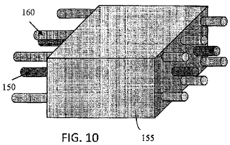
FIG. 10 is a schematic perspective view of an arrangement for forming a
connection with a
pMUT device, according to one aspect of the disclosure;
FIG. 11 is a schematic cross-sectional view of a cable assembly configured to
form a
connection, for example, with the device shown in FIG. 9, according to one
aspect of the
disclosure;
FIG. 12 schematically illustrates a top view of an interposer device
arrangement for
forming a connection with a side-looking two-dimensional pMUT device,
according to another
aspect of the disclosure;
FIG. 13 schematically illustrates an exemplary pMUT device having connective
signal and
ground elements engaged therewith, according to one aspect of the disclosure;
FIG. 14 schematically illustrates a forward-looking ultrasound device,
according to one
aspect of the present disclosure;
FIG. 15 schematically illustrates a side-looking ultrasound device, according
to one aspect
of the present disclosure;
FIG. 16 is a schematic plan view of an arrangement for forming a connection
with a pMUT
device, according to still another aspect of the disclosure;
FIG. 17 is a schematic partial cut away view of the arrangement illustrated in
FIG. 16;
FIG. 18A is a schematic cross-sectional side view of an arrangement for
forming a
connection with a forward-looking two-dimensional piezoelectric micromachined
ultrasonic
transducer device, according to a further aspect of the disclosure;
FIG. 18B is a schematic cross-sectional side view of another arrangement for
forming a
connection with a forward-looking two-dimensional piezoelectric micromachined
ultrasonic
transducer device, according to a further aspect of the disclosure;
- 6 -
CA 02819644 2013-05-31
WO 2012/075153
PCT/US2011/062665
FIG. 19 is a schematic cross-sectional side view of an arrangement for forming
a
connection with a forward-looking two-dimensional piezoelectric micromachined
ultrasonic
transducer device, according to still another aspect of the disclosure;
FIG. 20 is a schematic cross-sectional side view of an arrangement for forming
a
connection with a forward-looking two-dimensional piezoelectric micromachined
ultrasonic
transducer device, according to still yet another aspect of the disclosure;
FIGS. 21 and 22 are schematic end views of pMUT devices (arrays) having ground
electrodes disposed about a periphery thereof with respect to signal
electrodes, according to various
aspects of the disclosure;
FIGS. 23 and 24 are schematic cross-sectional side views of arrangements for
forming a
connection with a forward-looking two-dimensional piezoelectric micromachined
ultrasonic
transducer device, according to various aspects of the disclosure;
FIG. 25A schematically illustrates a forward-looking ultrasound device,
according to one
aspect of the present disclosure;
FIG. 25B schematically illustrates a side-looking ultrasound device, according
to one
aspect of the present disclosure;
FIG. 26 schematically illustrates an exemplary interposer device, according to
one aspect of
the present disclosure;
FIG. 27 schematically illustrates an exemplary interposer device incorporated
into a circuit
board assembly, according to one aspect of the present disclosure;
FIG. 28 schematically illustrates a exemplary component layout for an
ultrasound device
including associated cable assembly and termination element, according to one
aspect of the
present disclosure;
FIGS. 29 and 30 schematically illustrate an exemplary pMUT device (array)
engaged with
a connection support substrate having associated connective signal and ground
elements, according
to one aspect of the present disclosure;
FIGS. 31 and 32 schematically illustrate an exemplary termination element,
such as a
printed circuit board, engaged with a cable assembly having associated
connective signal and
ground elements, according to one aspect of the present disclosure; and
FIG. 33 schematically illustrates the distal end of an exemplary catheter
assembly having a
transducer array, a connection support substrate, and connective signal and
ground elements
disposed in the catheter housing, according to one aspect of the present
disclosure.
- 7 -
CA 02819644 2013-05-31
WO 2012/075153
PCT/US2011/062665
DETAILED DESCRIPTION OF THE DISCLOSURE
The present disclosure now will be described more fully hereinafter with
reference to the
accompanying drawings, in which some, but not all aspects of the disclosure
are shown. Indeed,
the disclosure may be embodied in many different forms and should not be
construed as limited to
the aspects set forth herein; rather, these aspects are provided so that this
disclosure will satisfy
applicable legal requirements. Like numbers refer to like elements throughout.
Aspects of the present disclosure are generally applicable to ultrasonic
transducers, though
particular aspects are particularly directed to a piezoelectric micromachined
ultrasound transducer
("pMUT") having an air-backed cavity. More particularly, aspects of the
present disclosure are
directed to methods of forming an electrically-conductive connection between a
pMUT device and,
for example, an integrated circuit ("IC") and/or corresponding connective
elements, whereby
individual signal and ground leads may extend parallel to the operational
direction of the transducer
array to engage the respective pMUT devices in the transducer array (see
generally, e.g., FIG. 2).
The pMUT device may be disposed within a catheter member 350 having a distal
end or tip 310
(see, e.g., FIGS. 14 and 15). The catheter member 350 may further define a
longitudinally-
extending lumen configured to receive the pMUT device about the distal end
310. The pMUT
device may further comprise a cable assembly 325 comprising connective
elements, and having one
or more connection support substrates 155 disposed about the distal end 310
and proximal end 315
of the catheter.
In such aspects, a representative pMUT or ultrasonic transducer device 270
that may be
implemented in both 1D and 2D transducer arrays, may generally comprise a
plurality of transducer
elements forming a transducer array, wherein each transducer element 272
comprises a
piezoelectric material disposed between a first electrode and a second
electrode, and wherein one of
the first and second electrodes comprises a ground electrode and the other of
the first and second
electrodes comprising a signal electrode. More particularly, as shown, for
example, in FIG. 4, a
transducer element 272 may be disposed on a dielectric layer 274 of a device
substrate 276,
wherein the transducer element 272 includes a piezoelectric material 278
disposed between a first
electrode 280 and a second electrode 282. The primary substrate 284 defines a
first via 286
extending to the device substrate 276, while the device substrate further
defines a second via 288
extending therethrough to the first electrode 280. In some instances, the
first and second via 286,
288 arrangement may extend to the first electrode 280, which is engaged with
the second electrode
282 (shown generally at element 290), thereby connecting the second electrode
282 to the back side
of the substrate. Such an arrangement may be applied, for example, as a back
side ground pad or
ground electrode for the pMUT device 270. In such instances, the first and
second vias 286, 288
- 8 -
CA 02819644 2013-05-31
WO 2012/075153
PCT/US2011/062665
may have a conformal insulating layer 292 deposited therein, before the first
and second vias 286,
288 are substantially filled with first and second conductive materials,
respectively 294, 296. In
some aspects, the first and second electrode engagement 290 may be disposed,
as necessary or
desired about a pMUT array. In some instances, such an arrangement 290 may be
disposed about
the periphery of the pMUT array incorporating the pMUT device structure 270
(see, e.g., FIG. 5),
or in interstices between adjacent pMUT device structures 270 within a pMUT
array (see, e.g., FIG.
9). Such pMUT devices 270 are disclosed, for example, in U.S. Provisional
Patent Application No.
61/299,514 ("Methods for Forming a Micromachined Ultrasonic Transducer, and
Associated
Apparatuses"), assigned to Research Triangle Institute, and which is
incorporated herein in its
entirety by reference.
Particular materials that can be implemented for the piezoelectric material
278 include, for
example, ceramics including ZnO, AIN, LiNbat, lead antimony stannate, lead
magnesium
tantalate, lead nickel tantalate, titanates, tungstates, zireonates, or
niobates of lead, barium, bismuth,
or strontium, including lead zirconate titanate (Pb(ZrxTii,)03 (PZT)), lead
lanthanum zirconate
titanate (PLZT), lead niobium zirconate titanate (PNZT), BaTiO3, SrTiO3, lead
magnesium niobate,
lead nickel niobate, lead manganese niob ate, lead zinc niobate, lead
titanate. Piezoelectric polymer
materials such as polyvinylidene fluoride (PVDF), polyvinylidene fluoride-
trifluoroethylene
(PVDF-TrFE), or polyvinylidene fluoride-tetrafluoroethylene (PVDF-TFE) can
also be used.
One method of forming an electrically-conductive connection with one
configuration of a
pMUT device 270, in the form of a two-dimensional forward-looking pMUT array,
is
schematically illustrated, for example, in FIGS. 6-8. In such instances, the
pMUT device (array)
270 may incorporate a plurality of pMUT elements 272, with the pMUT array
having ground pads
or electrodes 298 (e.g., as associated with the first and second electrode
engagement 290 of the
pMUT device 270, as shown in FIG. 4) arranged about the periphery of the array
such that the
signal pads or electrodes 300 (see, e.g., FIG. 5; as associated with
transducer element 272 of the
pMUT device 270) are arranged within the periphery, for example, in regular
rows. In such
aspects, signal leads (connective elements) and ground leads (connective
elements) extending
parallel to the operational direction of the transducer array may be
configured to form electrically
conductive engagements with the respective ground and signal electrodes 298,
300 of the pMUT
elements 272 within the array, wherein, in some instances, one or more of the
ground electrodes
298 may be common to more than one of the pMUT elements 272 within the array
270.
According to one aspect, as shown in FIGS. 6 and 7, a 2D array of connective
elements
(i.e., wires) may include connective signal elements 150 and connective ground
elements 160, each
of which may or may not be coated with an insulator layer. In one instance, it
may be desirable that
- 9 -
CA 02819644 2013-05-31
WO 2012/075153
PCT/US2011/062665
at least the connective signal elements 150 each be coated with an insulator
layer. In order to form
the electrically-conductive engagement between the connective signal and
ground elements 150,
160 and the respective signal and ground electrodes 300, 298 of the pMUT
device (array) 270, the
connective signal and ground elements 150, 160 may first be arranged such that
first ends thereof
are engaged with and supported by a connection support substrate 155. Such an
engagement may
be accomplished, for instance, using a guide substrate 170 defining a
plurality of parallel, spaced-
apart channels 180 extending across the width thereof (and along the length of
the guide substrate
170), wherein the lateral pitch of the channels 180 generally corresponds to
the lateral pitch of the
connective elements 150, 160 of the pMUT device 270. Once the connective
elements 150, 160 are
inserted into the respective channels 180, so as to extend longitudinally
outward thereof; a retaining
member 190 may be removably applied over the channels 180 so as to retain the
connective
elements 150, 160 within the channels 180. Once prepared, the vide substrate
170 may be
disposed adjacent to the intended connection support substrate 155 (i.e.,
using micropositioners),
and the connective elements 150, 160 directed along the channels 180 to engage
the connection
support substrate 155 for securement therein. The connection support substrate
155 may be, for
example, a silicon substrate with through-holes etched using deep reactive ion
etching (DRIB) to
provide straight (i.e., substantially vertical or otherwise substantially
perpendicular to the plane of
the substrate) sidewalls in the through-holes, which may facilitate high
density arrays of holes (i.e.
without lateral angled sidewalls created by a wet etching process such as KOH
etching). Once
engaged with the connection support substrate 155, the connective elements
150, 160 may be fixed
in the through-holes of the connection support substrate 155 using an adhesive
material such as, for
instance, an insulating epoxy. The free or unengaged surface of the connection
support substrate
155 may then be polished or otherwise planarized to facilitate subsequent
bonding to the pMUT
device 270. Such a process for engaging the connective elements 150, 160 with
a connection
support substrate 155 is disclosed, for example, in U.S. Patent Application
No. 61/329,258
("Methods for Forming a Connection with a Micromachined Ultrasonic Transducer,
and Associated
Apparatuses"), previously been incorporated by reference, and which discloses
other methods for
engaging connective elements with a connection support substrate, as well as
forming an
electrically-conductive engagement between the connective elements and a pMUT
device, a
transducer array, or an intermediate device such as an interposer.
In this regard, the connection support substrate 155, having the connective
signal and
ground elements 150, 160 engaged therewith, may be configured to engage the
pMUT device 270
about the signal and ground electrodes 300, 298, so as to provide, for
example, an appropriate pitch
or spacing of the connective signal and ground elements 150, 160 in
correspondence with the
- 10-
CA 02819644 2013-05-31
WO 2012/075153
PCT/US2011/062665
pMUT device 270, as well as mechanical support for the direct electrically-
conductive engagement
between the connective signal and ground elements 150, 160 and the respective
signal and ground
electrodes 300, 298. As shown in FIG. 8, the connective elements 150, 160 may
thus be assembled
with the connection support substrate 155 such that the connective ground
elements 160 are
disposed about the periphery of the connection support substrate 155 so as to
correspond to the
ground electrodes 298 and to facilitate the formation of the electrically-
conductive connection
therewith. The conductive signal elements 150 are thus disposed within the
periphery of the
connection support substrate 155 So as to correspond to the signal electrodes
300 and to facilitate
the formation of the electrically-conductive connection therewith.
Further aspects of the present disclosure may be directed to a method of
forming an
electrically-conductive connection with another configuration of a pMUT device
270, in the form
of a two-dimensional forward-looking pMUT array, is schematically illustrated,
for example, in
FIGS. 9-11. In such instances, the pMUT device (array) 270 may incorporate a
plurality of pMUT
elements 272, with the pMUT array having the signal pads or electrodes 300
(see, e.g., FIG. 5; as
associated with transducer element 272 of the pMUT device 270) arranged, for
example, in regular
rows, with the ground pads or electrodes 298 (e.g., as associated with the
first and second electrode
engagement 290 of the pMUT device 270, as shown in FIG. 4) arranged in the
interstices of the
signal electrodes 300 of the array (see, e.g., FIG. 9). According to such an
arrangement, the ground
electrodes 298 may be considered interspersed within the regular rows of
signal electrodes 300, or
the rows of ground electrodes 298 may be laterally shifted by about half of
the pitch or spacing
between signal electrodes 300 such that alternating rows of signal electrodes
300 and ground
electrodes 298 are staggered with respect to each other. In such aspects,
signal leads (connective
elements) and ground leads (connective elements) extending parallel to the
operational direction of
the transducer array may be correspondingly configured (see, e.g., FIGS. 10
and 11) to form
electrically conductive engagements with the respective ground and signal
electrodes 298, 300 of
the pMUT elements 272 within the array, wherein, in some instances, one or
more of the ground
electrodes 298 may be common to more than one of the pMUT elements 272 within
the array 270.
As such, one skilled in the art will appreciate that various arrangements of
the connective elements
150, 160 may be required to form the electrically-conductive engagements with
the various
arrangements of pMUT elements 272 within the pMUT device (array) 270.
According to some aspects, the connective elements 150, 160 may be
electrically-engaged
with a side- or lateral-looking transducer array. A representative ultrasound
device implementing a
side- or lateral-looking transducer array is disclosed, for example, in U.S.
Provisional Patent
Application No. 61/419,534 ("Method for Forming an Ultrasound Device, and
Associated
- 11 -
CA 02819644 2013-05-31
WO 2012/075153
PCT/US2011/062665
Apparatus"), filed concurrently herewith, and which is incorporated herein in
its entirety by
reference. In such instances, particularly when the pMUT device (array) is
disposed within a
catheter, the connective elements 150, 160 extend along the catheter, and are
required to engage the
transducer array having the ground and signal electrodes 298, 300 of the pMUT
elements 272
perpendicularly disposed with respect to the longitudinal axis of the
catheter. In such instances, the
connection support substrate 155 may be configured to facilitate navigation of
the change in
direction (i.e., having the channels extending therethrough at an angle of
about 90 degrees with
respect to the longitudinal axis of the catheter). In other instances, the
connective elements 150,
160 may be configured to engage an interposer device 400, as shown, for
example, in FIG. 12,
configured to receive, engage and support an ultrasonic transducer apparatus
(array ¨ not shown)
such that a device plane of the ultrasonic transducer apparatus extends
substantially parallel to the
interposer device 400. In some instances, the interposer device 400 also
includes at least two
conductors 450 extending therealong (i.e., through the interposer device 400
or along a surface
thereof), wherein the conductors 450 each have opposed first and second ends
450A, 450B. One of
the ends 450B may be configured to engage the respective signal and ground
electrodes 298, 300,
in some instances, via wirebond pads such as, for example in a wire bonding
process; while the
other of the ends 450A may be configured to engage the connective signal and
ground elements
150, 160, whether directly or via a connection support substrate.
As shown in FIG. 13, one end of the cable assembly 325, incorporating the
connection
support substrate 155 and the connective signal and ground elements 150, 160,
may be polished or
otherwise planarized (i.e., perpendicularly to the longitudinal axis) so as to
provide a planar surface
for bonding, with an appropriate bonding material 167, the same to the pMUT
device (array) 270.
Thus, the cable assembly 325 may be bonded or otherwise engaged with the pMUT
device 270 in a
number of manners, for example, according to methods and configurations
described, for example,
in U.S. Patent Application No. 61/329,258 ("Methods for Forming a Connection
with a
Micromachined Ultrasonic Transducer, and Associated Apparatuses"), previously
incorporated by
reference. In general, connective elements 150, 160 may be assembled into
connection support
substrates and bonded to transducer arrays / pMUT devices, interposers or
other termination
element, as disclosed, for example, in U.S. Patent Application No. 61/329,258
("Methods for
Forming a Connection with a Micromachined Ultrasonic Transducer, and
Associated
Apparatuses") assigned to Research Triangle Institute (also the assignee of
the present disclosure),
and previously incorporated herein by reference. In some instances, as shown,
for example, in
FIGS. 14 and 15, the cable assembly 325, incorporating the connection support
substrate 155 and
the connective signal and ground elements 150, 160, may be terminated at both
ends 310, 315
- 12 -
CA 02819644 2013-05-31
WO 2012/075153
PCT/US2011/062665
thereof with a connection support substrate, interposer, or other termination
element. More
particularly, one end 310 is configured to engage the pMUT device (array) 270,
whether directly
via a connection support substrate or via an interposer device, while the
opposing end 315 extends
along and/or outwardly of the catheter 350, away from the tip thereof, to
engage a connection
support substrate, interposer, circuit board (i.e., associated with a computer
device), semiconductor
package, or other termination element (see, generally, element 375) configured
to provide external
connectivity between the pMUT device (array) 270 disposed in the catheter 350
and, for example,
an external ultrasound system or other image display device. The connective
elements 150, 160
may be individually assembled at both ends of the cable assembly 325 such that
the connective
elements 150, 160 may be mapped or otherwise tracked with respect to
connectivity to the
transducer elements 272 within the array 270, such that, for instance, the
locations of the transducer
elements within the transducer array can be identified and controlled by the
appropriate electronic
channels in the external ultrasound system.
In light of the aspects previously disclosed, with respect to forming
electrically-conductive
engagements with the pMUT elements 272 in the pMUT array 270, some aspects of
the present
disclosure are further directed to a cable assembly 325 comprising a plurality
of connective signal
elements 150 and a plurality of connective ground elements 160 extending in
substantially parallel
relation along the cable assembly 325, with each being configured to form an
electrically-
conductive engagement with respective ones of the signal electrodes 300 and
the ground electrodes
298 of the transducer elements 272 in the transducer array 270. More
particularly, in some aspects,
the connective ground elements 160 are configured to be alternatingly disposed
(i.e., whether
constructively or actually) with the connective signal elements 150 across the
cable assembly 325,
so as to provide shielding between the connective signal elements 150.
In some instances, as shown, for example, in FIGS. 16 and 17, the cable
assembly 325 may
be configured to provide alternatingly disposed connective ground elements 160
and connective
signal elements 150 (i.e., in actual correspondence with the configuration of
the signal and ground
electrodes 300, 298 of the transducer array 270). That is, the connective
ground elements 160 may
be interspersed among the connective signal elements 150, or otherwise be
disposed between two
or more connective signal elements 150 (i.e., in interstices between adjacent
connective signal
elements 150). The alternatingly disposed connective ground elements 160 and
connective signal
elements 150 (see, e.g., FIG. 11) may further be engaged at opposing ends 310,
315 with
connection support substrates 155, wherein at one such end 310, a connection
support substrate 155
may be engaged with the transducer array 270, in some instances with an
interposer device
disposed therebetween, while the opposing end 315 may have one or more
connection support
- 13 -
CA 02819644 2013-05-31
WO 2012/075153
PCT/US2011/062665
substrates 155 engaged with an interposer, circuit board, semiconductor
package, or other
termination element, as previously disclosed. By actually alternating the
connective ground
elements 160 and the connective signal elements 150, the connective ground
elements 160 may
function as a shield or ground between the connective signal elements 150 in
order, for example, to
reduce cross-talk between the connective signal elements 150 with respect to
signals from the
transducer elements 272. The connective elements 150, 160, comprised of, for
example, relatively
fine gauge wire (e.g., insulated magnet wire having a diameter of between
about 40 AWG and
about 50 AWG), may be individually engaged with the connection support
substrates 155 between
opposing ends so as to provide a registration with respect to the connective
ground and signal
elements 150, 160. In some instances, for example, a color indicia scheme may
be implemented to
distinguish the connective ground and signal elements 150, 160.
In some instances, the connective elements 150, 160 of the cable assembly 325
may be
encapsulated with a dielectric material, such as, for example, a conformal
dielectric coating 320, to
seal and bundle the connective elements 150, 160 to form the cable assembly
325. In other
instances, the connective elements 150, 160 may be wrapped with an outer
covering, such as, for
example, a shrinkable tubing, extending therealong so as to provide a flexible
but robust cable
assembly 325. In further instances, additional shielding for the connective
elements 150, 160 may
be provided, for example, by a conductive film, such as, for example, a metal
foil material 322
(e.g., MYLARO), wrapped about the connective elements 150, 160. The dielectric
coating 320
may be applied to cover the conductive film 322, such that the conductive film
322 is disposed
between the connective elements 150, 160 and the dielectric coating 320. In
other instances (not
shown), a conductive film may be wrapped about the dielectric material 320, so
as to be disposed
between the catheter member 350 and the dielectric material 320 encapsulating
the connective
signal and ground elements 150, 160. In either instance, the conductive film
322 may provide
additional shielding for at least the connective signal elements 150, 160.
Still in other instances,
additional shielding may be molded or otherwise incorporated into the catheter
member 350 such
as, for example, a metal braid (not shown) molded into the catheter member
350.
In some aspects, the ground electrodes 298 arranged about the periphery of the
transducer
array 270 may be much less than the number of transducer elements 272 (and
thus the
corresponding number of signal electrodes 300) in the array 270. For example,
a 20x20 transducer
array with 125 pm pitch may yield a transducer array of about 2.5 mm in width.
In such an
instance, a catheter size of 10 French (2.8 mm I.D.) would be needed. Thus,
only one ring of
ground electrodes 298 could be disposed about the periphery of the transducer
array, resulting in a
22x22 array with an overall width of about 2.75 mm. As such, the arrangement
would include 400
- 14 -
CA 02819644 2013-05-31
WO 2012/075153
PCT/US2011/062665
transducer elements 272 (corresponding to 400 signal electrodes 300 disposed
within the periphery)
and 84 ground electrodes 298. If corresponding connective signal and ground
elements 150, 160
are incorporated into the corresponding cable assembly 325, the relatively few
connective ground
elements 160 may not necessarily provide adequate shielding for the connective
signal elements
150. As such, further aspects of the present disclosure are directed to other
arrangements, whether
actual or constructive, wherein the connective ground elements 298 of the
cable assembly 325 are
alternatingly disposed or otherwise interspersed with respect to the
connective signal elements 150
along the length of the cable assembly 325. One skilled in the art will
appreciate that other
arrangements may be provided in order to increase the ratio of ground to
signal wires without
increasing one or both lateral dimensions of the transducer array. For
example, as shown in FIG.
21, additional columns of connective ground elements 298 may be arranged only
along one axis of
the transducer array 270 adjacent to the connective signal elements 300. More
particularly, such an
arrangement may include, for example, a 20x26 array containing 400 connective
signal elements
and 120 connective ground elements, or a 20x40 array containing 400 connective
signal elements
and 400 connective ground elements. In another aspect, for instance, the
corners of the array can
be implemented as connective ground elements 298 in order to maintain array
size along both
cross-sectional axes. More particularly, for example, the 20x20 array shown in
FIG. 22 may be
configured to include 340 connective signal elements and 60 connective ground
elements.
In this regard, as shown in FIG. 18A, the connective signal elements 150 and
connective
ground elements 160 may be intermingled such that the connective ground
elements are
substantially or constructively alternatingly disposed or otherwise
interspersed with respect to the
connective signal elements 150, regardless of the position in which the
respective connective
ground element 160 interacts with the termination element (i.e., connection
support substrate 155).
That is, in instances where the connective ground elements engage the
termination element (i.e.,
connection support substrate 155) about the periphery thereof, the respective
connective ground
elements 160 may be routed between the connective signal elements 150 at least
partially along the
length of the cable assembly 325 (i.e., from the periphery about the first
termination element, along
the cable assembly 325 at an interstitial site, and back to the periphery
about the opposing second
termination element). Further, in some instances, the connective signal
elements 150 and
connective ground elements 160 may be twisted (i.e., in pairs or larger number
of such elements)
together, at least partially along the length of the cable assembly 325, as
another manner of routing
the connective ground elements 160 between the connective signal elements 150
at least partially
along the length of the cable assembly 325. Further, as shown in FIG. 18B,
additional connective
ground elements 165 may be attached or otherwise incorporated in to the cable
assembly 325 using,
- 15-
CA 02819644 2013-05-31
WO 2012/075153
PCT/US2011/062665
for example, a conductive epoxy 306 applied to the support substrate 155
and/or otherwise to the
cable assembly 325, wherein such additional connective ground elements 165 may
be further
interspersed between the connective signal elements 150. Such additional
connective ground
elements 165 may further be inserted into the connection support substrate
155, or may be separate
elements, externally-attached using, for example, a conductive epoxy material.
The additional
connective ground elements 165 may be, for instance, individual wires, strips
of metal foil, and/or
other conductive material interspersed between the connective signal elements
(i.e., wires) to
provide additional shielding therefor.
In another aspect, as shown in FIG. 19, the connective signal elements 150 may
be insulated
along the length of the cable assembly 325, while the connective ground
elements may be bare, or
at least partially bare, conductive material (i.e., bare or partially bare
copper wire). In such
instances, a conductive epoxy material 306 may be applied to the connective
elements 150, 160 so
as to extend between the collective elements 150, 160 and collectively
encapsulate the connective
elements 150, 160. The conductive epoxy material 306 may extend along the
cable assembly 325
between the opposed ends, as shown in FIG. 19, or only partially along the
length of the cable
assembly 325, as shown in FIG. 20. The conductive epoxy material 306 may be,
for example, a
silicone, a urethane-based epoxy or other flexible epoxy filled with
conductive particles or
otherwise having conductive particles incorporated therein, or other suitable
material, wherein such
epoxy materials may promote or facilitate flexibility of the cable assembly
325. Further, such a
conductive epoxy material 306 may form an electrically-conductive engagement
with the
connective ground elements (bare or partially bare conductive material) 160 so
as to essentially
form a single conductive body extending about and between all connective
signal elements 150.
Such a configuration thus constructively facilitates connective ground
elements 160 that are
alternatingly disposed with respect to the connective signal elements 150
along the cable assembly
325.
According to another aspect, the connective signal elements 150 may be coated
with a
conductive coating material applied to each such elongate insulated element
extending along the
cable assembly 325. In such instances, the connective ground elements 160 may
be at least
partially in electrically-conductive communication with the connective signal
elements 150 via the
conductive coating material, thus also constructively facilitating connective
ground elements 160
that are alternatingly disposed with respect to the connective signal elements
150 along the cable
assembly 325. For example, a conformal thin film copper layer may be deposited
on the insulator
material covering the connective signal elements 150 by metal organic chemical
vapor deposition
(MOCVD), electroless plating, or a conductive spray process. Such a coating
may form a coaxial
- 16 -
CA 02819644 2013-05-31
WO 2012/075153
PCT/US2011/062665
conductor configuration for each connective signal element 150, such that this
outer coating may be
electrically-connected to the connective ground elements 160 via the
conductive epoxy 306 applied
thereto, thus providing additional shielding around each connective signal
element 150. Coating
the connective signal elements 150 with a conductive substance may further
facilitate increased
flexibility of the cable assembly 325 by allowing the conductive epoxy
material 306 to be applied
only partially along the length of the cable assembly 325, as shown in FIG.
20. In such an aspect,
the conductive epoxy material 306 may be applied to the connective elements
150, 160 proximate
to the connection support substrates 155 and not along the entire length of
the cable assembly 325.
Such a configuration constructively facilitates connective ground elements 160
that are
alternatingly disposed with respect to the connective signal elements 150
about the connection
support substrates 155 by way of the conductive epoxy material 306, while such
alternating
disposition of the connective ground elements 160 is otherwise facilitated by
the conductive
coating material applied to the connective signal elements 150 (i.e., by way
of conductive physical
contact between the conductive coating material and the bare conductive
material of the conductive
ground elements 160) along the length of the cable assembly 325 free of the
conductive epoxy
material 306.
The cable assemblies shown in FIGS. 16-20 are exemplary cable assemblies for
forward-
looking 1D or 2D arrays as shown, for instance, in FIG. 14. In another aspect,
similar cable
assemblies can be configured, for example, as shown in FIG. 23, for side-
looking 1D and 2D
arrays, as shown in FIG. 15. In such instances, the connection support
substrate 255 bonded to or
otherwise engaged with the transducer array 270 may be configured to
facilitate a change in
direction of the connective signal and ground elements 150, 160 extending
longitudinally along the
catheter to a mating arrangement for the transducer array 270, wherein such a
mating arrangement
may be oriented perpendicularly to the longitudinal axis of the catheter. Once
engaged with the
mating arrangement, the signal and ground wires (the connective signal and
ground elements) can
then be bent approximately 90 degrees to extend the connective elements
substantially parallel with
the longitudinal axis of the catheter. Such a configuration of the cable
assembly may thus also
facilitate bending of the connective signal and ground elements, for example,
in comparison to a
multiple level flex cable arrangement that may be relatively stiffer and more
difficult to bend
without risk of damage to the flex cable assembly. For the assembly shown in
FIG. 23, each
individual conductor wire (conductive element) may have a relatively small
diameter (e.g., between
about 40 AWG and about 50 AWG), and may thus be relatively flexible and
readily bent at about a
90 degree angle. The bent conductors may then be, for example, encapsulated by
an epoxy material
such as, for example, a potting epoxy 400, as shown in FIG. 25B, to provide
stiffness and/or strain
- 17 -
CA 02819644 2013-05-31
WO 2012/075153
PCT/US2011/062665
relief for the conductors, adjacent to the connection support substrate 255
attached to the transducer
array 270 disposed at the distal end 310 of the catheter member 350.
In some instances, the distal end 310 of the catheter member 350 may also
include a fluid-
containing or fluid-filled capsular member 410, as shown in FIGS. 25A and 25B,
configured to
house at least the pMUT device 270. The fluid contained within the capsular
member 410 may, for
example, facilitate acoustic transmission of the acoustic energy emitted by
the pMUT device 270
through the catheter wall and into the body or fluid bed of the organ being
imaged, for example, the
heart or a vessel. Some standard or existing piezoelectric ultrasound
transducers may be embedded
in an epoxy material to facilitate acoustic transmission via an epoxy matching
layer. However,
pMUT devices according to aspects of the present disclosure include flexible
transducer
membranes (i.e., piezoelectric material 278) that are preferably configured
and arranged to avoid
mechanically loading or constraint by a mechanical impediment such as an epoxy
layer. Thus, the
fluid medium contained within the capsular member 410 and in contact with the
pMUT transducer
array 270 may provide an advantageous configuration for improve signal
transmission and imaging
capabilities. The fluid contained within the capsular member 410 may comprise,
for instance,
silicone or other fluid with appropriate viscosity, for example, between about
1 cSt and about 100
cSt, and/or appropriate acoustic impedance, for example, between about 1 MRayl
and about 1.5
MRayl, or less than about 5 MRayl. Once formed, the pMUT device 270 having the
connection
support substrate 255 engaged therewith may be inserted into the lumen of the
catheter and, in turn,
into the capsular member 410 disposed about the distal end 310 of the
catheter. In other aspects,
the capsular member 410 may be engaged with the distal end 310 of the
catheter, externally or
substantially externally to the lumen of the catheter. The capsular member 410
may then be filled
or substantially filled with the appropriate fluid, and the capsular member
then be sealed, whether
about the cable assembly 325 or otherwise, using, for example, heat or epoxy,
to form a fluid tight
seal. In some aspects the capsular member 410 may be sealed to as to contain
at least the pMUT
device 270. However, in some instances, the capsular member 410 may be sealed
about the
connection support substrate 255 engaged with the pMUT device 270, about the
epoxy material
(i.e., potting epoxy 400), if present, applied to the connective elements of
the cable assembly 325
adjacent to the connection support substrate 255, or about the cable assembly
325 itself.
At the proximal end 315 of the catheter 350, the connection support substrate
355 of the
cable assembly 325 may be engaged with or otherwise terminated by a
termination element 375,
such as, for example, an interposer, circuit board or semiconductor package.
In this regard, the
distal end connection support substrate 255 may have a pitch of the connective
signal and ground
elements 150, 160 that is approximately the same as the transducer array 270
in order to facilitate
- 18-
CA 02819644 2013-05-31
WO 2012/075153
PCT/US2011/062665
bonding and electrical engagement of the connective elements to the pMUT array
270. Such a
relatively fine pitch may also facilitate extension of the connective elements
substantially parallel
(or first bent at about 90 degrees and then extension substantially parallel)
to the longitudinal axis
of the catheter in a close-packed configuration. Such an arrangement may, for
instance, allow
several hundred conductors to fit within a small, for example, 3 mm diameter,
catheter 350. About
the proximal end 315 of the catheter 350, the connective signal and ground
elements 150, 160
engaged with the connection support substrate 355 may be configured to
electrically-engage
corresponding conductor elements associated with a termination element 375
such as, for example,
an interposer, circuit board or semiconductor package. Such conductor elements
may comprise, for
example, metal conductors deposited by electroplating, RF sputtering or
evaporation, and patterned
on the surface of the termination element 375. The conductor elements of the
termination element
375 may, for example, facilitate an electrically-conductive engagement between
the connective
signal and ground elements 150, 160 associated with the connection support
substrate 355, and, for
instance, a connector cable for the ultrasound system, solder bumps attaching
additional circuitry
by flip chip bumping, or other devices configured to facilitate generation of
the ultrasound image
by an external device or system. In another aspect, such an arrangement may be
advantageous, for
example, by providing a cable assembly 325 having a relatively lower materials
cost. For example,
insulated magnet wire may cost approximately $0.004 per meter length, whereas
some flex cables
containing 16 conductors may cost approximately $10 per meter length. Thus,
for 256 conductors
in a 1 meter length catheter, magnet wire may cost about $1 per catheter,
whereas flex cable could
cost about $160 per catheter. Such an example thus illustrates the magnitude
of the cost savings
that may be realized according to various aspects of the present disclosure.
In some instances, the pitch of the connective signal and ground elements 150,
160 may be
increased in order to facilitate engagement with the termination element 375
and, in turn,
engagement between the termination element 375 and the external ultrasound
system. For
example, routing 400 connective signal elements (20x20 array) with respect to
an interposer device
having an element pitch of between about 100 microns and about 200 microns may
be difficult
without requiring conductor traces on the interposer device to be extremely
narrow and close
together. Such a configuration could undesirably cause cross talk between
conductor traces, as well
as increased ohmic resistance thereof, which could degrade the signals carried
thereby. An
example of such a termination interposer device 500 is shown, for example, in
FIG. 26, wherein
such an interposer device 500 includes a 20x20 array of signal pads 510 for
engaging the
connective signal elements 150. Such signal pads 510 are routed through signal
traces 520 to
connection pads 530, wherein the interposer device can then be electrically-
connected through the
- 19-
CA 02819644 2013-05-31
WO 2012/075153
PCT/US2011/062665
connection pads 530, via wirebonding or solder bumping, for example, to a
circuit board or other
semiconductor package. In instances where the spacing between the signal pads
510 is about 75
um, the pitch of the signal traces 520 may be as small as about 16 um, with
the width of the signal
traces 520 being as small as about 8 um, and the length of the signal traces
520 being at least
several millimeters from the signal pads 510 to the connection pads 530
disposed about the edges
of the interposer device. The 20x20 array may be about 4 mm in width, while
the interposer device
may have a width of about 17 mm. Further, as many as 4 signal traces 520 may
be routed between
signal pads 510. Such a relatively fine pitch and relatively narrow trace
width could thus carry the
risk of causing signal degradation.
As such, according to some aspects, an arrangement for termination of the
connection
support substrate 355 is shown, for example, in FIGS. 24 and 27. In such
aspects, the main cable
assembly 325, containing several hundred conductors, can be divided into
smaller cable
subassemblies 330 near the proximal end 315, as shown, for example, in FIG.
24. For example, a
cable assembly 325 with 600 conductors can be divided into 8 subassemblies 330
containing 75
conductors each, with each subassembly 330 toward the proximal end 315 having
its own
termination connection support substrate 355. Each subassembly 330 may be
bonded to an
individual interposer device 610 configured as shown, for example, in FIG. 27.
As shown in FIG.
27, a termination circuit board 600 may include routing to connect termination
interposer devices
610 to connectors 620 for a cable extending to the external ultrasound system.
For example, for a
cable assembly 325 having 512 signal wires (connective signal elements), each
termination
interposer device 610 may include, for example, 64 signal traces. One or more
interposer devices
610 can be connected to connection pads 630 on the termination circuit board
600, for instance, via
wirebonding, by solder bumping, or by mounting the interposer devices 610 into
semiconductor
packages (not shown) that are connected to the termination circuit board 600.
The routing
associated with the termination circuit board 600 may then be implemented to
electrically engage
the signal traces to the connector 620 associated with the external ultrasound
system. In such
instances, signal trace routing associated with the interposer device 610 can
be accomplished with
relatively shorter traces, relatively wider signal traces, and relatively
larger pitch, thus reducing or
otherwise eliminating signal degradation.
An exemplary overall schematic of a component layout for a pMUT array 270 with
associated cable assembly and termination element is shown in FIG. 28. The
transducer array 270
may be bonded to the distal connection support substrate 255 having the
connective signal and
ground elements 150, 160 (not shown) engaged therewith using, for example,
solder bumps, gold
stud bumps or an anisotropic conductive epoxy, to provide an electrically-
conductive connection
- 20 -
CA 02819644 2013-05-31
WO 2012/075153
PCT/US2011/062665
between the pMUT array elements and the connective signal and ground elements
(wires) 150, 160.
The connective elements extend as part of the cable assembly (not shown) to
the proximal
connection support substrate(s) 355 (i.e., the termination). The connection
support substrates 355
may then be bonded to the termination interposer devices 610 using, for
example, solder bumps,
gold stud bumps or an anisotropic conductive epoxy, to provide an electrically-
conductive
connection between the connective signal and ground elements (wires) 150, 160,
and the signal
pads 510 of the respective interposer device 610. The interposer routing 520
subsequently provides
an electrically-conductive connection to the connection pads 530 of that
interposer device 610,
which may then, in turn, be wirebonded or otherwise electrically connected to
the connection pads
630 of a termination PC board 600 associated with the external ultrasound
system. In other aspects,
the interposer devices 610 may be wirebonded into semiconductor packages 640
that may be
mounted onto termination PC boards 600 using, for example, electrically
conductive pins or solder
bumps. In still other aspects, the interposer devices 610 may instead include
through-silicon vias or
through-substrate vias substantially filled with a conductive material,
wherein such vias, or other
conductive traces associated with the interposer device 610, may be attached
to connection pads
530 on the termination PC board 600, for instance, via solder bumps, gold stud
bumps, or an
anisotropic conductive epoxy. The termination PC board 600 further routes the
connections with
the connective elements from the interposer device to the connector 620
associated with a cable
650 extending to the external ultrasound system. In some instances, the
termination PC board 600
may also include other circuitry to facilitate forming of an ultrasound image,
for example, transmit
pulsers, transmit beamformers, amplifiers, receive beamformers,
transmit/receive switches, timing
circuits, and other appropriate circuitry and/or components, as will be
appreciate by one skilled in
the art.
Aspects of a cable assembly 325 as disclosed herein may be implemented, in
some
instances, with other types of appropriately-configured ultrasound
transducers, as will be
appreciated by one skilled in the art. Such an appropriately configured
ultrasound transducer may
comprise, for example, a PZT ceramic ultrasound transducer with signal and/or
ground electrodes
on at least one side of the transducer array for connection to a connection
support substrate of the
cable assembly 325. In another aspect, such an ultrasound transducer may
comprise, for instance, a
capacitive micromachined ultrasound transducer (cMUT), that may include
through-silicon or
through-substrate vias for providing electrically-conductive connections with
the back side of the
substrate, may be bonded to a connection support substrate of the cable
assembly 325. Thus, a
cable assembly 325 according to aspects of the present disclosure may be
implemented with many
other types and configurations of ultrasound transducers to facilitate the
connection of a relatively
-21 -
CA 02819644 2013-05-31
WO 2012/075153
PCT/US2011/062665
large number of connective signal and ground elements in a relatively small
diameter probe, such
as a catheter or endoprobe. In some exemplary instances, pMUT arrays or other
transducer arrays
assembled with such cable assemblies may be advantageous in catheters or other
probes having a
relatively small diameter and a relatively high number of transducer elements,
for instance, for use
in interventional cardiology or interventional radiology applications, such as
intravascular or
intracardiac surgical procedures. In other instances, such transducers and
cable assemblies may be
advantageous in other types of endoprobe devices having a relatively small
diameter and a
relatively high number of transducer elements, such as laparoscopic ultrasound
probes used for
minimally invasive surgeries, such as prostate, liver or gall bladder
procedures.
Many modifications and other aspects of the disclosures set forth herein will
come to mind
to one skilled in the art to which these disclosures pertain having the
benefit of the teachings
presented in the foregoing descriptions and the associated drawings. For
example, one such aspect
of an ultrasound transducer with associated cable assembly may be provided in
instances where the
transducer and cable assembly are configured for use in a side-looking
intracardiac catheter, having
an outer diameter of about 14 French (about 4.6 mm). More particularly, a pMUT
array may be
fabricated with 512 transducer (pMUT) elements 272 (i.e., a 16x32 array) and
96 ground pads or
electrodes 298, generally configured as shown, for example, in FIG. 4. As
disclosed, the pMUT
array may be configured such that the structure of the pMUT elements 272
includes through-
substrate vias/interconnects, so as to provide electrically-conductive
connections to the ground and
signal electrodes 298, 300 of the pMUT elements 272 within the array on the
back side of the
substrate. The pitch of the pMUT elements in the pMUT array may be on the
order of about 175
im for an overall array size of about 2.8 mm x 5.6 mm. The 2.8 mm array width
is configured to
fit within the lumen of a 14 French catheter (inner diameter of about 3.8 mm).
Such a pMUT array
is thus configured to be capable of real-time 3D ultrasound imaging. As a
result of such a
configuration, one signal conductor is required per pMUT element in the pMUT
array in order to
allow the pMUT elements to be individually actuated. However, this arrangement
results in a
relatively higher number of required conductors in the cable assembly than
conventional flex cable,
micro-coax cable or micro-ribbon cable can provide in a sufficiently small
form factor for
implementation in an intracardiac catheter. Conventional 2D linear array
devices used in
ultrasound catheters typically include only 64 transducer elements; therefore,
conventional cabling
can be used in such instances.
Accordingly, in order to overcome the noted limitations of conventional
cables, while
meeting the noted requirements, one exemplary aspect may be directed to a
cable assembly, as
shown in FIG. 29, including on the order of 512 connective signal elements and
128 connective
- 22 -
CA 02819644 2013-05-31
WO 2012/075153
PCT/US2011/062665
ground elements. However, in some instances, the cable assembly may include at
least 100
connective signal elements though, in other instances, the cable assembly may
include at least 400
connective signal elements, consistent with the principles discussed in
relation to the these and
other aspects of the disclosure. In such an aspect, the connection support
substrate 155 may be
comprised, for example, of silicon or any other suitable material, in which
vias may be etched
therethrough using, for instance, a DRIE process. The connective signal and
ground elements may
then be directed/inserted into the etched vias in a connection support
substrate in correlation with
the pattern of transducer elements and ground pads in the pMUT array. The
connective signal and
ground elements may be on the order of between about 40 AWG and about 50 AWG
in diameter,
wherein, in one instance, the connective signal and ground elements may be 45
AWG insulated
magnet wire. For differentiation/distinction during formation of the cable
assembly, the connective
signal elements 150 may be configured to have red insulation, while the
connective ground
elements 160 may be configured to have clear, white, or any other suitable
color insulation
distinguishable from the insulation of the connective signal elements. In some
instances, the pitch
of the vias/through-holes in the connection support substrate may be on the
order of less than 200
microns though, in other instances, the pitch may be on the order of less than
about 100 microns.
In one particular aspect, the pitch about 175 um to correspond to the pitch of
the connections for
the pMUT array 270 previously disclosed. The connective signal and ground
elements may be
secured in the vias of the connection support substrate using, for example, a
low-viscosity
insulating epoxy material or any other suitable bonding material. In any
instance, the surface of the
connection support substrate configured to engage the pMUT array 270 may first
be polished to
expose the ends of the connective signal and ground elements extending
therethrough and to
provide a flat surface for bonding to the pMUT array. The pMUT array and
connection support
substrate may be bonded together, for example, using an epoxy material,
wherein the exposed ends
of the connective signal and ground elements are in electrically-conductive
engagement with the
signal and ground contacts on the back side of the pMUT array. FIG. 29 shows
one example of a
pMUT array 270 bonded to a connection support substrate 155 with associated
connective signal
and ground elements (i.e., wires) 150, 160, as previously disclosed. The
wires, proximate to the
ends thereof, may also be individually bent at an angle of about 90 degrees to
provide a side-
looking catheter configuration as shown, for example, in FIG. 23. Because the
cable is made of
individual wires, there may be little or no mechanical stress on the
conductors, compared to
bending a flex cable assembly (e.g., as shown in FIG. 1), wherein such bending
may impart
significant stress on the collective flex cable assembly.
- 23 -
CA 02819644 2013-05-31
WO 2012/075153
PCT/US2011/062665
The connective ground elements may be connected to the ground contacts of the
pMUT
array laterally outward of the connective signal elements as shown, for
example, in FIG. 21.
Additional connective ground elements (wires) 165 may be provided in the cable
assembly over the
number of available ground contacts in the pMUT array, for example, to provide
additional
shielding of the connective signal elements, as shown, for instance, in FIG.
30 (see also, e.g., FIG.
18B), wherein in one aspect, a total of 128 ground wires may be provided in
the cable assembly for
connection to the ground contacts of the pMUT array and to shield the 512
connective signal
elements in the cable assembly. In such instances, for example, every 4
connective signal elements
(wires) may be twisted together with one connective ground element (wire) in
the cable assembly
to facilitate shielding of the connective signal elements by interspersing the
connective ground
elements among the connective signal elements. Sheathing, such as shrink
tubing 320 may be
provided and installed about the connective elements of the cable assembly so
as to provide a more
robust sheathed cable assembly 325. In some aspects, the connective elements
of the cable
assembly may be terminated opposite to the connection support substrate by a
termination element
such as, for example, a printed circuit board (PCB) 375 as shown in FIG. 31.
The PCB itself may
also include a connector 620 for forming an electrically-conductive connection
with an ultrasound
system. The conductive signal and ground elements 150, 160 may be engaged
(i.e., soldered) with
conductively-plated vias 151 in the PCB 375 as shown, for example, in FIG. 32.
There may be, for
example, between one and eight PCB's engaged with the free ends of the
connective signal and
ground elements of the cable assembly, opposite to the connection support
substrate, as necessary
or desired, depending, for instance, on the number of connective signal and
ground elements in the
cable assembly and the number of pinouts on the respective PCB, though the
number of PCB's may
vary considerably.
The cable assembly 325 shown, for example, in FIG. 31, may have a length of
about 50" for
implementation in a 36" length intracardiac catheter. The distal end of a 14
French catheter
assembly is shown, for example, in FIG. 33, with the transducer array 270,
connection support
substrate 155 and connective signal and ground elements 150, 160 visible in
the distal tip of the
catheter assembly. The catheter housing may be comprised of Pebax0 with
embedded metal
braiding. In some instances, the catheter housing may include a marker band
for facilitating
visualization of the tip under fluoroscopy and/or a pull wire to deflect the
catheter tip (i.e., catheter
control/steering). In particular aspects, the catheter assembly may be
particularly configured for
real-time 3D intracardiac ultrasound imaging. For example, the catheter
assembly may be placed in
the right atrium via the inferior vena cava for imaging an ablation catheter
in the left atrium during
a pulmonary ablation procedure.
- 24 -
CA 02819644 2013-05-31
WO 2012/075153
PCT/US2011/062665
Other examples of transducer and cable assemblies, such as disclosed in the
present aspect,
may be used for intravascular imaging. In such instances, the catheter
assembly may be required to
have a relatively smaller outer diameter, for example, of no more than about 6
French (about 2
mm). In order to meet the size constraints of the catheter assembly, the
transducer array may have
fewer elements and, as such, the corresponding cable assembly may have fewer
signal wires that
must fit within the inner diameter of the catheter. For example, in such
instances, the size
constraint may be met by a transducer array of 256 pMUT elements (16x16
transducer array), with
a pMUT element pitch of about 60 microns, and with the cable assembly
including 256 connective
signal elements and 64 connective ground elements. In such a configuration,
the connection
support substrate would require a via pitch of about 60 microns to correspond
with the signal and
ground contact pitch of the transducer array, so as to facilitate an
electrically-conductive
engagement therebetween. In some instances, the connective signal and/or
ground elements (wires)
may be configured with a relatively smaller diameter, e.g., between about 45
AWG and about 50
AWG, so as to reduce, or further reduce, the lateral dimension of the cable
assembly. Such an
intravascular catheter could be used, for example, for real-time 3D ultrasound
imaging of a stent
placed in an artery or for imaging an occlusion in an artery. Accordingly,
such a catheter assembly
may be appropriately scaled, for example, so as to be configured to fit within
a 2 mm catheter (i.e.,
with >100 connective signal elements at a pitch of <100 um for intravascular
ultrasound
applications), or to fit within a 3-4 mm catheter (i.e., with >400 connective
signal elements at a
pitch of <200 um for intracardiac echo applications).
Therefore, it is to be understood that the disclosures are not to be limited
to the specific
aspects disclosed and that modifications and other aspects are intended to be
included within the
scope of the appended claims. Although specific terms are employed herein,
they are used in a
generic and descriptive sense only and not for purposes of limitation.
- 25 -