Note: Descriptions are shown in the official language in which they were submitted.
CA 02820862 2013-06-07
WO 2012/077084 PCT/1B2011/055576
1
DETONATION OF EXPLOSIVES
FIELD OF THE INVENTION
This invention relates to detonation of explosives. More particularly, the
invention
relates to detonator systems for detonating explosives with which they are
arranged in
a detonating relationship. The invention accordingly provides a detonator
system for
detonating an explosive charge with which it is, in use, arranged in a
detonating
relationship. The invention also provides a method of operating a detonator
system.
The invention further provides a shock tube.
BACKGROUND TO THE INVENTION
Detonation of explosive charges is generally effected by means of detonators
which
are provided in a detonating relationship with the explosive charges. Such
explosive
charges usually comprise so-called "main" or "secondary" explosives.
In the mining industry, in particular, as well as in a number of other
industries which
rely on the use of explosives, e.g. the demolition industry, accurate control
of
CA 02820862 2013-06-07
WO 2012/077084 PCT/1B2011/055576
2
explosives detonation is of great importance, for reasons including safety and
accuracy of blasting operation.
Generally speaking, one can distinguish between two types of detonators namely
electronic detonators and pyrotechnic detonators.
Electronic detonators generally effect detonation of an explosive with which
they are in
a detonating relationship by generating a voltage spark or plasma in proximity
to the
explosive. Such voltage spark or plasma is generated by the breakdown of a
resistive
element or bridge which is provided between two conductive electrodes. The
resistive
bridge and the electrodes are generally referred to collectively as a "fuse
head" which
is accommodated within a detonator housing. The plasma generates a shock wave
which is transmitted to the proximate explosive and initiates the explosive.
Such electronic detonators generally provide accurate control over detonation,
particularly as regards timing and delay properties thereof. However,
electronic
detonators are expensive to manufacture and difficult to use usually also,
requiring a
separate or external power source and complex electronic transmission wire
connections to allow transmission of electricity to the detonator and permit
remote
triggering thereof. In the applicant's experience, such detonator connections
are
prone to failure and may even result in premature initiation of the detonator
and thus of
the explosive, possible due to false stimuli, e.g. radio-frequency (RF)
interference on
the mining/demolition site.
CA 02820862 2013-06-07
WO 2012/077084 PCT/1B2011/055576
3
In contrast to electronic detonators operating by means of an electronic delay
system,
pyrotechnic detonators employ a series of explosive charges that are located
within a
detonator housing to provide a desired detonating signal to the main explosive
charge
at a required timing and delay. The series of explosive charges generally
includes (i)
an initiating and sealing charge, also known as a priming charge, (ii) a
timing charge,
(iii) a primary charge and, optionally, (iv) a base charge. The initiating
charge serves
to initiate the explosive sequence in response to a shock signal transmitted
thereto
and also functions as a sealing charge which provides a seal to prevent blow-
back
inside the detonator housing. The initiating charge also initiates the timing
charge
which provides a desired burning delay for detonation. The timing charge, in
turn,
initiates the primary charge which either directly provides a detonation
initiating signal
to the main explosive charge, or initiates the base charge that, in turn, will
provide the
desired detonation initiating signal to the main explosive charge.
As alluded to above, initiation of the initiating charge of a pyrotechnic
detonator is
generally effected by imparting a shock signal to the detonator, typically
being
provided by one or more shock tubes which are located in an initiating
relationship with
the detonator. The initiating charge then typically comprises a sensitive
explosive,
initiation of which can be effected by a shock wave of sufficient magnitude.
Shock
tube is well known and widely used in the initiation of detonators; it
comprises a hollow
plastic tube lined with a layer of initiating or core explosive, typically
comprising a
mixture of HMX and aluminium metal powder. Upon ignition of the initiating
(core)
explosive, a small explosion propagates along the tube in the form of an
advancing
temperature/pressure wave front, typically at a rate of approximately 7000
ft/s (about
2000rn/s). Upon reaching the detonator, the pressure/temperature wave triggers
or
CA 02820862 2013-06-07
WO 2012/077084 PCT/1B2011/055576
4
ignites the initiating/sealing charge in the detonator, which results in the
sequence of
ignitions mentioned above and thus eventually causing detonation of the main
explosive charge. Although shock tube is economically attractive and easy to
use,
existing pyrotechnic-based detonator systems do not at all permit the same
extent of
control of detonation timing and delay which is achieved by using electronic
detonators, as the timing and delay features are provided by the detonator
explosive
charge loading, instead of by electric components.
The present invention therefore seeks, broadly, to provide an approach to
operating
explosive detonators which addresses and at least partly alleviates the
disadvantages
associated with both pyrotechnic and electronic initiation of explosive
detonators.
SUMMARY OF THE INVENTION
In accordance with a first aspect of the invention, there is provided an
explosives
detonator system for detonating an explosive charge with which it is, in use,
arranged
in a detonating relationship and which, on operative acceptance of a
detonation
initiating signal that has a detonation initiating property, is capable of
initiating and thus
detonating the explosive charge, the detonator system including
an initiating device which is capable of accepting the detonation initiating
signal
and of initiating and thus detonating the explosive charge, the initiating
device being in
a non-detonation initiating condition in which it cannot operatively accept
the
detonation initiating signal and thus assume a detonator initiating condition
when the
detonation initiating signal is transmitted thereto; and
CA 02820862 2013-06-07
WO 2012/077084 PCT/1B2011/055576
a switching device that is capable of detecting a chemical compositional
component as a switching property of a switching signal that is transmitted to
the
detonator system, with the switching device being capable of switching the
initiating
device, on detection of the chemical compositional component, to a standby
condition
5 in which the initiating device is capable of operatively accepting the
detonation
initiating signal when it is transmitted thereto.
For the purposes of continuity with the wording used in the specification of
priority
application number ZA 2010/08925, it is to be noted that the initiating device
is, in
effect, a trigger for a detonator and, in a sense, comprises a detonator. The
switching
device, in turn, is, in effect, a detector or sensor. Similarly, the switching
property is a
triggering property and the switching signal an initiating signal. Further
differences in
terminology between the specification of priority application number ZA
2010/08925
and the present specification will be apparent from the description that
follows.
It will be appreciated that the presence of the chemical compositional
component in
the switching signal is therefore a prerequisite for the initiating device to
become
susceptible, by being switched into the standby condition, for being switched
into the
detonation initiating condition.
The switching signal may, in particular, be a shock signal which is provided
by, and
propagated along, shock tube. The system may then include shock tube that is
arranged or provided in initiating proximity to the initiating device. The
chemical
compositional component may then, in particular, be provided by a product wave
component of the shock signal, comprising product gases resulting from
progressive
CA 02820862 2013-06-07
WO 2012/077084 PCT/1B2011/055576
6
detonation of an explosive substance contained in the shock tube. In one
embodiment
of the invention, the shock tube may contain a tracer compound, combustion of
which,
due to detonation of the explosive substance, releases a product gas that
constitutes
the chemical compositional component. Alternatively, the chemical
compositional
component may be a normal product gas of the explosive substance.
The shock tube may, in particular, be a shock tube as is hereinafter
described, having
a hollow elongate body, inside of which is provided a shock tube explosive,
detonation
of which provides the shock signal, as well as a tracer chemical, with the
proviso that
the tracer chemical is not, and on decomposition, combustion or detonation
does not
provide, a chemical that is the same as a combustion or detonation product of
the
shock tube explosive. The tracer chemical may, in particular, provide the
chemical
compositional component, either in itself or by reason of its own
decomposition,
combustion or detonation.
The initiating device may comprise an electronic detonation circuit which
includes a
primary conductive path having at least two spaced apart conductive electrodes
between which a resistive bridge is provided. The electrodes may be
connectable to a
voltage source which, when the initiating device is in the standby condition,
is capable
of generating a detonation initiating voltage difference, as the detonation
initiating
property, between the electrodes, which voltage difference exceeds the
breakdown
voltage of the resistive bridge, thereby, in use in the detonation initiating
condition, to
cause the resistive bridge to generate a voltage spark or plasma capable of
causing
initiation and detonation of the explosive charge.
CA 02820862 2013-06-07
WO 2012/077084 PCT/1B2011/055576
7
The switching device may, in particular, be a resistive component that is
provided in
the primary conductive path of the detonation circuit and provides, in the non-
detonation initiating condition, resistance against conduction of current from
the
voltage source to the resistive bridge, such resistance being of sufficient
magnitude
that the detonation initiating voltage cannot, in use, be generated between
the resistive
electrodes for a given load that the voltage source is capable of applying.
More particularly, the switching device may have a variable conductance, with
its
conductance, in the non-detonation initiating condition, being of a magnitude
that is
non-conducive to generation of the detonation initiating voltage difference
between the
electrodes. The conductance of the switching device may then be sensitive to,
and
thus capable of being changed, in response to the chemical compositional
component
of the switching signal such that, in the standby condition, the conductance
of the
switching device is of a magnitude that is conducive to the generation of the
detonation initiating voltage difference between the electrodes.
The switching device may, in particular, be a transistor. The transistor may
then
typically have a variable conductance, particularly a channel conductance,
with its
channel material, or another material forming part of the transistor,
comprising a
material that is sensitive, as a function of its conductance, to the chemical
compositional property, as described in more detail hereinafter.
The switching signal may also include (i) a pressure component; (ii) a
temperature
component; and/or (iii) a light pulse. The switching signal may thus provide,
as a
switching property additional to the chemical compositional component, a
switching
CA 02820862 2013-06-07
WO 2012/077084 PCT/1B2011/055576
8
pressure, a switching temperature, and/or a switching light pulse. In such a
case, the
switching device may thus also be capable of detecting the switching pressure,
the
switching temperature and/or the switching light pulse and thus of switching
the
initiating device to the standby condition on detection thereof. As in the
case of
detection by the transistor of the chemical compositional component and
switching of
the initiating device into the standby condition, may be by reason of a change
in the
conductance of a material of the transistor that is sensitive, as a function
of its
conductance, to at least one of the switching pressure, the switching
temperature
and/or the switching light pulse, as described in more detail hereinafter.
It will be appreciated that, with reference to the specification of priority
application
ZA2010/08925, the switching pressure and switching temperature may
respectively be
referred to as a triggering pressure and a triggering temperature.
When the switching signal is the shock signal of the shock tube, with the
shock signal
thus providing the light pulse, the shock tube may also include a photo-
luminescent
chemical or precursor therefor which provides the whole or a part of the light
pulse.
The photo-luminescent chemical may include, in particular, a fluorescent
and/or a
phosphorescent chemical or precursor therefor, or an oxide of a rare earth
metal salt
or precursor therefor.
Also, when the switching signal is a shock signal provided by shock tube as
hereinbefore described, the shock signal may typically comprise three main
signal
components, including a detonation shock wave, a detonation product wave, and
a
detonation light pulse, all of which result from the progressive detonation of
the
CA 02820862 2013-06-07
WO 2012/077084 PCT/1B2011/055576
9
explosive substance contained inside the shock tube. In such a case, the
switching
pressure may typically be provided by the shock wave, whilst the switching
temperature may typically be provided by the detonation product wave and/or
the
detonation shock wave. The switching temperature may also possibly be provided
by
a debris wave that results from combustion of the explosive inside the shock
tube and
is thus propagated inside the shock tube. The switching light pulse will, of
course, only
be provided by the light pulse signal component. It will be appreciated that
the shock
wave, the product wave and the light pulse therefore each contributes
perceivable or
detectable properties to the shock signal, which properties the switching
device is
configured to detect.
When the switching property also comprises a switching pressure, the
transistor may
include a pressure sensitive material that is sensitive to the switching
pressure as a
function of its conductance, and with a pressure-activated change in the
pressure
sensitive material at the switching pressure resulting in an increase in the
transistor
conductance. The pressure sensitive material may, in particular, include a
pressure
sensitive rubber, constituting a layer of the transistor, and a pressure
sensitive
laminate, constituting an external laminate of the transistor.
When the switching property also comprises a switching temperature, thus in
addition
to the chemical compositional component and, possibly, also in addition to the
switching pressure, the transistor may include a temperature sensitive
material that is
sensitive to the switching temperature as a function of its conductance, and
with a
thermally-activated change in the temperature sensitive material at the
switching
temperature resulting in an increase in the transistor conductance. The
temperature
CA 02820862 2013-06-07
WO 2012/077084 PCT/1B2011/055576
sensitive material may typically be a polymeric ferroelectric material, such
as a
polyvinylidene fluoride (PDVF). In such a case the temperature sensitive
material may
be present in the transistor as a piezo- or pyroelectric polymer thin film
capacitor that
has thus been integrated with the transistor.
5
When the switching property also comprises a switching light pulse, thus in
addition to
the chemical compositional component and, possibly, also in addition to either
or both
of the switching pressure and the switching temperature, the transistor may
include a
photoconductive material that is sensitive to the switching light pulse as a
function of
10 its conductance, with a light pulse-activated change in the
photosensitive material at
the switching light pulse resulting in an increase in the transistor
conductance. The
transistor may, in particular, include an organic photovoltaic (OPV) cell that
provides
the photoconductive material.
In order to detect the switching chemical compositional component of the
switching
signal, the transistor may include a sensing material that is sensitive to the
chemical
compositional component as a function of its conductance, with a chemical
reaction-
activated change in the sensing material on exposure to the switching
compositional
component resulting in an increase in the transistor conductance. Typically,
the
sensing material may be a conducting polymer, or a conducting polymer that has
been
treated with or includes a material that may be regarded as the sensing
material.
The chemical compositional component may, conveniently, be a combustion or
detonation product of the explosive substance of the shock tube, e.g. HMX.
CA 02820862 2013-06-07
WO 2012/077084 PCT/1B2011/055576
11
In one embodiment of the invention, the chemical compositional component may
be
carbon monoxide. In such a case, the sensing material may comprise
polyaniline, tin
oxide (Sn02) doped with palladium (Pd), complexes of porphyrine, or a complex
of
phthalocyanine.
In another embodiment of the invention, the chemical composition component
may,
additionally or alternatively, be or include hydrogen cyanide (HCN) with the
sensing
material comprising polyaniline or a complex of porphyrine.
In yet another embodiment of the invention, the chemical compositional
component
may, alternatively or additionally, be NOR. In such a case, the sensing
material may be
selected from or include polyaniline, poly(3-hexylthiophene), a-sexithiophene,
a
complex of porphyrine, a complex of phthalocyanine, or amorphous
poly(triarylamine).
As indicated above also, the chemical compositional component may,
alternatively or
additionally, be a 'tracer' component or compound, i.e. not a combustion or
detonation
product of the shock tube explosive substance. In such a case, the sensing
material
may be sensitive to the tracer component or compound.
The transistor may, in particular, be an organic transistor, selected from an
organic
thin film transistor (OTFT) and an organic field effect transistor (OFET).
Alternatively,
the transistor may also be an inorganic transistor having an inorganic
semiconductor
component, e.g. silicon.
CA 02820862 2013-06-07
WO 2012/077084 PCT/1B2011/055576
12
When the transistor is an organic transistor, the transistor may, in
particular, be a
printed organic transistor, that is printed onto a substrate which thus forms
part of the
initiating device. Printing the transistor onto the substrate may have been by
means of
ink-jet printing and/or screen printing.
For the purposes of consistency with the specification of the priority
application(s), it is
clarified that transduction of the switching or triggering property into a
triggering signal,
involves the variation in the conductance of the transistor on being exposed
to the
switching property. The triggering signal may therefore be regarded as the
increase in
conductance of the transistor, which allows for the voltage source to generate
the
detonation initiating voltage difference.
The voltage source may be an integrated voltage source, being integrated with
the
primary conductive path. In particular, the voltage source may comprise a
chargeable
or rechargeable component. Desirably, the chargeable or rechargeable component
may be so chargeable or rechargeable on exposure to the switching property, as
hereinbefore described, and dischargeable when the initiating device is in the
standby
condition.
In one embodiment of the invention, the integrated voltage source may be an
integrated chargeable or rechargeable voltage source such as a battery or
electrochemical cell. The battery may, in particular, be a printed or thin
film battery,
comprising organic components having been printed or laid onto a substrate
that forms
part of the detonator system, typically also carrying the initiating device
and detonation
circuitry. Preferably, the battery is chargeable or rechargeable on exposure
to light,
CA 02820862 2013-06-07
WO 2012/077084 PCT/1B2011/055576
13
i.e. is photosensitive, particularly to the switching light pulse. The battery
may
therefore include or be operatively associated with or comprise charging
components,
such a photosensitive cell, such as an organic photovoltaic cell, or other
photo-
responsive component, such as a transistor, that is capable of charging the
chargeable voltage source on exposure to the switching light pulse.
Alternatively, the integrated voltage source may be a passive voltage source,
such as
a capacitor. The capacitor may be then also be provided or operatively
associated
with charging components capable of stimulating build-up of charge inside the
capacitor which charge, when discharged, will be sufficient to generate the
detonation
initiating voltage across the resistive bridge. The charging components may
then, in
particular, also include an organic photovoltaic cell, or other photo-
responsive
component, such as a transistor, that is capable of charging the chargeable
voltage
source on exposure to the switching light pulse.
It is to be appreciated that the voltage source therefore typically comprises
a
chargeable voltage source that is charged by a charging component operatively
associated therewith. It is to be appreciated, however, that the voltage
source can
also be a component that is that is capable of being charged itself in
response to the
charging signal / property, and being capable itself to apply the detonation
initiating
voltage across the resistive bridge
Thus, in use, electrical energy built up in the voltage source on exposure to
the
switching property is released once the conductance of the transistor is of a
sufficient
magnitude for the detonation initiating voltage to be generated across the
resistive
CA 02820862 2013-06-07
WO 2012/077084 PCT/1B2011/055576
14
bridge by the, now charged, voltage source. It will be appreciated that
through
discharge of the charged chargeable component, the initiating device thus
becomes
switched into the detonation initiating condition.
In accordance with a second aspect of the invention, there is provided, in an
explosives detonator system comprising an initiating device that is in a non-
detonation
initiating condition in which it cannot operatively accept a detonation
initiating signal
but which is capable, in a detonation initiating condition caused by operative
acceptance of the detonation initiating signal, of causing initiation of an
explosive
charge with which the detonator system is, in use, arranged in a detonating
relationship, a method of operating the detonator system which includes
transmitting a switching signal having, as a switching property a chemical
compositional component, to a switching device of the detonator system whilst
the
initiating device is in the non-detonation initiating condition; and
switching the initiating device into a standby condition by means of the
switching device on detection of the switching property of the switching
signal, thereby
rendering the detonator system susceptible to operative acceptance of the
detonation
initiating signal and thus susceptible to being switched into the detonation
initiating
condition.
The switching signal may include, in addition to the chemical compositional
component, (i) a pressure component; (ii) a temperature component; and/or
(iii) a light
pulse. Any one or more of these may provide an additional switching property
to the
chemical compositional property.
CA 02820862 2013-06-07
WO 2012/077084 PCT/1B2011/055576
The switching signal may, in particular, be a shock signal that is provided by
and
propagated along shock tube.
The shock tube may include a tracer chemical, with the proviso that the tracer
5 chemical is not, and on combustion, detonation or decomposition does not
provide, a
chemical that is the same as a combustion or detonation product of the shock
tube
explosive. The tracer chemical may, in itself or through its decomposition,
combustion
or detonation, provide the chemical compositional component.
10 The shock tube may also include des a photo-luminescent material that
provides the
whole or a part of the light pulse. The photo-luminescent chemical may
include, in
particular, a fluorescent and/or a phosphorescent chemical.
The switching device may, in particular be a transistor having a variable
conductance
15 which, in the non-detonation initiating condition, provides resistance
against
conduction of current from the voltage source to the resistive bridge such
that the
detonation initiating voltage cannot, in use, be generated between the
resistive
electrodes, with switching of the initiating device into the standby condition
including
increasing the conductance of the transistor. It will therefore be appreciated
that, on
being switched into the standby condition, generation of the detonation
initiating
voltage between the electrodes becomes possible, with the initiating device
therefore
be susceptible to be being switched to the detonation initiating condition.
CA 02820862 2013-06-07
WO 2012/077084 PCT/1B2011/055576
16
In accordance with a third aspect of the invention, there is provided a shock
tube
comprising an elongate body having a passage passing therethrough, in which
passage is provided
a shock tube explosive; and
a tracer chemical; and/or
a photo-luminescent chemical or precursor therefor,
with the proviso that the tracer chemical is not, and on combustion,
detonation or
decomposition does not provide, a chemical that is the same as a combustion or
detonation product of the shock tube explosive.
The photo-luminescent chemical may include a fluorescent and/or a
phosphorescent
chemical or a precursor therefor and may serve, in use, particularly to
amplify, provide
or adjust a light pulse provided by progressive detonation of the shock tube
explosive
along the length of the shock tube. When the photo-luminescent chemical is a
precursor, it may, on combustion, detonation or decomposition thereof, become
luminescent. The photo-luminescent chemical may, in one embodiment of the
invention, be inorganic and comprise a rare earth metal salt or combinations
of two or
more such salts. Typically, the salts may be selected from oxide salts,
nitrate salts,
perchlorate salts, persulphate salts and combinations thereof. Alternatively,
of course,
the photo-luminescent chemical may be a precursor for such a salt or another
luminescent oxide.
CA 02820862 2013-06-07
WO 2012/077084 PCT/1B2011/055576
17
DETAILED DESCRIPTION OF THE INVENTION
The invention will now be described by way of illustrative example only with
reference
to the accompanying diagrammatic drawing which shows, conceptually, an
explosive
detonator system in accordance with the invention.
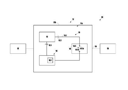
Referring to Figure 1, reference numeral 10 generally indicates an explosives
detonation system in accordance with the invention. The system 10 includes a
detonator 11 having an initiating device 11 a, a shock tube 13, and an
explosive charge
15, with which the detonator 11, and thus the initiating device thereof, is
arranged in a
detonating relationship. The initiating device 11 a is provided inside a
housing lib of
the detonator 11.
The shock tube 13 is arranged in an initiating relationship with the detonator
11, such
arrangement being represented conceptually by connecting line 17. In practice,
the
shock tube 13 will typically be physically connected to the detonator 11, e.g.
by means
of a clamp or, more preferably, by being inserted into an open end of the
detonator 11
or housing thereof with the open end then being crimped about the shock tube,
thereby to provide a seal.
The shock tube 13 is capable of generating and propagating there along a shock
signal by reason of progressive detonation of an explosive substance provided
therein.
In one embodiment of the invention, the shock tube 13 may have a tracing
substance
or tracing chemical included in or mixed with the explosive substance, which
tracing
substance provides, on combustion thereof by reason of combustion of the
explosive
CA 02820862 2013-06-07
WO 2012/077084 PCT/1B2011/055576
18
substance, a detectable chemical compositional property of a product wave of
the
shock signal. This possibility is described in more detail below. The
detectable
chemical compositional property may also be provided by a normal product of
the
explosive substance on combustion or detonation thereof. The explosive
substance
may, in particular, be HMX.
The detonator 11 is an electronic detonator by reason of the nature of its
initiating
device 11a. More particularly, the initiating device 11 a comprises a voltage
source 12
and a fuse head 14, both of which which are located within the detonator
housing lib.
The voltage source 12 and the fuse head 14 form part of a detonation circuit
16
comprising a primary conductive path 16.1, which typically comprises
integrated or
circuitry. In particular, the detonation circuit 16 as well as the fuse head
14, and thus
the electrodes and resistive bridge thereof, may be printed circuitry, having
been
printed onto a substrate. Printing may have been achieved by any one or more
of
inkjet, gravure, screen printing, offset lithography, flexography and other
reel to reel
methods. The electrodes as well as resistive bridge may, in particular, be
printed with
a suitable polymeric or conductive ink, or metallization paste which is gold,
copper,
silver, carbon, stainless steels or aluminum based. When the paste is carbon-
based,
the carbon may particularly be in the form of nanotubes. The energy output
from the
resistive bridge could be enhanced by adding a layer printed in a suitable
chemical
(oxidizer, fuel and or explosive). The substrate may be PET, PEN, PI or coated
paper.
As described hereinafter in more detail, the voltage source 12 may be integral
with the
initiating device 11a, i.e. may be located inside the detonator housing 11 b
and form
part of the initiating device 11 a. It is, however, expected that the voltage
source may
CA 02820862 2013-06-07
WO 2012/077084 PCT/1B2011/055576
19
also be provided separately from the initiating device 11a and/or from the
detonator
11. Thus, the voltage source 12 may be provided inside the detonator housing
11 b,
but not be integral with the initiating device. Further still, the voltage
source may be
provided outside the detonator housing 11b, e.g. being located remotely
therefrom and
then being connected to the detonator 11 and more particularly to the
initiating device
lla by means of respective conducting elements or wires (not shown).
The fuse head 14 comprises two conductive electrodes 14.1a, 14.1b and a
resistive
bridge 14.2 which spans the electrodes. Respective poles 12.1, 12.2 of the
voltage
source 12 are operatively connected to the respective electrodes 14.1a, 14.1b
of the
fuse head 14 along the primary conductive path 16.1. The electrodes 14.1a,
14.1 b
may also be of a printed electronics nature, e.g. being printed by means of
ink jet or
screen printing.
The voltage source 12 is capable of generating a potential difference between
the
conductive electrodes 14.1a, 14.1b which exceeds a breakdown voltage of the
resistive element 14.2. When this occurs, the resistive bridge 14.2 breaks
down and
generates a voltage spark or plasma which, in turn, generates a detonation
signal in
the form of a shock wave which is capable of initiating and, in fact,
detonating or
causing detonation of the explosive charge 15 with which the detonator 11 is
arranged
in a detonating relationship. Of course, in present invention, such initiation
and
detonation can only occur once the initiating device lla has been switched
into the
standby condition in the manner hereinafter described.
CA 02820862 2013-06-07
WO 2012/077084 PCT/1B2011/055576
A switching device 18 is provided in the primary conductive path 16.1, between
one of
the poles 12.1 of the voltage source 12 and one of the conductive electrodes
14.1b of
the fuse head 14.
5 The switching device 18 comprises a transistor 18.1, particularly an
organic thin film
transistor (OTFT). The transistor 18.1 is capable of detecting, when present,
a
switching property a switching signal provided by the shock signal of the
shock tube 13
and of switching the initiating device 11a to the standby condition on
detecting the
switching property. More particularly, the transistor 18.1 is capable of
detecting a
10 chemical compositional component which provides the switching property
of the
switching signal, the transistor 18.1 being sensitive to the chemical
compositional
property as a function of its conductance such that its conductance increases
on
exposure to the switching property. As indicated hereinbefore, the chemical
compositional component may include a tracing chemical, being provided in the
shock
15 tube 13 particularly for providing the chemical compositional component
(as explained
in more detail below) and/or a normal combustion or detonation product of the
shock
tube explosive.
In particular, in order to detect the chemical compositional component, the
transistor
20 18.1 includes a sensing material that is sensitive, in a chemically
reactive sense, to the
chemical compositional component as a function of its conductance, with a
chemical
reaction-activated change in the sensing material on exposure to the switching
compositional component resulting in an increase in the transistor
conductance.
Typically, the sensing material is a conducting polymer, or a conducting
polymer that
CA 02820862 2013-06-07
WO 2012/077084 PCT/1B2011/055576
21
has been treated with or includes a material that may be regarded as the
sensing
material.
In one embodiment of the invention, the chemical compositional component is
carbon
monoxide. In such a case, the sensing material includes polyaniline, tin oxide
(Sn02)
doped with palladium (Pd), complexes of porphyrine, and/or a complex of
phthalocyanine.
In another embodiment of the invention, the chemical composition component,
additionally or alternatively, is or includes hydrogen cyanide (HCN), with the
sensing
material comprising polyaniline or a complex of porphyrine.
In yet another embodiment of the invention, the chemical compositional
component,
alternatively or additionally, is or includes NOR. In such a case, the sensing
material is
selected from or includes polyaniline, poly(3-hexylthiophene), a-
sexithiophene, a
complex of porphyrine, a complex of phthalocyanine, or amorphous
poly(triarylamine).
The capability of the transistor 18.1 to detect the chemical compositional
component
and to switch the initiating device 11 b from the non-detonation initiating
condition to
the standby condition, is by reason of a variable conductance thereof. The
transistor
18.1 therefore has a variable conductance. In the non-detonation initiating
condition,
the conductance of the transistor 18.1 is non-conducive to the conduction of
current
from the voltage source 12 along the conductive path 16.1 to the electrodes
14.1a,
14.1b of the fuse head 14 in order for the detonation initiating voltage to be
generated
across the resistive bridge 14.2. Thus, the transistor 18.1 prevents
generation of the
CA 02820862 2013-06-07
WO 2012/077084 PCT/1B2011/055576
22
detonation initiating voltage difference between the electrodes. In contrast,
in the
standby condition, the conductance of the transistor is conducive to the
conduction of
current from the voltage source 12 along the conductive path 16.1 to the
electrodes
14.1a, 14.1b of the fuse head 14 and thus also to the generation of the
detonation
initiating voltage.
In each of the embodiments of chemical compositional component hereinbefore
mentioned, the sensing material of the transistor 18.1 initially has a
conductance that
is non-conducive to the conduction of current from the voltage source 12 to
the fuse
head 14 in order for the detonation initiating voltage to be generated across
the
resistive bridge 14.2. It will be appreciated that this situation provides the
non-
detonation initiating condition, in that even if the voltage source 12 is
active, the
detonation initiating voltage cannot be generated across the resistive bridge
14.2 and
the resistive bridge 14.2 can thus not be broken down in order to provide the
detonation signal. However, being chemically reactively sensitive to the
respective
chemical compositional components as a function of conductance, exposure of
the
respective sensing materials to the appropriate chemical compositional
component
results in an increase in that material's conductance. Thus, on exposure to
the
switching property, it becomes possible for the voltage source 12 to generate
the
detonation initiating voltage across the resistive bridge 14.2, with the
initiating device
11a thus being switched to the standby condition, in which it awaits an
electrical
detonating signal, in the form of the detonation initiating voltage, in order
to initiate the
explosive charge 15.
CA 02820862 2013-06-07
WO 2012/077084 PCT/1B2011/055576
23
The transistor 18.1 may also, in certain embodiments of the invention, be
capable of
detecting any one or more of pressure, temperature and light. This is
particularly the
case when the switching signal has, in addition to the chemical compositional
component, a pressure component, a temperature component, and a light pulse,
as is
generally the case for shock tube. Each of these may respectively provide a
switching
pressure, a switching temperature, and a switching light pulse, with the
transistor 18.1
then being capable of detecting each of these and, possibly, of switching the
initiating
device 11a to the standby condition, typically in the manner hereinafter
described.
The capability of the transistor 18.1 to detect the switching pressure,
switching
temperature, and switching light pulse, may also be by reason of the variable
conductance thereof, similarly to the capability of the transistor 18.1 to
detect the
chemical compositional component, in the manner hereinbefore described.
When the switching property also comprises a switching pressure, the
transistor 18.1
includes a pressure sensitive material that is sensitive to the switching
pressure as a
function of its conductance, and with a pressure-activated change in the
pressure
sensitive material at the switching pressure resulting in an increase in the
transistor
conductance. The pressure sensitive material can, in particular, include a
pressure
sensitive rubber, in which case it typically constitutes a layer of the
transistor, and a
pressure sensitive laminate, in which case it typically constitutes an
external laminate
of the transistor.
The transistor 18.1 may thus typically comprise an integration of an organic
thin film
transistor (OTFT) with the pressure sensitive material. The pressure sensitive
material
CA 02820862 2013-06-07
WO 2012/077084 PCT/1B2011/055576
24
may, in particular, have a variable resistance that is a function of its
mechanical
deformation, thus imparting a change in conductivity to the OTFT at the
switching
pressure that is sufficient for the conductivity to be conducive to the
generation of the
detonation initiating voltage. One example of such a material is pressure
sensitive
rubber that contains carbon particles and a silicon rubber matrix. Another
example of
a device utilising pressure sensitive rubber for pressure detection is one
based of
space-charge limited transistors (SCLT), having P3HT as an active layer. A
SCLT is a
vertical transistor with a grid electrode inserted between source electrode
and drain
electrode to control the vertical current flow. As pressure is applied to the
pressure
sensitive rubber the resistance and therefore current in the source-drain
circuit is
systematically changed allowing the applied pressure to be monitored.
Another
possibility is the employment of a flexible pressure sensor, possibly through
employment of transparent plastic foil as both the substrate and gate
dielectric of the
transistor 18.1. When the pressure sensitive material comprises a laminate,
the
laminate may typically be a polydimethylsiloxane (PDMS) mold with gold
electrodes. It
is to be noted, however, that OTFT's have an inherent sensitivity to applied
pressure,
for example pentacene transistors having a solution-processed polyvinylphenol
gate
dielectric on a glass substrate.
When the switching property also comprises a switching temperature, thus in
addition
to the chemical compositional component and, possibly, also in addition to the
switching pressure, the transistor includes a temperature sensitive material
that is
sensitive to the switching temperature as a function of its conductance, and
with a
thermally-activated change in the temperature sensitive material at the
switching
temperature resulting in an increase in the transistor conductance. The
temperature
CA 02820862 2013-06-07
WO 2012/077084 PCT/1B2011/055576
sensitive material is typically a polymeric ferroelectric material, preferably
a
polyvinylidene fluoride (PDVF). In such a case the temperature sensitive
material is
present in the transistor as a piezo- or pyroelectric polymer thin film
capacitor that has
thus been integrated with the transistor.
5
When the switching property also comprises a switching light pulse, thus in
addition to
the chemical compositional component and, possibly, also in addition to either
or both
of the switching pressure and the switching temperature, the transistor 18.1
includes a
photoconductive material that is sensitive to the switching light pulse as a
function of
10 its conductance, with a light pulse-activated change in the
photosensitive material at
the switching light pulse resulting in an increase in the transistor
conductance. The
transistor 18.1 may, in particular, include an organic photovoltaic (OPV) cell
that
provides the photoconductive material.
15 Detectors for light pulses usually fall into two broad categories,
namely (i) devices
which integrate together an organic photovoltaic (OPV) cell and an OTFT, using
the
photoresponse of the OPV device to modify the output of the OTFT whilst taking
advantage of the amplification inherent to the transistor, and (ii) devices
which use the
inherent photoconductivity of conducting polymers or blends of conducting
polymers
20 and complimentary electron donor or acceptor molecules in the OTFT. Both
approaches rely on the formation and charge separation of excited states
within the
OTFT upon exposure to incident light. One example of the first type of device
is a
large-area, flexible, and lightweight photo-detectors, also referred to as
sheet-type
image scanners, which are fabricated on plastic film using integrated OTFTs
and
25 organic photodiodes. Another example, is organic photosensors (OPS's)
that are
CA 02820862 2013-06-07
WO 2012/077084 PCT/1B2011/055576
26
integrated a pentacene-based OTFT with a traditional P3HT:PCBM bulk
heterojunction
OPV device. This type of OTFT-based light detector is particularly attractive
in that the
current obtained from the OPV component could conceivably be used to power a
secondary circuit to, for example, time and detonate a primary explosive
charge. It
could also, conceivably, act as voltage source for generating the detonation
initiating
voltage. Furthermore, given the wide range of materials which can be used in
OPV
devices, tailoring to a given spectrum of light (such as from shock tube
emission or a
shock tube light pulse) can be achieved.
Examples of the second type of OTFT optical sensor, those which use the
photoconductivity of conducting polymers, are based thereon that the inherent
photoconductivity of all organic semiconductors implies that all OTFTs based
upon
these materials must show some degree of photoresponse. However, there are
known
to be difficulties associated with the photoresponse of organic
semiconductors, in
particular, inefficient dissociation of the photogenerated excitons into free
carriers and
the long transit times due to poor carrier mobilities. To overcome these
issues the
group there has been proposed an ultra-thin multilayer structure, in which the
photodetector active region consists of 64 alternating layers, varying in
thickness,
ranging from 10 to 160 A for each layer, of, inter alia, Cu phthalocyanine
(CuPc)
(electron donator) and 3,4,9,10-perylenetetracarboxylic bis-benzinnidazole
(PTCBI)
(electron acceptor) grown by ultra-high vacuum organic molecular-beam
deposition.
Low-voltage ambipolar organic phototransistors based on a pentacene/[6,6]-
phenyl-
C61- butyric acid methyl ester (PC61BM) bilayer as the semiconducting layer
with a
self-assembled monolayer as the gate dielectric are also a possibility.
Such
CA 02820862 2013-06-07
WO 2012/077084 PCT/1B2011/055576
27
transistors have been shown to operate below 131 V with electron and hole
mobilities
on the order of 0.1 and 10-3 cm2/Vs, respectively. Importantly, the channel
current of
such transistors are dependent not only on biasing conditions, but also on
intensity of
incident light, allowing the device to be used as an optical sensor. The
external
quantum efficiency and response time of these low-power phototransistors can
be
¨0.8% and 210-225 ms, respectively.
Finally, in regard to light sensitivity, covalently bound organic
donor/acceptor dyads
can be used to enhance charge separation, and thus signal response, in
photoconductive materials for optical detectors. Highly responsive UV-
sensitive field-
effect transistors based on amorphous thin films of such an organic dyad are
known in
literature. Such devices are associated with an optimal responsivity of up to
6.5 NW
for UV light at 370 nm. The underlying mechanism is postulated at the hand of
ultrafast photoinduced intramolecular charge transfers between the acceptor
and the
donor, leading to more facile intermolecular charge transfer. This result
offers a
potential application of organic semiconductors as active materials for UV
detectors.
It is to be noted, importantly, that the switching device 18 can, possibly,
include a
plurality of transistors, each being configured for the detection of a
respective
switching property of the switching signal. Of course, in accordance with the
invention,
the switching device 18 will always include a transistor capable of detecting
the
chemical compositional component. It will be appreciated that, if the
switching device
18 comprises a plurality of transistors, each transistor will, in itself,
provide a
resistance to current that may attempt to pass to the fuse head 14. In order
for such
current to be allowed to pass, it will therefore be necessary, on detection of
each of
CA 02820862 2013-06-07
WO 2012/077084 PCT/1B2011/055576
28
their respective switching properties, for the conductance of each transistor
to increase
sufficiently for the detonation initiating voltage to be generated across the
resistive
bridge 14.2. Thus, for the standby condition to be assumed by the initiating
device
11 a in such a case, it is necessary for all of the switching properties
associated with
the respective transistors to be present in the switching signal. It will be
appreciated
that such a situation therefore provides for multiple detection modes being
required
from the switching device 18.
In a particular embodiment of the invention, and as alluded to hereinabove,
the voltage
source 12 may be an integrated voltage source, being integrated with the
primary
conductive path 16.1.
The voltage source 12 may also, in particular, be in the form of a chargeable
or
rechargeable voltage source. In such a case, the voltage source 12 may
comprise or
be operatively associated with a charging component that is capable, on
exposure to
the switching property, of charging the voltage source 12 and thus rendering
it
dischargeable when the initiating device 11 a is in the standby condition,
thereby to
apply the detonation initiating voltage across the resistive bridge 14.2.
Such a charging component may typically be or include a photosensitive cell,
such as
an organic photovoltaic cell, or other photo-responsive component, such as a
transistor.
Alternatively, the charging component itself may be the voltage source 12.
Thus, in
accordance with the invention, the charging component may also form or form
part of
CA 02820862 2013-06-07
WO 2012/077084 PCT/1B2011/055576
29
the voltage source 12, particularly when the voltage source 12 is a battery
that is
chargeable or rechargeable, e.g. including a photosensitive material, possible
forming
part of a photovoltaic cell that is included in the battery.
Thus, electrical energy built up in the voltage source 12 on exposure to the
switching
property is then released once the conductance of the transistor 18.1 is of a
sufficient
magnitude for the detonation initiating voltage to be generated across the
resistive
bridge 14.2 by the, now charged, voltage source 12, i.e. in the standby
condition. It
will be appreciated that through discharge of the charged voltage source, the
initiating
device 11a thus becomes switched from the standby condition into the
detonation
initiating condition.
The charging component may be charged by any one or more of the switching
properties described hereinbefore and not necessarily only by the chemical
compositional component. Preferably, the charging component is capable of
being
charged and thus of charging the voltage source by a switching property that
moves
faster than the other switching properties, e.g. light. Thus, the charging
component
may charge the voltage source 12 prior to switching of the initiating device
lla into the
standby condition. The charging component may therefore typically be a
photosensitive transistor, a photodiode or other photosensitive device. In
such a case,
the shock tube 13 may, in particular, include a photo-luminescent additive
that
enhances, extends or increases the light energy output of an explosive
substance
carried inside the shock tube 13. Such a photo-luminescent additive may
include either
or both of fluorescent and/or phosphorescent organic or inorganic materials
that
increase or modify the wavelength of the emitted light pulse or otherwise
alter the
CA 02820862 2013-06-07
WO 2012/077084 PCT/1B2011/055576
optical emission properties of the shock tube 13 so as to enhance the light
(energy)
that is emitted from the shock tube 13 for photovoltaic applications.
It is expected that such a configuration of the present invention is
particularly
5 advantageous in that the voltage source 12 is, in effect, powered by the
same shock
signal that switches the initiating device 11a into the standby condition.
Initiating of the
explosive can then be rendered fully dependent on a shock signal having very
specific
switching properties.
10 It is to be appreciated that application of the detonation initiating
voltage would not
necessarily lead immediately to detonation of the explosive charge. In this
regard, the
initiating device 11a may have incorporated therein timing and delay
components that
are powered by application of the detonation initiating voltage and then, in
turn, cause
detonation of the explosive.
In use, the transistor 18.1 of the switching device 18 will initially, i.e. at
manufacture
most likely, have a conductance of magnitude insufficient for conducting
sufficient
current from the voltage source 12, of predetermined load, for the voltage
source 12 to
generate the detonation initiating voltage across the resistive bridge 14.2.
The
initiating device 11a is thus initially in the non-detonation initiating
condition. The
transistor 18.1 will, however, be configured in the manner hereinbefore
described and
thus be capable of detecting, as a function of its conductance, a switching
property of
a switching signal transmitted by the shock tube 13, such a switching property
being at
least a chemical compositional component of the switching signal and,
optionally, also
any one or more of a switching pressure, a switching temperature and a
switching light
CA 02820862 2013-06-07
WO 2012/077084 PCT/1B2011/055576
31
pulse. The detonator 11, with the initiating device 11 a and the transistor
18.1, is then
positioned in a detonating relationship relative to the explosive charge 15.
The shock
tube 13, being capable of transmitting a shock signal having a product wave
including
the chemical compositional component and, if applicable, the switching
pressure, the
switching temperature and the switching light pulse, is then connected to, or
at least
provided in an initiating relationship relative to, the detonator 11.
Once detonation of the explosive charge 15 is to occur, the shock tube 13 is
initiated
remotely from the detonator 11, with the shock signal then being propagated
there
along. Once the shock signal is in proximity to the initiating device 11a,
sufficiently so
that the switching property / properties thereof are detected by the
transistor/s 18.1,
the conductance of the transistor/s 18.1 thus increases sufficiently to allow
for the
detonation initiating voltage to be generated by the voltage source 12 across
the
resistive bridge 14.2, with the initiating device 11a thus being switched to
the standby
condition. With the conductance of the transistor/s 18.1 having thus
increased, the
initiating device 11a has become susceptible to receiving and conducting,
along the
primary conductive path 16.1, sufficient current from the voltage source 12
for the
*detonation initiating voltage to be generated by the voltage source 12 across
the
resistive bridge 14.2. Activation of the voltage source 12 therefore switches
the
initiating device 11a to the detonation initiating condition in which the
detonation
initiating voltage is applied across the resistive bridge 14.2, which results
in breakdown
of the resistive bridge 14.2 and generation a spark or plasma, emitting a
detonation
initiating shock wave that initiates the explosive charge 15.
CA 02820862 2013-06-07
WO 2012/077084 PCT/1B2011/055576
32
In a particular embodiment of the invention, the shock tube 13 may be a shock
tube in
accordance with the invention, having a hollow, elongate body, inside which a
shock
tube explosive is contained. The shock tube explosive is, in particular, HMX,
as also
indicated above. The shock signal hereinbefore referred to is thus provided by
progressive detonation of the HMX. Other explosive substances, associated with
shock tube, can, of course, also be employed as shock tube explosive.
As indicated above, the shock tube 13 also, preferably, includes a tracer
chemical and,
optionally, a photo-luminescent chemical.
The tracer chemical is, in particular, a chemical that is not, or on
combustion,
detonation or decomposition does not provide, a chemical that is the same as a
detonation or combustion product of the shock tube explosive.
When present in the shock tube 13, the tracer chemical provides the chemical
compositional component, either in itself or by way of combustion, detonation
or
decomposition product thereof. The presence of the tracer chemical is, in such
a
case, therefore a prerequisite for the initiating device to be switched from
the non-
detonation initiating condition into the standby condition.
In a particular embodiment of the invention, the tracer chemical is a gas-
generating
chemical.
CA 02820862 2013-06-07
WO 2012/077084 PCT/1B2011/055576
33
The photo-luminescent chemical may particularly include a fluorescent and/or a
phosphorescent chemical or a precursor for such a chemical or for another
luminescent chemical.
The photo-luminescent chemical serves, in use, particularly to enhance,
amplify and/or
adjust, i.e. impart particular properties of wavelength and/or intensity to,
the light pulse
component of the shock signal of the shock tube. The photo-luminescent
chemical
may therefore be selected particularly for compatibility with a particular
photosensitive
material of the transistor 18.1 and/or of the chargeable component of the
voltage
source 12. In the case of the voltage source 12, the photo-luminescent
chemical is
preferably selected for generating a photo-response from the voltage source 12
that is
sufficient for the voltage source 12 to generate the detonation initiating
voltage
difference across the electrodes 14.1a, 14.1b.
The photo-luminescent chemical may in particular, be inorganic and may
comprise a
rare earth metal salt or combinations of two or more such salts. Typically,
the salts
may be selected from oxide salts, nitrate salts, perchlorate salts,
persulphate salts and
combinations thereof. Alternatively, of course, the photo-luminescent chemical
may
be a precursor for such a salt or another luminescent oxide.
The present invention therefore envisages a detonation system, such as the
detonation system 10, that is capable of being switched from a non-detonation
initiating condition, in which it cannot operatively accept a detonation
initiating signal,
to a standby condition, in which it can operatively accept the detonation
initiating
signal, with such switching being effected by means of a switching device that
CA 02820862 2013-06-07
WO 2012/077084 PCT/1B2011/055576
34
comprises a transistor which is capable switching the initiating device from
the non-
detonation initiating condition to the standby condition on detection of at
least a
chemical compositional component of a switching signal that comprises a shock
signal
transmitted by shock tube.
The Applicant believes that an approach to detonator system operation as is
described
herein, i.e. by rendering an initiating device susceptible to initiation only
under
predetermined conditions, will be particularly beneficial to operational
safety of such
detonator systems, as inadvertent detonation caused by premature detonation
initiating signal transmission will be prevented. The present invention
therefore
requires operation of a detonator system to proceed along a particular chain
of events
in order for detonation to result.
In particular, the Applicant believes that the employment of multiple
detection modes,
including at least a detection mode for a chemical compositional component of
the
switching or shock signal, in a switching device employed in a detonator
system
according to the invention renders a particular improvement in the operational
safety of
detonator systems. This is by reason thereof that, whereas signal components
of
pressure, temperature and light are not readily susceptible to accurate
control for the
purposes of providing narrow predetermined signals, chemical composition can,
to a
certain extent at least, be controlled, e.g. by including a particular
compositional
component in the explosive contained by the shock tube with which the system
is to be
employed.
CA 02820862 2013-06-07
WO 2012/077084 PCT/1B2011/055576
The important feature of the present invention of chemical compositional
component
detection is therefore regarded as imparting particular advantages of improved
control
and safety to the present invention.
5 Additionally, the present invention envisages an enhanced shock tube that
contains, in
addition to a shock tube explosive thereof, a tracer chemical and, optionally,
a photo-
luminescent chemical. It is believed by the Applicant that such additives will
aid in
expanding the functionality of shock tube to more limited compatibility with
detonators
tailored therefor and also render the shock tube useful in managing safety of
explosive
10 and detonator systems, such as the system of the present invention.