Note: Descriptions are shown in the official language in which they were submitted.
CA 02821617 2013-06-13
WO 2012/084655
PCT/EP2011/072818
MICROWAVE PLASMA REACTORS AND SUBSTRATES
FOR SYNTHETIC DIAMOND MANUFACTURE
Field of Invention
The present invention relates to a microwave plasma reactor for manufacturing
synthetic diamond material using chemical vapour deposition techniques.
Certain
embodiments relate to substrates for use in a microwave plasma reactor for
synthetic
diamond manufacture.
Background of Invention
Chemical vapour deposition (CVD) processes for synthesis of diamond material
are
now well known in the art. Useful background information relating to the
chemical
vapour deposition of diamond materials may be found in a special issue of the
Journal
of Physics: Condensed Matter, Vol. 21, No. 36 (2009) which is dedicated to
diamond
related technology. For example, the review article by R. S Balmer et al.
gives a
comprehensive overview of CVD diamond materials, technology and applications
(see "Chemical vapour deposition synthetic diamond: materials, technology and
applications" J. Phys.: Condensed Matter, Vol. 21, No. 36 (2009) 364221).
Being in the region where diamond is metastable compared to graphite,
synthesis of
diamond under CVD conditions is driven by surface kinetics and not bulk
thermodynamics. Diamond synthesis by CVD is normally performed using a small
fraction of carbon (typically (5%), typically in the form of methane although
other
carbon containing gases may be utilized, in an excess of molecular hydrogen.
If
molecular hydrogen is heated to temperatures in excess of 2000 K, there is a
significant dissociation to atomic hydrogen. In the presence of a suitable
substrate
material, diamond can be deposited.
Atomic hydrogen is essential to the process because it selectively etches off
non-
diamond carbon from the substrate such that diamond growth can occur. Various
methods are available for heating carbon containing gas species and molecular
hydrogen in order to generate the reactive carbon containing radicals and
atomic
CA 02821617 2013-06-13
WO 2012/084655
PCT/EP2011/072818
hydrogen required for CVD diamond growth including arc-jet, hot filament, DC
arc,
oxy-acetylene flame, and microwave plasma.
Methods that involve electrodes, such as DC arc plasmas, can have
disadvantages due
to electrode erosion and incorporation of material into the diamond.
Combustion
methods avoid the electrode erosion problem but are reliant on relatively
expensive
feed gases that must be purified to levels consistent with high quality
diamond
growth. Also the temperature of the flame, even when combusting oxy-acetylene
mixes, is insufficient to achieve a substantial fraction of atomic hydrogen in
the gas
stream and the methods rely on concentrating the flux of gas in a localized
area to
achieve reasonable growth rates. Perhaps the principal reason why combustion
is not
widely used for bulk diamond growth is the cost in terms of kWh of energy that
can
be extracted. Compared to electricity, high purity acetylene and oxygen are an
expensive way to generate heat. Hot filament reactors while appearing
superficially
simple have the disadvantage of being restricted to use at lower gas pressures
which
are required to ensure relatively effective transport of their limited
quantities of
atomic hydrogen to a growth surface.
In light of the above, it has been found that microwave plasma is the most
effective
method for driving CVD diamond deposition in terms of the combination of power
efficiency, growth rate, growth area, and purity of product which is
obtainable.
A microwave plasma activated CVD diamond synthesis system typically comprises
a
plasma reactor vessel coupled both to a supply of source gases and to a
microwave
power source. The plasma reactor vessel is configured to form a resonance
cavity
supporting a standing microwave. Source gases including a carbon source and
molecular hydrogen are fed into the plasma reactor vessel and can be activated
by the
standing microwave to form a plasma in high field regions. If a suitable
substrate is
provided in close proximity to the plasma, reactive carbon containing radicals
can
diffuse from the plasma to the substrate and be deposited thereon. Atomic
hydrogen
can also diffuse from the plasma to the substrate and selectively etch off non-
diamond
carbon from the substrate such that diamond growth can occur.
2
CA 02821617 2013-06-13
WO 2012/084655
PCT/EP2011/072818
A range of possible microwave plasma reactors for diamond film growth via a
chemical vapour deposition (CVD) process are known in the art. Such reactors
have a
variety of different designs. Common features include: a plasma chamber; a
substrate
holder disposed in the plasma chamber; a microwave generator for forming the
plasma; a coupling configuration for feeding microwaves from the microwave
generator into the plasma chamber; a gas flow system for feeding process gases
into
the plasma chamber and removing them therefrom; and a temperature control
system
for controlling the temperature of a substrate on the substrate holder.
The present inventors consider that when designing a microwave plasma reactor
process for diamond film growth, to achieve a successful industrial process
requires
the assessment of a number of considerations including: chamber and microwave
power coupling configuration; gas flow characteristics; and substrate design
and
temperature control. Certain embodiments of the present invention are
primarily
concerned with the aspects of substrate design and temperature control.
The most commonly used substrate for CVD diamond growth is silicon. One
problem
with using silicon as a substrate for CVD diamond growth in a microwave plasma
growth process is power absorption by the silicon at high temperatures,
leading to
thermal runaway and fracture. Another problem is that silicon is readily
incorporated
into CVD diamond during growth, being particularly visible as the 737nm Si-V
defect. As such, the use of a silicon substrate can detrimentally affect the
purity of the
CVD diamond product. Yet another problem is that after growth of a CVD diamond
wafer on a silicon substrate, recovery of the CVD diamond wafer may require,
for
example, one of mechanical or acid removal. These additional processing steps
increase the time and expense of an industrially implemented process.
In light of the above, it is evident that it would be desirable to find an
alternative
substrate material which solves these problems.
One possibility for a substrate material is a carbide forming refractory metal
such as
tungsten, molybdenum, niobium, or alloys thereof Such substrates have already
been
proposed in the art. For example, U55261959 suggests a refractory metal
substrate
material such as molybdenum in the form of a planar circular disk.
Alternatively,
3
CA 02821617 2013-06-13
WO 2012/084655
PCT/EP2011/072818
Whitfield et al. suggest the use of a tungsten substrate (see "Nucleation and
growth of
diamond films on single crystal and polycrystalline tungsten substrates",
Diamond
and Related Materials, Volume 9, Issues 3-6, April-May 2000, Pages 262-268).
Specifically, Whitfield et al. disclose the use of a polycrystalline tungsten
disc 6.3
mm thick and 50 mm in diameter and a single crystal tungsten disc 6.3 mm thick
and
8 mm in diameter in a 2.45 GHz microwave plasma reactor. The substrates were
subjected to preparation steps including polishing to a mirror finish with a 1-
3
micrometer diamond abrasive and cleaning via ultrasonic washing and an in situ
plasma etch. Substrate temperatures were monitored using optical pyrometry and
an
embedded thermocouple during CVD diamond growth. Spontaneous delamination of
the CVD diamond wafer from the tungsten substrate on cooling after growth is
also
disclosed to yield a free-standing diamond wafer due to the differences in
thermal
expansion coefficient between the CVD diamond wafer and the tungsten
substrate.
Whitfield et al. note that generally in their experiments the substrates were
not reused
but in the few cases where re-use did occur, substrates were lapped and
polished for at
least 24 hours to remove the thin carbide layer formed during the previous
growth
run.
In light of the above, it is evident that carbide forming refractory metals
may provide
an attractive alternative to silicon substrates. Despite this, the present
inventors have
experienced a number of problems when using such substrates. These include:
non-
uniform CVD diamond growth over the substrate; delamination of the CVD diamond
wafer from the substrate during CVD diamond growth; and crack initiation and
propagation during cooling after growth of the CVD diamond wafer. These
problems
tend to be exacerbated when larger substrates are used for growing large area
polycrystalline diamond discs (e.g. 80 mm diameter or more) or when growing a
plurality of single crystal diamonds in a single growth run on a plurality of
single
crystal diamond substrates adhered to a refractory metal substrate over a
relatively
large area (e.g. 80 mm diameter or more). This is particularly problematic as
there is
an on going need to increase the area over which high quality, uniform CVD
diamond
can be grown. Furthermore, these problems tend to be exacerbated when the
substrates are reused in subsequent growth runs. This is particularly
problematic as
the substrates are expensive and reuse is desirable in an economically
competitive
industrial process.
4
CA 02821617 2013 06 13
WO 2012/084655
PCT/EP2011/072818
It is an aim of certain embodiments of the present invention to at least
partially
address one or more of these problems. In particular, it is an aim of certain
embodiments of the present invention to provide more uniform and/or more
consistent
CVD diamond products.
Summary of Invention
According to a first aspect of the present invention there is provided a
microwave
plasma reactor for manufacturing synthetic diamond material via chemical
vapour
deposition, the microwave plasma reactor comprising:
a microwave generator configured to generate microwaves at a frequency f;
a plasma chamber comprising a base, a top plate, and a side wall extending
from said base to said top plate defining a resonance cavity for supporting a
microwave resonance mode between the base and the top plate;
a microwave coupling configuration for feeding microwaves from the
microwave generator into the plasma chamber;
a gas flow system for feeding process gases into the plasma chamber and
removing them therefrom;
a substrate holder disposed in the plasma chamber and comprising a
supporting surface for supporting a substrate; and
a substrate disposed on the supporting surface, the substrate having a growth
surface on which the synthetic diamond material is to be deposited in use,
wherein the substrate dimensions and location within the resonance cavity are
selected to generate a localized axisymmetric Ez electric field profile across
the
growth surface in use, the localized axisymmetric Ez electric field profile
comprising
a substantially flat central portion bound by a ring of higher electric field,
the
substantially flat central portion extending over at least 60% of an area of
the growth
surface of the substrate and having an Ez electric field variation of no more
than 10%
of a central Ez electric field strength, the ring of higher electric field
being disposed
around the central portion and having a peak Ez electric field strength in a
range 10%
to 50% higher than the central Ez electric field strength.
CA 02821617 2013-06-13
WO 2012/084655
PCT/EP2011/072818
According to an alternative definition of the first aspect of the present
invention there
is provided a microwave plasma reactor for manufacturing synthetic diamond
material
via chemical vapour deposition, the microwave plasma reactor comprising:
a microwave generator configured to generate microwaves at a frequency f;
a plasma chamber comprising a base, a top plate, and a side wall extending
from said base to said top plate defining a resonance cavity for supporting a
microwave resonance mode between the base and the top plate;
a microwave coupling configuration for feeding microwaves from the
microwave generator into the plasma chamber;
a gas flow system for feeding process gases into the plasma chamber and
removing them therefrom;
a substrate holder disposed in the plasma chamber and comprising a
supporting surface for supporting a substrate; and
a substrate disposed on the supporting surface, the substrate having a growth
surface on which the synthetic diamond material is to be deposited in use,
wherein a ratio of substrate diameter / height of the growth surface of the
substrate is in a range 10 to 14, 11 to 13.5, or 11.0 to 12.5, wherein the
height of the
growth surface of the substrate is relative to a mean height of a surface
surrounding
the substrate.
According to a second aspect of the present invention there is provided a
substrate for
use in a microwave plasma reactor according to the first aspect of the
invention, the
substrate comprising:
a cylindrical disc of a carbide forming refractory metal having a flat growth
surface on which CVD diamond is to be grown and a flat supporting surface
opposed
to said growth surface,
wherein the cylindrical disc has a diameter of 80 mm or more,
wherein the growth surface has a flatness variation no more than 100 um, and
wherein the supporting surface has a flatness variation no more than 100 um.
According to a third aspect of the present invention there is provided a
method of
manufacturing synthetic diamond material using a chemical vapour deposition
process, the method comprising:
6
CA 02821617 2013 06 13
WO 2012/084655
PCT/EP2011/072818
providing a reactor configured for manufacturing synthetic diamond material;
locating a substrate on a substrate holder within the reactor, the substrate
comprising a growth surface on which synthetic diamond material is to be
grown;
feeding process gases into the reactor; and
growing synthetic diamond material on the growth surface of the substrate,
wherein the method further comprises:
taking at least two temperature measurements, including one or more
measurements in a central region of the growth surface of the substrate and
one or
more measurements in a peripheral region of the growth surface of the
substrate
during growth of the synthetic diamond material; and
controlling a temperature difference between the central region and the
peripheral region of the growth surface of the substrate during growth of the
synthetic
diamond material based on the at least two temperature measurements,
wherein the temperature of the growth surface of the substrate during growth
of the synthetic diamond material is controlled to fulfil the condition 5 C <
Tc ¨ Te<
120 C, where Tc is a temperature in the central region of the growth surface
of the
substrate and Te is a temperature in the peripheral region of the growth
surface of the
sub strate.
According to a fourth aspect of the present invention there is provided a
method of
manufacturing synthetic diamond material using a chemical vapour deposition
process, the method comprising:
providing a reactor configured for manufacturing synthetic diamond material;
locating a substrate over a substrate holder within the reactor, the substrate
comprising a growth surface on which synthetic diamond material is to be
grown;
feeding process gases into the reactor; and
growing synthetic diamond material on the growth surface of the substrate,
wherein the synthetic diamond material is grown to form a polycrystalline
diamond wafer having a diameter of at least 120 mm,
and wherein the polycrystalline diamond wafer is spontaneously delaminated
from the substrate on cooling after the chemical vapour deposition process is
completed to yield a free-standing polycrystalline diamond wafer which is
substantially crack free over at least a central region thereof, wherein the
central
region is at least 70% of a total area of the free-standing polycrystalline
diamond
7
CA 02821617 2013 06 13
WO 2012/084655
PCT/EP2011/072818
wafer, and wherein the central region has no cracks which intersect both
external
major faces of the free-standing polycrystalline diamond wafer and extend
greater
than 2 mm in length.
Brief Description of the Drawings
For a better understanding of the present invention and to show how the same
may be
carried into effect, embodiments of the present invention will now be
described by
way of example only with reference to the accompanying drawings, in which:
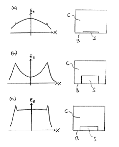
Figures 1(a) to 1(c) show electric field profile plots for varying heights of
substrate
within a microwave plasma reactor;
Figures 2(a) to 2(c) show how the height of the growth surface of the
substrate is
calculated relative to relative to a mean height of a surface surrounding the
substrate;
Figure 3 shows a cross-sectional view of a microwave plasma reactor configured
according to an embodiment of the present invention;
Figure 4 shows a plan view of a portion of the microwave plasma reactor in
more
detail illustrating a substrate holder and spacer wires;
Figure 5 shows a cross-sectional view of another microwave plasma reactor
configured to include a temperature modifying ring disposed over the substrate
holder
and around the substrate;
Figure 6 shows the temperature modifying ring in more detail;
Figure 7 shows a substrate according to an embodiment of the present
invention; and
Figures 8(a) to 8(d) show various possible alternative substrate
configurations.
Detailed Description of Certain Embodiments
8
CA 02821617 2013-06-13
WO 2012/084655
PCT/EP2011/072818
It is considered desirable to provide a microwave plasma reactor which is
configured
to form a uniform, large area plasma above a substrate in order to provide
uniform
CVD diamond growth over a large area of the substrate. Intuitively, one would
expect that a microwave plasma reactor should be configured to support a
uniform
electric field above the substrate in order to form such a uniform plasma. The
first
aspect of the present invention is based on the seemingly counter-intuitive
finding that
a non-uniform electric field of a particular form can produce a more uniform
plasma
over a larger area than a corresponding uniform underlying electric field and
that this
can lead to more uniform CVD diamond growth over larger areas. In particular,
the
present inventors have found that it is preferable to form an electric field
having an
axisymmetric Ez profile comprising a substantially flat central portion bound
by a ring
of higher electric field, the substantially flat central portion extending
over at least
60% of an area of the growth surface of the substrate and having an Ez
electric field
variation of no more than 10%, 8%, 6%, 5%, 4%, 3%, 2%, or 1% of a central Ez
electric field strength. The ring of higher electric field is disposed around
the central
portion and has a peak Ez electric field strength in a range 10% to 50%, 10%
to 40%,
15% to 30%, or 15% to 25% higher than the central Ez electric field strength.
It has
been found that the ring of higher electric field can aid in pulling the
plasma outwards
to form a flat, large area plasma above the substrate. Furthermore, as the
plasma
edges have higher radiative and convective losses, the ring of higher electric
field is
considered advantageous to compensate for such losses. The uniform plasma may
then provide uniform heat flow towards the underlying substrate and uniform
transport of active species to the growth surface of the substrate to yield
uniform CVD
diamond growth over large areas.
It has been found that an electric field profile as previously described can
be formed
by selecting suitable substrate dimensions and positioning the substrate in
the correct
location within the resonance cavity of the plasma reactor. In this regard, it
is
possible to model the electric field for particular chamber configurations to
determine
the electric field profile above the substrate growth surface. The electric
field profile
may be modelled by performing electromagnetic field calculations for a
resonance
cavity of specified dimensions at resonance (not necessarily at driving
frequency).
The calculations can be made using an Eigenvalue differential equation solver.
The
localized axisymmetric Ez electric field profile can vary according to the
height at
9
CA 02821617 2013-06-13
WO 2012/084655
PCT/EP2011/072818
which it is calculated relative to the growth surface of the substrate. In
accordance
with embodiments of the present invention the localized axisymmetric Ez
electric field
profile is calculated at a height above the growth surface of the substrate
of: 4 mm, 6
mm, or 8 mm for a microwave frequency f in a range 400 MHz to 500 MHz; 2 mm, 3
mm, or 4 mm for a microwave frequency fin a range 800 MHz to 1000 MHz; or 0.7
mm, 1.0 mm, or 1.5 mm for a microwave frequency f in a range 2300 MHz to 2600
MHz.
It has been found that the electric field profile is significantly perturbed
when a
substrate is introduced into the resonance cavity as can be shown by modelling
or
empirical measurement. In this regard, Figures 1(a) to 1(c) illustrate
electric field
profile plots showing how the electric field varies with differing height of a
substrate
within a resonance cavity of a plasma reactor. The plots show the magnitude of
the
electric field Ez on the Y-axis against the lateral position X across the
diameter of the
resonance cavity above the substrate.
Figure 1(a) illustrates the electric field profile when the growth surface of
the
substrate S is located just above a base B of the resonance cavity C. The
electric field
profile is dominated by that of the empty chamber which is a Jo Bessel
function for a
TMoin chamber. There is only a slight contribution to the electric field
magnitude
from the upper edge of the substrate forming a coaxial mode set up between the
substrate and the chamber wall. In this arrangement, the electric field is
high above a
central region of the substrate and drops off significantly towards the edge
of the
substrate. As such, this electric field profile results in poor CVD diamond
growth in a
peripheral region of the substrate growth surface.
Figure 1(b) illustrates the electric field profile when the growth surface of
the
substrate S is located high above the base B of the resonance cavity C. The
electric
field profile is now dominated by the coaxial mode set up between the
substrate and
the chamber wall which decays evanescently into a central region of the
chamber. In
this arrangement, the electric field is high above a peripheral region of the
substrate
and drops off towards the central region of the substrate. As such, this
electric field
profile results in poor CVD diamond growth in a central region of the
substrate
growth surface.
CA 02821617 2013-06-13
WO 2012/084655
PCT/EP2011/072818
Figure 1(c) illustrates the electric field profile when the growth surface of
the
substrate S is located at the correct height above a surrounding surface
within the
resonance cavity C. The electric field profile of the empty chamber is
balanced with
the coaxial mode set up between the substrate and the chamber wall to form a
substantially uniform electric field region over the majority of the substrate
with a
ring of higher electric field localized around the substrate edge. The central
region of
the electric field is substantially uniform but has a slightly lower electric
field region
just inside the ring of higher electric field localized around the substrate
edge. One
would think that this lower electric field region would lead to poor CVD
diamond
growth at this region of the growth surface. However, in practice it has been
found
that the higher electric field ring immediately outside the region of lower
electric field
aids in pulling the plasma outwards, compensating for the slight non-
uniformity in the
central region and resulting in a large, flat, uniform plasma over the
majority of the
substrate enabling uniform CVD diamond growth over large areas.
It should be noted that while the electric field profile is a property present
when the
microwave plasma reactor in use, it is also uniquely defined when not in use
by
modelling the microwave plasma reactor's electric field profile either at its
resonant
frequencies, or when modelled as being present if driven by a given frequency.
Either
of these models may be applied to a microwave plasma reactor to determine its
electric field profile without undue burden.
While the first aspect of the present invention has been described above in
relation to
the electric field profile, which requires modelling (e.g. modelled at
resonance) or
empirical measurement to determine, a more simplistic definition may be given
in
terms of simple dimensional data for the substrate and its location within the
resonance cavity of a plasma reactor. In practice, the present inventors have
found
that a large, flat, uniform plasma over the majority of the substrate enabling
uniform
CVD diamond growth over large areas can be achieved when a ratio of substrate
diameter / height of the growth surface of the substrate is in a range 10 to
14, 11 to
13.5, or 11.0 to 12.5, wherein the height of the growth surface of the
substrate is
relative to a mean height of a surface surrounding the substrate. Accordingly,
this
alternative definition of the first aspect of the invention may be utilized
without
11
CA 02821617 2013-06-13
WO 2012/084655
PCT/EP2011/072818
modelling or empirical measurement. However, if an arrangement falls outside
these
ranges, it is envisaged that utilizing some alternative chamber geometry it
may still be
possible to form the electric field profile as previously described. In this
case,
modelling or empirical measurements may be required in order to confirm
whether or
not the arrangement conforms with the first aspect of this invention.
Conversely, if an
arrangement falls outside the definition of the first aspect of the invention
based on
the electric field profile it may still fall within the alternative definition
based on the
ratio of substrate diameter / height of the growth surface of the substrate.
This may be
the case if the dimensions and location of the substrate within the plasma
chamber are
selected to form an electric field profile as described but some further
element or
elements are provided to alter the electric field profile above the substrate.
For
example, as described later a metallic ring may be located around the
substrate to
reduce the magnitude of the high electric field ring located above the edge of
the
substrate. Alternatively, or additionally, the substrate holder may be
profiled to
perturb the electric field in order to reduce the magnitude of the high
electric field
ring located above the edge of the substrate. Other electric field modifying
elements
are also envisaged. For example, further metallic bodies which perturb the
electric
field profile may be located on the substrate holder such as metallic inserts
located
under the substrate. As such, these arrangements may be configured to have the
correct substrate diameter/growth surface height ratio while having an
electric field
profile without a significant high electric field ring located above the edge
of the
sub strate.
For an arrangement in which the substrate holder is the same diameter as the
substrate, the substrate holder will be located wholly under the substrate and
the
surface surrounding the substrate may be formed by the base of the plasma
chamber.
As such, in this case the mean height of the surface surrounding the substrate
will
equate to the height of the base B of the plasma chamber C and the height of
the
growth surface of the substrate, Hgs, will be measured from the base of the
plasma
chamber surrounding the substrate S and substrate holder SH as illustrated in
Figure
2(a). Alternatively, for an arrangement in which the substrate holder is much
larger
than the substrate thus forming a large flat surface which surrounds the
substrate, the
mean height of the surface surrounding the substrate will equate to a top
surface of the
substrate holder. As such, in this case the height of the growth surface of
the
12
CA 02821617 2013-06-13
WO 2012/084655
PCT/EP2011/072818
substrate, Hgs, will be measured from the top surface of the substrate holder
SH
surrounding the substrate S as illustrated in Figure 2(b). For an arrangement
in which
the substrate holder extends outwards from the substrate with a sloped,
curved, or
stepped top surface surrounding the substrate then the mean height of the
local
surrounding surface, Hiss, can be defined by a mean of a height, Thocaz, of a
cross
section between the edge of the substrate, at Rs, and a distance approximately
two
times the thickness of the substrate, 2x Ts, away from the substrate edge,
taken in a
radial direction, X:
Rs+2Ts
1
HIss =¨ SHlocaldX
2Rs Rs
Such an arrangement is illustrated in Figure 2(c) for a sloped substrate
holder. For
example, for a substrate holder having a top surface sloping away from the
substrate
at an angle of 45 to a distance 2x Ts from the substrate in a radial
direction, the mean
height of the surface surrounding the substrate will equate to half the height
of the
substrate holder SH. As such, in this case the height of the growth surface of
the
substrate, Hgs, will be measured from half the height of the substrate holder
SH.
In relation to the above, it has been found that providing a step of a
particular height
between the substrate growth surface and the local surrounding surface
perturbs the
electric field profile of the plasma chamber in such a way that the electric
field profile
of the empty chamber is balanced with a coaxial mode set up between the
substrate
and the chamber wall to form a substantially uniform electric field region
over the
majority of the substrate with a ring of higher electric field localized
around the
substrate edge as previously described.
Embodiments of the present invention are particularly suited for application
in TMoin
resonance chambers. The particular geometry required to implement the first
aspect
of the invention will also depend on the operational frequency of the plasma
reactor.
Examples of suitable geometries are set out below.
13
CA 02821617 2013-06-13
WO 2012/084655
PCT/EP2011/072818
The substrate diameter may be selected to be in the range: 165 mm to 415 mm,
185
mm to 375 mm, 205 mm to 375 mm, 205 mm to 330 mm, or 240 mm to 330 mm for a
microwave frequency f in the range 400 to 500 MHz; 80 mm to 200 mm, 90 mm to
180 mm, 100 mm to 180 mm, 100 mm to 160, or 115 mm to 160 mm for a microwave
frequency fin the range 800 to 1000 MHz; or 30 mm to 75 mm, 33 mm to 65 mm, 37
mm to 65 mm, 37 mm to 58 mm, or 42 mm to 58 mm for a microwave frequency f in
the range 2300 to 2600 MHz.
The height of the growth surface of the substrate above the mean height of the
surrounding surface may be selected to be in the range: 10 mm to 30 mm or 14
mm to
27 mm for a microwave frequency fin the range 400 to 500 MHz; 5 mm to 15 mm or
7 mm to 13 mm for a microwave frequency f in the range 800 to 1000 MHz; or 2.0
mm to 5.5 mm or 2.5 mm to 5.0 mm for a microwave frequency fin the range 2300
to
2600 MHz.
Particularly useful height and diameter combinations for a number of
operational
frequency bands are given below.
If the microwave frequency f is in the range 400 MHz to 500 MHz, the substrate
diameter and the height of the growth surface of the substrate above the mean
height
of the surrounding surface within the resonance cavity may be optionally
selected
such that:
if the substrate diameter is in the range 180 mm to 230 mm, the height of the
growth surface is in the range 14 mm to 20 mm;
if the substrate diameter is in the range 230 mm to 270 mm, the height of the
growth surface is in the range 20 mm to 24 mm; or
if the substrate diameter is in the range 270 mm to 310 mm, the height of the
growth surface is in the range 22 mm to 27 mm.
If the microwave frequency f is in the range 800 MHz to 1000 MHz, the
substrate
diameter and the height of the growth surface of the substrate above the mean
height
of the surrounding surface within the resonance cavity may be optionally
selected
such that:
14
CA 02821617 2013-06-13
WO 2012/084655
PCT/EP2011/072818
if the substrate diameter is in the range 90 mm to 110 mm, the height of the
growth surface is in the range 7 mm to 10 mm;
if the substrate diameter is in the range 110 mm to 130 mm, the height of the
growth surface is in the range 9.5 mm to 11.5 mm; or
if the substrate diameter is in the range 130 mm to 150 mm, the height of the
growth surface is in the range 11 mm to 13 mm.
If the microwave frequency f in the range 2300 MHz to 2600 MHz, the substrate
diameter and the height of the growth surface of the substrate above the mean
height
of the surrounding surface within the resonance cavity may be selected such
that:
if the substrate diameter is in the range 30 mm to 40 mm, the height of the
growth surface is in the range 2.5 mm to 3.7 mm;
if the substrate diameter is in the range 40 mm to 48 mm, the height of the
growth surface is in the range 3.5 mm to 4.2 mm; or
if the substrate diameter is in the range 48 mm to 55 mm, the height of the
growth surface is in the range 4.0 mm to 4.8 mm.
In relation to the above, it should be noted that it is possible to invert the
reactor in
use. For example, in standard usage, the substrate will be supported by the
base of the
chamber which will form the lower wall of the chamber relative to the earth.
However, it is possible to invert the reactor such that the base of the
chamber
supporting the substrate will form the upper wall of the chamber relative to
the earth.
In this arrangement, the height of the growth surface above the mean height of
the
surrounding surface is measured in a downwards direction. In the inverted
orientation
gas flow towards the substrate may be parallel to principle thermally driven
convection currents (which are in an upwards direction due to the large amount
of
heat generated lower down in the plasma chamber). This inverted arrangement
may
have some benefits for certain applications.
The magnitude of the coaxial mode set up between the substrate and the chamber
wall
may also be affected by the ratio of a resonance cavity diameter / substrate
diameter.
Accordingly, in certain arrangements it may be preferred to provide a
configuration in
which a ratio of resonance cavity diameter / substrate diameter is in the
range 1.5 to
5, 2.0 to 4.5, or 2.5 to 4.0, wherein the resonance cavity diameter is
measured at a
CA 02821617 2013-06-13
WO 2012/084655
PCT/EP2011/072818
height less than 50%, 40%, 30%, or 20% of a height of the resonance cavity. In
one
particularly preferred arrangement the aforementioned ratios hold when the
resonance
cavity diameter is measured at a height of the growth surface of the
substrate.
Embodiments of the first aspect of the invention thus aim to provide a plasma
reactor
configuration which is capable of achieving uniform CVD diamond growth over
large
areas. Furthermore, the uniform plasma achieved by such configurations also
provides relatively uniform heat flow towards the substrate which has been
found to
aid in alleviating the problem of cracking of the CVD diamond when the CVD
diamond cools after growth. In this regard, stress balance in a CVD diamond
wafer is
largely determined by the variation in growth temperatures over the diamond
wafer.
Hotter regions during growth contract more during cool down, and are therefore
in
tension; cooler regions contract less, and therefore remain in compression.
Variations
in stress within the CVD diamond wafer during cooling can result in cracking.
As
such, large variations in substrate temperature are not desirable.
That said, one potential problem using the previously described arrangement is
that
the high electric field ring disposed around the edge of the substrate can
lead to higher
substrate temperatures at the edge of the substrate and this can potentially
lead to
cracking of the substrate when the CVD diamond material cools after growth.
Indeed,
rather than having a completely uniform temperature across the substrate
growth
surface as might be intuitively desired, the present inventors consider that
it is actually
desirable to ensure that the edge temperature of the substrate growth surface
is lower
that the temperature in a central region of the substrate growth surface. The
reason
for such an arrangement is that crack propagation can be minimised by ensuring
that
compressive regions within the CVD diamond material are near where cracks can
originate, i.e. near the edge of the CVD diamond wafer. Accordingly, keeping
the
edge of the substrate growth surface slightly cooler than a central region
during
growth is considered to be advantageous in forming a compressive region near
the
edge of the resulting CVD diamond wafer. If a crack is initiated at an edge of
a CVD
diamond wafer during cooling, the compressive region near the edge of the CVD
diamond wafer prevents the crack from propagating towards the centre of the
CVD
diamond wafer. As such, any cracks which are initiated tend to remain short
and
16
CA 02821617 2013-06-13
WO 2012/084655
PCT/EP2011/072818
located at an outer edge of the CVD diamond wafer which can subsequently be
processed to remove any minor edge damage.
Accordingly, it has been found to be advantageous in certain circumstance to
modify
the microwave plasma reactor so that it comprises one or more temperature
measurement devices configured to take at least two temperature measurements,
including one or more measurements (optionally two or more) in a central
region of
the growth surface of the substrate and one or more measurements (optionally
two or
more) in a peripheral region of the growth surface. Furthermore, a substrate
temperature control system may be provided and configured to control a
temperature
difference between the central region and the peripheral region of the growth
surface
of the substrate during CVD diamond growth thereon based on the temperature
measurements. The central temperature measurements may be taken within a
central
region having an outer diameter no greater than 50%, 40%, 30%, 20%, or 10% of
the
diameter of the growth surface. The peripheral temperature measurements may be
taken in a peripheral region of the growth surface of the substrate having an
inner
diameter greater than 50%, 60%, 70%, 80%, 90% or 95% of the diameter of the
growth surface.
The substrate temperature control system may be configured to control the
temperature of the growth surface of the substrate during CVD diamond growth
thereon to fulfil the condition: 5 C < T, ¨Te < 120 C; 10 C < T, ¨Te < 100 C;
10 C <
T, ¨Te < 80 C; 20 C < T, ¨ Te < 80 C; or 20 C < T, ¨ Te < 60 C, where T, is a
temperature in the central region of the growth surface and 1', is a
temperature in the
peripheral region of the growth surface. If Tc-Te becomes too large, excessive
tension may be created in the central region of the CVD diamond wafer during
cooling, leading to cracking in the central region of the CVD diamond wafer.
If Tc-
Te becomes too small, compressive regions will not form near the edge of the
CVD
diamond wafer and any cracks which initiate at the edge of the wafer are more
likely
to propagate across the CVD diamond wafer resulting in very long cracks,
including
complete wafer fracture. The system is advantageously fully automated to take
temperature measurements and adjust the temperature of the substrate
accordingly.
Alternatively, or additionally, the system may be configured so that manual
17
CA 02821617 2013-06-13
WO 2012/084655
PCT/EP2011/072818
adjustments to the substrate temperature can be made based on the temperature
measurements.
There are potentially a number of different ways a substrate temperature
control
system may be configured to control the temperature difference between the
central
region and the peripheral region of the growth surface of the substrate during
CVD
diamond growth. One possibility is to use a gas gap disposed under the
substrate. In
such an arrangement, the substrate is disposed over the supporting surface of
the
substrate holder and spaced apart by spacer elements to form a gas gap having
a
height h between the supporting surface of the substrate holder and a lower
surface of
the substrate. The substrate temperature control system may then comprise a
gas
supply system for supplying gas to the gas gap. The spacer elements can be
configured to define a central gas gap cavity under the substrate in which gas
from the
gas supply system can pool and alter the thermal conductivity of the gas gap
thus
allowing the relative temperature of the central and peripheral regions of the
substrate
to be controlled. The gas supply system for supplying gas to the gas gap
cavity under
the substrate may supply an amount of gas which is equal to or less than 5%,
4%, 3%,
2%, or 1% of a total gas flow into the plasma chamber. That is, the gas
supplied
under the substrate is only a small fraction of the total gas supplied into
the plasma
chamber, the majority being process gas supplied through the main gas inlet to
the
plasma chamber which is advantageously located at an opposite end of the
plasma
chamber to the substrate. It has been found that such a quantity of gas
supplied to the
gas gap cavity is sufficient to pool under the substrate in the gas gap and
control the
temperature of the substrate in a manner described herein without unduly
disrupting
the main flow of process gas towards and around the substrate to the gas
outlets. That
is, the gas supply system for supplying gas to the gas gap cavity to control
the
temperature of the substrate is configured such that it does not adversely
affect the gas
flow from the primary process gas inlet.
Figures 3 shows an example of a microwave plasma reactor comprising such a
substrate temperature control system. The microwave plasma reactor comprises
the
following basic components: a plasma chamber 2; a substrate holder 4 disposed
in the
plasma chamber for supporting a substrate 5; a microwave generator 6, for
forming a
plasma 8 within the plasma chamber 2; a microwave coupling configuration 10
for
18
CA 02821617 2013-06-13
WO 2012/084655
PCT/EP2011/072818
feeding microwaves from the microwave generator 6 into the plasma chamber 2
via
dielectric windows 11; and a gas flow system comprising one or more gas inlets
12
and one or more gas outlets 14 for feeding process gases into the plasma
chamber 2
and removing them therefrom.
The plasma chamber is configured to form a resonance cavity supporting a
standing
microwave in use. According to one configuration the plasma chamber is
configured
to support a TMoin standing microwave in use, e.g. a TMoil mode. The
operational
frequency may be in a range 400 to 500 MHz, 800 to 1000 MHz, or 2300 to 2600
MHz. Source gases including a carbon source and molecular hydrogen are fed
into
the plasma reactor vessel and can be activated by the standing microwave to
form a
plasma in high electric field regions. If a suitable substrate is provided in
close
proximity to the plasma, reactive carbon containing radicals can diffuse from
the
plasma to the substrate and be deposited thereon. Atomic hydrogen can also
diffuse
from the plasma to the substrate and selectively etch off non-diamond carbon
from the
substrate such that diamond growth can occur.
The substrate 5 is spaced apart from the substrate holder 4 by spacer wires or
spacer
pads 16 to define a gas gap 18 between a supporting surface 20 of the
substrate holder
4 and a supporting surface 22 of the substrate 5. The height h of the gas gap
may be
in the range 25 p.m to 2000 m, 50 p.m to 1000 m, or 100 p.m to 750 p.m
depending
on the specific synthesis conditions. For example, for certain high
temperature
diamond synthesis processes a gas gap height in the range 500 p.m to 750 p.m
or 600
p.m to 650 p.m has been found to be preferred. For certain lower temperature
diamond
synthesis processes a gas gap height in the range 100 p.m to 300 p.m or 150
p.m to 250
p.m has been found to be preferred. Furthermore a gas supply system 24 is
coupled to
the gas gap 18 via a supply pipe 26 which extends from the gas supply system
24
through the substrate holder 4 and is configured to supply gas into the gas
gap 18
through one or more outlets in the supporting surface of the substrate holder.
A
coolant liquid supply system 28 is also provided for cooling the substrate
holder 4.
It should also be noted that while the microwave plasma reactor illustrated in
Figure 3
has a separate substrate holder disposed in the plasma chamber, the substrate
holder
19
CA 02821617 2013-06-13
WO 2012/084655
PCT/EP2011/072818
may be formed by the base of the plasma chamber. The use of the term
"substrate
holder" is intended to cover such variations. Furthermore, the substrate
holder may
comprise a flat supporting surface which is the same diameter (as illustrated)
or larger
than the substrate. For example, the substrate holder may form a large flat
surface,
formed by the chamber base or a separate component disposed over the chamber
base,
and the substrate may be carefully positioned on a central region of the flat
supporting
surface. In one arrangement, the flat supporting surface may have further
elements,
for example projections or grooves, to align, and optionally hold, the
substrate.
Alternatively, no such additional elements may be provided such that the
substrate
holder merely provides a flat supporting surface over which the substrate is
disposed.
The coolant liquid supply system provides a rough basic cooling to the
substrate
holder. However, this system has been found to be insufficiently precise for
the fine
temperature control of the substrate which is considered to be required by the
present
inventors in order to obtain high quality, uniform deposition of CVD diamond
over
large areas. Accordingly, the gas supply system is provided in order to allow
more
precise control of the substrate temperature. The gas supply system may be
configured to inject at least two gases having different thermal
conductivities into the
gas gap below the substrate and vary a ratio of the at least two gases in
order to
control the temperature of the substrate on the substrate holder. For example,
the gas
supply system may utilize a mixture of a light gas such as hydrogen and a
heavy gas
such as argon which is less thermally conductive. Advantageously, the gases
used to
control the temperature of the substrate are ones which are also utilized in
the main
process chemistry so that additional gas sources are not required. If the edge
temperature of the substrate is too high relative to the central region of the
substrate,
the proportion of heavy gas relative to light gas can be increased to reduce
the thermal
conductivity of the gas under a central region of the substrate, thus causing
the central
region of the substrate to heat up relative to the edge of the substrate.
Conversely, if
the edge temperature of the substrate is too low relative to the central
region of the
substrate, the proportion of light gas relative to heavy gas can be increased
to increase
the thermal conductivity of the gas under a central region of the substrate,
thus
causing the central region of the substrate to cool down relative to the edge
of the
substrate. The absolute temperature of the substrate as well as the
relative
CA 02821617 2013-06-13
WO 2012/084655
PCT/EP2011/072818
temperature of different regions of the substrate can also be controlled by
varying gas
flow and gas composition within the gas gap under the substrate.
Figure 4 shows a plan view of a portion of the microwave plasma reactor in
more
detail illustrating the substrate holder supporting surface 20 and spacer
wires 16
disposed thereon. The supporting surface 20 of the substrate holder has at
least one
gas inlet 30 for supplying gas to the gas gap. The at least one gas inlet 30
is
preferably positioned cento-symmetrically in the supporting surface 20. The
spacer
wires 16 may be configured to define a central gas gap cavity under the
substrate so
that the gas pools in the central gas gap cavity. In the illustrated
embodiment, the
spacer wires 16 are each arcuate in shape and configured into a ring with gaps
32
therebetween through which the gas can flow. The spacer elements may be
electrically conductive and/or may be fixed in place with an electrically
conductive
adhesive such as Silver DAGTM which has been found to be useful in ensuring a
good
electrical contact between the spacer elements and the substrate holder. This
aids in
preventing the problem of arcing under the substrate which can detrimentally
affect
temperature control. It has also been noted that the position of gaps between
the ring
sections of the spacer wires can produce a variation in thickness of the
diamond
wafer. If desired, the number and position can be adjusted to compensate for
other
non-uniformities inherent in diamond wafers produced by a given reactor.
The microwave plasma reactor further comprises one or more temperature
measurement devices configured to take at least two temperature measurements,
including one or more measurements in a central region of the growth surface
of the
substrate and one or more measurements in a peripheral region of the growth
surface
of the substrate as previously described. The temperature measurements may be
taken simultaneously or within a short time interval of each other and the
substrate
temperature control system may be used to ensure that the temperature gradient
does
not move outside the previously described ranges. The temperature measurement
device may comprise a pyrometer 13 as illustrated in Figure 3. Two pyrometers
may
be provided, one to take the central temperature measurements and one to take
the
peripheral temperature measurements. Alternatively, a plurality of
thermocouples can
be embedded into the substrate. That said, embedding thermocouples has been
found
to be difficult and can be unreliable. As such, a plurality of pyrometry
measurements
21
CA 02821617 2013-06-13
WO 2012/084655
PCT/EP2011/072818
is considered to be the better solution. In this regard, it will be noted that
as
polycrystalline diamond material forms over the substrate growth surface,
pyrometric
measurements may focus on the temperature of the growing CVD diamond material.
However, as the material is in good thermal contact with the underlying
substrate then
the temperature of the polycrystalline diamond material will equate to the
temperature
of the underlying growth surface of the substrate. For single crystal diamond
growth,
the temperature measurements are preferably taken between the growing single
crystals. Since diamond can be transparent at certain pyrometry wavelengths,
the
pyrometric measurements may focus through the diamond onto the underlying
growth
surface of the substrate if a suitable wavelength is selected for the
pyrometric
measurements.
The substrate temperature control system may further comprise a temperature
modifying ring disposed around the substrate to cool the peripheral region of
the
growth surface of the substrate. The temperature modifying ring may be formed
by
providing a profile in the supporting surface of the substrate holder around
the
substrate or by providing a separate component disposed over the substrate
holder.
Figure 5 shows a cross-sectional view of another microwave plasma reactor
configured to include such a temperature modifying ring 500 disposed over the
substrate holder 4 and around the substrate 5. The temperature modifying ring
500 is
disposed on spacers in a similar manner to the substrate or supported on the
substrate
holder via supporting legs which can be machined into a lower surface of the
temperature modifying ring to provide contact points with the substrate
holder. In
other respects, the arrangement illustrated in Figure 5 is the same as that
shown in
Figure 3.
Figure 6 shows the temperature modifying ring in more detail. The ring should
be
robust to the harsh thermal environment present in the plasma chamber.
Advantageously the ring should have a melting point greater than 500 C and a
thermally conductivity greater than 10 Wm-1K-1. The ring is preferably
metallic.
Furthermore, the ring may have an electrical conductivity greater than 1 x 10⁵
Sm-1.
Examples of suitable materials include tantalum, molybdenum, tungsten, and
alloys
thereof
22
CA 02821617 2013-06-13
WO 2012/084655
PCT/EP2011/072818
The ring is preferably a complete ring although it may also be possible to use
a
segmented ring comprising a plurality of arcuate segments. Advantageously, the
ring
has a sloped outer surface 502, for example, at an angle of between 200 and 80
, more
preferably 40 to 60 , relative to a central axis of the ring. It has been
found that if the
ring has a wide top section this can decrease total delivered power density.
As such,
the width of a top portion of the ring may be equal to or less than 5 mm, 3 mm
or 2
mm. In one configuration, the ring may be formed of a 1 mm wide vertical
tantalum
strip. However, it is desirable that a lower portion of the ring has a greater
width to
absorb power and heat up to approximately diamond growing temperature. As
such,
the angled cross-sectional arrangement as illustrated and described above is
preferred.
The temperature of the ring can be kept hot by ensuring that the contact area
of the
ring with the substrate holder is small, e.g. the majority of a lower surface
of the ring
may be spaced apart from the substrate holder and/or base of the chamber. A
gap of
approximately 0.5 mm under the ring may thus be provided so there is little
thermal
conduction between the ring and the surface over which the ring is disposed.
The temperature modifying ring performs two roles: it moves the ring of high
electric
field away from the substrate edge; and, being a separately heated (by plasma)
and
cooled (by the chamber base) item, it directly modifies the substrate edge
temperature.
As such, the ring can function to cool the edge of the substrate, reducing the
magnitude of any tensile stresses, making cracking of the CVD diamond less
likely.
In light of the above, it will be evident that use of such a ring structure
mounted on
the substrate holder around the substrate can be advantageous for use in
combination
with embodiments of the present as previously described. The advantageous
effects
of such a ring structure may also be evident with alternative plasma reactor
arrangements.
Even when utilizing arrangements such as those described above, a number of
problems may still exist, although these may be substantially alleviated by
the
previously described arrangements. For example, in some instances there may
still be
issues of non-uniform CVD diamond growth across the substrate, diamond wafer
delamination from the substrate during CVD diamond growth, and crack
initiation
23
CA 02821617 2013-06-13
WO 2012/084655 PCT/EP2011/072818
and/or propagation during cooling after growth of the CVD diamond wafer,
particularly when larger substrates are used for growing large area
polycrystalline
diamond discs (e.g. 80 mm diameter or more) or when growing a plurality of
single
crystal diamonds in a single growth run on a plurality of single crystal
diamond
substrates adhered to a supporting substrate over a relatively large area
(e.g. 80 mm
diameter or more). This is particularly problematic as there is an on going
need to
increase the area over which high quality, uniform CVD diamond can be grown.
Furthermore, these problems tend to be exacerbated when the substrates are
reused in
subsequent growth runs. This is particularly problematic for refractory metal
substrates which are expensive and reuse is desirable in an economically
competitive
industrial process.
One possible solution considered by the inventors was that the quality of the
growth
surface was in some way affecting the release of a CVD diamond wafer on
cooling
after growth thus causing cracking. However, it was found that processing the
growth
surface to have a more precisely defined flatness and roughness did not in
itself solve
the problems. After much research focussed at addressing these issues, the
present
inventors have surprisingly found that the problems they have observed are a
result of
small variations in temperature across the growth surface of the substrate
caused by
very minor variations in the height of the gas gap under the substrate. In
particular,
the present inventors found that although the cylindrical refractory metal
substrates
provided by their supplier have nominally planar front and rear surfaces,
these
surfaces are not sufficiently flat. Minor flatness variations in a rear
surface of the
substrate result in minor variations in the height of the gas gap and it has
been found
that this results in differential cooling across the substrate. The
temperature
variations caused by the variations in the gas gap height result in stress
variations in
the CVD diamond on cooling after CVD diamond growth which can cause the
diamond wafer to crack in at least a proportion of growth runs resulting in
reduced
yields.
While the previously described arrangements can control variations in
temperature
which are circumferentially symmetric, it can be more difficult to control
temperature
variations which are not circumferentially symmetric such as those caused by
variations in the gas gap height. For example, refractory metal substrates
tend to sag
24
CA 02821617 2013-06-13
WO 2012/084655
PCT/EP2011/072818
and buckle during use (despite being a long way from their melting point).
Uniform
sag mainly modifies Tc-Te which can be controlled as previously described.
However, buckling introduces non-uniformities in the temperature around the
wafer
edge which are not symmetric. Therefore it is not easy to maintain the whole
edge in
compression. Typical buckling magnitudes can be greater than 20 micron (peak
to
valley). For a gas gap of approximately 200 microns, this corresponds to a 10%
variation in thickness, and corresponding temperature variation. This can
result in up
to 60 C variations in temperature around the wafer edge.
In order to solve this problem, the present inventors found that it is
advantageous to
ensure that the height h of the gas gap varies by no more than 200 m, 150 m,
100
m, 80 m, 60 m, 40 m, 20 m, 10 m, or 5 m. This may be achieved, for
example, by further processing the rear surface of substrates provided by
suppliers to
have a very precisely defined profile which is complementary to the profile of
the
supporting surface of the substrate holder. For example, if the supporting
surface of
the substrate holder is flat, then the rear surface of the substrate should be
processed
to ensure that it is very precisely flat.
Accordingly, control of rear surface substrate shape by mechanical means
(preferably
uniform, non-directional processing, e.g. lapping rather than grinding) has
been found
to be advantageous. Furthermore, the supporting surface of the substrate
holder may
also be processed to have a precisely defined profile which is complementary
to the
rear surface of the substrate. Most conveniently this is flat, although other
shapes can
be used so long as the profile of the supporting surface of the substrate
holder and the
rear surface of the substrate are complementary so as to maintain a very
precisely
defined gas gap height. Furthermore, it is possible to intentionally profile
at least a
portion of the supporting surface of the substrate or the rear surface of the
substrate to
provide a controlled variation in the height of the gas gap, for example to
have a
smaller gas gap around the periphery of the substrate to preferentially cool
the
peripheral region and/or to provide electric field modifying structures.
Accordingly,
the height h of the gas gap may vary by no more than 200 m, 150 p.m 100 m,
80
m, 60 m, 40 m, 20 m, 10 m, or 5 p.m across at least a central region of
the
substrate having a centred diameter equal to or greater than 60%, 70%, 80%,
90%,
CA 02821617 2013-06-13
WO 2012/084655
PCT/EP2011/072818
95%, or 99% of a total diameter of the substrate. Furthermore, the gas gap may
have
a central region with a first gas gap height and a peripheral region with a
second gas
gap height, the first gas gap height being larger than the second gas gap
height.
The aforementioned discussion also explains why problems of diamond wafer
cracking are exacerbated by substrate re-use. The substrate can buckle during
a CVD
diamond growth run and therefore lose flatness. As such, it has been found to
be
advantageous to re-process the substrate between uses to regain the desired
surface
profile. As the thickness of the substrate will be reduced by such
reprocessing, the
substrate holder height may be varied to ensure that in subsequent growth runs
the
growth surface of the substrate remains at the optimum height.
Similarly, the supporting surface of the substrate holder may also be re-
processed
between growth runs to maintain the desired profile, although it has been
found that
buckling of this surface is less of a problem than variations forming in the
substrate.
To enable the supporting surface of the substrate holder to be readily re-
processed it is
desirable to configure the chamber design such that the substrate holder can
readily be
removable, measured to determine flatness of the supporting surface, re-
processed if
necessary to maintain supporting surface flatness, and replaced in the plasma
chamber.
In light of the above, one method for reusing the same substrate for a number
of
synthetic diamond growth runs involves adjusting a height of the substrate
within the
reactor, when necessary, between synthetic diamond growth runs to account for
material removed from the substrate and/or substrate holder by re-processing
and
maintain a substantially constant height of the growth surface during
subsequent
synthetic diamond growth runs. The height of the growth surface may be
maintained
within 2 mm, 1 mm, 0.8 mm, 0.5 mm, 0.3 mm, or 0.2 mm of a target height for
the
growth surface of the substrate within the reactor. This method may be used to
extend
the life of substrates which get reprocessed between runs, and therefore
become
thinner, while maintaining the growth surface at an optimum height for CVD
diamond
growth within the reactor as previously discussed. The height of the growth
surface
may be adjusted by providing a substrate holder which is adjustable in height.
Alternatively, if a fixed height substrate holder is used, once the substrate
thickness
26
CA 02821617 2013-06-13
WO 2012/084655
PCT/EP2011/072818
has gone below a thickness tolerance band as defined numerically above, the
substrate
holder can be changed to one with a step matching the diameter of the
substrate to
take the growth surface height back into its tolerance band. While an
adjustable
height substrate holder may seem the better option in principle, in practice
fixed
height substrate holders can be more reliable in achieving accurate and
reproducible
location of the substrate growth surface within a plasma reactor while
simplifying the
reactor configuration to have less movable parts.
In light of the above, a second aspect of the present invention provides a
substrate
suitable for use in the previously described microwave plasma reactors, the
substrate
compri sing:
a cylindrical disc of a carbide forming refractory metal having a flat growth
surface on which CVD diamond is to be grown and a flat supporting surface
opposed
to said growth surface,
wherein the cylindrical disc has a diameter of 80 mm or more,
wherein the growth surface has a flatness variation no more than 100 m, and
wherein the supporting surface has a flatness variation no more than 100 m.
In addition to the above, the present inventors have also found that some
cylindrical
refractory metal substrates provided by suppliers do not result in uniform,
high quality
CVD diamond wafers, even if both front and rear surfaces were processed as
outlined
above. After much further research focussed at addressing this issue, the
present
inventors again found that the problem lay in the quality of the substrate. In
particular, the inventors found that commercially available refractory metals
often
contain small amounts of graphite forming impurities such as iron and nickel.
Even
very small proportions of such impurities have been found to affect CVD
diamond
growth on the growth surface of such a substrate. Accordingly, the present
inventors
found that in addition to applying the precise processing of both front and
rear
surfaces of the substrate as previously described, it is advantageous to use a
carbide
forming refractory metal substrate which has very high chemical purity with
less than
0.1% graphite forming impurities, at least at the growth surface of the
substrate.
27
CA 02821617 2013-06-13
WO 2012/084655
PCT/EP2011/072818
Figure 7 illustrates such a substrate. The substrate comprises a front growth
surface
102, a rear supporting surface 104, and a cylindrical side wall 106. The
substrate is
formed of a solid body of carbide forming refractory metal. Optionally, the
carbide
forming refractory metal is selected from one of molybdenum, tungsten,
niobium, or
alloys thereof The cylindrical disc preferably comprises no more than 0.5%,
0.1%,
0.075%, 0.05%, 0.025%, 0.01%, 0.005%, or 0.001% by weight of graphite forming
impurities at the growth surface of the substrate. The cylindrical disc is
most
preferably formed of at least 99%, 99.5%, 99.9%, 99.95%, or 99.99% by weight
of a
carbide forming refractory metal (this may consist of a single carbide forming
refractory metal or an alloy of carbide forming refractory metals, e.g. an
alloy of
tungsten and molybdenum). Of course, while no impurities would be ideal, some
very minor impurity levels may still usually exist depending on the limits of
the
process for manufacturing and processing the carbide forming refractory metal
and
the cost of obtaining more pure material. Accordingly, a lower limit of 0.01
ppm
(parts-per million) by weight of graphite forming impurities at the growth
surface may
be applied in practice.
According to embodiments of the present invention the flatness variation of
the
growth surface and the supporting surface of the substrate may be as low as
possible.
For example, the flatness variation of the growth surface and/or supporting
surface
may be no more than 75 m, 50 m, 40 m, 30 m, 20 m, 10 m, 5 m, or 1 m.
Of course, while no flatness variations would be ideal, some very minor
variations
will still usually exist depending on the limits of the surface processing
techniques
used to remove flatness variations and the processing time required to achieve
a better
flatness which will have cost implications in an industrial process.
Accordingly, a
lower limit for the flatness variations of 0.001 p.m or 0.01 p.m may be
applied.
Optionally, the diameter of the cylindrical disc is in a range as previously
described in
relation to the first aspect of the invention. It has been found that CVD
diamond
wafers can be successfully grown over substrates falling within these ranges
without
any substantial cracking of the wafers occurring on cooling and release of the
wafer
from the substrate after growth. It should be noted that by "cylindrical
disc", we also
intend to include discs which are approximately cylindrical, e.g. having a
cross
28
CA 02821617 2013-06-13
WO 2012/084655
PCT/EP2011/072818
section within a circularity of 10 mm, 5 mm, or 1 mm of a mean circumference.
We
also intend to cover edge modifications such as chamfered edges and grooves as
well
as cutting errors.
Optionally, for a microwave plasma reactor with an operating frequency of 400
to 500
MHz, the cylindrical disc may have a depth in a range 10mm to 30 mm or 15 mm
to
25 mm. Alternatively, for a microwave plasma reactor with an operating
frequency in
the range 800 to 1000 MHz, the cylindrical disc may have a depth in a range 5
mm to
15 mm or 7 mm to 13 mm. Alternatively still, for a microwave plasma reactor
with
an operating frequency of 2300 to 2600 MHz, the cylindrical disc may have a
depth in
a range 2.0 mm to 5.5 mm or 2.5 mm to 4.5 mm. The depth of the substrate has
been
found to be important as the CVD diamond growth process is very sensitive to
the
height of the growth surface relative to a mean height of the surrounding
surface
within the plasma chamber as previously described.
Optionally, the growth surface has a surface roughness Ra in the range 1 nm to
1 m.
It has been found that the roughness of the growth surface can affect both the
crystal
structure of the CVD diamond grown thereon and adhesion strength of the CVD
diamond to the substrate. The best specific surface roughness for CVD diamond
growth will, to some extent, depend on the type of CVD diamond material which
is
desired. However, it has been found that a surface roughness Ra in the range 1
nm to
1 p.m has been found to be particularly useful to provide sufficient adhesion
to the
CVD diamond during growth to prevent early delamination during growth while
providing a sufficiently low adhesion such that the diamond material can be
released
from the substrate on cooling after CVD growth without the material cracking.
The
specific surface roughness selected may depend on the type of CVD diamond
material
to be grown. Accordingly, the preferred range of surface roughness may be 1 nm
to
500 nm, 10 nm to 500 nm, 10 nm to 200 nm, 10 nm to 100 nm, 10nm to 50 nm, 20
nm to 100nm, or 50 nm to 100 nm. For example, for thin (less than 500 micron
thick)
CVD diamond wafers, a target surface roughness of approximately 10 nm Ra may
be
used. For thicker CVD diamond wafers (500-5000 micron thick) a higher target
value
in the range 10 nm to 200 nm Ra may be used.
29
CA 02821617 2013-06-13
WO 2012/084655
PCT/EP2011/072818
For single crystal diamond growth where single crystal diamond substrates are
mounted on the refractory metal substrate prior to deposition, a surface
roughness of
100 nm to 500 nm may be provided prior to attachment of the single crystal
substrates
and subsequent CVD growth thereon. The surface roughness, flatness and
temperature of an underlying metallic substrate on which single crystal
diamond
substrates are mounted is important, despite the fact that the single crystal
CVD
material grows on the single crystal diamond substrates rather than directly
onto the
underlying metallic substrate which supports the single crystal diamond
substrates.
This is because during single crystal diamond growth, polycrystalline diamond
material grows over the underlying supporting substrate between the single
crystals.
If this polycrystalline diamond material delaminates during CVD diamond growth
then the growth run can be disrupted. Furthermore, if this polycrystalline
diamond
material cracks on cooling this can lead to cracking of the single crystal
diamond
material embedded therein. As such, the issues relating to growth of
polycrystalline
wafers can also apply to growth of single crystal material. In this regard,
when we
talk about a substrate and a substrate growth surface in the context of the
present
invention we mean the underlying substrate rather than single crystal
substrates which
are mounted thereon for single crystal CVD diamond growth. This underlying
substrate is sometimes known as a substrate carrier because it carriers
further single
crystal diamond substrates thereon. Furthermore, when we talk about the
temperature
of the growth surface of the substrate we mean the temperature of the growth
surface
of the underlying substrate rather than the temperature of the growth surface
of the
single crystal diamond substrates.
Typically, the refractory metal discs are first lapped on a cast iron wheel
using
diamond grit suspended in a lapping fluid. In general, the lapping process is
used for
bulk material removal and also to achieve the required flatness for the given
process.
There are a few processes where the as-lapped surface is used. A typical Ra
value for
the lapped finish is 100 nm to 500 nm. However, usually the lapped surface is
then
further processed using, for example, a grinding/polishing machine and using a
finer
grit to obtain a lower surface roughness value. Prior to CVD diamond growth,
the
refractory metal substrates may be cleaned to ensure all contamination from
the
lapping process has been removed and/or seeded to aid nucleation for diamond
growth thereon.
CA 02821617 2013-06-13
WO 2012/084655
PCT/EP2011/072818
While lapping and polishing techniques are known in the art, in accordance
with
embodiments of the present invention the correct techniques, in the
appropriate
combination, are selected for a particular CVD diamond product taking into
account
not only the desired surface finish for the CVD diamond product but also
ensuring
that the correct amount of flatness and adhesion is provided so that the CVD
diamond
product will release from the refractory metal substrate on cooling after CVD
diamond growth without cracking.
Further modifications may be made to the substrate in order to control
cracking and
release of CVD diamond material grown thereon. Figures 8(a) to 8(d) show
various
possible substrate configurations. Figure 8(a) illustrates a cylindrical
substrate having
a sharp upper edge 400 around the growth surface. Figures 8(b) and 8(c) show
modified embodiments in which the upper edge is chamfered 402 or rounded 404.
These modifications are based on the premise that it is much easier to extend
an
existing crack, than to initiate a new one (Griffith fracture criterion). The
majority of
wafer cracks in diamond extend from an edge of the disc. Therefore if small
radial
cracks can be minimised, there is more chance of obtaining a crack free wafer.
The
main origin of these is a side-effect of the optimised substrate height. There
is a local
region of higher electric field around the edge of the substrate, resulting in
higher
edge temperatures during growth. Therefore the CVD diamond wafer has an edge
in
tension, making it more likely to fracture during cooling. This tensile region
can be
managed or mitigated by chamfering or rounding an upper edge of the substrate.
A
further possible modification is to provide a circular trench 406 around the
periphery
of the growth surface as illustrated in Figure 8(d). The trench 406 separates
an edge
of the substrate growth surface from a central region. This arrangement can
yield a
fracturable diamond rim such that the central region forms a crack-free CVD
diamond
wafer.
The substrate may be located within the plasma chamber and spaced apart from
the
supporting surface by spacer elements as previously described in accordance
with
embodiments of the first aspect of the invention. The ideal gas gap for a
particular
growth run will depend on the power density and/or growth temperature
utilized.
Where the power densities are lower and/or the growth temperature of the
substrate is
31
CA 02821617 2013-06-13
WO 2012/084655
PCT/EP2011/072818
higher, the flatness tolerance can be relaxed, and the gas gap can be made
larger, e.g.
a 500 micron gas gap can accept up to 50 micron non-flatness and still result
in a
sufficiently uniform temperature/stress distribution to achieve high yield
wafers. For
hotter growth, an increase in tolerance to non-uniformities in the gas gap can
be
attributed to a larger radiative component to the cooling, which is not as
sensitive to
the gap size. When the pressure and/or the power density within the plasma
chamber
is increased or the growth temperature of the substrate is decreased, the gas
gap is
made smaller and the uniformity of the gas gap becomes very important. As
such,
embodiments of the present invention are particularly useful when operating at
higher
pressure and/or power when substrate tolerances have been found to be very
important. For example, the microwave plasma reactor may be operated at a
power
density in the range 0.05 to 10 W/mm2 or 1 to 5 W/mm2 of the substrate growth
surface. Furthermore, the microwave plasma reactor may be operated at a
pressure
equal to or greater than: 140, 150, 180, or 200 Torr at a microwave frequency
in a
range 2300 to 2600 MHz; 80, 100, 120, 140, or 160 Torr at a microwave
frequency in
a range 800 to 1000 MHz; or 30, 40, 50, 60, or 70 Torr at a microwave
frequency in a
range 400 to 500 MHz. These pressures are for a standard diamond growing
plasma,
typically containing 1-5% CH4 diluted in hydrogen. Those skilled in the art
will
recognize that these pressure ranges might be altered should other gases such
as
oxygen be added to the plasma chamber.
A substrate as described above has been found to be advantageous for use in a
method
of manufacturing a synthetic diamond film via chemical vapour deposition,
particularly in methods which utilize a microwave plasma reactor as described
in
accordance with the first aspect if this invention. However, in principle the
substrate
could also be used in other types of CVD diamond reactor.
So far, a microwave plasma reactor has been described in accordance with a
first
aspect of the present invention and a substrate suitable for use with the
microwave
plasma reactor has been described in accordance with a second aspect of the
present
invention. A third aspect of the present invention is concerned with a
suitable method
of operating a reactor configured for manufacturing synthetic diamond
material. The
method of the third aspect of the invention is based on the previously
described
concept of controlling the relative temperature of a central region and a
peripheral
32
CA 02821617 2013-06-13
WO 2012/084655
PCT/EP2011/072818
region of the substrate growth surface so as to ensure that the peripheral
region
remains at a slightly lower temperature than the central region during CVD
diamond
growth. As previously described, this has been found to be advantageous to
alleviate
the problem of cracking of the CVD diamond wafer during cooling and release
from
the substrate. Thus, according to a third aspect of the present invention
there is
provided a method of manufacturing synthetic diamond material using a chemical
vapour deposition process, the method comprising:
providing a reactor configured for manufacturing synthetic diamond material;
locating a substrate on a substrate holder within the reactor, the substrate
comprising a growth surface on which synthetic diamond material is to be
grown;
feeding process gases into the reactor; and
growing synthetic diamond material on the growth surface of the substrate,
wherein the method further comprises:
taking at least two temperature measurements, including one or more
measurements in a central region of the growth surface of the substrate and
one or
more measurements in a peripheral region of the growth surface of the
substrate
during growth of the synthetic diamond material; and
controlling a temperature difference between the central region and the
peripheral region of the growth surface of the substrate during growth of the
synthetic
diamond material based on the at least two temperature measurements,
wherein the temperature of the growth surface of the substrate during growth
of the synthetic diamond material is controlled to fulfil the condition 5 C <
Tc ¨ Te<
120 C, where Tc is a temperature in the central region of the growth surface
of the
substrate and Te is a temperature in the peripheral region of the growth
surface of the
sub strate.
This method may advantageously be implemented using a microwave plasma reactor
such as a microwave plasma reactor according to the first aspect of the
invention. The
method may also advantageously be implemented using a substrate according to
the
second aspect of the invention. That is, all three aspects of the invention
are related to
the common inventive concept of achieving uniform and consistent CVD diamond
products by improving uniformity of deposition while avoiding issues of
cracking.
33
CA 02821617 2013-06-13
WO 2012/084655
PCT/EP2011/072818
Certain embodiments of the invention involving growing a polycrystalline
diamond
wafer having a diameter in the range: 165 mm to 415 mm, 185 mm to 375 mm, 205
mm to 375 mm, 205 mm to 330 mm, or 240 mm to 330 mm for a microwave
frequency fin the range 400 to 500 MHz; 80 mm to 200 mm, 90 mm to 180 mm, 100
mm to 180 mm, 100 mm to 160, or 115 mm to 160 mm for a microwave frequency f
in the range 800 to 1000 MHz; or 30 mm to 75 mm, 33 mm to 65 mm, 37 mm to 65
mm, 37 mm to 58 mm, or 42 mm to 58 mm for a microwave frequency f in the range
2300 to 2600 MHz. The polycrystalline diamond wafer is spontaneously
delaminated
from the substrate on cooling after the chemical vapour deposition process is
completed to yield a free-standing polycrystalline diamond wafer which is
substantially crack free over at least a central region thereof, wherein the
central
region is at least 70%, 80%, 90%, or 95% of a total area of the free-standing
polycrystalline diamond wafer, and wherein the central region has no cracks
which
intersect both external major faces of the free-standing polycrystalline
diamond wafer
and extend greater than 2 mm in length. The polycrystalline diamond wafer can
be
grown to a thickness of at least 100 m, 300 m, 500 m, 700 m, 1.0 mm, 1.2
mm,
1.5 mm, 2.0 mm, or 2.5 mm while still obtaining substantially crack-free
spontaneous
delamination. Achieving spontaneous delamination for thick, large diameter
polycrystalline diamond wafers has proved difficult in the past due to the
larger
mechanical stresses imparted on the wafer during growth as well as during
cooling
and delamination. Embodiments of the present invention now enable thick, large
diameter polycrystalline diamond wafers to be spontaneously delaminated from a
substrate while avoiding the problems of cracking. Accordingly, a fourth
aspect of
the present invention provides a method of manufacturing synthetic diamond
material
using a chemical vapour deposition process, the method comprising:
providing a reactor configured for manufacturing synthetic diamond material;
locating a substrate over a substrate holder within the reactor, the substrate
comprising a growth surface on which synthetic diamond material is to be
grown;
feeding process gases into the reactor; and
growing synthetic diamond material on the growth surface of the substrate,
wherein the synthetic diamond material is grown to form a polycrystalline
diamond wafer having a diameter of at least 120 mm, 140 mm, 160 mm, 200 mm, or
250 mm,
34
CA 02821617 2013-06-13
WO 2012/084655
PCT/EP2011/072818
and wherein the polycrystalline diamond wafer is spontaneously delaminated
from the substrate on cooling after the chemical vapour deposition process is
completed to yield a free-standing polycrystalline diamond wafer which is
substantially crack free over at least a central region thereof, wherein the
central
region is at least 70%, 80%, 90%, or 95% of a total area of the free-standing
polycrystalline diamond wafer, and wherein the central region has no cracks
which
intersect both external major faces of the free-standing polycrystalline
diamond wafer
and extend greater than 2 mm in length.
Polycrystalline diamond wafers according to embodiments may have a diameter no
more than 400 mm or 300 mm depending on the particular process utilized. The
polycrystalline diamond wafer can be grown to a thickness of at least 1.0 mm,
1.2
mm, 1.5 mm, 2.0 mm, or 2.5 mm while avoiding the problem of cracking during
spontaneous delamination from the substrate. Advantageously, for high purity
polycrystalline diamond wafers a microwave plasma reactor is utilized. This
embodiment allows thick, large area, high purity polycrystalline diamond
wafers to be
manufactured in an economic manner. As a matter of practice, thicknesses do
not
usually exceed 10 or 20 mm.
The fourth aspect of the present invention may advantageous be implemented
using
any one or more of the first to third aspects of the invention described
previously. For
example, controlling the position of the substrate to generate an electric
field profile
as described in relation to the first aspect of the invention, using a
precisely defined
gas gap and a precisely profiled substrate according to the second aspect of
the
invention, and/or controlling the temperature difference between central and
peripheral regions of the growth surface according to the third aspect of the
invention
allow spontaneous delamination of large, thick diamond wafers while reducing
the
problem of cracking.
Embodiments of the present invention are capable of providing larger CVD
growth
areas, better uniformity, better reproducibility, and better yields in terms
of the
number of diamond wafers which are successfully grown and released from the
substrate without cracking. Improvement in uniformity can be measured by one
or
more of the following parameters: thickness uniformity or a CVD diamond film
CA 02821617 2013 06 13
WO 2012/084655
PCT/EP2011/072818
(across the deposition area); uniformity of one or more quality parameters of
the
diamond material (e.g. colour, optical properties, electronic properties,
nitrogen
uptake, boron uptake, and/or boron activation level); in polycrystalline
diamond
material, uniformity of texture, surface morphology, grain size, etc...; or in
single
crystal diamond material where growth takes place on an array of single
crystal
diamond substrates on a substrate carrier, uniformity of thickness,
morphology, edge
twinning, lateral growth, etc..., between each single crystal.
While this invention has been particularly shown and described with reference
to
preferred embodiments, it will be understood to those skilled in the art that
various
changes in form and detail may be made without departing from the scope of the
invention as defined by the appendant claims.
36