Note: Descriptions are shown in the official language in which they were submitted.
CA 02821892 2013 06 14
WO 2013/046183
PCT/1B2012/055213
1
SYSTEMS AND METHODS FOR DIGITAL PREDISTORTION IN A DUAL
BAND TRANSMITTER
Field of the Disclosure
[0001] The present disclosure relates to digital predistortion in a dual-
band
transmitter.
Backdround
[0002] A radio system generally includes a transmitter that transmits
information-carrying signals to a receiver. The transmitter includes a power
amplifier that operates to amplify the signal to be transmitted to a power
level that
is sufficient to enable receipt of the signal by the receiver. Radio system
transmitters are required to satisfy specifications for signal levels at
frequencies
other than the intended transmission frequencies. Some specifications are set
by government regulatory bodies, while others are set by radio communications
standards such as 3G PP or IEEE 802.11. One specification, or requirement, is
adjacent channel power, which is directly related to power amplifier
linearity.
Power amplifier linearity corresponds to an ability to reproduce an amplified
version of the input signal. Also, power amplifiers are often described in
terms of
their efficiency, which is defined as some comparison between average transmit
signal power and total average power required to generate the transmit signal
power.
[0003] At a circuit level, power amplifier linearity may be achieved by
biasing
transistors in such a manner that the power amplifier operates in a linear
fashion.
However, doing so has a cost in terms of very low operating efficiency. As
such,
many modern power amplifiers are configured to operate at maximum efficiency,
resulting in poor linearity, and use so-called "linearization" circuitry to
correct non-
linearity. Some exemplary power amplifiers that have high efficiency, but low
linearity, are Class AB power amplifiers, Class B power amplifiers, Class C
power amplifiers, Class F power amplifiers, Doherty power amplifiers, and
Chireix power amplifiers.
CA 02821892 2013 06 14
WO 2013/046183
PCT/1B2012/055213
2
[0004] Various linearization schemes have evolved having various trade-
offs
in terms of linearity, power dissipation, and versatility or robustness. These
linearization schemes include, but are not limited to, analog predistortion,
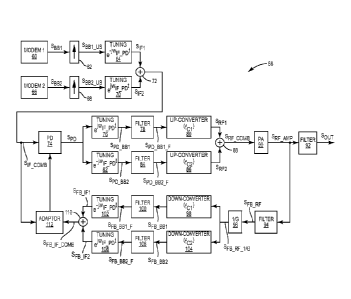
digital
predistortion, feed-forward linearization, and feedback linearization.
Predistortion
linearization uses a predefined model of power amplifier non-linearity to
generate
an "opposite" nonlinear response that compensates for the non-linearity of the
power amplifier. By amplifying the predistorted signal, the output of the
power
amplifier is as if the power amplifier were linear.
[0005] More specifically, Figure 1 illustrates a conventional
transmitter 10
without predistortion or, for that matter, any other linearization technology.
As
illustrated, the transmitter 10 includes a modem 12, an up-converter 14, a
power
amplifier (PA) 16, and a filter 18 connected as shown. The modem 12 outputs a
baseband signal (SBB) to the up-converter 14. The up-converter 14 operates to
up-convert the baseband signal (SBB) to a desired radio frequency, which is
referred to as a carrier frequency (fc), to thereby provide a radio frequency
signal
(SRF). The power amplifier 16 then amplifies the radio frequency signal (SRF)
to a
desired output power level to output an amplified radio frequency signal
(SRF AMP). Notably, as discussed below, the amplified radio frequency signal
(SRF AMP) contains distortion due to a non-linearity of the power amplifier
16. The
amplified radio frequency signal (SRF AMP) is then filtered by the filter 18
to
remove out-of-band frequency components to thereby provide an output signal
(SouT) to be transmitted by the transmitter 10.
[0006] Figures 2A through 2D are frequency band diagrams for the various
signals in the transmitter 10 of Figure 1. Specifically, Figure 2A is a
frequency
band diagram for the baseband signal (SBB). As shown, the baseband signal
(SBB) is centered at DC and has been sampled at a baseband sampling rate
(fs_BB). Figure 2B is a frequency band diagram for the radio frequency signal
(SRF) resulting from the up-conversion of the baseband signal (SBB) to the
desired
carrier frequency (fc). Importantly, Figure 2C is a frequency band diagram for
the
amplified radio frequency signal (SRF_Amp) output by the power amplifier 16.
When compared to the frequency band diagram for the radio frequency signal
CA 02821892 2013 06 14
WO 2013/046183
PCT/1B2012/055213
3
(SRF) prior to amplification as shown in Figure 2B, the frequency band diagram
of
Figure 2C clearly illustrates a frequency-spreading effect resulting from
distortion
caused by the non-linearity of the power amplifier 16. Lastly, Figure 2D is a
frequency band diagram for the output signal (Sour) output by the filter 18.
[0007] Figure 3 illustrates a conventional transmitter 20 that performs
predistortion to compensate for distortion caused by power amplifier non-
linearity. As illustrated, the transmitter 20 includes a modem 22, up-sampling
circuitry 24, a predistorter (PD) 26, an up-converter 28, a power amplifier
(PA)
30, and a filter 32 forming a forward path of the transmitter 20. The modem 22
outputs a baseband signal (SBB) to the up-sampling circuitry 24. The up-
sampling circuitry 24 up-samples the baseband signal (SBB) to a predefined
sampling rate for predistortion to thereby provide an up-sampled baseband
signal
(SBB_us). As discussed below, the sampling rate is greater than a bandwidth of
a
predistorted signal (SpD) output by the predistorter 26. The predistorter 26
predistorts the up-sampled baseband signal (SBB US) based on a defined
predistortion characteristic (e.g., an N-th order polynomial predistortion
characteristic) to provide the predistorted signal (SpD). The predistortion
applied
by the predistorter 26 compensates for (e.g., cancels or substantially
cancels) a
distortion resulting from a non-linearity of the power amplifier 30. The up-
converter 28 upconverts the predistorted signal (SpD) to a desired carrier
frequency to provide a radio frequency signal (SRF), which is then amplified
to a
desired output power level by the power amplifier 30 to provide an amplified
radio
frequency signal (SRF AMP). As a result of the predistortion applied by the
predistorter 26, the amplified radio frequency signal (SRF AMP) is as if the
power
amplifier 30 was a linear power amplifier. The filter 32 then removes any
residual
out-of-band distortion from the amplified radio frequency signal (SRF AMP) to
provide an output signal (Sour) that is transmitted by the transmitter 20.
[0008] In order to dynamically configure the predistorter 26, the
transmitter 20
also includes a feedback path including a filter 34, an attenuator 36, a down-
converter 38, and an adaptor 40 connected as shown. The filter 34 is coupled
to
the output of the power amplifier 30 and operates to remove out-of-band
CA 02821892 2013 06 14
WO 2013/046183
PCT/1B2012/055213
4
frequency components from the amplified radio frequency signal (SRF AMP) to
provide a radio frequency feedback signal (SFB_RF). The attenuator 36 then
attenuates the radio frequency feedback signal (SFB_RF) by a factor 1/G, where
G
is equal to or approximately equal to a gain of the power amplifier 30, to
thereby
provide an attenuated radio frequency feedback signal (SFB_RF_i/G). The down-
converter 38 then down-converts the attenuated radio frequency feedback signal
(SFB_RF_i/G) to baseband to provide a baseband feedback signal (SFB_BB). Based
on the baseband feedback signal (SFB_BB) and the up-sampled baseband signal
(SBB_us), the adaptor 40 dynamically configures the predistorter 26 using a
known
adaptation technique.
[0009] Figures 4A through 4E are frequency band diagrams for the various
signals in the forward path of the transmitter 20 of Figure 3. Specifically,
Figure
4A is a frequency band diagram for the baseband signal (SBB), which has a
sampling rate (fs_BB). Figure 4B is a frequency band diagram for the up-
sampled
baseband signal (SBB_us) output by the up-sampling circuitry 24, which has a
sampling rate (fs_pc), where fs_pc > fs_BB. Next, Figure 4C is a frequency
band
diagram for the predistorted signal (SpD) output by the predistorter 26. As
shown,
a frequency spreading effect results from the predistortion applied by the
predistorter 26. The sampling rate (fs_pD) is selected such that fs_pD/2 is
greater
than 1/2 of a bandwidth of the predistorted signal (SpD). Figure 4D is a
frequency
band diagram for the radio frequency signal (SRF) output by the up-converter
28.
The radio frequency signal (SRF) is centered as a desired carrier frequency
(fc)=
Lastly, Figure 4E is a frequency band diagram for the amplified radio
frequency
signal (SRF_Amp) output by the power amplifier 30. As shown, the predistortion
applied by the predistorter 26 compensates for the non-linearity of the power
amplifier 30 such that the amplified radio frequency signal (SRF_Amp) is as if
the
power amplifier 30 were a linear power amplifier.
[0010] Figures 5A through 5C are frequency band diagrams for the various
signals in the feedback path of the transmitter 20 of Figure 3. Specifically,
Figure
5A is a frequency band diagram for the radio frequency feedback signal
(SFB_RF)
output by the filter 34. Figure 5B is a frequency band diagram for the
attenuated
CA 02821892 2013 06 14
WO 2013/046183
PCT/1B2012/055213
radio frequency feedback signal (SFB_RF_1/G) output by the attenuator 36.
Lastly,
Figure 5C is a frequency band diagram for the baseband feedback signal
(SFB_BB) output by the down-converter 38.
[0011] In the transmitter 20 of Figure 3, predistortion is performed for
a single
5 band signal. However, many modern applications use dual-band signals. As
used herein, a dual-band signal is a signal that occupies two distinct
frequency
bands. More specifically, a dual-band signal contains frequency components
occupying a certain continuous bandwidth referred to as a first frequency band
and frequency components occupying another continuous bandwidth referred to
as a second frequency band. The dual-band signal contains no frequency
components between the first and second frequency bands. One exemplary
application for dual-band signals is a multi-standard cellular communication
system. A base station in a multi-standard cellular communication system may
be required to simultaneously, or concurrently, transmit signals for two
different
cellular communications protocols (i.e., transmit a dual-band signal).
Similarly, in
some scenarios, a base station in a Long Term Evolution (LTE) cellular
communications protocol may be required to simultaneously transmit signals in
separate frequency bands.
[0012] Figure 6 illustrates a conventional dual-band transmitter 42. The
dual-
band transmitter 42 includes a first modem 44 that outputs a first baseband
signal (SBB1) and a first up-converter 46 that up-converts the first baseband
signal (SBB1) to a first carrier frequency (fci) to thereby provide a first
radio
frequency signal (SRF1). The dual-band transmitter 42 also includes a second
modem 48 that outputs a second baseband signal (SBB2) and a second up-
converter 50 that up-converts the second baseband signal (SBB2) to a second
carrier frequency (fc2) to thereby provide a second radio frequency signal
(SRF2).
A combiner 52 combines the first and second radio frequency signals (SRF1 and
SRF2) to provide a combined radio frequency signal (SRF_CONAB), which is a
dual-
band signal. A power amplifier (PA) 54 then amplifies the combined radio
frequency signal (SRF_coms) to a desired output power level to thereby provide
an
amplified radio frequency signal (SRF_ANAF,), which is also a dual-band
signal. A
CA 02821892 2013 06 14
WO 2013/046183
PCT/1B2012/055213
6
filter 56 then removes out-of-band, or undesired, frequency components from
the
amplified radio frequency signal (SRF_Amp) to provide an output signal (Sour).
[0013] Figures 7A through 7G are frequency band diagrams for the various
signals in the dual-band transmitter 42 of Figure 6. Specifically, Figure 7A
is a
frequency band diagram for the first baseband signal (SBB1), where the
sampling
rate for the first baseband signal (SBB1) is fs_BB. Figure 7B is a frequency
band
diagram for the first radio frequency signal (SRF1) output by the first up-
converter
46. Likewise, Figures 7C and 7D are frequency band diagrams for the second
baseband signal (SBB2) and the second radio frequency signal (SRF2),
respectively. Figure 7E is a frequency band diagram for the combined radio
frequency signal (SRF_comB) output by the combiner 52. As illustrated, the
combined radio frequency signal (SRF_comB) is a dual-band signal having a
first
frequency band centered at the first carrier frequency (fci) and a second
frequency band centered at the second carrier frequency (fc2)=
[0014] Figure 7F is a frequency band diagram for the amplified radio
frequency signal (SRF_Amp) output by the power amplifier 54. As a result of
the
non-linearity of the power amplifier 54, a frequency-spreading effect is seen
for
the frequency bands centered at the first and second carrier frequencies (fci
and
fc2). In addition, as a result of third-order intermodulation distortion
caused by
the non-linearity of the power amplifier 54 and the dual-band nature of the
combined radio frequency signal (SRF_comB) input to the power amplifier 54,
the
amplified radio frequency signal (SRF_Amp) also includes frequency bands
centered at frequencies of 2f1-f2 and 2f2-f1. Note that, while not shown, the
combined radio frequency signal (SRF_comB) may also include higher order
intermodulation distortion. Lastly, Figure 7G is a frequency band diagram for
the
output signal (Sour), which shows that the filter 56 removed the unwanted
frequency bands (e.g., the frequency bands resulting from the third-order
intermodulation distortion centered at the frequencies of 2fc1-fc2 and 21c2-
ic1)=
[0015] Predistortion to compensate for power amplifier non-linearities
for a
dual-band transmitter presents several problems. This is particularly true if
the
dual-band transmitter is desired to include a predistorter that simultaneously
CA 02821892 2013 06 14
WO 2013/046183
PCT/1B2012/055213
7
performs predistortion for each of the frequency bands of the dual-band
signal.
As such, there is a need for systems and methods for performing predistortion
in
a dual-band transmitter.
Summary
[0016] Systems and methods for providing digital predistortion to
compensate
for a non-linearity of a power amplifier in a dual-band transmitter are
disclosed.
In one embodiment, a first baseband signal is tuned to a first intermediate
frequency to provide a first intermediate frequency signal. Likewise, a second
baseband signal is tuned to a second intermediate frequency to provide a
second
intermediate frequency signal. The first and second intermediate frequency
signals are combined to provide a combined intermediate frequency signal
having a first frequency component centered at the first intermediate
frequency
and a second frequency component centered at the second intermediate
frequency. The combined intermediate frequency signal is then predistorted to
compensate for the non-linearity of the power amplifier in the transmitter to
thereby provide a predistorted signal.
[0017] In one embodiment, a separation between the first and second
intermediate frequencies is minimized based on a target intermodulation order
(e.g., third-order intermodulation distortion, fifth-order intermodulation
distortion,
etc.) for the predistortion. More specifically, the separation between the
first and
second intermediate frequencies is minimized by being set equal to or near a
minimum separation value below which frequency bands in the predistorted
signal for up to the target intermodulation order start to overlap the
frequency
bands in the predistorted signal centered at the first and second intermediate
frequencies. By minimizing the separation between the first and second
intermediate frequencies, a sampling rate used for predistortion can be
reduced,
thereby reducing the complexity of the predistorter.
[0018] In one embodiment, the target predistortion order is the (2k+1)th-
order
where k is an integer greater than or equal to 1, and the separation between
the
first intermediate frequency and the second intermediate frequency is
minimized
CA 02821892 2013 06 14
WO 2013/046183
PCT/1B2012/055213
8
by being set equal to or near two times a minimum intermediate frequency
value.
The minimum intermediate frequency value is defined as (1/4)BW1 + (1/4)BW2 +
k*max(BWi, BW2), where k is an integer greater than or equal to 1, BWi is a
bandwidth of the first baseband signal, and BW2 is a bandwidth of the second
baseband signal. In one embodiment, the target intermodulation order is a
third-
order intermodulation. In another embodiment, the target intermodulation order
is a fifth-order intermodulation. In yet another embodiment, the target
intermodulation order is a seventh-order intermodulation.
[0019] In one embodiment, the first and second intermediate frequencies
are
symmetrical. Specifically, the first intermediate frequency is a negative
frequency, the second intermediate frequency is a positive frequency, and an
absolute value of the first intermediate frequency is equal to an absolute
value of
the second intermediate frequency. In this embodiment, when targeting the
(2k+1)th intermodulation order, the absolute value of the first and second
intermediate frequencies is set equal to or near (1/4)BW1 + (1/4)BW2 +
k*max(BWi, BW2), where k is an integer greater than or equal to 1, BWi is a
bandwidth of the first baseband signal, and BW2 is a bandwidth of the second
baseband signal.
[0020] In another embodiment, the first and second intermediate
frequencies
are asymmetrical such that the first intermediate frequency, fiF_pcu, is equal
to
-11F_PD plus a predefined frequency offset, flF_PELOFFSET, and the second
intermediate frequency, fIF_PD_23 is equal to flF_PD plus the predefined
frequency
offset, fiF_PD_OFFSET3 where flF_PD is a base intermediate frequency for
predistortion. Further, the target predistortion order is the (2k+1)th-order.
In this
embodiment, separation between the first and second intermediate frequencies
is minimized by setting the first and second intermediate frequencies such
that
the base intermediate frequency, flF_PD, is equal to or near (1/4)BW1 +
(1/4)BW2 +
k*max(BWi, BW2).
[0021] In one embodiment, prior to tuning, the first and second baseband
signals are up-sampled to a defined sampling rate for predistortion, and the
defined sampling rate is minimized based on a target predistortion order
(e.g.,
CA 02821892 2013 06 14
WO 2013/046183
PCT/1B2012/055213
9
third-order intermodulation distortion, fifth-order intermodulation
distortion, etc.).
More specifically, the defined sampling rate for predistortion is equal to or
near a
frequency below which frequency bands for the target modulation order alias
into
the frequency bands centered at the first and second intermediate frequencies
in
the predistorted signal.
[0022] In one embodiment, the first and second intermediate frequencies
are
symmetrical such that the first intermediate frequency is a negative
frequency,
the second intermediate frequency is a positive frequency, and an absolute
value
of the first intermediate frequency is equal to an absolute value of the
second
intermediate frequency. Further, the target predistortion order is the
(2k+1)th-
order. In this embodiment, the sampling rate for predistortion is minimized by
being set equal to or near (2k+2)*fiF_PD + ((k+1)/2)BW1 + ((k+1)/2)BW2 +
k*max(BWi, BW2), where k is an integer greater than or equal to 1, flF_PD is
an
absolute value of both the first and second intermediate frequencies, BWi is a
bandwidth of the first baseband signal, and BW2 is a bandwidth of the second
baseband signal. In one preferred embodiment, the absolute value of the first
and second intermediate frequencies is also minimized based on the target
predistortion order, which enables further decrease in the sampling rate for
predistortion. More specifically, when targeting the (2k+1)th-order, the
absolute
value of the first and second intermediate frequencies is minimized by being
set
equal to or near (1/4)BW1 + (1/4)BW2 + k*max(BWi, BW2).
[0023] In another embodiment, the first and second intermediate
frequencies
are asymmetrical such that the first intermediate frequency, fiF_PD_1, is
equal to -
flF_PD plus a predefined frequency offset, flF_PELOFFSET, and the second
intermediate frequency, flF_PD_23 is equal to flF_PD plus the predefined
frequency
offset, fiF2D_OFFSET, where flF_PD is a base intermediate frequency for
predistortion. Further, the target predistortion order is the (2k+1)th-order.
In this
embodiment, the sampling rate for predistortion is minimized by being set
equal
to or near (2k+2)*fiF_PD + ((k+1)/2)BW1 + ((k+1)/2)BW2 + k*max(BWi, BW2),
where k is an integer greater than or equal to 1, flF_PD is the base
intermediate
frequency for predistortion, BWi is a bandwidth of the first baseband signal,
and
CA 02821892 2013 06 14
WO 2013/046183
PCT/1B2012/055213
BW2 is a bandwidth of the second baseband signal. In one preferred
embodiment, the separation between the first and second intermediate
frequencies is also minimized based on the target predistortion order, which
enables further decrease in the sampling rate for predistortion. More
specifically,
5 when targeting the (2k+1)th-order, the separation between the first and
second
intermediate frequencies is minimized by setting the first and second
intermediate frequencies such that the base intermediate frequency, flF_PD, is
equal to or near (1/4)BW1 + (1/4)BW2 + k*max(BWi, BW2).
[0024] Those skilled in the art will appreciate the scope of the present
10 disclosure and realize additional aspects thereof after reading the
following
detailed description of the preferred embodiments in association with the
accompanying drawing figures.
Brief Description of the Drawinq Fiqures
[0025] The accompanying drawing figures incorporated in and forming a part
of this specification illustrate several aspects of the disclosure, and
together with
the description serve to explain the principles of the disclosure.
[0026] Figure 1 illustrates a conventional single-band transmitter
without
digital predistortion to compensate for power amplifier non-linearity;
[0027] Figures 2A through 2D are frequency band diagrams for the various
signals in the single-band transmitter of Figure 1;
[0028] Figure 3 illustrates a conventional single-band transmitter with
digital
predistortion to compensate for power amplifier non-linearity;
[0029] Figures 4A through 4E are frequency band diagrams for the various
signals in the forward path of the single-band transmitter of Figure 3;
[0030] Figures 5A through 5C are frequency band diagrams for the various
signals in the feedback path of the single-band transmitter of Figure 3;
[0031] Figure 6 illustrates a conventional dual-band transmitter without
digital
predistortion to compensate for power amplifier non-linearity;
[0032] Figures 7A through 7G are frequency band diagrams for the various
signals in the dual-band transmitter of Figure 6;
CA 02821892 2013 06 14
WO 2013/046183
PCT/1B2012/055213
11
[0033] Figure 8 illustrates a dual-band transmitter with digital
predistortion to
compensate for power amplifier non-linearity according to one embodiment of
the
present disclosure;
[0034] Figures 9A through 90 are frequency band diagrams for the various
signals in the forward path of the dual-band transmitter of Figure 8 according
to
one embodiment of the present disclosure;
[0035] Figures 10A through 10H are frequency band diagrams for the
various
signals in the feedback path of the dual-band transmitter of Figure 8
according to
one embodiment of the present disclosure;
[0036] Figure 11 graphically illustrates the bandwidths of the frequency
bands
in the predistorted combined radio frequency signal prior to amplification by
the
power amplifier in the dual-band transmitter of Figure 8 when targeting third-
order intermodulation distortion according to one embodiment of the present
disclosure;
[0037] Figure 12 graphically illustrates constraints for determining a
minimum
separation between the first and second intermediate frequencies for
predistortion when targeting third-order intermodulation distortion according
to
one embodiment of the present disclosure;
[0038] Figure 13 graphically illustrates frequency band overlap when the
separation between the first and second intermediate frequencies for
predistortion is less than the minimum separation determined using the
constraints illustrated in Figure 12;
[0039] Figure 14 graphically illustrates constraints for determining a
minimum
sampling rate for predistortion when targeting third-order intermodulation
distortion according to one embodiment of the present disclosure;
[0040] Figure 15 graphically illustrates the bandwidths of the frequency
bands
in the predistorted combined radio frequency signal prior to amplification by
the
power amplifier in the dual-band transmitter of Figure 8 when targeting fifth-
order
intermodulation distortion according to one embodiment of the present
disclosure;
CA 02821892 2013 06 14
WO 2013/046183
PCT/1B2012/055213
12
[0041] Figure 16 graphically illustrates constraints for determining a
minimum
separation between the first and second intermediate frequencies for
predistortion when targeting fifth-order intermodulation distortion according
to
one embodiment of the present disclosure;
[0042] Figure 17 graphically illustrates frequency band overlap when the
separation between the first and second intermediate frequencies for
predistortion is less than the minimum separation determined using the
constraints illustrated in Figure 16;
[0043] Figure 18 graphically illustrates constraints for determining a
minimum
sampling rate for predistortion when targeting fifth-order intermodulation
distortion according to one embodiment of the present disclosure;
[0044] Figure 19 graphically illustrates the bandwidths of the frequency
bands
in the predistorted combined radio frequency signal prior to amplification by
the
power amplifier in the dual-band transmitter of Figure 8 when targeting
(2k+1)th-
order intermodulation distortion according to one embodiment of the present
disclosure;
[0045] Figure 20 graphically illustrates constraints for determining a
minimum
separation between the first and second intermediate frequencies for
predistortion when targeting (2k+1)th-order intermodulation distortion
according
to one embodiment of the present disclosure;
[0046] Figure 21 graphically illustrates frequency band overlap when the
separation between the first and second intermediate frequencies for
predistortion is less than the minimum separation determined using the
constraints illustrated in Figure 20;
[0047] Figure 22 graphically illustrates constraints for determining a
minimum
sampling rate for predistortion when targeting (2k+1)th-order intermodulation
distortion according to one embodiment of the present disclosure;
[0048] Figure 23 illustrates the dual-band transmitter of Figure 8
according to
another embodiment of the present disclosure; and
[0049] Figure 24 illustrates a method of performing digital predistortion
in a
dual-band transmitter according to one embodiment of the present disclosure.
CA 02821892 2013 06 14
WO 2013/046183
PCT/1B2012/055213
13
Detailed Description
[0050] The embodiments set forth below represent the necessary
information
to enable those skilled in the art to practice the embodiments and illustrate
the
best mode of practicing the embodiments. Upon reading the following
description in light of the accompanying drawing figures, those skilled in the
art
will understand the concepts of the disclosure and will recognize applications
of
these concepts not particularly addressed herein. It should be understood that
these concepts and applications fall within the scope of the disclosure and
the
accompanying claims.
[0051] Systems and methods for providing digital predistortion to
compensate
for a non-linearity of a power amplifier in a dual-band transmitter are
disclosed.
Figure 8 illustrates an exemplary embodiment of a dual-band transmitter 58
according to one embodiment of the present disclosure. The dual-band
transmitter 58 includes a first modem 60 that outputs a first baseband signal
(SBB1). Up-sampling circuitry 62 then up-samples the first baseband signal
(SBB1)
to a predefined sampling rate for predistortion (fs_pD) to thereby provide a
first up-
sampled baseband signal (SBBLus). Notably, the up-sampling circuitry 62
preferably performs both up-sampling and image filtering. Tuning circuitry 64
then tunes the first up-sampled baseband signal (SBBLus) to a first
intermediate
frequency to provide a first intermediate frequency signal (SiFi). In a
similar
manner, a second modem 66 outputs a second baseband signal (SBB2). Up-
sampling circuitry 68 then up-samples the second baseband signal (SBB2) to the
predefined sampling rate for predistortion (fs_pD) to thereby provide an
second
up-sampled baseband signal (SBB2_us). Notably, the up-sampling circuitry 68
preferably performs both up-sampling and image filtering. Tuning circuitry 70
then tunes the second up-sampled baseband signal (SBB2_us) to a second
intermediate frequency to provide a second intermediate frequency signal
(SIF2)=
[0052] In this embodiment, the first and second intermediate frequencies
are
-IPD_IF and IPD_IF, respectively. In other words, the first intermediate
frequency is
a negative frequency, the second intermediate frequency is a positive
frequency,
CA 02821892 2013 06 14
WO 2013/046183
PCT/1B2012/055213
14
and an absolute value of both the first and second intermediate frequencies is
equal to IPD_IF. This is referred to herein as a symmetrical intermediate
frequency
embodiment. However, as discussed below, the dual-band transmitter 58 is not
limited to the use of symmetrical intermediate frequencies. In another
embodiment, asymmetrical intermediate frequencies may be used. The
asymmetrical embodiment is discussed below with respect to Figure 23.
[0053] The first and second intermediate frequency signals (SiFi and
SiF2) are
combined, or summed, by a combiner 72 to provide a combined intermediate
frequency signal (SIF_comB)= The combined intermediate frequency signal
(SIF_ComB) is a dual-band signal having a first frequency band centered at the
first
intermediate frequency, a second frequency band centered at the second
intermediate frequency, and no frequency components between the first and
second frequency bands. Also, it should be noted that the combined
intermediate frequency signal (SIF_ComB) is an equivalent baseband signal and
is
also a complex signal. A predistorter (PD) 74 then predistorts the combined
intermediate frequency signal (SIF_CONAB) to provide a predistorted signal
(SpD).
More specifically, the predistorter 74 applies a predefined predistortion to
the
combined intermediate frequency signal (SIF_CONAB) that compensates for a non-
linearity of a power amplifier in the transmit chain. The predistortion
cancels or
substantially cancels a distortion caused by the non-linearity of the power
amplifier in the transmit chain. Notably, the predistortion is performed at a
predefined sampling rate for predistortion (fs_pD). As discussed below, in one
embodiment of the present disclosure, the sampling rate for predistortion
(fs_PD)
is minimized to thereby reduce the complexity of the predistorter 74. It
should be
noted that the predistorter 74 simultaneously, or concurrently, performs
predistortion for both of the first and second baseband signals (SBBi and
SBB2)
and is therefore referred to herein as a dual-band predistorter. However,
because the input of the predistorter 74 is a single input (i.e., a single
dual-band
signal input), the predistorter 74 may use any predistortion technique
designed
for a single band input (e.g., polynomial predistortion, predistortion using a
neural
network, or the like).
CA 02821892 2013 06 14
WO 2013/046183
PCT/1B2012/055213
[0054] The predistorted signal (SpD) is then provided to tuning
circuitry 76 that
operates to tune the frequency band in the predistorted signal (SpD) that is
centered at the first intermediate frequency, which in this embodiment is -
fiF_pD,
from the first intermediate frequency to baseband to thereby provide a first
5 predistorted baseband signal (Spip_ssi). The first predistorted baseband
signal
(SpELssi) is then low-pass filtered by a filter 78 to remove unwanted
frequency
components (i.e., those frequency components that are outside of the frequency
band centered at DC), thereby providing a first filtered predistorted baseband
signal (Spip_ssi_O= An up-converter 80 then up-converts the first filtered
10 predistorted baseband signal (SpD_BB1A from baseband to a first carrier
frequency (fDi) to thereby provide a first radio frequency signal (SpF1).
Notably,
all of the processing up to the up-converter 80 is in the digital domain. As
such,
the up-converter 80 preferably also performs digital-to-analog conversion
either
at baseband or radio frequency, depending on the particular implementation.
15 [0055] In a similar manner, the predistorted signal (SpD) is also
provided to
tuning circuitry 82 that operates to tune the frequency band in the
predistorted
signal (SpD) that is centered at the second intermediate frequency, which in
this
embodiment is fiF2D, from the second intermediate frequency to baseband to
thereby provide a second predistorted baseband signal (Spip_ss2). The second
predistorted baseband signal (SpDBB2) is then low-pass filtered by a filter 84
to
remove unwanted frequency components (i.e., those frequency components that
are outside of the frequency band centered at DC), thereby providing a second
filtered predistorted baseband signal (Spip_ss2_0. An up-converter 86 then up-
converts the second filtered predistorted baseband signal (SpDBB20 from
baseband to a second carrier frequency (fD2) to thereby provide a second radio
frequency signal (SpF2). Notably, all of the processing up to the up-converter
86
is in the digital domain. As such, the up-converter 86 preferably also
performs
digital-to-analog conversion either at baseband or radio frequency, depending
on
the particular implementation.
[0056] A combiner 88 then combines, or sums, the first and second radio
frequency signals (SpFi and SRF2) to provide a combined radio frequency signal
CA 02821892 2013 06 14
WO 2013/046183
PCT/1B2012/055213
16
(SRF_CoNAB). The combined radio frequency signal (SRF_CoNAB) is a dual-band
signal having a first frequency band centered at the first carrier frequency
(fci), a
second frequency band centered at the second carrier frequency (fc2), and no
frequency components between the first and second frequency bands. In
addition, the combined radio frequency signal (SRF_comB) is a predistorted
signal.
A power amplifier (PA) 90 then amplifies the combined radio frequency signal
(SRF_coms) to a desired output power level, thereby providing an amplified
radio
frequency signal (SRF_Amp). Lastly, a filter 92 removes out-of-band frequency
components from the amplified radio frequency signal (SRF_AMP) to provide an
output signal (Sour) to be transmitted by the dual-band transmitter 58.
Specifically, the filter 92 removes any residual out-of-band distortion.
[0057] As discussed below in detail, in one embodiment, a separation
between the first and second intermediate frequencies is carefully selected to
be
at or near a minimum separation value below which frequency bands in the
predistorted signal (SpD) for third-order and, in some embodiments, higher-
order
intermodulation distortion do not overlap frequency bands in the predistorted
signal (SpD) centered at the first and second intermediate frequencies. By
doing
so, the frequency bands remain separable while at the same time the sampling
rate for predistortion (fs_pD) can be reduced. In addition to minimizing the
separation between the first and second intermediate frequencies, the sampling
rate for predistortion (fs_pD) may also be minimized by setting the sampling
rate
(fs_pD) equal to or near a minimum value below which frequency bands in the
predistorted signal (SpD) for third-order or, in some embodiments, higher-
order
intermodulation distortion alias into the frequency bands in the predistorted
signal
(SpD) centered at the first and second intermediate frequencies. Notably,
while in
the preferred embodiment both the separation between the first and second
intermediate frequencies and the sampling rate (fs_pD) are minimized, the
separation between the first and second intermediate frequencies may be
minimized without minimizing the sampling rate (fs_pD), and the sampling rate
(fs_pD) may be minimized without minimizing the separation between the first
and
second intermediate frequencies.
CA 02821892 2013 06 14
WO 2013/046183
PCT/1B2012/055213
17
[0058] The dual-band transmitter 58 also includes a feedback path
including a
filter 94 that filters the amplified radio frequency signal (SRF_AMP) from the
output
of the power amplifier 90 to remove any residual out-of-band distortion to
provide
a radio frequency feedback signal (SFB_RF). The radio frequency feedback
signal
(SFB_RF) is attenuated by an attenuator 96 to provide an attenuated radio
frequency feedback signal (SFB_RF_i/G). A down-converter 98 down-converts the
attenuated radio frequency feedback signal (SFB_RF_i/G) such that the
frequency
band centered at the first carrier frequency (fci) is now at baseband, thereby
providing a first baseband feedback signal (SFB_BB1). A filter 100 then low-
pass
filters the first baseband feedback signal (SFB_BB1) to remove the unwanted
frequency bands (i.e., the frequency bands other than that centered at DC).
Tuning circuitry 102 then tunes the first baseband feedback signal (SFB_BB1)
to
the first intermediate frequency, which in this embodiment is -fiF_Fo, thereby
providing a first intermediate frequency feedback signal (SFB_IF1). The first
intermediate frequency feedback signal (SFB _IR) is a counter-part signal to
the
first intermediate frequency signal (SiFi) in the forward path of the dual-
band
transmitter 58.
[0059] In a similar manner, a down-converter 104 down-converts the
attenuated radio frequency feedback signal (SFB_RF_i/G) such that the
frequency
band centered at the second carrier frequency (fo2) is now at baseband,
thereby
providing a second baseband feedback signal (SFB_BB2). A filter 106 then low-
pass filters the second baseband feedback signal (SR3_13132) to remove the
unwanted frequency bands (i.e., the frequency bands other than that centered
at
DC). Tuning circuitry 108 then tunes the second baseband feedback signal
(SFB_BB2) to the second intermediate frequency, which in this embodiment is
flF_PD, thereby providing a second intermediate frequency feedback signal
(SFB _IF2). The second intermediate frequency feedback signal (SFB JF2) is a
counter-part signal to the second intermediate frequency signal (S1F2) in the
forward path of the dual-band transmitter 58.
[0060] A combiner 110 then combines, or sums, the first and second
intermediate frequency feedback signals (SFB Fl and SFB 1F2) to provide a
CA 02821892 2013 06 14
WO 2013/046183
PCT/1B2012/055213
18
combined intermediate frequency feedback signal (SFBJF_COMB). An adaptor 112
then dynamically configures the predistorter 74 based on the combined
intermediate frequency feedback signal (SFB_IF_COMB) and the combined
intermediate frequency signal (SIF_Coms). Specifically, the adaptor 112
updates
one or more predistortion parameters (e.g., polynomial coefficients defining a
polynomial predistortion) using any suitable predistortion adaptation
algorithm.
[0061] Figures 9A through 90 are frequency band diagrams for the various
signals in the forward path of the dual-band transmitter 58 of Figure 8.
Notably,
in Figures 9A through 90 the target intermodulation order for the
predistortion is
the third-order (i.e., IM3). However, it is to be appreciated that the target
intermodulation order for the predistortion may be the (2k+1)th order where k
is
an integer greater than or equal to 1. Figure 9A is a frequency band diagram
for
the first baseband signal (SBB1). As shown, the sampling rate for the first
baseband signal (SBB1) is fs_ssi. Figure 9B is a frequency band diagram for
the
first up-sampled baseband signal (Smi_us). As shown, the sampling rate for the
first up-sampled baseband signal (Smi_us) is the sampling rate for
predistortion
(fs_pD). Figure 9C is a frequency band diagram for the first intermediate
frequency signal (SiFi). As shown, the first intermediate frequency signal
(SiFi) is
centered at the first intermediate frequency, which in this embodiment is -
fiF_RD.
In a similar manner, Figures 9D through 9F are frequency band diagrams for the
second baseband signal (Sss2), the second up-sampled baseband signal
(SBB2_us), and the second intermediate frequency signal (SIF2)=
[0062] Figure 9G is a frequency band diagram for the combined
intermediate
frequency signal (SIF_coms). As shown, the combined intermediate frequency
signal (SIF_comB) is a dual-band signal having a first frequency band centered
at
the first intermediate frequency, which in this embodiment is -fiF_pD; a
second
frequency band centered at the second intermediate frequency, which in this
embodiment is flF_PD; and no frequency components between the first and
second frequency bands. Also, the combined intermediate frequency signal
(SIF_coms) is an equivalent baseband signal and is also a complex signal.
Figure
9H is a frequency band diagram for the predistorted signal (SpD). As
illustrated,
CA 02821892 2013 06 14
WO 2013/046183
PCT/1B2012/055213
19
the predistortion results in a frequency-spreading effect for the frequency
bands
centered at the first and second intermediate frequencies.
[0063] Figure 91 is a frequency band diagram for the first predistorted
baseband signal (SRD_BBi) output by the tuning circuitry 76. As shown, the
frequency band in the predistorted signal (SpD) centered at the first
intermediate
frequency is now at baseband (i.e., centered at DC). Figure 9J is a frequency
band diagram for the first filtered predistorted baseband signal (SRD_BBLF).
As
shown, the first predistorted baseband signal (SpD_BB1) is low-pass filtered
to
remove the unwanted frequency components, which in this case are the
frequency components other than those in the frequency band centered at DC.
Figure 9K is a frequency band diagram for the first radio frequency signal
(SRF1).
As shown, the first filtered predistorted baseband signal (SpD_BB1A is up-
converted to the first carrier frequency (fci). In a similar manner, Figures
9L
through 9N are frequency band diagrams for the second predistorted baseband
signal (SPD_BB2), the second filtered predistorted baseband signal (SPD_BB2A,
and
the second radio frequency signal (SRF2).
[0064] Figure 90 is a frequency band diagram for the combined radio
frequency signal (SRF_comB) output by the combiner 88. As shown, the combined
radio frequency signal (SRF_comB) is a dual-band signal having a first
frequency
band centered at the first carrier frequency (fci), a second frequency band
centered at the second carrier frequency (fo2), and no frequency components
between the first and second frequency bands. Figure 9P is a frequency band
diagram for the amplified radio frequency signal (SRF_AMP) output by the power
amplifier 90. As shown, the predistortion for the frequency bands centered at
the
first and second carrier frequencies (foi and fo2) cancels the distortion
caused by
the non-linearity of the power amplifier 90 for the corresponding frequency
bands. However, due to intermodulation distortion, residual out-of-band
distortion remains in the frequency band centered at 2f1-f2 and 2f2-f1. This
residual out-of-band distortion is removed by the filter 92 as shown in the
frequency band diagram for the output signal (Sour) shown in Figure 90.
CA 02821892 2013 06 14
WO 2013/046183
PCT/1B2012/055213
[0065] Figures 10A through 10H are frequency band diagrams for the
various
signals in the feedback path of the dual-band transmitter 58 of Figure 8.
Specifically, Figure 10A is a frequency band diagram for the attenuated radio
frequency feedback signal (SFB_RF_1/G) output by the attenuator 96. Figure 10B
is
5 a frequency band diagram for the first baseband feedback signal (SFB_BB1)
output
by the down-converter 98. As shown, the first baseband feedback signal
(SFB_BB1) includes frequency components in a frequency band centered at DC as
well as frequency components in a frequency band centered at f2-f1. After low-
pass filtering by the filter 100, the resulting first filtered baseband
feedback signal
10 (SFB_BBLF) includes only the frequency components in the frequency band
centered at DC, as illustrated in Figure 10C. Figure 10D is a frequency band
diagram for the first intermediate frequency feedback signal (SFB_Fi) output
by
the tuning circuitry 102. As illustrated, the tuning circuitry 102 moves the
frequency band centered at DC in the first filtered baseband feedback signal
15 (SFB_BBi_F) to the first intermediate frequency, which in this
embodiment is -fiF_RD.
[0066] Figure 10E is a frequency band diagram for the second baseband
feedback signal (SFB_BB2) output by the down-converter 104. As shown, the
second baseband feedback signal (SFB_BB2) includes frequency components in a
frequency band centered at DC as well as frequency components in a frequency
20 band centered at -(fc2-fc1). After low-pass filtering by the filter 106,
the resulting
second filtered baseband feedback signal (SFB_BB2_F) includes only the
frequency
components in the frequency band centered at DC, as illustrated in Figure 10F.
Figure 10G is a frequency band diagram for the second intermediate frequency
feedback signal (SFB_IF2) output by the tuning circuitry 108. As illustrated,
the
tuning circuitry 108 moves the frequency band centered at DC in the second
filtered baseband feedback signal (SFB_BB2_F) to the second intermediate
frequency, which in this embodiment is fiF2D. Lastly, Figure 10H is a
frequency
band diagram for the combined intermediate frequency feedback signal
(SFB JF_comB) output by the combiner 110.
[0067] Now that the dual-band transmitter 58 and the operation thereof have
been described, attention will now turn to embodiments wherein the separation
CA 02821892 2013 06 14
WO 2013/046183
PCT/1B2012/055213
21
between the first and second intermediate frequencies and/or the sampling rate
for predistortion (fs_pc) are minimized. Figures 11 through 14 graphically
illustrate the manner in which the separation between the first and second
intermediate frequencies and the sampling rate for predistortion can be
minimized when targeting third-order intermodulation distortion (IM3).
Specifically, Figure 11 first illustrates the frequency bands in the combined
radio
frequency signal (SRF_coms) when targeting third-order intermodulation
distortion
according to one embodiment of the present disclosure. As a result of the
predistortion applied by the predistorter 74, frequency-band spreading has
occurred for the primary frequency bands at the first and second carrier
frequencies (fci and fci). In addition, the combined radio frequency signal
(SRF_coms) includes frequency components in frequency bands centered at 2fc1-
fc2 and 21c2-ic1 due to intermodulation distortion.
[0068] The bandwidths of the frequency bands in the combined radio
frequency signal (SRF_coms) were determined using a four-tone analysis.
Specifically, the first and second baseband signals (Sssi and SI3132) were
each
modeled by two tones. The first baseband signal (Sssi) was modeled by a first
tone on a left-most edge of the corresponding frequency band and a second tone
on a right-most edge of the corresponding frequency band. Likewise, the second
baseband signal (Sss2) was modeled by a first tone on a left-most edge of the
corresponding frequency band and a second tone on a right-most edge of the
corresponding frequency band. Using this four-tone analysis, the bandwidth of
the four frequency bands (referred to as frequency bands A through D) were
determined as follows:
= Frequency Band A: The bandwidth of the frequency band centered
at the first carrier frequency (fci), which is referred to herein as
frequency band A, has a bandwidth (BWim3_,a) defined as:
BW,,,,,,3 A = BW, +2max(BWI,BW2), (1)
where BWi is a bandwidth of the first baseband signal (Sssi) and
BW2 is a bandwidth of the second baseband signal (Sss2);
CA 02821892 2013 06 14
WO 2013/046183
PCT/1B2012/055213
22
= Frequency Band B: The bandwidth of the frequency band centered
at the second carrier frequency (fc2), which is referred to herein as
frequency band B, has a bandwidth (BWim3 _B) defined as:
BWD,,3 B = BW2 + 2 max(BWI , BW2 ); (2)
= Frequency Band C: The bandwidth of the frequency band centered
at 2f1-f2, which is referred to herein as frequency band C, has a
bandwidth (BWim3_c) defined as:
BW/m3 c = 2BW1 + BW2; and (3)
= Frequency Band D: The bandwidth of the frequency band centered
at 21c2-ic1, which is referred to herein as frequency band D, has a
bandwidth (BWim3JD) defined as:
BW/m3 D = BW, +2BW2. (4)
[0069] Figure 12 graphically illustrates the manner in which a minimum
intermediate frequency value, fiF_PD_NAIN, is determined when targeting third-
order
intermodulation distortion based on the bandwidths of the frequency bands A
through D according to one embodiment of the present disclosure. In this
embodiment, the first and second intermediate frequencies are -1IF_PD and
fIF_PD)
respectively. As such, when targeting third-order intermodulation distortion,
the
four frequency bands A through D in the predistorted signal (SpD) output by
the
predistorter 74 are centered at -11F _PD) flF_PD, -31IF_PD, and 3fIF_PD,
respectively. As
illustrated, in order to maintain separation between the four frequency bands
A
through D, the following constraints must be met:
= Constraint A: In order to maintain separation between frequency
bands A and C, the following must be true:
1 i
¨2f BWIM3 C BW im 3 A) .
IF PD MIN (5)
2
= Constraint B: In order to maintain separation between frequency
bands A and B, the following must be true:
,, 1 (now
2 f IF PD MIN .-- -2k" Yr IM3 A BW IM 3 B) ' (6)
CA 02821892 2013 06 14
WO 2013/046183
PCT/1B2012/055213
23
= Constraint C: In order to maintain separation between frequency
bands B and D, the following must be true:
1
2fIF PD MIN i ¨2/314/1M3 B + BWIM3 D)' (7)
[0070] From Equation (5) ¨ Equation (7),
f IF PD MIN = 1 ¨4maxAkk-BW/m3 c BW/M3 A),(13WIM3 A BWIM3 B),(BWIM3 B
BWIM3 A ' (8)
Substituting Equation (1) ¨ Equation (4) into Equation (8) gives:
f IF PD MIN = ¨1BW ¨1BW 2 max(BW1, BW 2) . (9)
4 4
Further, if BWi BW2, Equation (9) takes the form:
f IF PD MIN = ¨4" Yr . 1 -Dw4" Yr 2 ' (10)
10 Similarly, if BWi = BW2, Equation (9) takes the form:
3 w
f IF PD MIN =no, ¨2" Yri ' (1 1 )
[0071] Assuming a sufficiently large sampling rate for predistortion
(fs_pD), the
separation between the first and second intermediate frequencies can be
minimized based on Equation (9) ¨ Equation (11). More specifically, in this
15 embodiment, the first and second intermediate frequencies are -11F_PD
and f IF_PD,
respectively. The separation between the first and second intermediate
frequencies can therefore be minimized by setting flF_PD equal to or near the
minimum intermediate frequency value (f IF_PD_MIN) such that the separation
between the first and second intermediate frequencies is at or near
211F_PD_MIN.
More specifically, in one embodiment, the first intermediate frequency, which
in
this embodiment is -fiF2D, is a frequency in the range of and including -
11F_PD_MIN
and -211F_PD_MIN, and the second intermediate frequency, which in this
embodiment is fiF2D, is a frequency in the range of and including fiFiDELNAIN
and
2fiF_pp_miN. In this manner, the separation between the first and second
intermediate frequencies is in the range of and including 2fiF_PD_miN and
4fiF_PD_MIN=
CA 02821892 2013 06 14
WO 2013/046183
PCT/1B2012/055213
24
[0072] In another embodiment, the first intermediate frequency, which in
this
embodiment is -11F _PD, is a frequency equal to -11F_PD_MIN minus a predefined
guard
band, and the second intermediate frequency, which in this embodiment is
fiF2D,
is a frequency equal to flF_PD_MIN plus the predefined guard band. The
predefined
guard band is a predetermined guard band of a size providing sufficient
separation between the frequency bands A through D to allow proper filtering
by
the filters 78 and 84.
[0073] Figure 13 is a frequency band diagram for the output of the
predistorter
74 in a situation where the separation between the first and second
intermediate
frequencies is less than the minimum separation, which as discussed above is
2fiF_pD_NniN. As illustrated, there is overlap between frequency bands C and
A,
between frequency bands A and B, and between frequency bands B and D. This
overlap degrades the performance of the dual-band transmitter 58 and, as such,
is not desirable. As discussed above, in the preferred embodiment, the first
and
second intermediate frequencies are carefully selected such that the
separation
between the first and second intermediate frequencies is at or near the
minimum
separation, which is 2fiF_IPD_NniN. In this manner, overlap between the
frequency
bands A through D is avoided, but, at the same time, the separation between
the
first and second intermediate frequencies is minimized. This minimization of
the
separation between the first and second intermediate frequencies reduces the
sampling rate for predistortion (fs_pD), which in turn reduces the complexity
of the
predistorter 74.
[0074] Figure 14 graphically illustrates the manner in which the
sampling rate
for predistortion (fs_pD) is minimized when targeting third-order
intermodulation
distortion (IM3) according to one embodiment of the present disclosure. In
general, aliasing of the frequency components in the frequency bands A through
D constrains minimization of the sampling rate for predistortion (fs_pD).
Specifically, looking at Figure 14, due to aliasing, a first image of the
frequency
bands A through D is centered at -fs_pD, and a second image of the frequency
bands A through D is centered at fs_pD. A minimum sampling rate for
predistortion (fs_pD_miN) is a sampling rate below which the frequency band D
in
CA 02821892 2013 06 14
WO 2013/046183
PCT/1B2012/055213
the first image aliases into the frequency band A and the frequency band C in
the
second image aliases into the frequency band B. In other words, the
constraints
for the minimum sampling rate for predistortion (fs_pp_miN) are:
= Constraint A: In order to prevent aliasing of the frequency band D
5 into the frequency band A, the following must be true:
1 I
fS PD MIN ¨ 4fIF-PD ¨2WWIM 3 D + BWIM3 A) ' (12)
= Constraint B: In order to prevent aliasing of the frequency band C
into the frequency band B, the following must be true:
1 I
fS PD MIN ¨ 4fIF-PD ¨2WWIM3 C + BWIM3 B) ' (13)
10 [0075] From Equation (12) and Equation (13),
f S PD MIN = 4 f IF PD +i2 max ((B W im 3 D BW im3 A ), (B Wim 3 c BW im3
B)) (14)
Substituting Equation (1) ¨ Equation (4) into Equation (14) gives:
fs pp mIN = 4LF BD BW BW 2 max(BW 1 , BW2 ) . (15)
If flF_PD = flF_PD_MIN, Equation (15) takes the form:
15 f S PD MIN = 2B-14 /1+ 2BW 2 5 max (BW, , BW2 ) . (16)
Further, if BWi BW2, Equation (16) takes the form:
f S PD MIN =2BW1+7BW2. (17)
Similarly, if BWi = BW2, Equation (16) takes the form:
fs PD MIN = 9BWI = (18)
20 [0076]
The sampling rate for predistortion (fs_pD) when targeting third-order
intermodulation distortion can be minimized based on Equation (15) ¨ Equation
(18). More specifically, in one embodiment, the sampling rate for
predistortion
(fs_pD) is set equal to or near the minimum sampling rate for predistortion
(fs_pp_miN). In one particular embodiment, the sampling rate for predistortion
25 (fs_pD) is set to a sampling rate in the range of and including
fS_PD_MIN and
2fs_pp_miN. In this manner, aliasing of the frequency band C in the second
image
into the frequency band B and aliasing of the frequency band D in the first
image
into the frequency band A is avoided.
CA 02821892 2013 06 14
WO 2013/046183
PCT/1B2012/055213
26
[0077] Figures 15 through 18 graphically illustrate the manner in which
the
separation between the first and second intermediate frequencies and the
sampling rate for predistortion can be minimized when targeting fifth-order
intermodulation distortion (IM5). Specifically, Figure 15 first illustrates
the
frequency bands in the combined radio frequency signal (SRF_comB) when
targeting fifth-order intermodulation distortion according to one embodiment
of
the present disclosure. As a result of the predistortion applied by the
predistorter
74, frequency-band spreading has occurred for the primary frequency bands at
the first and second carrier frequencies (fci and fci). In addition, the
combined
radio frequency signal (SRF_comB) includes frequency components in frequency
bands centered at 2fc1-ic2, 2fc2-fc1, 31c1-21c2, and 3fc2-2fc1 due to
intermodulation
distortion.
[0078] The bandwidths of the frequency bands in the combined radio
frequency signal (SRF_comB) were determined using a four-tone analysis.
Specifically, the first and second baseband signals (SBB1 and SBB2) were each
modeled by two tones. The first baseband signal (SBB1) was modeled by a first
tone on a left-most edge of the corresponding frequency band and a second tone
on a right-most edge of the corresponding frequency band. Likewise, the second
baseband signal (SBB2) was modeled by a first tone on a left-most edge of the
corresponding frequency band and a second tone on a right-most edge of the
corresponding frequency band. Using this four-tone analysis, the bandwidth of
the six frequency bands (referred to as frequency bands A through F) were
determined as follows:
= Frequency Band A: The bandwidth of the frequency band centered
at the first carrier frequency (fci), which is referred to herein as
frequency band A, has a bandwidth (BWims_A) defined as:
BW,,,,,,5 A = BW, + 4 max(BWI , BW2 ) , (19)
where BWi is a bandwidth of the first baseband signal (SBB1) and
BW2 is a bandwidth of the second baseband signal (SBB2);
CA 02821892 2013 06 14
WO 2013/046183
PCT/1B2012/055213
27
= Frequency Band B: The bandwidth of the frequency band centered
at the second carrier frequency (fc2), which is referred to herein as
frequency band B, has a bandwidth (BWims_B) defined as:
BWõ,,,5 , = BW2 + 4 max(BW , BW2 ) ; (20)
= Frequency Band C: The bandwidth of the frequency band centered
at 2f1-f2, which is referred to herein as frequency band C, has a
bandwidth (BWims_c) defined as:
BWim5 , = 2BW + BW2 + 2 max(BW , BW2 ); (21)
= Frequency Band D: The bandwidth of the frequency band centered
at 21c2-ic1, which is referred to herein as frequency band D, has a
bandwidth (BWims_D) defined as:
BWõ,,,5 , = BW, + 2BW2 + 2 max(BW , BW2 ); (22)
= Frequency Band E: The bandwidth of the frequency band centered
at 3fc1-21c2, which is referred to herein as frequency band E, has a
bandwidth (BWims_E) defined as:
BWõ,,5 , =3BW, + 2BW2 ; and (23)
= Frequency Band F: The bandwidth of the frequency band centered
at 3f2-2f1, which is referred to herein as frequency band F, has a
bandwidth (BWims_F) defined as:
BWõ,,5 , = 2BW, +3BW2. (24)
[0079] Figure 16 graphically illustrates the manner in which a minimum
intermediate frequency value, flF_PD_NAIN) is determined when targeting fifth-
order
intermodulation distortion based on the bandwidths of the frequency bands A
through F according to one embodiment of the present disclosure. In this
embodiment, the first and second intermediate frequencies are -1IF_PD and
fIF_PD)
respectively. As such, when targeting fifth-order intermodulation distortion,
the
six frequency bands A through F in the predistorted signal (SpD) output by the
predistorter 74 are centered at -11F _PD) flF_PD, -311F _PD) 311F _PD, -511F
2D) and 511F_PD)
respectively. As illustrated, in order to maintain separation between the six
frequency bands A through F, the following constraints must be met:
CA 02821892 2013 06 14
WO 2013/046183
PCT/1B2012/055213
28
= Constraint A: In order to maintain separation between frequency
bands A and C, the following must be true:
1 i
2 ¨f BWIM 5 C BWim5 A).
IF PD MIN (25)
2
= Constraint B: In order to maintain separation between frequency
bands A and B, the following must be true:
1
2fIF PD MIN i ¨ 131/1/IM 5 A + BWIM 5 B)= (26)
2
= Constraint C: In order to maintain separation between frequency
bands B and D, the following must be true:
1
2fIF PD MIN i ¨213WIM 5 B + B1/1/ 1m 5 D) (27)
Notably, there are no constraints for the separation between the frequency
bands
E and C and the frequency bands D and F because overlap between these
frequency bands is of no concern. Only overlap with the primary frequency
bands, or useable, frequency bands A and B is of concern.
[0080] From Equation (25) ¨ Equation (27),
f IF PD MIN = 1 ¨4 ma(nw
AW-' "IM5 C BWIM5 A)5(13WIM5 A BWIM5 B)5(13WIM5 B BWIM5 D)). (28)
Substituting Equation (19) ¨ Equation (22) into Equation (28) gives:
f IF PD MIN = ¨1 MK + ¨1 BW 2 + 2 max(BW, 5 BW2 ) . (29)
4 4
Further, if BWi BW2, Equation (29) takes the form:
9
fIF PD MIN = 1 ¨4"--' vr pw 1 pw ¨4-i--' vr 2 ' (30)
Similarly, if BWi = BW2, Equation (29) takes the form:
5
f IF PD MIN =n,,,w ¨2- Yr 1 ' (31)
[0081] Assuming a sufficiently large sampling rate for predistortion
(fs_pD), the
separation between the first and second intermediate frequencies can be
minimized based on Equation (29) ¨ Equation (31). More specifically, in this
embodiment, the first and second intermediate frequencies are -fiF_pD and
flF_PD,
CA 02821892 2013 06 14
WO 2013/046183
PCT/1B2012/055213
29
respectively. The separation between the first and second intermediate
frequencies can therefore be minimized by setting flF_PD equal to or near the
minimum intermediate frequency value (fIF_PD_MIN) such that the separation
between the first and second intermediate frequencies is at or near 211F
PD_MIN=
More specifically, in one embodiment, the first intermediate frequency, which
in
this embodiment is -11F 2D, is a frequency in the range of and including -
11F_PD_MIN
and -211F_PD_MIN, and the second intermediate frequency, which in this
embodiment is fiF2D, is a frequency in the range of and including fiFiDELNAIN
and
211F_pp_miN. In this manner, the separation between the first and second
intermediate frequencies is in the range of and including 211F_PD_NniN and
411F_PD_MIN=
[0082] In another embodiment, the first intermediate frequency, which in
this
embodiment is 41F _PD, is a frequency equal to -11F_PD_MIN minus a predefined
guard
band, and the second intermediate frequency, which in this embodiment is
fiF2D,
is a frequency equal to flF_PD_MIN plus the predefined guard band. The
predefined
guard band is a predetermined guard band of a size providing sufficient
separation between the frequency bands A through D to allow proper filtering
by
the filters 78 and 84.
[0083] Figure 17 is a frequency band diagram for the output of the
predistorter
74 in a situation where the separation between the first and second
intermediate
frequencies is less than the minimum separation, which as discussed above is
211F_pp_miN. As illustrated, there is overlap between frequency bands C and A,
between frequency bands A and B, and between frequency bands B and D. This
overlap degrades the performance of the dual-band transmitter 58 and, as such,
is not desirable. Notably, the overlap between frequency bands E and C and
between frequency bands D and F is of no concern. Rather, only the overlaps
involving the primary, or usable, frequency bands A and B are of concern. As
discussed above, in the preferred embodiment, the first and second
intermediate
frequencies are carefully selected such that the separation between the first
and
second intermediate frequencies is at or near the minimum separation, which is
211F_pp_miN. In this manner, overlap between the frequency bands A through D
is
CA 02821892 2013 06 14
WO 2013/046183
PCT/1B2012/055213
avoided, but, at the same time, the separation between the first and second
intermediate frequencies is minimized This minimization of the separation
between the first and second intermediate frequencies reduces the sampling
rate
for predistortion (fs_pD), which reduces the complexity of the predistorter
74.
5 [0084] Figure 18 graphically illustrates the manner in which the
sampling rate
for predistortion (fs_pD) is minimized when targeting fifth-order
intermodulation
distortion (IM5) according to one embodiment of the present disclosure. In
general, aliasing of the frequency components in the frequency bands A through
F constrains minimization of the sampling rate for predistortion (fs_PD)=
10 Specifically, looking at Figure 18, due to aliasing, a first image of
the frequency
bands A through F is centered at -fs_pD, and a second image of the frequency
bands A through F is centered at is_pD. The minimum sampling rate for
predistortion (fs_pp_miN) is a frequency below which the frequency band F in
the
first image aliases into the frequency band A and the frequency band E in the
15 second image aliases into the frequency band B. In other words, the
constraints
for the minimum sampling rate for predistortion (fs_pp_miN) are:
= Constraint A: In order to prevent aliasing of the frequency band F
into the frequency band A, the following must be true:
1 I
fS PD MIN ¨ 6fIF-PD ¨2WWIM 5 F + BWIM 5 A) ' (32)
20 =
Constraint B: In order to prevent aliasing of the frequency band E
into the frequency band B, the following must be true:
1
f I
BW
¨6f ¨ im 5 E BW/M5) ' B
S PD MIN IF-PD 2 (33)
[0085] From Equation (32) and Equation (33),
f S PD MIN = 6 f IF PD -1
2max0W im5 F BW im5 A ), (B Wim 5 E BW im5 B)) (34)
25 Substituting Equation (19) ¨ Equation (24) into Equation (34) gives:
f S PD MIN = 6 f IF-PD ¨23 B14/1 + ¨3 BW2 + 2 max(BW 5 BW2 ) . (35)
2
If flF_PD = flF_PD_MIN, Equation (35) takes the form:
CA 02821892 2013 06 14
WO 2013/046183
PCT/1B2012/055213
31
f S PD MIN = 3BW 3BW 2 +14 max(BW , BW2 ) . (36)
Further, if BWi BW2, Equation (36) takes the form:
f S PD MIN = 3BW +17 BW 2. (37)
Similarly, if BWi = BW2, Equation (36) takes the form:
f S PD MIN = 20BW 1 . (38)
[0086] The sampling rate for predistortion (fs_pD) when targeting fifth-
order
intermodulation distortion can be minimized based on Equation (35) ¨ Equation
(38). More specifically, in one embodiment, the sampling rate for
predistortion
(fs_pD) is set equal to or near the minimum sampling rate for predistortion
(fs_pp_miN)= In one particular embodiment, the sampling rate for predistortion
(fs_pD) is set to a sampling rate in the range of and including IS_PD_MIN and
2fs_pp_miN. In this manner, aliasing of the frequency band E in the second
image
into the frequency band B and aliasing of the frequency band F in the first
image
into the frequency band A is avoided.
[0087] Figures 19 through 22 graphically illustrate the manner in which the
separation between the first and second intermediate frequencies and the
sampling rate for predistortion can be minimized when targeting (2k+1)th-order
intermodulation distortion where k is an integer greater than or equal to 1.
In
other words, Figures 19 through 22 are a generalization for targeting any
desired
order of intermodulation distortion. Specifically, Figure 19 first illustrates
the
frequency bands in the combined radio frequency signal (SRF_coms) when
targeting the (2k+1)th order intermodulation distortion according to one
embodiment of the present disclosure. As a result of the predistortion applied
by
the predistorter 74, frequency-band spreading has occurred for the primary
frequency bands at the first and second carrier frequencies (fci and fc2). In
addition, the combined radio frequency signal (SRF_comB) includes frequency
components in frequency bands centered at 2fc1-fc2, 2fc2-fc1, ..., kfc1-(k-
1)1c2,
kfc2-(k-1)fc1, (k+1)fc1-kfc2, and (k+1)fc2-kfc1 due to intermodulation
distortion.
[0088] The bandwidths of the frequency bands in the combined radio
frequency signal (SRF_comB) were determined using a four-tone analysis.
CA 02821892 2013 06 14
WO 2013/046183
PCT/1B2012/055213
32
Specifically, the first and second baseband signals (SBB1 and SB132) were each
modeled by two tones. The first baseband signal (SBB1) was modeled by a first
tone on a left-most edge of the corresponding frequency band and a second tone
on a right-most edge of the corresponding frequency band. Likewise, the second
baseband signal (SB2) was modeled by a first tone on a left-most edge of the
corresponding frequency band and a second tone on a right-most edge of the
corresponding frequency band. Using this four-tone analysis, the bandwidth of
the frequency bands (referred to as frequency bands 1 through 2k+2) were
determined to be:
= Frequency Band 2i+1 centered at (i+1)1c1 ¨ ifc2:
BW/m (2k+1) _(2i+1) = (i 1)BW iBW2 2(k - i ) = max(BW , BW2 ) , (39)
where i is an integer greater than or equal to 0, BWi is a bandwidth
of the first baseband signal (SBB1), and BW2 is a bandwidth of the
second baseband signal (SBB2).
= Frequency Band 2i+2 centered at (i+1)1c2¨ ifci:
BW/m(2k+i) (2i+2) = (i 1)BW2 iBW 2(k - i) = max(BW , BW2 ). (40)
[0089] Figure 20 graphically illustrates the manner in which a minimum
intermediate frequency value, flF_PD_MIN, is determined when targeting the
(2k+1)th-order intermodulation distortion based on the bandwidths of the
frequency bands 1 through 2k+2 according to one embodiment of the present
disclosure. In this embodiment, the first and second intermediate frequencies
are -11F_PD and flF_PD, respectively. As such, when targeting the (2k+1)th-
order
intermodulation distortion, the frequency bands in the predistorted signal
(SpD)
output by the predistorter 74 are centered at fIF_PD, 311F _PD, 511F _PD,
etc. As
illustrated, in order to maintain separation between the frequency bands, the
following constraints must be met:
= Constraint A: In order to maintain separation between frequency
bands 1 and 3, the following must be true:
1 (Du]
2 f IF PD MIN -2 \ " " im (2k+1)_ 03 BW/M(2k+1) 01 ) ' (41)
CA 02821892 2013 06 14
WO 2013/046183
PCT/1B2012/055213
33
= Constraint B: In order to maintain separation between frequency
bands 1 and 2, the following must be true:
...., 1 (Du]
2 f IF PD MIN .-- ¨2 kl" " im (2k+1) 01 BW/M (2k+1)_ 02 )' (42)
= Constraint C: In order to maintain separation between frequency
bands 2 and 4, the following must be true:
...., (Du] 1
2 f IF PD MIN .-- ¨2 kl" " im (2k+1) _ 02 BW/M(2k+1) 04 ) ' (43)
Notably, there are no constraints for the separation between the other
frequency
bands because overlap between these frequency bands is of no concern. Only
overlap with the primary, or useable, frequency bands 1 and 2 is of concern.
[0090] From Equation (41) ¨ Equation (43),
f IF PD MIN = 1max((B WE, (2k+1) 03 BW/M(2k+1) 01 )5
4 (44)
(B4//m(2k+1) oi BW/m (2k+1) 02 )5 (BW/M (2k+1) 02 BW/M(2k+1) 04 ))
Substituting Equation (39) ¨ Equation (40) into Equation (44) gives:
f IF PD MIN = 1 ¨4" Y Y nõ,,, 1 1 -4" " Du, 2 k = max(BW , BW2 ) . (45)
Further, if BWi BW2, Equation (45) takes the form:
1 0
1
f IF PD MIN = ¨ BW 1 + k+¨ BW2. (46)
4 \,. 4 j
Similarly, if BWi = BW2, Equation (45) takes the form:
1 0
f IF PD MIN = k+¨ MK. (47)
\,. 2,
[0091] Assuming a sufficiently large sampling rate for predistortion
(fs_pD), the
separation between the first and second intermediate frequencies can be
minimized based on Equation (44) ¨ Equation (47). More specifically, in this
embodiment, the first and second intermediate frequencies are -11F_PD and
fIF_PD)
respectively. The separation between the first and second intermediate
frequencies can therefore be minimized by setting flF_PD equal to or near the
minimum intermediate frequency value (f IF_PD_MIN) such that the separation
between the first and second intermediate frequencies is at or near
211F2ELmiN=
CA 02821892 2013 06 14
WO 2013/046183
PCT/1B2012/055213
34
More specifically, in one embodiment, the first intermediate frequency, which
in
this embodiment is -fiF2D, is a frequency in the range of and including -
11F_PD_MIN
and -211F_PD_MIN, and the second intermediate frequency, which in this
embodiment is fiF2D, is a frequency in the range of and including fiFiDELNAIN
and
2fD_miN. In this manner, the separation between the first and second
intermediate frequencies is in the range of and including 2fiF_PD_miN and
4fiF_PD_MIN=
[0092] In another embodiment, the first intermediate frequency, which in
this
embodiment is -fiF2D, is a frequency equal to -11F_PD_MIN minus a predefined
guard
band, and the second intermediate frequency, which in this embodiment is
fiF_RD,
is a frequency equal to flF_PD_MIN plus the predefined guard band. The
predefined
guard band is a predetermined guard band of a size providing sufficient
separation between the frequency bands 1 through 4 to allow proper filtering
by
the filters 78 and 84.
[0093] Figure 21 is a frequency band diagram for the output of the
predistorter
74 when targeting the (2k+1)th-order intermodulation distortion in a situation
where the separation between the first and second intermediate frequencies is
less than the minimum separation, which as discussed above is 2fiF_PD_miN. As
illustrated, there is overlap between frequency bands 3 and 1, between
frequency bands 1 and 2, and between frequency bands 2 and 4. This overlap
degrades the performance of the dual-band transmitter 58 and, as such, is not
desirable. Notably, the overlap between the other frequency bands (e.g.,
overlap
between frequency bands 5 and 3 and between frequency bands 4 and 6) is of
no concern. Rather, only the overlaps involving the primary, or usable,
frequency
bands 1 and 2 are of concern. As discussed above, in the preferred
embodiment, the first and second intermediate frequencies are carefully
selected
such that the separation between the first and second intermediate frequencies
is
at or near the minimum separation, which is 211F_PD_MIN. In this manner,
overlap
between the frequency bands 1 through 4 is avoided, but, at the same time, the
separation between the first and second intermediate frequencies is minimized.
This minimization of the separation between the first and second intermediate
CA 02821892 2013 06 14
WO 2013/046183
PCT/1B2012/055213
frequencies reduces the sampling rate for predistortion (fs_pD), which reduces
the
complexity of the predistorter 74.
[0094] Figure 22 graphically illustrates the manner in which the
sampling rate
for predistortion (fs_pD) is minimized when targeting the (2k+1)th-order
5 intermodulation distortion according to one embodiment of the present
disclosure. In general, aliasing of the frequency components in the frequency
bands 1 through 2k+2 constrains minimization of the sampling rate for
predistortion (fs_pD). Specifically, looking at Figure 22, due to aliasing, a
first
image of the frequency bands 1 through 2k+2 is centered at -fs_pD, and a
second
10 image of the frequency bands 1 through 2k+2 is centered at fs_pD. The
minimum
sampling rate for predistortion (fs_pD_miN) is a frequency below which the
frequency band 2k+2 in the first image aliases into the frequency band 1 and
the
frequency band 2k+1 in the second image aliases into the frequency band 2. In
other words, the constraints for the minimum sampling rate for predistortion
15 (fs_pD_NAIN) are:
= Constraint A: In order to prevent aliasing of the frequency band
2k+2 into the frequency band 1, the following must be true:
1
f S PD MIN ¨ (2k + 2).1: IF PD (DuT ¨2 w vv /m(2k+1)_(2k+2) BW/M
(2k+1) O1) ' (48)
= Constraint B: In order to prevent aliasing of the frequency band
20 2k+1 into the frequency band 2, the following must be true:
1 DuT
f S PD MIN ¨ (2k + 2V IF PD (
¨2 ki--, vv/M(2k+1)_(2k+1) BW/M (2k+1)_ 02 ) ' (49)
[0095] From Equation (48) and Equation (49),
f S PD MIN = (2k + 2) f IF Pp + ¨1 max((Blic, (2k+1)_(2k+2) BW/M (2k+1) 01
)5
- 2 (50)
(BW/m(2k+i) (2k+1) BW/M(2k+1)_02))
25 Substituting Equation (39) ¨ Equation (40) into Equation (50) gives:
f S PD MIN = (2k + 2)f IF PD k +1 MK +k +1 BW2+k = max(BW1,BW2 ) . (51)
2 2
If flF_PD = flF_PD_NAIN) Equation (51) takes the form:
CA 02821892 2013 06 14
WO 2013/046183
PCT/1B2012/055213
36
f S PD MIN = (k +1)BW 1 +(k +1)BW2+ (2k +3)k = max(BW1,BW2 ). (52)
Further, if BWi BW2, Equation (52) takes the form:
f S PD MIN = (k +1)B1411+ (2k24k +1)BW2. (53)
Similarly, if BWi = BW2, Equation (52) takes the form:
f S PD MIN = (2k25k 2)13W 1 = (k 2)(2k +1)BW1. (54)
[0096] The sampling rate for predistortion (fs_pD) when targeting the
(2k+1)th-
order intermodulation distortion can be minimized based on Equation (50) ¨
Equation (54). More specifically, in one embodiment, sampling rate for
predistortion (fs_pD) is set equal to or near the minimum sampling rate for
predistortion (fs_pD_NAIN). In one particular embodiment, the sampling rate
for
predistortion (fs_pD) is set to a sampling rate in the range of and including
is_pD_NAIN and 2fs_pip_miN. In this manner, aliasing of the frequency band
(2k+2) in
the second image into the frequency band 1 and aliasing of the frequency band
(2k+1) in the first image into the frequency band 2 is avoided.
sampled baseband signal (SBBi_us) to the first intermediate frequency, which
in
this embodiment is fiF_pcu. Similarly, the tuning circuitry 70 tunes the
second up-
sampled baseband signal (SBB2_us) to the second intermediate frequency, which
in this embodiment is flF_PD_2. In this embodiment, the first intermediate
frequency is defined as:
f IF PD 1= ¨ f IF PD f IF PD OFFSET ) (55)
where flF_PD_OFFSET is a predefined frequency offset. Similarly, the second
intermediate frequency is defined as:
f IF PD 2 = f IF PD f IF PD OFFSET ' (56)
[0098] The frequency offset (fIF_PD_OFFSET) can take any value, but
practically,
due to sampling at is_pD, any value for the frequency offset (fIF_PD_OFFSET)
outside
CA 02821892 2013 06 14
WO 2013/046183
PCT/1B2012/055213
37
of the range -fs_pD/2 to is_pD/2 will have the same effect as a value that
equals
flF_PD_OFFSET + rfS_PD, where i is an integer. A non-zero frequency offset
(fIF_PD_OFFSET) results in a circular shift in the frequency domain within the
-fs_pD/2
to is_pD/2 window, therefore, fs_pD is independent of the value of
flF_PD_OFFSET, and
all the results described above with respect to the symmetrical intermediate
frequency embodiment still apply. Note that the symmetrical intermediate
frequency embodiment is a special case where flF_PD_OFFSET = 0.
[0099] In Equations (55) and (56), fiF2D is the intermediate frequency
for
predistortion (fIF_PD) and is exactly the same as that discussed above with
respect
to the symmetrical intermediate frequency embodiment. However, in the
asymmetrical intermediate frequency embodiment, fiF2D is referred to as a base
intermediate frequency for predistortion. As such, in one embodiment, the
minimum separation between the first and second intermediate frequencies is at
or near two times the minimum intermediate frequency value (fiF2D_NAIN)
defined
above. More specifically, as discussed above, in one embodiment, flF_PD is in
the
range of and including flF_PD_MIN to 211F_PD_MIN, and as a result the
separation
between the first and second intermediate frequencies is in the range of an
including 211F2ELNAIN and 4fiFiDELmiN. In another embodiment, flF_PD is in the
range
of and including flF_PD_MIN plus a predefined guard band to assist in
filtering. The
minimum sampling rate for predistortion (fs_pp_miN) is also the same as
defined
above for the symmetrical intermediate frequency embodiment.
[00100] Figure 24 illustrates a method of performing digital predistortion in
a
dual-band transmitter, such as but not limited to the dual-band transmitters
58
and 58', according to one embodiment of the present disclosure. As shown, a
first baseband signal is up-sampled to a defined sampling rate to thereby
provide
a first up-sampled baseband signal (step 1000). In one embodiment, the defined
sampling rate being at or near a minimum value determined based on a target
intermodulation order, as discussed above. The first up-sampled baseband
signal is tuned to a first intermediate frequency to provide a first
intermediate
frequency signal (step 1002). Likewise, a second baseband signal is up-sampled
to the defined sampling rate to thereby provide a second up-sampled baseband
CA 02821892 2013 06 14
WO 2013/046183
PCT/1B2012/055213
38
signal (step 1004). The second up-sampled baseband signal is tuned to a
second intermediate frequency to provide a second intermediate frequency
signal (step 1006). Notably, steps 1000 and 1002 are performed concurrently to
steps 1004 and 1006.
[00101] The first intermediate frequency signal and the second intermediate
frequency signal are combined to provide a combined intermediate frequency
signal (step 1008). Then, the combined intermediate frequency signal is
predistorted to compensate for a non-linearity of a power amplifier in a
transmit
chain of the dual-band transmitter, thereby providing a predistorted signal
(step
1010). From this point, the predistorted signal is up-converted and amplified
for
transmission as discussed above. As discussed above, in one embodiment, a
separation between the first intermediate frequency and the second
intermediate
frequency is at or near a minimum separation value below which frequency
bands in the predistorted signal for up to a target intermodulation order
overlap
frequency bands in the predistorted signal centered at the first and second
intermediate frequencies.
[00102] Lastly, it should be noted that in one embodiment, both the sampling
rate for predistortion and the separation between the first and second
intermediate frequencies are minimized in the manner described above.
However, the present disclosure is not limited thereto. In another embodiment,
the sampling rate for predistortion may be minimized without minimizing the
separation between the first and second intermediate frequencies in the manner
described herein. In yet another embodiment, the separation between the first
and second intermediate frequencies may be minimized without minimizing the
sampling rate for predistortion in the manner described herein.
[00103] The following acronyms are used throughout this disclosure.
= IM3 Third-Order lntermodulation Distortion
= IM5 Fifth-Order lntermodulation Distortion
= LTE Long Term Evolution (3GPP 4G technology)
= PA Power Amplifier
= PD Predistorter
CA 02821892 2013 06 14
WO 2013/046183
PCT/1B2012/055213
39
[00104] Those skilled in the art will recognize improvements and modifications
to the preferred embodiments of the present disclosure. All such improvements
and modifications are considered within the scope of the concepts disclosed
herein and the claims that follow.