Note: Descriptions are shown in the official language in which they were submitted.
CA 02822650 2013 06 20
WO 2012/092140
PCT/US2011/066914
LIGHT ASSEMBLY HAVING LIGHT SOURCES
AND ADJACENT LIGHT TUBES
CROSS-REFERENCE TO RELATED APPLICATIONS
[0001] This
application claims the priority to U.S. Utility Application No.
13/334,695, filed on December 22, 2011 and claims the benefit of U.S.
Provisional Application Nos. 61/428,366, filed on December 30, 2010, the
entire
disclosures of which are incorporated herein by reference.
TECHNICAL FIELD
[0002] The
present disclosure relates generally to lighting using solid
state light sources such as light-emitting diodes or lasers and, more
specifically,
to lighting devices that use light tubes for shaping the light output of the
light
assembly.
BACKGROUND
[0003] This
section provides background information related to the
present disclosure which is not necessarily prior art.
[0004]
Providing alternative light sources is an important goal to
reduce energy consumption.
Alternatives to incandescent bulbs include
compact fluorescent bulbs and light-emitting diode (LED) light bulbs. The
compact fluorescent light bulbs use significantly less power for illumination.
However, the materials used in compact fluorescent bulbs are not
environmentally friendly.
[0005] Various
configurations are known for light-emitting diode lights.
Light-emitting diode lights last longer and have less environmental impact
than
compact fluorescent bulbs. Light-emitting diode lights use less power than
compact fluorescent bulbs. However, many compact fluorescent bulbs and light-
emitting diode lights do not have the same light spectrum as incandescent
bulbs.
They are also relatively expensive. In order to achieve maximum life from a
light-emitting diode, heat must be removed from around the light-emitting
diode.
In many known configurations, light-emitting diode lights are subject to
1
CA 02822650 2013 06 20
WO 2012/092140
PCT/US2011/066914
premature failure due to heat and light output causing increased temperatures
at
the light-emitting diode.
SUMMARY
[0006] This section provides a general summary of the disclosure, and
is not a comprehensive disclosure of its full scope or all of its features.
[0007] The present disclosure provides a light assembly that
includes a light source circuit board and a plurality of light sources
disposed on
the light source circuit board. A plurality of light pipes axially extend from
and
adjacent to each light source. Each light pipe has a respective first end
adjacent
to the plurality of light sources and a second end opposite to the light
sources.
The plurality of light pipes defines a cavity therebetween. A plurality of
thermal
vanes form a heat sink for removing heat from the light sources. The plurality
of
thermal vanes extends along the plurality of light pipes. A driver circuit
board is
disposed within the cavity.
[0008] Further areas of applicability will become apparent from the
description provided herein. The description and specific examples in this
summary are intended for purposes of illustration only and are not intended to
limit the scope of the present disclosure.
DRAWINGS
[0009] The drawings described herein are for illustrative purposes
only
of selected embodiments and not all possible implementations, and are not
intended to limit the scope of the present disclosure.
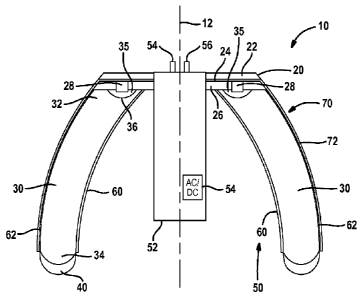
[0010] FIG. 1 is a cross-sectional view of a first embodiment of a
light
assembly according to the present disclosure.
[0011] FIG. 2A is a top view of the light tubes according to the
present
disclosure.
[0012] FIG. 2B is a top view of an alternative light pipe
configuration.
[0013] FIG. 3 is a top view of yet another alternative configuration
for
the light pipes.
2
CA 02822650 2013 06 20
WO 2012/092140
PCT/US2011/066914
[0014] FIG. 4A is a top view of a circuit board according to the
present
disclosure.
[0015] FIG. 4B is a top view of an alternate embodiment.
[0016] FIG. 4C is a top view of another alternate embodiment.
[0017] FIG. 5 is a cross-sectional view of the second embodiment of a
light assembly according to the present disclosure.
[0018] FIG. 6 is a cross-sectional view of a third embodiment of the
light assembly present disclosure.
[0019] FIG. 7 is a cross-sectional view of a fourth embodiment of a
light assembly of the present disclosure.
[0020] FIG. 8 is cross-sectional view of a light assembly according to
a
fifth embodiment of the present disclosure.
[0021] FIG. 9A is a partial cross-sectional view of a light tube.
[0022] FIG. 9B is a cross-sectional view of a light tube having a
wavelength for a light-shifting element therein.
[0023] FIG. 9C is a cross-sectional view of a light tube having a
light-
shifting element or wavelength-shifting element in a second position.
[0024] FIG. 10 is a cross-sectional view of a light assembly having a
shielded driver circuit according to the present disclosure.
[0025] FIG. 11 is a top view of light-emitting diodes or other light
sources mounted to a circuit board such as that illustrated in Fig. 10.
[0026] FIG. 12 is a cross-sectional view of a light assembly formed
having a standard Edison base.
[0027] FIG. 13 is a cross-sectional view of an alternative circuit
board
according to the present disclosure.
[0028] FIG. 14 is a top view of an alternative circuit board according
to
the present disclosure.
[0029] FIG. 15 is a cross-sectional view of an alternative view of the
conducting layer formed according to the present disclosure.
[0030] Corresponding reference numerals indicate corresponding parts
throughout the several views of the drawings.
3
CA 02822650 2013 06 20
WO 2012/092140
PCT/US2011/066914
DETAILED DESCRIPTION
[0031] The
following description is merely exemplary in nature and is
not intended to limit the present disclosure, application, or uses. For
purposes of
clarity, the same reference numbers will be used in the drawings to identify
similar elements. As used herein, the phrase "at least one of A, B, and C"
should be construed to mean a logical (A or B or C), using a non-exclusive
logical OR. It should be understood that steps within a method may be executed
in different order without altering the principles of the present disclosure.
[0032] It
should be noted that in the following figures various
components may be used interchangeably. For example, several different
embodiments of control circuit boards and light source circuit boards are
implemented. As well, various shapes of light redirection elements and heat
sinks are also disclosed. Various combinations of heat sinks, control circuit
boards, light source circuit boards, and shapes of the light assemblies may be
used. Various types of printed, stamped, oxide-coated, anodized or laser cut
electrically conductive layers and materials may also be used interchangeably
in
the various embodiments of the light assembly.
[0033] In the
following figures, a lighting assembly is illustrated having
various embodiments that include solid state light sources such as light-
emitting
diodes (LEDs) and solid state lasers with various wavelengths.
Different
numbers of light sources and different numbers of wavelengths may be used to
form a desired light output depending upon the ultimate use for the light
assembly. The light assembly provides an opto-thermal solution for a light
device and uses multiple geometries to achieve the purpose.
[0034]
Referring now to FIG. 1, a cross-section of a light assembly 10
is illustrated. Light assembly 10 includes a longitudinal axis 12. The light
assembly 10 includes a light source circuit board 20 that has a plurality of
layers
thereon. In this example, the light source circuit board includes an
insulating
layer 22 (heat conductive, not electrically conductive), an electrically and
thereby
conductive layer 24, and another electrically insulating layer 26. The light
source
circuit board 20 may be formed of conventional material such as FR4 and
metallic traces as the conducting layer 24. A multi-layer circuit board may
also
4
CA 02822650 2013 06 20
WO 2012/092140
PCT/US2011/066914
be used. The light source circuit board 20 may also be a laser-cut circuit
board
that has the circuit traces, solder pads or other conductors laser-cut
thereon.
Prior to cutting the conductors are over-molded with the insulating layer or
layers
24, 26. The circuit board 20 may have a conductive layer 24 formed of a metal
such as aluminum or stainless steel with an oxide layer or anodized layer as
the
non-electrically.
[0035] The metallic or conducting layer 24 may have a plurality of
light
sources 28 disposed thereon. The light sources 28 are solid state light
sources
such as lasers or light-emitting diodes. The lasers may be light-emitting
diode-
based. Thus, the term light-emitting diode can refer to both a laser and
conventional light-emitting diode. The conducting layer 22 may have different
sections that have various polarities so that a positive and negative
potential
difference may be generated to illuminate the light-emitting diodes. The
circuit
board 20 may have various shapes including a round shape. The circuit board
20 may have the light-emitting diodes or other light sources 28 disposed in a
ring
around the axis 12.
[0036] Each light-emitting diode 28 may have a light pipe 30
associated therewith. The light pipes 30 are elongated and extend in a
direction
generally axially from the light sources 28. In the present embodiment, the
light
pipes 30 also extend in a radially outward direction from the longitudinal
axis of
symmetry as well. The light pipes 30 in this embodiment are curved. Each light
pipe 30 has a first end 32 adjacent to the light source 28 and a second end 34
opposite the light source 28. The first end 32 may include a cavity 35 and
collimating optic 36 to collimate the light from the light source 28 into the
light
pipe 30. The cavity 35 encloses the light source 28. Of course, more than one
light source may be enclosed within the cavity. One example of a suitable
collimating optic 36 is a Fresnel lens. As will be further described below,
total
internal reflection or near total internal reflection may be used to reflect
the light
down the light pipe and out the second end 34.
[0037] The second end 34 may have a beam-forming optic 40
disposed thereon. The beam-forming optic 40 may be integrally formed with the
second end 34 of the light pipe 30. A separate component may also house the
CA 02822650 2013 06 20
WO 2012/092140
PCT/US2011/066914
beam-forming optic or optics. The beam-forming optic 40 may have various
shapes to direct the light in a desired direction or pattern. Narrow beam-
forming
with little divergence may be desirable. Also, wide-spreading flood-type beam
divergence may also be desired. The type of beam divergence or beam pattern
depends upon the specific use for the light. Thus, various beam-forming optics
may be used.
[0038] The plurality of light pipes 30 may be disposed in a circular
pattern corresponding to the ring of the light sources 28. The light pipes 30
may
form a cavity 50 therebetween. That is, the cavity 50 may be formed between
opposite light pipes 30 to form a void therebetween. The cavity is within an
inner
surface of the light assembly. The cavity 50 is the volume between the light
pipes 30.
[0039] The cavity 50 may have a driver circuit board 52 disposed
therein. The driver circuit board 52 may be electrically and mechanically
coupled
to the light source circuit board 20. The driver circuit board 52 may have
pins 54
and 56 extending therefrom. The pins 54 and 56 may be used to power the
driver circuit board 52. Electrical connections between the driver circuit
board
and the circuit board 20 may also be formed so that the light sources 28 are
powered thereby. The driver circuit board may include an AC to DC circuit 54
for
powering the light sources 28. Of course, other circuits may be included such
as
dimmer circuits, timer circuits and sensor circuits.
[0040] The light pipes 30 may also include a coating 60, 62 thereon.
The coating 60, 62 may be applied to the outer surface of the light pipe 30 to
allow the light therein to internally reflect more efficiently. The coating
60, 62
may be a reflective coating. The coating 60, 62 may also be an energy-
conversion (wavelength-converting) coating applied thereto. The coating 60, 62
allows the wavelength of the light travelling down the light pipe to convert
from
one wavelength to another wavelength. The amount of conversion may be
regulated depending upon the type of coating. The coating 60, 62 may be a
painted material or a polymer-type material applied to the outer surface of
the
light pipe. The coatings and wavelength-converting material are described
further in Figs 9A-9C.
6
CA 02822650 2013 06 20
WO 2012/092140
PCT/US2011/066914
[0041] The conductive layer 24 of the circuit board 20 may also extend
outward from the circuit board 20 and form a heat sink 70 adjacent to the
light
pipes 70 on an outer surface of the light assembly 10. The heat sink 70 may be
formed fingers of the same material as the conducting layer 24. As is
illustrated,
the conducting layer 24 extends into the heat sink 70. However, different
structures may be provided for the conducting layer 24 and the heat sink 70
that
are coupled together during manufacture. The heat sink 70 draws heat from the
light sources 28 in a radial direction and in an axial direction away from the
light
sources 28. The heat sink 70 may be referred to as a plurality of thermal
vanes
72.
[0042] Referring now to FIG. 2A, a top view of the plurality of light
pipes 30 is illustrated. As is shown, a plurality of light pipes 30 is placed
adjacent to each other in a circular pattern and is individually formed. The
light
pipes 30 have the beam-forming optics on the end thereof that is opposite the
light sources 28. The light pipes 30 are formed around the cavity 50 which
encloses the driver circuit board 52.
[0043] Each adjacent light pipe 30, in this example, has a thermal
vane
72 therebetween. The thermal vane 72, as described above, may be formed of
heat-conductive material that is thermally coupled to the light source 28 so
that
heat from the light source is drawn through the thermal vanes 72 into the
atmosphere.
[0044] The light pipes 30 in Fig. 2A are in cross-sectional shape. In
this example, the light pipes 30 are comparable to curved or bent cylinders.
The
light pipes 30 illustrated may have a shape comparable to an MR-type light.
Straight or angled light pipes are also possible.
[0045] Referring now to FIG. 2B, an alternate embodiment for a light
pipe 30' is illustrated. In this example, the light pipes 30' have a square
cross-
sectional area. The thermal vanes 72 that form the heat sink are placed
adjacent to two light pipes 30'. The light pipes may have various types of
cross-
sectional areas not illustrated in Figs. 2A and 2B including irregular shapes,
triangular shapes, octagonal shapes, hexagonal shapes and other quadrilateral
cylindrical solids.
7
CA 02822650 2013 06 20
WO 2012/092140
PCT/US2011/066914
[0046] Referring now to FIG. 3, an alternative embodiment to that set
forth in Figs. 1 and 2A is set forth. In this embodiment, all of the light
pipes 30"
are molded as a unitary structure. In the unitary structure adjacent light
pipes
are coupled together. The unitary structure of the light pipes 30" may in
integrally molded to include both the light pipes 30", the beam-forming optics
40"
and the collimating optics 36. By providing the unitary structure, the
assembly of
the light assembly may be more easily facilitated. The inner walls and outer
walls of the light pipes 30" (relative to the cavity 50) may also include
coatings
60 and 62 as illustrated in Fig. 1. However, in this embodiment, the coating
is
coated across the surface of all of the light pipes 30".
[0047] Referring now to FIG. 4A, one embodiment of a circuit board 20
is illustrated. The circuit board 20 includes the plurality of light sources
28
thereon. The circuit board 20 includes a radial outward thermal path 110. An
opening 114 may be provided through the circuit board 20 to receive the driver
circuit board 52. The light sources 28 illustrated in Fig. 4 may have more
electrical components for driving the light sources incorporated onto the
circuit
board 20. For example, solder pads 410 may be disposed on the circuit board
20 in pairs to mount the respective cathodes and anodes of the light-emitting
diodes 28 thereon. Thermal vias 116 may be provided throughout the circuit
board 20 to allow a thermal path to the thermal vanes 72 of the heat sink 70
as
illustrated in Fig. 1. As is illustrated, the thermal vias 116 are generally
laid out
in a triangular or pie-piece arrangement but do not interfere with the thermal
paths 110. Thermal vias 116 may also be placed directly under the light
sources.
[0048] The circuit board 20 may be made out of various materials to
form a thermally-conductive substrate. The solder pads of the light sources 28
may be connected to radial-oriented copper sectors or circular conductive
elements that are over-molded into a plastic base to conduct heat away from
the
light sources. By removing the heat from the area of the light sources, the
lifetime of the light assembly 10 may be extended as compared to non-heat
removing assemblies. The circuit board 20 may be formed from two-sided FR4
material, heat sink material, or the like. If the board material is
electrically
8
CA 02822650 2013 06 20
WO 2012/092140
PCT/US2011/066914
conductive, the electrical traces may be formed on an electrically non-
conductive
layer that is formed on the electrically conductive surface of the circuit
board.
The electrically non-conductive layers may be formed of thermally conductive
material such as thermally conductive plastic.
[0049] Electrical connections 118, 120 may be formed between the
circuit board 20 and the drive circuit board 52 to provide power from the
driver
circuit board 52 to the light sources 28.
[0050] Referring now to FIG. 4B, an alternative embodiment of the
circuit board 20' is illustrated. The circuit board 20' may include a
plurality of
circuit trace sectors 130 and 132 that are coupled to alternate voltage
sources to
power the light sources 28. The sectors 130, 132 are separated by a non-
conductive gap 134. The light sources 28 may be electrically coupled to
alternate sectors 130, 132. The light sources 28 may be soldered or otherwise
electrically mounted to the two sectors 130, 132.
[0051] Each sector 130, 132 may be disposed on a non-conductive
circuit board 20'. As mentioned above, the circuit board 20' may also be
formed
of a heat sink material. Should the heat sink material be electrically
conductive,
a non-conductive pad or layer may be placed between the sectors 130, 132 and
the circuit board 20'.
[0052] Referring now to FIG. 4C, another embodiment of a circuit
board 20" is illustrated. The circuit board 20" includes the light sources 28
that
are spaced apart by circuit traces 140 and 142. The circuit traces 140 and 142
may have different voltages used for powering or activating the light sources
32.
The circuit traces 140, 142 may be printed on a substrate. Electrical
connections
may be made from the driver control circuit board.
[0053] Referring now to FIG. 5, another embodiment of a light
assembly 10' is illustrated. In this embodiment, the structure is nearly
identical to
that set forth in Fig. 1. In this embodiment, however, the light pipes 30' are
curved in the opposite direction. The curve of the light pipes 30' compared to
Fig. 1 stays closer to the light forces and the longitudinal axis 12 and then
curves
away from the longitudinal axis at the second end 34.
9
CA 02822650 2013 06 20
WO 2012/092140
PCT/US2011/066914
[0054] The remaining components are the same and thus are labeled
with the same reference numerals.
[0055] Referring now to FIG. 6, a similar embodiment of the light
assembly 10' to that illustrated in Fig. 1 is set forth. In this embodiment,
the light
pipes 30 have a cover portion 610 thereon. The cover portion 610 covers the
cavity 50 and is used for light redistribution. The cover portion 610 may also
have a reflective coating 612 on the back side thereof. The reflective coating
helps reflect light outward from the light assembly 10". A reflective coating
614
may also be disposed on an angled surface 616. The angled surface 616
reflects or redirects light toward the angled surface 618 which in turn
reflects
light outward from the light surface as illustrated by the arrow 620. The
light
travelling up the light tube from the light source 28 reflects from the first
angular
surface 16 and from the second angular surface 18 to reflect outward from a
light-emitting surface 630 of the cover 610. The light-emitting surface 630
may
also have light or beam-forming elements 631 disposed thereon to scatter the
light or redirect the light as desired. The cover 610 helps redistribute the
light
across the light distribution surface 630.
[0056] Referring now to Fig. 7, another embodiment of a light pipe 30"
is set forth. The light pipes 30" extend perpendicularly from the surface of
the
circuit board 20'. In this embodiment, a cover 710 is also used. The cover 710
has a spherical outer surface 712. A coupler 714 is used for coupling the
light
pipe 30' to the cover 710. The coupler 714 allows light to pass from the light
pipe 30" into the cover 710. The cover 710 also has a curved inner surface
716.
Light from the light pipe 30" enters the cover 710 through the coupler 714.
The
light is partially emitted as illustrated by arrow 720 and is partially
reflected as
illustrated by arrow 722. The light reflected from the surface 712 reflects
from
the surface 716 and outward from the cover 720. In this manner, the light is
more distributed across the surface of the cover 710.
[0057] Referring now to FIG. 8, a similar embodiment to that
illustrated
in Fig. 7 is set forth. However, in this embodiment, a wavelength-shifting
element or light-shifting element 810 is illustrated. In this embodiment of
the
light assembly 101, the light from the light source 28 is directed through a
light-
CA 02822650 2013 06 20
WO 2012/092140
PCT/US2011/066914
shifting element 810. The light-shifting element 810 may also be referred to
as a
wavelength-shifting element. The light source 28 may generate light at a first
wavelength and the wavelength-shifting 18 changes the wavelength to a second
wavelength. One example of wavelength-shifting is blue light from the LED
shifted to white light. The light from the light sources may pass directly
through
the light-shifting or wavelength-shifting element 810 to perform the
wavelength-
shifting. In this embodiment, the wavelength-shifting element 810 is disposed
adjacent to the light source 28 within a cavity 820 that forms the collimating
element. Thus, the light traveling down the light pipe is light-shifted light
in Fig.
8.
[0058]
Referring now to FIG. 9A, the light source 28 is illustrated
adjacent to a light pipe 30. The light pipe 30 in Figs. 9A-9C is illustrated
as a
cylindrical light pipe. However, the light pipe may represent any one of the
above-illustrated light pipes such as the curved light pipe shown in Figs. 1,
5 and
6. Also, various cross-sections of light pipes may be used. In this
embodiment,
a wavelength-shifting element 910 is disposed adjacent to the outer surface of
the light pipe 30. The wavelength-shifting element 910 shifts the wavelength
of
the light incident upon the outer surface so that as the light travels down
the light
tube 30, the light travels into the light-shifting element. In
response, the
wavelength of the light is shifted to a second wavelength different than the
first
wavelength. The wavelength output may be tailored for the application, such as
home use, agricultural use and inspection system use. Various types of films
and coatings may be used. In addition to the wavelength-shifting element 910,
a
coating 912 may be disposed on the outside of the wavelength-shifting element
910.
[0059]
Referring now to FIG. 9B, a wavelength-shifting element 920 is
disposed within the light pipe 30. The wavelength-shifting element 920 may be
integrally molded within the light tube and extend across the entire diameter
of
the light tube. As the light passes down and through the light pipe 30, the
light is
shifted to a different wavelength. The wavelength-shifting element 920 may not
provide 100% efficiency at a first pass therethrough and thus light will have
its
wavelength shifted as it passes through the wavelength-shifting element 920.
In
11
CA 02822650 2013 06 20
WO 2012/092140
PCT/US2011/066914
this embodiment, the wavelength-shifting element is located near or at the
center
of the light pipe 30.
[0060] A
coating 922 may also be formed on the outside of the light
pipe 30 to help reflect light within the light pipe and keep the light within
the light
pipe.
[0061]
Referring now to FIG. 9C, another embodiment of the light pipe
30 is illustrated that includes a light-shifting element 930. The light-
shifting
element 930 is disposed adjacent to one surface of the light pipe 30. As light
travels down the light pipe 30, light travels through the wavelength-shifting
element 930 and is shifted in wavelength to a second wavelength. As discussed
above, the wavelength-shifting element 930 may not be 100% efficient and thus
more light wavelengths are shifted as the reflected light passes through the
wavelength-shifting element 930.
[0062] In this
embodiment, a coating 932 may also be disposed on the
outer surface of the light pipe 30.
[0063]
Referring now to FIG. 10, another embodiment of a circuit
board 1010 is set forth. In this embodiment, a conductive layer 1012 has a
first
insulating layer 1014 and a second insulating layer 1016 thereon. A light
source
1018 is mounted to the conducting layer 2012. In this embodiment, the
conducting layer extends to form a cavity 1030 that is used to receive the
driver
circuit board 52. The
driver circuit board 52 may have high frequency
components thereon. By
providing a conductive circuit board 1030, an
enclosure 1040 may be formed around the circuit board 52 to shield any RF
interference generated by the high-frequency components of the driver circuit
board 52. The enclosure 1040 illustrated has a first sidewall 1042 and a top
portion 1044. The sidewall may extend around the driver circuit board 52 and
the top wall 1044 may extend over the driver circuit board 52. To further
promote RF isolation, the enclosure 1040 may be electrically coupled to ground
potential. However, the enclosure 1040 may also be electrically isolated.
[0064] In
forming the circuit board 1010, the metal portions may be
stamped to provide the desired circuit traces. The metal may then be over-
molded with the insulating layers 1012 and 1014. After molding, further
12
CA 02822650 2013 06 20
WO 2012/092140
PCT/US2011/066914
refinements of the circuit traces may be formed by laser cutting or other
types of
machining if desired.
[0065] Referring now to FIG. 11, a partial top cross-sectional view of
the enclosure 1040 of Fig. 10 is set forth. In this example, a plurality of
light
sources is electrically coupled to two different polarity segments 1110 and
1120.
Thermal vias 1122 are also disposed on the circuit board. In this embodiment,
a
gap 1140 is provided between each of the adjacent polarity portions 1110, 1120
and the enclosure 1040. The gap 1140 is non-conducting and therefore the
different polarities used to rate the light sources 1018 is provided.
[0066] Referring now to FIG. 12, the light assembly may also include a
standard Edison base 1210. The standard Edison base 1210 is one example of
an alternative base used for a light bulb. An Edison base 2010 has a first
polarity portion 1212 and a second polarity portion 1214. The first polarity
portion 1212 is coupled to one lead 1216 of the circuit board 52. The second
polarity 1214 is coupled to a second lead 1218 coupled to the circuit board
52.
[0067] The base 1210 may be formed of a material that is conductive
in different regions and separated by a non-conductive area. Of course,
different
styles and shapes of bases for different applications may be provided.
[0068] Referring now to FIG. 13, an alternative cross-sectional view
of
a light circuit board with a light source thereon is set forth. In this
example, a
non-electrically conducting layer 1310 is illustrated. A conductive layer 1312
has
an oxide layer 1314 associated therewith. The oxide layer 1314 is a non-
electrically, but thermally, conductive layer. The conducting layer 1312 may
be
stainless steel, aluminum or another type of electrically conducting metal.
The
non-conducting layer 1314 may be an anodized layer or an oxide layer formed
on the metal. On top of the non-conducting layer 1314 circuit traces 1316 may
be disposed thereon. An example of a suitable circuit trace 1316 may be a
printed conductive ink. A light-emitting diode 1320 may be electrically
coupled to
the circuit trace 1316. In this example, the conductive layer 1312 may be
stamped to form the cavity for receiving the circuit boards 1330 therein. Both
the
conductive layer and the non-conductive oxide or anodized layer 1314 may also
be stamped and formed in the same manner. The circuit traces 1316 may be
13
CA 02822650 2013 06 20
WO 2012/092140
PCT/US2011/066914
applied to the non-conducting layer 1314 and the light-emitting diodes 1320
electrically coupled thereto by reflow soldering or the like. The whole
assembly
may then be over-molded with the non-conductive layer 1310. Thereafter, lasers
or other cutting techniques may be used to electrically isolate or separate
the
solid conducting layers 1312 to form different polarities. One pattern for
cutting
conductive traces is illustrated in Fig. 14 below.
[0069] Referring now to FIG. 14, a top view of the circuit board
illustrated in Fig. 13 is set forth. In this example, gaps or cuts 1410 are
provided
through the conductive layer 1312 so that different regions are isolated on
the
circuit board. In the cut areas 1410, the polarities of adjacent components
are
separated. Pluses and minuses are disposed on the surface to illustrate a
cathode and anode of the light-emitting diode may be disposed thereon on each
conductive surface. A light source such as the light-emitting diode 1414 is
illustrated straddling a cut 1410. Adjacent light-emitting diodes 1410 may
thus
be connected in series because the cathode of one light-emitting diode is
coupled to the anode of an adjacent light-emitting diode. Various other
interconnections may also be desired to be formed. Another cut 1420 is an
annular cut to separate a positive potential and negative potential (ground)
regions. A positive potential circuit trace 1422 and a negative potential
circuit
trace 1424 are set forth. When interconnections are desired from the solder
pad
regions 1430, wire-bonding techniques may be used for the interconnections.
Essentially the two different polarity traces are annular.
[0070] Referring now to FIG. 15, the same techniques described
above may also be used for an inverted-type system. In this system, a base
1510 may be interconnected with a driver circuit board 1512. The driver
circuit
board 1512 may be disposed in a cavity 1514 that is provided the conductive
layer 1520. The LEDs 1522 may be mounted directly on the conductive layer or
on solder pads disposed on a second conductive layer spaced apart from the
conductive layer 1524.
[0071] Leads 1530 and 1532 may interconnect the circuit board to the
base 1510 and provide different polarities for operating the driver circuit
board
1512 and ultimately the light-emitting diodes 1522 or other types of light
sources.
14
CA 02822650 2013 06 20
WO 2012/092140
PCT/US2011/066914
[0072] The
foregoing description of the embodiments has been
provided for purposes of illustration and description. It is not intended to
be
exhaustive or to limit the invention.
Individual elements or features of a
particular embodiment are generally not limited to that particular embodiment,
but, where applicable, are interchangeable and can be used in a selected
embodiment, even if not specifically shown or described. The same may also be
varied in many ways. Such variations are not to be regarded as a departure
from
the invention, and all such modifications are intended to be included within
the
scope of the invention.