Note: Descriptions are shown in the official language in which they were submitted.
CA 02822685 2016-06-03
WO 2012/088610 PCTICA20111050814
LOW LOSS DIRECTIONAL COUPLING BETWEEN HIGHLY DISSIMILAR OPTICAL
WAVEGUIDES FOR HIGH REFRACTIVE INDEX INTEGRATED PHOTONIC
CIRCUITS
Technical Field
The present invention relates to a method of achieving high efficiency optical
signal
coupling between low refractive index waveguides and high refractive index
waveguides.
Background
In the field of microelectronics there is a push to integrate photonics and
microelectronics in order to improve the performance of current electronic
systems. The
possibility of permitting optical communication between integrated chips via
an optical
bus would have a major impact on the performance of electronic systems.
Research in
this field is very active, however proposed solutions until now have been
unsuitable and
are difficult to realize in practice.
Efficient coupling of highly dissimilar refractive index waveguides has always
been a
problem in many applications.
For example, optical fiber waveguides have been employed to convey optical
signals.
Optical fibers include an optical fiber core within a cladding. Optical fiber
waveguide to
optical fiber waveguide butt-coupling requires high precision alignment.
Semiconductor
waveguides typically have smaller geometries and higher refractive indices
compared to
1
CA 02822685 2013-06-21
WO 2012/088610 PCT/CA2011/050814
optical fiber geometries and refractive indices. The geometry mismatch stems
from
mode confinement requirements, the higher refractive index of semiconductor
waveguides demands smaller geometries. Butt-coupling between optical fibers
and
semiconductor waveguides require extremely high precision alignment and
suffers from
high coupling losses due to refractive index mismatches.
In the field of integrated opto-electronic devices, light (optical signal)
coupling between
"on chip" waveguides and external waveguides is conventionally done using butt-
coupling between an external fiber core and the core of an on-chip waveguide
or its
optical interconnect device. On-chip opto-electronic devices include vertical
cavity
lasers, horizontal cavity lasers, photodiodes and phototransistors. On-chip
optical
devices include splitters and couplers.
What prevents major progress in the field is an intrinsic property of silicon,
the principal
semiconductor utilized in microelectronics, which has a high index of
refraction (about
3.5) compared to that of optical fibers (about 1.47). The index of refraction
of
germanium, another important semiconductor utilized in microelectronics is
about 4.
This prevents efficient injection of an optical signal from one material to
the other in two
different ways: First, the large index of refraction difference between them
causes the
creation of reflections at the injection interface. Second, the required
geometries of an
optical fiber and of a waveguide of a high index of refraction for single mode
optical
signal propagation are radically different. Both of these factors reduce the
ability to
couple (transfer) optical signals with acceptable losses.
A similar problem exists in the field of biosensors between different
materials than those
employed in microelectronics however with comparable differences in refractive
indices.
While employing such hybrid integration technologies, an external optical
signal may not
be injected into a chip. However, the coupling experiences the same difficulty
in
injecting the signal into a layer of a high index of refraction.
On-chip waveguides typically comprise waveguides made of silicon or germanium
having indices of refraction of about 3 to 4, which are much higher than the
index of
refraction for an optical fiber core (dielectric waveguide). For single mode
fibers, core-
2
CA 02822685 2013-06-21
WO 2012/088610 PCT/CA2011/050814
to-core butt-coupling requires high precision alignment and superior
mechanical
stability, both of which add significant cost to providing such optical
connections. Not
only must alignment be provided, but also a good match in the waveguide
properties is
required to ensure that the desired modes are coupled between waveguides. In
many
applications, optical coupling is such a challenge that designs resort to opto-
electronic
conversion of signals to use electrical coupling between on-chip and off-chip
optical
signals.
In coupling optical signals to and from on-chip waveguides or opto-electronic
devices,
conventional techniques involve mounting optical fibers with precision to rest
horizontally on the integrated circuit with a prism reflector being used to
redirect the light
vertically into a waveguide or optical device on the integrated circuit.
Conventional
techniques also include precision mounting of the fiber vertically on the
integrated
circuit. These techniques are costly to implement due to difficulties in
reproducing and
maintaining alignment precision.
Recently evanescent field waveguide coupling has been proposed for optical
signal
coupling between an optical fiber waveguide and a semiconductor waveguide.
A theoretical treatise was provided by Borges, B.-H. V. and Herczfeld, P. R.,
entitled
"Coupling from a Single Mode Fiber to a III-V Thin-Film Waveguide via
Monolithic
Integration of a Polymeric Optical Waveguide", Journal of the Franklin
Institute, vol.
335B, no 1, p. 89-96, 1998. Borges describes the results of theoretical
modeling of
evanescent field waveguide coupling between a polymer waveguide and a sheet
waveguide of unlimited extent as well results of modeling evanescent field
waveguide
coupling between a polymer waveguide and a sheet waveguide of unlimited extent
having a step discontinuity. While the mathematical modeling seems to suggest
promising coupling efficiencies, the presented results cannot be employed in
practice as
usable waveguides have limited widths and therefore the presented results
cannot be
reproduced in practical implementations. Experimental trials attempting to
duplicate
Borges account only for a small fraction of the promised results. An effective
refractive
index variation is described by Borges, at the bottom of page 90 thereof, to
come from
exploiting "linear and quadratic electro-optic effects, as well as plasma,
band filling, and
3
CA 02822685 2013-06-21
WO 2012/088610 PCT/CA2011/050814
band shrinkage to yield a high figure of merit for index modulation". Such
coupling
makes use of an important perturbation of the optical field at the entrance of
the chip:
The semiconductor upper cladding creates the perturbation and the optical
field first
partially couples into the upper cladding to finally transfer to the waveguide
layer. That
approach also creates a significant amount of radiative (lossy) mode coupling
and
higher order mode coupling which have not been addressed by Borges. Also, a
number
of assumptions have been demonstrated to be wrong in respect of structures
having
high refractive index differences. Furthermore, the lack of symmetry in the
Borges
approach prevents reverse optical signal (light) propagation from inside of
the chip to
the outside.
Further attempts at implementing evanescent field waveguide coupling describe
tapered
structures that slowly adapt the optical field of a first waveguide to match
the optical
field of a second waveguide. Such structures are difficult to fabricate due to
a
requirement for three-dimensional (3D) shaping during manufacture.
For example, one attempt at addressing the coupling problem provided tapered
waveguides having large geometries in high refractive index materials.
Numerous
proponents have simulated such devices, and the simulations seem to suggest
high
optical signal injection efficiencies. Such attempts include: Dai, D., He, S.
and Tsang,
H.-K. "Bilevel Mode Converter Between a Silicon Nanowire Waveguide and a
Larger
Waveguide", Journal of Lightwave Technology, vol. 24, no 6, p. 2428-33, June
2006;
and Doylend, J. K. and Knights, A. P. "Design and Simulation of an Integrated
Fiber-to-
Chip Coupler for Silicon-on-Insulator Waveguides", IEEE Journal of Selected
Topics in
Quantum Electronics, vol. 12, no 6, p. 1363-70, November 2006. While these
simulations might suggest polarization independent solutions, only a limited
number of
such devices have been manufactured given the 3D nature of the devices.
Another attempt included employing a large size waveguide coupled with a
reverse
tapered waveguide of high refractive index described by Galan, J., Sanchis,
P.,
Sanchez, G. and Marti, J., "Polarization Insensitive Low-Loss Coupling
Technique
between 501 Waveguides and High Mode Field Diameter Single-Mode Fibers",
Optics
Express, vol. 15, no 11, p. 7058-65, 2007. According to this attempt, such
geometry
4
CA 02822685 2013-06-21
WO 2012/088610 PCT/CA2011/050814
permits obtaining good injection efficiency and has little polarization
sensitivity.
However, problems arise from the requirement for manufacturing a suspended
structure
which is very fragile. Furthermore, the tapered waveguide has to have
extremely small
dimensions. Such implementations demand use of high resolution lithography at
increased costs.
A further attempt consists using prisms integrated within chips as described
by Ghiron,
M., Gothoskar, P. Montgomery, R. K., Patel, V., Pathak, S., Shastri, K. and
Yanushefski, K. A. in US patent 7,058,261 B2, entitled "Interfacing Multiple
Wavelength
Sources to Thin Optical Waveguides utilizing Evanescent Coupling" and
published June
6, 2006 and in US patent 7,020,364 B2 "Permanent Light Coupling Arrangement
and
Method for use with Thin Silicon Optical Waveguides" published March 28, 2006.
Once
again, the 3D character and the numerous fabrication steps required, relegate
such
solutions to laboratory settings rendering them unviable for practical
applications.
Yet another attempt includes employing a diffractive grating engraved directly
into the
high refractive index material as described by: Roelkens, G., Van Campenhout,
J.,
Brouckaert, J., Van Thourhout, D., Baets, R., Romeo, P. R., Regreny, P.,
Kazmierczak,
A., Seassal, C., Letartre, X., Hollinger, G., Fedeli, J. M., Di Cioccio, L.
and Lagahe-
Blanchard, C., in "III-V/Si Photonics by Die-to-Wafer Bonding", Materials
Today, vol. 10,
no 7-8, p. 36-43, July-August 2007; Taillaert, D., Van Laere, F., Ayre, M.,
Bogaerts, W.,
Van Thourhout, D., Bienstman, P. and Baets, R., in "Grating Couplers for
Coupling
Between Optical Fibers and Nanophotonic Waveguides", Japanese Journal of
Applied
Physics, vol. 45, no 8A, p. 6071-6077, 2006; and Taillaert, D. and Baets, R.,
in US
patent 7,065,272 B2 entitled "Fiber-to-waveguide coupler" published April 26,
2005.
Initial experimental results appear to show that the signal injection
efficiency is relatively
good and polarization independent. Also, the injection is totally independent
of the
"state" of the facets. Despite these advantages, the required fabrication
complexity is
high, because such implementations demand high resolution lithography and high
precision engraving techniques. Furthermore, alignment has to be controlled
very well
in order to avoid optical signal losses.
5
CA 02822685 2013-06-21
WO 2012/088610 PCT/CA2011/050814
Other attempts propose coupling schemes requiring nanofabrication, which can
also be
difficult to incorporate into CMOS chips.
There is a need in the field for increasing optical coupling efficiencies
between low
refractive index (dielectric) waveguides and high refractive index
semiconductor
waveguides.
Summary
It has been found that continuously varying the thickness and/or width of
structures to
provide prior art tapers for adiabatic energy transfer from a guiding
structure to another
requires extreme complexity. In contrast is has been discovered that employing
layer
thickness control during semiconductor fabrication provides beneficial
manufacturing
advantages.
It has been discovered that the above identified prior art shortcomings can be
addressed via a two step approach wherein:
1. Coupling an optical signal propagating in an external optical fiber into an
intermediary
waveguide having a refractive index comparable to that of the external optical
fiber, the
intermediary waveguide being waferscale manufactured employing standard
micrometer resolution photolithographic techniques providing a relatively
simple and
effective coupler.
2. Coupling the optical signal propagating in the intermediary waveguide into
a
nanometric high refractive index semiconductor waveguide. The proposed
solution
implements directional optical coupling. The coupling is preferably done from
the
fundamental mode of a first waveguide to the fundamental mode of a second
waveguide (single mode light propagation). The first waveguide can be the
lower
refractive index waveguide or the higher refractive index waveguide, depending
on the
application. The coupling scheme described is reciprocal with respect to
the
waveguides, which means that an optical signal can travel efficiently in both
wave
propagation directions, from the intermediary waveguide to the semiconductor
6
CA 02822685 2013-06-21
WO 2012/088610 PCT/CA2011/050814
waveguide or from the semiconductor waveguide to the intermediary waveguide.
Directional coupling arises when an output waveguide is located in the
proximity of an
input waveguide in which an optical signal propagates. If the evanescent field
extending from the propagating mode of the input waveguide conveying the
optical
signal enters the core of the neighboring waveguide, such coupling usually
happens
through tunneling-like phenomena. When the two waveguides are similar in terms
of
wave vector amplitude and direction, an efficient energy transfer can take
place.
Embodiments according to the proposed solution require only little in terms of
fabrication complexity. Waveguide alignment is provided by photolithography of
semiconductor structures having a high refractive index. Such alignment is
relatively
simple to produce and is enabled by a precise control of layer thicknesses for
the
interface between the nanometric high refractive index waveguide and the
intermediary
low refractive index waveguide. Such optical signal coupling into a waveguide
having a
nanometric thickness can be realized efficiently.
It has also been discovered that the dimensions of the waveguides can be
easily tuned
in many cases to allow efficient (optical signal) light coupling between very
dissimilar
waveguides.
It has further been discovered that the proposed solution is compatible with
standard
CMOS fabrication processes and therefore has wide applicability. The proposed
solution permits coupling of external optical signals (e.g. from an optical
fiber) (e.g. a
hybrid optical source) into a photonic circuit inside a microchip, photonic
circuit which is
fabricated from high refractive index materials. The reverse is equally
possible.
In accordance with an aspect of the invention there is provided an integrated
circuit
physical optical Input/Output (I/O) interface for coupling at least one mode
of an optical
signal between a waveguide external to the integrated circuit and a high
refractive index
waveguide internal to the integrated circuit, the physical optical interface
comprising: an
I/O waveguide conveying an external optical signal near the integrated circuit
along an
external signal path, said I/O waveguide having a first refractive index; and
a high
7
CA 02822685 2013-06-21
WO 2012/088610 PCT/CA2011/050814
refractive index coupler waveguide forming part of the integrated circuit and
conveying
an internal optical signal along an internal signal path, said high refractive
index
waveguide having a second bulk refractive index substantially dissimilar from
said first
refractive index, said high refractive index waveguide having at least a
portion with a
thickness configured to exhibit an effective refractive index substantially
matching said
first refractive index of said I/0 waveguide, said high refractive index
waveguide and
said I/O waveguide being arranged substantially parallel and in proximity with
an
overlap therebetween to permit tunnel coupling of said at least one mode of
said optical
signal between said internal signal path and said external signal path.
In accordance with another aspect of the invention there is provided an
optical
interconnect comprising at least one integrated circuit physical optical
Input/Output (I/O)
interface for coupling at least one mode of an optical signal between a
waveguide
external to the integrated circuit and a waveguide internal to the integrated
circuit, the
physical optical interface comprising: an I/O waveguide conveying an external
optical
signal near the integrated circuit along an external signal path, said I/O
waveguide
having a first refractive index; and a coupler waveguide forming part of the
integrated
circuit and conveying an internal optical signal along an internal signal
path, said
internal waveguide having a second bulk refractive index substantially
dissimilar from
said first refractive index, said semiconductor waveguide having at least a
portion with a
thickness configured to exhibit an effective refractive index substantially
matching said
first refractive index of said I/O waveguide, said internal waveguide and said
I/O
waveguide being arranged substantially parallel and in proximity with an
overlap
therebetween to permit tunnel coupling of said at least one mode of said
optical signal
between said internal signal path and said external signal path.
In accordance with a further aspect of the invention there is provided a
process for
manufacturing a low loss coupler, the process comprising patterning an
oxidation mask
on top of a device layer; and thinning the device layer down to a thickness
comprised
between 20nm and 200nm.
In accordance with a further aspect of the invention there is provided a
process for
manufacturing a low loss coupler, the process comprising fabricating a shadow
mask on
8
CA 02822685 2013-06-21
WO 2012/088610 PCT/CA2011/050814
top of a high refractive index layer; and plasma etching resulting in
vertically tapered
structures.
In accordance with a further aspect of the invention there is provided a
process for
manufacturing a low loss coupler, the process comprising: fabricating a
shadowing
mask on top of a high refractive index layer, said shadowing mask having an
overhang;
depositing an etching mask material over said overhanging shadowing mask, said
etching mask material forming a taper region under the overhang; removing said
overhanging shadowing mask; and plasma etching both said high refractive index
layer
and etching mask vertically, said taper region causing said high refractive
index layer to
be etched non-uniformly forming a tapered structure therein as said tapered
etching
mask retreats across said tapered region.
In accordance with a further aspect of the invention there is provided a
process for
manufacturing a low loss coupler, the process comprising employing a shadowing
mask
during deposition.
In accordance with yet another aspect of the invention there is provided a
optical signal
coupler for coupling at least one mode of an optical signal between at least
one
Input/Output (I/O) waveguide conveying an external optical signal along an
external
signal path and a corresponding high refractive index waveguide forming part
of an
integrated circuit, each said high refractive index waveguide conveying an
internal
optical signal along an internal signal path, said coupler comprising: each of
said at
least one I/O waveguide having a first bulk refractive index, each said
corresponding
high refractive index waveguide having a second bulk refractive index
substantially
dissimilar from said first refractive index; at least one alignment structure
for positioning
said at least one I/O waveguide with respect to said corresponding high
refractive index
waveguide substantially in parallel, in proximity and with an overlap
therebetween to
permit tunnel coupling of said at least one mode of said optical signal
between said
external signal path and said internal signal path, said high refractive index
waveguide
having at least a portion with a thickness configured to exhibit an effective
refractive
index substantially matching said first refractive index of said I/O
waveguide.
9
CA 02822685 2013-06-21
WO 2012/088610 PCT/CA2011/050814
Brief Description of the Drawings
The invention will be better understood by way of the following detailed
description of
embodiments of the invention with reference to the appended drawings, in
which:
Figure 1 is a schematic side view diagram illustrating aspects of the proposed
solution;
Figure 2a is a plot illustrating, in accordance with the proposed solution, a
variation of
an effective refractive index of a high refractive index waveguide with
waveguide layer
thickness for a given waveguide width, wherein the width is assumed to be very
large
compared to the thickness;
Figure 2b is a plot illustrating, in accordance with the proposed solution,
variations of
the effective refractive index of a silicon waveguide for both polarization
states, for a
waveguide width of 4.2 microns and a free space wavelength of 1.55pm;
Figure 2c is a plot illustrating, in accordance with the proposed solution, a
variation of a
coupling efficiency from a low refractive index material waveguide having a
core index
of 1.57 to a silicon waveguide as a function of effective refractive index
detuning,
wherein a detuning value of 0 corresponds to a perfectly matched structure;
Figure 2d is a plot illustrating, in accordance with the proposed solution, a
variation of
the coupling efficiency from a low refractive index material waveguide having
a core
index of 1.57 to a silicon waveguide as a function of the width of the silicon
waveguide;
Figure 2e is a plot illustrating, in accordance with the proposed solution, a
variation of
the coupling efficiency from a low refractive index material waveguide having
a core
index of 1.57 to a silicon waveguide as a function of misalignment between the
centers
of the waveguides;
Figure 3a is a schematic diagram illustrating, in accordance with the proposed
solution,
a side view of an embodiment of the proposed solution wherein the first
waveguide is an
optical fiber from which some cladding has been removed in order to allow
bringing the
CA 02822685 2013-06-21
WO 2012/088610 PCT/CA2011/050814
core close enough to the high refractive index waveguide, the exposed optical
core
representing an intermediary waveguide;
Figure 3b is another schematic diagram illustrating a top view of the
embodiment
illustrated in Figure 3a;
Figure 3c is yet another schematic diagram illustrating a cross-sectional view
perpendicular to a circular optical fiber core axis;
Figure 4a is a schematic diagram illustrating a side view of another
embodiment of the
proposed solution wherein the first waveguide is an intermediary waveguide to
which
light is butt-coupled from an optical fiber of a similar refractive index;
Figure 4b is another schematic diagram illustrating a top view of the
embodiment
illustrated in Figure 4a;
Figure 4c is a further schematic diagram illustrating a cross-sectional view
perpendicular to the optical fiber core axis with a circular optical fiber
shown in dotted
lines to improve clarity. A v-groove structure is employed to provide improved
(optimal)
alignment;
Figure 4d is yet another schematic diagram illustrating a front view of the
embodiment,
showing the optical fiber in a V-groove alignment structure;
Figure 5a is a schematic diagram illustrating, in accordance with a further
embodiment
of the proposed solution, a top view of packaging aspects of bringing an
optical bus into
a package for connection to a semiconductor chip;
Figure 5b is another schematic diagram illustrating a cross-sectional view of
the
embodiment illustrated in Figure 5a along the optical bus/waveguides;
Figure 5c is yet another schematic diagram illustrating another cross-
sectional view of
the embodiment illustrated in Figure 5a perpendicular to the waveguides;
Figure 6a is a schematic diagram illustrating, in accordance with a further
embodiment
of the proposed solution, a side view of an implementation wherein the high
refractive
11
CA 02822685 2013-06-21
WO 2012/088610 PCT/CA2011/050814
index material waveguide is fabricated on top of the (intermediary) low
refractive index
waveguide layer;
Figure 6b is another schematic diagram illustrating a top view of the
embodiment of
Figure 6a;
Figure 6c is yet another schematic diagram illustrating a cross-sectional view
of the
embodiment of Figure 6a;
Figure 7a is schematic diagram illustrating, in accordance with a further
embodiment of
the proposed solution, a top view of a structure controlling coupling length
by patterning
the intermediary waveguide with an s-bend;
Figure 7b is schematic diagram illustrating, in accordance with a further
embodiment of
the proposed solution, a top view of a structure controlling coupling length
by patterning
the high refractive index waveguide with an s-bend;
Figure 8a is a schematic diagram illustrating, in accordance with a further
embodiment
of the proposed solution, a top view of a single input being distributed over
many
outputs, wherein a intermediary waveguide is patterned with s-bends to control
each
coupling length;
Figure 8b is another schematic diagram illustrating, in accordance with a
further
embodiment of the proposed solution, a top view of a single input being
distributed over
many outputs, wherein high refractive index waveguides are patterned with s-
bends to
control each coupling length;
Figure 8c is yet another schematic diagram illustrating, in accordance with a
further
embodiment of the proposed solution, a top view of a single input being
distributed over
many outputs, wherein a demultiplexing structure is employed to distribute an
optical
signal over many outputs;
Figure 9a is a schematic diagram illustrating, in accordance with a further
embodiment
of the proposed solution, a top view of multiple inputs being mixed together
into a single
12
CA 02822685 2013-06-21
WO 2012/088610 PCT/CA2011/050814
output, wherein a high refractive index waveguide is patterned to form
multiple
directional coupler sections;
Figure 9b is another schematic diagram illustrating, in accordance with a
further
embodiment of the proposed solution, a top view of multiple inputs being mixed
together
into a single output, wherein multiple intermediary waveguides are patterned
to form
multiple directional coupler sections;
Figure 9c is yet another schematic diagram illustrating, in accordance with a
further
embodiment of the proposed solution, a top view of multiple inputs being mixed
together
into a single output, wherein the high refractive index waveguide includes a
multiplexing
structure to mix multiple input optical signals into a single output;
Figure 10a is a schematic diagram illustrating, in accordance with a further
embodiment
of the proposed solution, a top view of a directional coupler structure where
an input
optical signal is coupled from a single intermediary waveguide to two high
refractive
index waveguides simultaneously, the two high refractive index waveguides
being
located side by side addressing a polarization dependency of the proposed
solution;
Figure 10b is a schematic diagram illustrating a cross-sectional view of the
directional
coupler structure of Figure 10a;
Figure 11 a is a schematic diagram illustrating, in accordance with a further
embodiment
of the proposed solution, a top view of a directional coupler structure where
an input
optical signal is coupled from a single intermediary waveguide to two high
refractive
index waveguides simultaneously, the two high refractive index waveguides
being
located one above and one below of the intermediary waveguide addressing a
polarization dependency of the proposed solution;
Figure 11 b is a schematic diagram illustrating a cross-sectional view of the
directional
coupler structure of Figure 11a;
Figure 12 is a schematic diagram illustrating, in accordance with a further
embodiment
of the proposed solution, a side view of a structure where the high refractive
index
waveguide includes multiple sections of different thicknesses within the
coupling region
13
CA 02822685 2013-06-21
WO 2012/088610 PCT/CA2011/050814
to optimize both TE and TM directional coupling into a single high refractive
index
waveguide;
Figure 13a is a schematic diagram illustrating, in accordance with a further
embodiment
of the proposed solution, a side view of a coupler structure having at least
four
waveguide layers (including a transfer waveguide);
Figure 13b is a schematic diagram illustrating a top view of the coupler
structure of
Figure 13a;
Figure 14a is a schematic diagram illustrating, in accordance with a further
embodiment
of the proposed solution, a side view of a structure wherein the intermediary
waveguide
is curved in order to allow a butt-coupling from the top of the chip;
Figure 14b is a schematic diagram illustrating, in accordance with a further
embodiment
of the proposed solution, a side view of a structure where the intermediary
waveguide
includes a structure for redirecting the optical signal into the waveguide
plane and
allowing a butt-coupling from the top of the chip;
Figure 15a is a schematic diagram illustrating, in accordance with a further
embodiment
of the proposed solution, a side view of an optical signal transport structure
between
light sources built on a chip;
Figure 15b is a schematic diagram illustrating a top view of the optical
signal transport
structure of Figure 15a;
Figure 16a is a schematic diagram illustrating, in accordance with a further
embodiment
of the proposed solution, a side view of a flip-chip packaged device, wherein
the low
refractive index waveguide is built into the package and the high refractive
index
waveguide is built on top of the chip;
Figure 16b is a schematic diagram illustrating a top view of the flip-chip
packaged
device of Figure 16a,
Figure 16c is a schematic diagram illustrating a cross-sectional view of the
flip-chip
packaged device of Figure 16a;
14
CA 02822685 2013-06-21
WO 2012/088610 PCT/CA2011/050814
Figure 17a is a schematic diagram illustrating a side view of a first process
step of a
LOCal Oxidation of Silicon (LOCOS) process for tuning the high refractive
index
waveguide layer thickness in accordance with the proposed solution, process
step
which includes depositing an oxidation mask;
Figure 17b is a schematic diagram illustrating a side view of a second process
step of
the LOCOS process for tuning the high refractive index waveguide layer
thickness;
Figure 17c is a schematic diagram illustrating a side view of the outcome of a
LOCOS
processed region, wherein the thinner part of the silicon layer forming the
high refractive
index waveguide is tuned for optimal optical power transfer from or to a
dielectric
(transient) waveguide;
Figure 18a is a schematic diagram illustrating a side view of a shadow mask
structure
fabricated on top of a wafer in accordance with the proposed solution;
Figure 18b is a schematic diagram illustrating the effect of a shadowing mask
during a
chemical or physical deposition procedure (CVD, Sputtering, etc.);
Figure 18c is a schematic diagram illustrating the outcome after chemical or
physical
deposition has been performed in the presence of a shadow mask, providing a
tapered
region having a smooth transition;
Figure 18d is a schematic diagram illustrating the result of an etching
process
performed on the layered structure of Figure 18c;
Figure 18e is a schematic diagram illustrating the result of removing the
etching mask
from the layered structure of Figure 18d;
Figure 19a is a schematic diagram illustrating the top view of an embodiment
wherein
the effective index of the high refractive index waveguide is tuned by
defining its width;
and
Figure 19b is a schematic diagram illustrating a cross-sectional view of the
device of
Figure 19a,
CA 02822685 2013-06-21
WO 2012/088610 PCT/CA2011/050814
wherein similar features bear similar labels throughout the drawings.
Detailed Description
The proposed solution includes a single thickness adjustment of a high
refractive index
layer enabling the fabrication of a waveguide having the intrinsic high
refractive index to
exhibit an effective refractive index that matches the effective refractive
index of a low
core index waveguide (effective refractive index between 1.4 and 1.6). The
proposed
solution benefits from an easily controlled thickness at nanometer scale via a
number of
deposition/growing processes. The fabrication of a robust optical directional
coupler
can be achieved by tuning the high refractive index material thickness.
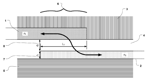
As illustrated in Figure 1, a first waveguide 1 is placed nearby (adjacent)
and parallel to
a second waveguide 2. The first waveguide is made of a low refractive index
material
having a refractive index n1. The second waveguide is made of a high
refractive index
material having a bulk refractive index n2. The first waveguide is surrounded
by
cladding materials, or material combinations 3, and 4 (and 5), propagates a
light signal
of a given wavelength with a given polarization, and has an effective index
neff1 of its
fundamental mode. The second waveguide 2 is surrounded by cladding materials,
or
material combinations 4 and 5 (and 3), propagates a light signal of the same
wavelength and same polarization, and has an effective index neff2 of its
fundamental
mode equal or close in value to neff1. The effective refractive indexes
mentioned
herein are always with respect to the fundamental modes. It is understood that
the
above layers and waveguides are wafer-level fabricated on a substrate (10).
In accordance with the proposed solution, the high refractive index material
thickness 7
(t1) of the second waveguide 2 can be optimized to allow the effective index
neff2 to be
equal to or close to neff1. As illustrated on Figure 2b, the physical
properties of the
materials employed in fabricating the silicon second waveguide 2 are such that
the
effective refractive index of the silicon waveguide changes abruptly with
silicon
waveguide thickness 7. A similar abrupt change is experienced by waveguides
16
CA 02822685 2013-06-21
WO 2012/088610 PCT/CA2011/050814
including germanium and to some extent in materials characterized as III-V
semiconductors which can be useful for optoelectronics.
The overlapping region 6 (L1) between the two waveguides 1 and 2 can be
optimized to
provide the best optical power transfer possible from one waveguide to the
other. The
extent of the overlap along the waveguides is known as coupling length
(distance) Lc.
A waveguide separation distance 8 (illustrated dl in Figure 1), for example
implemented
via a waveguide separation layer of cladding material 4, is small enough to
allow
directional optical coupling phenomena such as tunneling to take place.
Directional
coupling occurs via an extension of the evanescent field from the propagating
mode of
an input waveguide propagating light which enters the core of a neighboring
output
waveguide.
Figure 2a illustrates a plot of the effective refractive index neff2 as a
function of the high
refractive index material thickness 7 (t1) for a given waveguide width, a
given
wavelength and a given polarization. The variation illustrates a high
tuneability of the
effective index neff2 by controlling the high refractive index material
thickness 7 (t1).
Figure 2b illustrates a plot of the effective refractive index neff2 in the
case where silicon
is the high refractive index material. Both polarization states TE and TM are
illustrated
on the plot. It has been discovered that this coupling arrangement
exhibits a
polarization dependence as the high refractive index waveguide thickness 7
(t1) cannot
be optimized for both polarization states at the same time. Several
applications benefit
from this effect.
Figure 2c illustrates a variation of coupling efficiency as a function of the
effective
refractive index detuning between the intermediary 1 and the high refractive
index 2
waveguides. Directional coupling is most efficient when the effective
refractive indices
of the two waveguides are very close in value.
Figure 2d illustrates an example plot of the effective refractive index as a
function of
waveguide width for an optimized high refractive index thickness. It has been
discovered that the effective index has much less sensitivity with respect to
the width
17
CA 02822685 2013-06-21
WO 2012/088610 PCT/CA2011/050814
parameter. Therefore, fabrication constraints with respect to the lateral
dimension of
the waveguide can be relaxed.
Figure 2e illustrates an example plot of the coupling efficiency as a function
of the
waveguide misalignment illustrating that in the proposed configuration(s),
this parameter
is not highly critical.
Figures 3a, 3b and 3c illustrate another embodiment of the proposed solution
in
accordance with which the first waveguide 1 includes an optical fiber 9 having
an at
least partially exposed core 12. The optical fiber has some of its cladding 10
removed
in a way that allows its core 12 to be placed close enough to the high
refractive index
waveguide 2, for example by removing a portion of the cladding to provide a
facet. The
invention is not limited to the circular cross-section cladding and core fiber
illustrated in
Figure 3c. Figures 3a and 3b equally illustrate optical fibers with
rectangular cores, and
optionally with rectangular cladding. It has been found that a mismatch
between a
circular geometry of an optical fiber core 1, 12 compared to the rectangular
geometry of
the first waveguide 1 of Figure 1 does not have a significant impact on the
coupling
efficiency and comparable waveguide separations can be employed when the
geometries are dissimilar. With reference to figures 3a and 3c, the fiber core
12 comes
near or in contact with the waveguide separation layer 4 and is the first
waveguide 1.
Figure 3b illustrates that a mechanical positioning structure could be
fabricated at the
same time as the chip to allow easy positioning of the optical fiber. A
polymer 11 can
be used for fixing the optical fiber in place. (Further packaging and
alignment structure
details are presented herein below with reference to Figures 4a, 4b, 4c, 5a,
5b, 5c, 14a,
14b, 16a, 16b and 16c)
Figures 4a, 4b and 4c illustrate another embodiment including an optical fiber
9 butt-
coupled to an intermediary waveguide 1. For certainty, Figures 4a and 4b are
not
limited to circular optical fibers with circular cores and apply equally well
to optical fibers
having rectangular cross-section cores, and optionally rectangular cross-
section
cladding. Figure 4c illustrates a V-groove approach for the positioning of an
optical fiber
having a circular cross-section cladding with respect to the intermediary
waveguide.
The circular cross-section optical fiber geometry is illustrated in dashed
line for clarity,
18
CA 02822685 2013-06-21
WO 2012/088610 PCT/CA2011/050814
however the invention is not limited circular cross-section optical fibers.
For a
rectangular cross-section core and circular cross-section optical fiber, the
core would be
illustrated by a dashed rectangle 12 (not shown). The intermediary low
refractive index
waveguide 1 is built on top of the high (intrinsic/material) refractive index
waveguide 2.
The invention is not limited to the V-groove alignment structure 14, other
alignment
structures fabricated for example by lithography, etching and/or deposition
can be used.
The shape of the optical fiber can be employed for proper alignment. Figure 4d
illustrates the use of a polymer 11 ensuring a tight and refractive index
matched
interface between the fiber and the chip. (Further packaging and alignment
structure
details are presented herein below with reference to Figures 3a, 3b, 3c, 5a,
5b, 5c, 14a,
14b, 16a, 16b and 16c)
In accordance with another implementation illustrated in Figures 5a, 5b and
5c, a bus of
optical fibers dock on the chip, each optical fiber in the bus coupling to a
corresponding
semiconductor waveguide structure. Each fiber directs its carried optical
signal to
where on the integrated circuit the optoelectronic component is located. For
example
the optical fiber bus can form an array. The fiber bus and I/O waveguides can
be
provided in a package that connects on top of the integrated circuit package
as a
standard module. The integrated circuit can be fabricated with its tunneling
coupling
waveguides flush with the surface of the integrated circuit package and
hermetically
sealed. For example multiple tunneling coupling waveguides can be wafer level
fabricated in an array corresponding to an arrayed optical fiber bus on a
socket.
(Further packaging and alignment structure details are presented herein below
with
reference to Figures 3a, 3b, 3c, 4a, 4b, 4c, 14a, 14b, 16a, 16b and 16c)
For certainty, while in the above presented embodiments the high refractive
index
waveguide 2 is disposed under the first intermediary waveguide 1, the
invention is not
limited to such orientation. Figures 6a, 6b and 6c respectively illustrate
side, top and
cross-sectional views of an embodiment where the high refractive index
waveguide 2 is
built on top of the intermediary low refractive index waveguide 1.
Figure 7a illustrates an embodiment in which the coupling length 6 is
controlled by a
lateral deviation of the intermediary waveguide 1 while Figure 7b illustrates
another
19
CA 02822685 2013-06-21
WO 2012/088610 PCT/CA2011/050814
embodiment in which the coupling length 6 is controlled by deviating the high
refractive
index waveguide 2. It is also to be noted that the coupling length 6 can be
controlled by
deviating both coupling waveguides. Controlling the coupling length 6 controls
the
length of a standing wave pattern within the corresponding wave guide, the
length of the
sanding wave pattern determining the degree of light (optical signal)
coupling. The
angle of lateral deviation can vary within a range being only limited by
bending losses of
the waveguide(s).
Figures 8a to 8c illustrate implementations of an embodiment providing optical
signal
distribution from an input waveguide to a waveguide bundle having multiple on-
chip
waveguides. The coupling lengths 6, 6' and 6" are controlled individually to
transfer the
desired amount (fraction) of the input optical power to each semiconductor
waveguide 2
in the bundle. For example, if the input power of a single wavelength optical
signal has
to be split between two output waveguides 2, the first coupling would be
limited to a
50% of the input power and the second subsequent coupling would couple 100% of
the
remaining power (which is 50% of the input power). If the input optical signal
is a multi-
wavelength optical signal, it is envisioned that each coupling length 6 can be
separately
configured to couple 100% of the signal power of a corresponding wavelength
into a
corresponding semiconductor waveguide 2 of the bundle. Figure 8c illustrates
100%
coupling of an input optical signal into a semiconductor waveguide 2, and a
signal or
power dispatching structure 25, for example an MMI coupler, apportions the
power to a
number of semiconductor waveguides 26 in a bundle.
Figures 9a to 9c illustrate implementations of an embodiment providing
combination of
multiple optical signals from a bundle having many input waveguides to one on-
chip
waveguide. As above, coupling lengths 6, 6' and 6" can be employed to couple
particular fractions of input optical power signals, as well to couple
different wavelengths
in to a semiconductor waveguide 2. Figure 9c illustrates power or signal
dispatching
structure 27, for example an MMI coupler, which combines a bundle of multiple
inputs
12, 28 into a single output coupled to an intermediary (first) waveguide 1.
The very high efficiency dependency on the polarization can be used as an
advantage
in the case where one aims at separating the two polarizations. While
polarization
CA 02822685 2013-06-21
WO 2012/088610 PCT/CA2011/050814
dependency of the proposed solution is advantageous in such applications, such
polarization dependency is not necessarily a drawback. The following
embodiments
describe polarization mode recombination after coupling:
Figures 10a, 10b and 10c illustrate an embodiment providing simultaneous
(double)
coupling of both polarizations of an optical signal. Double coupling into a
bundle of
waveguides can be realized by placing the second waveguide 2 and a third
waveguide
2' in proximity to the first waveguide 1. Also, since the optimal high
refractive index
material thickness has to be tuned differently for each polarization, the
second
waveguide 2 and said third waveguide 2' are of different thicknesses, as well
the
coupling lengths 6, 6' are optimized separately for the high refractive index
material
waveguides 2, 2'.
With the second waveguide 2 and the third waveguide 2' placed side to side in
the
bundle, recombination can be achieved by merging the second waveguide 2 and
the
third waveguide 2' at some (downstream) point, for example through a Y
junction, to
add the two polarizations together into a single waveguide. Difference in
thicknesses
(7) t1, t1' between the second 2 and the third 2' waveguides are illustrated
in Figure
10b.
Figures 11a and 11b illustrate another embodiment providing simultaneous
(double)
coupling of both polarizations of an optical signal. The second 2 and third 2'
waveguides in the bundle are placed under and above the first waveguide 1.
Again, the
thickness (7) and the coupling lengths 6, 6' of the second waveguide 2 are
optimized
differently than those of the third waveguide 2'.
Figure 12 illustrates an embodiment providing simultaneous (double) coupling
of both
polarizations of an optical signal and recombination into the same waveguide
2. The
second waveguide 2 has two different sections defined by at least two
different
thicknesses t1, t1'. The first section has a thickness t1 and coupling length
6 optimized
for the coupling of a first polarization state and the second section has a
thickness t1'
and coupling length 6' optimized for the coupling of the second polarization
state.
21
CA 02822685 2013-06-21
WO 2012/088610 PCT/CA2011/050814
While not shown, different materials can be employed for the fabrication of
the second 2
and the third 2' waveguides in order to provide simultaneous coupling both
polarization
into respective semiconductor waveguides 2, 2'.
The invention is not limited to one layer SOI-CMOS chips, and applies equally
to chips
having multiple layer waveguide structures, for example biochips and
telecommunications chips.
Figure 13a is a schematic diagram illustrating, in
accordance with a further embodiment of the proposed solution, a side view of
a coupler
structure having at least four waveguide layers. Also, the invention is not
limited to
coupling optical signals traveling from outside of the chip to inside the chip
and vice-
versa, the signal coupling techniques described herein can be adapted to
transfer an
optical signal from layer to layer of a multilayer waveguide chip as
illustrated in Figure
13a. Intermediary waveguides transferring optical signal between layers are
referred to
as transfer waveguides.
Figure 13b is a schematic diagram illustrating a top view of the same coupler
structure
illustrating that only some of the waveguides (1) need to be compatible in
terms of butt-
coupling with optical fibers.
While the above description has made reference to butt-coupling on chip die
side
facets, the invention is not limited thereto:
Figure 14a illustrates an upturned
intermediary waveguide 1 enabling a butt-coupling with an optical fiber 12 on
a top chip
die surface. Alternatively, (not shown) the optical fiber 12 could itself be
bent instead of
the intermediate waveguide 1.
Similarly Figure 14b illustrates the use of an input waveguide block structure
18
configured to provide butt-coupling between the optical fiber 12 and the
intermediary
waveguide 1 enabling a butt-coupling of the optical fiber 12 on a top chip die
surface.
The input structure 18 redirects the optical signal into the waveguide 1
plane.
For packaging and socket type optical signal coupling purposes, curved
waveguides
and/or input/output waveguide block structures (18) can be employed for
ensuring
correct alignment. In some implementations a microscope can be employed to
ensure
correct alignment, with reference to Figures 2d, 2e, 10a and 10b some degree
of
22
CA 02822685 2013-06-21
WO 2012/088610 PCT/CA2011/050814
misalignment can be tolerated. (Further packaging details are presented herein
below
with reference to Figures 3a, 3b, 3c, 4a, 4b, 4c, 5a, 5b, 5c, 16a, 16b and
16c)
The invention is not limited to external generation of the optical signal.
Figures 15a and
15b are schematic diagrams illustrating, in accordance with a further
embodiment of the
proposed solution, an optical signal transport structure between light sources
31 and/or
photodetectors 31' mounted on the same chip.
Figures 16a, 16b and 16c are schematic diagrams illustrating, in accordance
with a
further embodiment of the proposed solution, side, top and cross-sectional
views of a
flip-chip packaged device. The first (effective low refractive index)
waveguide 1 is built
into the package and the high refractive index waveguide 2 is built on top of
the chip in
a flipped wafer structure. A filling polymer 34 is chosen to have good optical
properties
and a refractive index lower than that of the effective low refractive index
of waveguide
1. For example filling polymer 34 can be applied in fluid form and cured. The
routing of
the optical waveguides takes into account positions of flip-chip bonding
contact beads
35. For certainty in Figures 16a to 16c top and bottom relationships are
interchangeable, the layered structure would operate identically if all layers
were
illustrated in reverse vertical order as illustrated with reference to Figures
5a to 5c. The
only reason Figures 16a to 16c have the illustrated orientation is to simplify
understanding of the application of the filing polymer 34 in a single step.
When
waveguide(s) 1 are provided in a socket providing attachment to a chip
including
waveguide 2, filling polymer 34 can be omitted assuming that refractive index
requirements are present or replaced by another structure not requiring fluid
form
application having the requisite refractive index. Curing of a fluid filling
polymer 34 may
or may not be required. Filling polymer 34 can also include a gelatinous
material having
high viscosity (and/or variable viscosity).
While packaging details presented herein above with reference to Figures 3a,
3b, 3c,
4a, 4b, 4c, 5a, 5b, 5c, 14a, 14b, 16a, 16b and 16c have concentrated on
vertical
alignment, xy-alignment mentioned herein above with reference to Figure 5 can
be
provided for implementing packaging aspects and features for example to
implement a
socket for optical signal coupling to and from an integrated chip. With
reference to an
23
CA 02822685 2013-06-21
WO 2012/088610 PCT/CA2011/050814
inverted Figures 16a and 16c, the flip-chip layered structure including layers
5' and 1
separately fabricate for example as a socket, can be positioned with respect
to the
layered structure including layers 10, 5, 4 and 2 on a mounted chip by
employing at
least one alignment structures. In some implementations a microscope can be
employed to ensure correct alignment, with reference to Figures 2d, 2e, 10a
and 10b
some degree of misalignment can be tolerated.
For vertical alignment, beads 35 and/or V-groves as illustrated in Figures 3b,
3c, 4b and
4c can be employed. Sockets having an array of optical fiber waveguides 1
corresponding to an array of on-chip waveguides 2, need not necessarily have
circular
cross-section cores and/or circular cross-section claddings. Furthermore, when
V-
groves are employed for vertical alignment of a waveguide 1 array, V-groves
are not
required for each optical fiber. A combination of V-groves and beads 35 can
also be
employed.
Alignment structures, for example employing beads 35 and/or V-groves (Figures
3b, 3c,
4b and 4c) can also be employed for xy-alignment or at least one waveguide 1.
When
an array of waveguides 1 of a socket are to be coupled to an array of
waveguides 2 on
a chip, the invention is not limited to a one-to-one correspondence between xy-
alignment structures and waveguides in corresponding arrays. Properties of
polymer 34
alluded to above can for example be provided by a gelatinous material of high
viscosity
(and/or variable viscosity) which may or may not require curing.
With optical signal coupled into the thinned (second) semiconductor high
refractive
index waveguide 2, the optical signal continues propagation along
semiconductor
waveguide 2 to interface with the rest of the chip. In
accordance with one
implementation, optical circuitry of the chip could consist only of
semiconductor
waveguides having a thickness substantially equal to the optimal thickness
high
refractive index waveguide 2 at the coupling device. In accordance with
another
implementation, a transition between thinned semiconductor waveguides 2
configured
for coupling optical signals and regular thickness semiconductor waveguides is
provided. The transition is configured to minimize optical signal losses, for
example by
24
CA 02822685 2013-06-21
WO 2012/088610 PCT/CA2011/050814
gradually (smoothly) varying the thickness. In certain applications abrupt
transitions can
also be employed (to generate desired effects).
Figure 17a is a schematic diagram illustrating a first step of a LOCal
Oxidation of Silicon
(LOCOS) process for wafer level fabrication of semiconductor waveguides 2 of
controlled thickness. A cover material layer 39 deposited on top of a silicon
layer 38,
acts as an oxidation mask (barrier) to silicon layer 37 to be oxidized.
Without limiting
the invention, layer 39 includes silicon nitride however other oxidation mask
materials
can be employed. The thickness of the barrier layer 39 has to be large enough
to block
oxygen diffusion therethrough. Layer 38 for example consists of silicon
dioxide and can
be used to prevent delamination of the oxidation mask layer 39. The thickness
of the
oxide layer 38 can be a few tenths of a nanometer.
Figure 17b is a schematic diagram illustrating a second step of the LOCOS
process.
Layer 38 is known as a silicon dioxide growth layer when exposed to high
temperature
oxidation. The oxide growth from the silicon layer 37' is limited by oxygen
diffusion and
has a tendency to produce a smooth transition between masked and unmasked
regions. Oxidation control in this step provides thickness selection (control)
in the high
refractive index waveguide. For example, the silicon high refractive index
waveguide
layer is thinned down to a thickness between 20nm and 200nm by use of a
standard
oxidation process or an etching process.
Figure 17c is a schematic diagram illustrating a third step of the LOCOS
process, where
the masking layer and the deposited silicon dioxide growth layer have been
removed.
The removal procedure, for example includes a selective hydrofluoric acid
based etch.
The resulting silicon layer thickness is optimized for optical coupling with
the low
refractive dielectric transient waveguide (intermediary waveguide) 1 in the
unmasked
regions.
For certainty, the invention is not limited to the silicon layer 37, for
example germanium,
III-V materials, etc. useful for optoelectronics can also be employed.
Figure 18a is a schematic diagram illustrating a first step of a shadow
masking process.
Support blocks 41 are built from a photoresist pattern or another suitable
material. A
CA 02822685 2013-06-21
WO 2012/088610 PCT/CA2011/050814
shadow mask 42 is also built from a photoresist or another suitable material,
for
example a bonded silicon wafer or deposited metal layers.
Figure 18b is a schematic diagram illustrating a second step of the shadow
mask
process. Either, the high refractive index waveguide material 37 or a suitable
masking
material 44, 44' could be deposited employing a chemical or physical
deposition
procedure (CVD, Sputtering, etc.). It is noted that the shadow mask could also
be used
to directly etch the high refractive index waveguide layer 37 to thin it down
to an optimal
thickness. Shadow masking has proven to be efficient in both deposition and
etching.
The spacing 40 between the shadow mask 42 and the wafer surface affects the
transition profile leading to a tapered transition.
Figure 18c is a schematic diagram illustrating a third step of the shadow mask
process,
wherein the shadow mask is removed which leaves the deposited layer 44 having
a
smooth transition between the fully exposed region and the shadowed region. It
is
noted that a similar transition would have been left subsequent to etching in
the second
step.
Figure 18d is a schematic diagram illustrating a fourth step of the shadow
mask
process, where the tapered etch mask 44' profile is transferred to the high
refractive
index waveguide layer 37' removing both mask 44' and high refractive index
waveguide
material in substantially equal amounts, as the mask 44' retreats. Such
removal can be
provided via various means, including chemical (etching), physical (plasma
etching,
ablation), etc. The tapered region provided by the deposition in the presence
of a
separated shadow mask results in a high refractive index waveguide regions of
different
thickness, wherein the first region (2) is tuned for optimal optical power
transfer from or
to a (dielectric) waveguide 1. The remaining waveguide layer 37' has a smooth
transition between the masked and unmasked regions.
Figure 18e is a schematic diagram illustrating a fifth step of the shadow mask
process,
wherein any masking material 44' is selectively removed, only the high
refractive index
waveguide layer 37' remains forming the semiconductor waveguide 2.
26
CA 02822685 2013-06-21
WO 2012/088610 PCT/CA2011/050814
Figure 19a and 19b are schematic diagrams illustrating, in accordance with the
proposed solution, top and cross-sectional views of yet another embodiment
wherein
the low refractive index (transient) waveguide 1 and the high refractive index
waveguide
2 are built side by side on a wafer 10. A high performance etching process is
employed
to achieve the illustrated aspect ratios in the high refractive index
waveguides, for
example employing a shadowing mask during deposition.
Applications:
The proposed solution can be applied to the chip-to-chip optical interconnects
for
CMOS integrated circuits. With standard device layer thickness of about 220nm,
efficient directional coupling cannot take place between a standard optical
waveguide
having a standard effective index between 1.4 and 1.6. By thinning down some
regions
of the silicon device layer to an optimal coupling thickness, 501 CMOS chips
can be
manufactured to enable light coupling to and from an optical waveguide made of
a low
refractive index material which is used to link two or more CMOS chips.
(Figures 5a to
5c)
The proposed solution can be also applied to in / out coupling of an optical
signal for
high intensity evanescent field biosensors. Such sensors require a high
refractive
guiding index layer to produce a high intensity evanescent field right above
the
waveguide layer which the proposed solution provides.
Otherwise, in such
configurations, butt-coupling to an optical fiber is known to be inefficient.
With reference to Figures 13a and 13b, the proposed solution can be employed
to
implement an intra-chip inter-layer optical signal transfer between multiple
layers. Such
structures can be used in microelectronic chips and bioelectronic devices.
With reference to Figures 15a and 15b, the proposed solution can be employed
to
implement an optical coupling internal to a chip between optical sources and
detectors
are implemented directly on the chip.
27
CA 02822685 2013-06-21
WO 2012/088610 PCT/CA2011/050814
Simplicity of fabrication is one of the advantages of the proposed solution.
Very high
optical signal injection efficiency into a high refractive index material can
be obtained by
employing low resolution lithographic techniques. The proposed solution
essentially
provides a 2D solution to address the problem. Furthermore, this permits
employing a
large variety of materials, including germanium based semiconductor materials
and
materials characterized as III-V semiconductors which are useful for
optoelectronics.
Another advantage of the proposed solution is derived from a much reduced
sensitivity
to misalignment (Figure 2e), which is of a great benefit in chip packaging
(embedding
the chip die in resin).
Another advantage provided by the proposed solution is derived from facet
injection
(chip edge injection) which permits very easy alignment. This is important
because,
currently a large fraction of chip component packagers are reluctant to adopt
surface
injection.
The single inconvenience of the proposed solution stems from polarization
dependence.
A choice must be made between coupling the incident TM mode or the incident TE
mode. Little importance is ascribed to such inconvenience, because many
existing low
cost solutions can be employed to change the polarization outside of the chip
or on
chip. For example, in certain applications, this shortcoming can be
employed
strategically, purposefully, to produce an incident wave separation effect,
for example to
implement a beam splitter. The polarization dependence can be highly
diminished by
reducing the width of the high refractive index waveguide to a dimension of
the order of
that of the thickness thereof.
For certainty while extensive reference has been made to silicon semiconductor
waveguides, such reference has only been made for ease of understanding. The
invention is not limited to silicon based waveguides and the proposed solution
also
applies for example to waveguides containing germanium, III-V materials, and
others
which can be useful for optoelectronics applications.
28
CA 02822685 2013-06-21
WO 2012/088610 PCT/CA2011/050814
While the invention has been shown and described with reference to preferred
embodiments thereof, it will be recognized by those skilled in the art that
various
changes in form and detail may be made therein without departing from the
spirit and
scope of the invention as defined by the appended claims.
29