Note: Descriptions are shown in the official language in which they were submitted.
CA 02822811 2013-06-21
WO 2012/087901
PCT/US2011/065774
COMMUNICATIONS ARCHITECTURE FOR PROVIDING DATA
COMMUNICATION, SYNCHRONIZATION AND FAULT DETECTION
BETWEEN ISOLATED MODULES
CROSS-REFERENCE TO RELATED APPLICATIONS
[01] This application claims priority under 35 U.S.C. 119(e)
from provisional
U.S. patent application no. 61/426,081, entitled "Communication Architecture
for
Multilevel Power Converter" and filed on December 22, 2010, the contents of
which are
incorporated herein by reference.
BACKGROUND OF THE INVENTION
1. Field of the Invention
[02] The present invention pertains to an electronic system (such as,
without
limitation, a multilevel power inverter or an active front end) that employs
multiple
modules (wherein each module may include one or more printed circuit boards
(PCBs)
and/or other electronic components), and, in particular, to a communications
architecture
for providing data communication, synchronization and fault detection between
isolated
modules in such an electronic system.
2. Description of the Related Art
[03] A number of different power conversion modules/systems are well
known
for converting power from one form to another. For example, a multilevel power
inverter is a power electronic device that is structured to produce AC
waveforms from a
DC input voltage. As another example, an active front end (also called a
controllable
rectifier) is a power electronic device wherein AC waveforms are converted to
DC
voltages. Such power conversion modules/system are used in a wide variety of
applications, such as, without limitation, variable speed motor drives, and
frequently
require highly synchronized timing across communication links of the system
and/or fast
fault response between links in the system.
[04] Many current industrial electronic systems employ asynchronous
data
communications (wherein no serial clock (SCLK) is employed) and require
specialized
physical interfaces and topologies. These asynchronous topologies require one
of the
- 1 -
CA 02822811 2013-06-21
WO 2012/087901
PCT/US2011/065774
following solutions to provide synchronization: (i) timestamp messages, which
require
dedicated hardware and processing time, or (ii) a completely separate
communication line
used solely for synchronization (which adds additional connections such as
additional
optical fibers).
[05] Many current systems utilize the timestamp method to keep
synchronization.
A case example is the IEEE 1588 specification which allows synchronization
across
Ethernet networks. The standard requires that specialized timestamp hardware
be included
in each node's Ethernet system. Additionally, a central hub/switch must also
be added to
the system to meet the standard Ethernet star topology. While only two optical
fibers would
be needed for each module to implement such a system, the central hub/switch
would also
need two optical fibers. Unfortunately, fiber optic Ethernet hubs/switches are
not as
common or cost effective as their copper counterparts. Additional downsides
include
sacrificing some of the communication bandwidth to provide time for the
synchronization
messages to be broadcast.
[06] In addition, the well known EtherCATO system is a variant of the IEEE
1588 specification where the synchronization is done entirely in hardware, and
a ring
topology is used instead of a star. No switches are required, but each module
must have
two datapaths to provide round trip information, which is needed for the
synchronization.
These two data paths require four fiber transceivers per module (2 IbdTx
pairs). Also, the
required EtherCATO hardware interface integrated circuit (IC) adds additional
cost and
integration effort.
[07] None of the standard communication solutions appears to provide a
dedicated way to flag a fault quickly without sending a specific data message
(note that
sending a fault data message is not desirable as the message must be fully
received and
decoded before fault actions can occur, leading to relatively slow detection
performance).
The common way to provide a fast fault line has been to provide a dedicated
healthy line
that any node on the system can pull down when a problem is detected. The
problem with
such a system is that it requires an additional fiber interface that is not
part of the actual
communication scheme.
- 2 -
CA 02822811 2013-06-21
WO 2012/087901
PCT/US2011/065774
[08] Thus, there is a need for a communication architecture that provides
an
efficient way to communicate data and synchronization information that may be
employed
in an electronic system such as, without limitation, a power conversion
module/system
(e.g., a multilevel power inverter or an active front end).
SUMMARY OF THE INVENTION
[09] In one embodiment, an electronic system, such as, without limitation,
a
multilevel power inverter foiiiiing part of a motor drive, is provided. The
system
includes a master module having a first control unit, the first control unit
having one or
more first serial interfaces (e.g., SPI interfaces), the first control unit
being programmed
to output a first data signal and a first clock signal through the one or more
first serial
interfaces, and a slave module having a second control unit, the second
control unit
having a second serial interface (e.g., an SPI interface). The slave module
receives the
first clock signal through the second serial interface, and the second control
unit is
programmed to monitor the slave module for a fault condition and output a
second clock
signal through the second serial interface which is (i) the same as the first
clock signal if a
fault condition on the slave module is not detected, and (ii) a modified clock
signal
having a predetermined format if a fault condition on the slave module is
detected.
[10] In another embodiment, a method of providing synchronization
information and fault detection information in an electronic system is
provided. The
method includes generating a first data signal and a first clock signal in a
master module
of the electronic system, the master module having one or more first serial
interfaces, and
outputting the first data signal and the first clock signal from the master
module through
the one or more first serial interfaces. The method further includes receiving
the first
clock signal through a second serial interface of a slave module of the
electronic system,
and monitoring the slave module for a fault condition on the slave module.
Finally, the
method includes, responsive to receiving the clock signal in the slave module,
outputting
a second clock signal through the second serial interface to either the master
module or an
additional slave module of the electronic system which is (i) the same as the
first clock
- 3 -
CA 02822811 2013-06-21
WO 2012/087901
PCT/US2011/065774
signal if a fault condition on the slave module is not detected, and (ii) a
modified clock
signal having a predetermined format if a fault condition on the slave module
is detected.
11.1] These and other objects, features, and characteristics of
the present
invention, as well as the methods of operation and functions of the related
elements of
structure and the combination of parts and economies of manufacture, will
become more
apparent upon consideration of the following description and the appended
claims with
reference to the accompanying drawings, all of which form a part of this
specification,
wherein like reference numerals designate corresponding parts in the various
figures. It is
to be expressly understood, however, that the drawings are for the purpose of
illustration
and description only and are not intended as a definition of the limits of the
invention.
BRIEF DESCRIPTION OF THE DRAWINGS
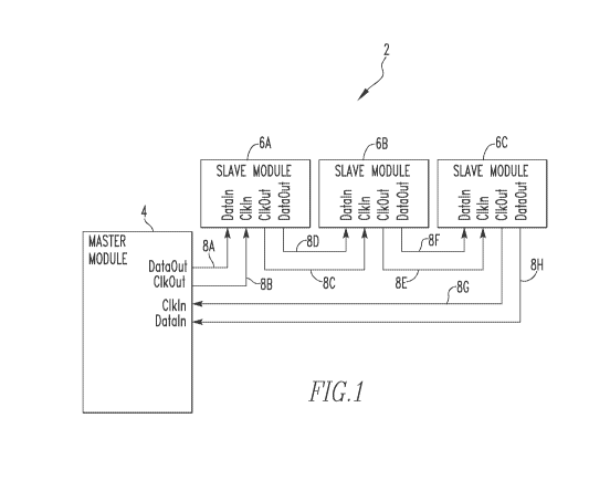
[12] FIG. 1 is a schematic diagram of an electronic system that implements
a
communications architecture of the present invention according to one
particular, non-
limiting exemplary embodiment;
[13] FIG. 2 is a schematic diagram of master module forming part of the
electronic system of FIG. 1 according to an exemplary embodiment;
[14] FIG. 3 is a schematic diagram of slave module forming part of the
electronic system of FIG. 1 according to an exemplary embodiment;
[15] FIG. 4 shows an oscillating clock signal employed in a discontinuous
SPI
scheme as may be used to implement the present invention;
[16] FIG. 5 shows a modified oscillating clock signal employed in the
present
invention to indicate faults;
[17] FIG. 6 is a schematic diagram of an electronic system that implements
a
communications architecture of the present invention according to an
alternative
particular, non-limiting exemplary embodiment;
[18] FIG. 7 is a schematic diagram of master module forming part of the
electronic system of FIG. 6 according to an exemplary embodiment;
- 4 -
CA 02822811 2013-06-21
WO 2012/087901
PCT/US2011/065774
[19] FIG. 8 is a schematic diagram of an electronic system that implements
a
communications architecture of the present invention according to another
alternative
particular, non-limiting exemplary embodiment;
[20] FIG. 9 is a schematic diagram of master module forming part of the
electronic system of FIG. 8 according to an exemplary embodiment; and
[21] FIG. 10 is a schematic diagram of an electronic system that implements
a
communications architecture of the present invention according to still
another alternative
particular, non-limiting exemplary embodiment.
DETAILED DESCRIPTION OF EXEMPLARY EMBODIMENTS
[22] As used herein, the singular form of "a", "an", and "the" include
plural
references unless the context clearly dictates otherwise. As used herein, the
statement
that two or more parts or components are "coupled" shall mean that the parts
are joined or
operate together either directly or indirectly, i.e., through one or more
intermediate parts
or components, so long as a link occurs. As used herein, "directly coupled"
means that
two elements are directly in contact with each other. As used herein, "fixedly
coupled" or
"fixed" means that two components are coupled so as to move as one while
maintaining a
constant orientation relative to each other.
[23] As used herein, the word "unitary" means a component is created as a
single piece or unit. That is, a component that includes pieces that are
created separately
and then coupled together as a unit is not a "unitary" component or body. As
employed
herein, the statement that two or more parts or components "engage" one
another shall
mean that the parts exert a force against one another either directly or
through one or
more intermediate parts or components. As employed herein, the term "number"
shall
mean one or an integer greater than one (i.e., a plurality).
[24] Directional phrases used herein, such as, for example and without
limitation, top, bottom, left, right, upper, lower, front, back, and
derivatives thereof, relate
to the orientation of the elements shown in the drawings and are not limiting
upon the
claims unless expressly recited therein.
- 5 -
CA 02822811 2013-06-21
WO 2012/087901
PCT/US2011/065774
[25] The present invention, in the exemplary embodiment, provides a
communications architecture that may be used for module to module
communications in
an electronic system (wherein each module may include, for example and without
limitation, one or more printed circuit boards (PCBs) and/or other electronic
components). In one particular, non-limiting embodiment, the architecture is
employed
in a multilevel power inverter implemented using multiple modules. For
example, and
without limitation, United States Provisional Application No. 61/426,051,
filed on
December 22, 2010, and United States Provisional Application No. 61/501,876,
filed on
June 28, 2011, each owned by the assignee of the present invention and
entitled
"Mechanical Arrangement of a Multilevel Power Converter Circuit," describe
particular
alternative mechanical arrangements for a multilevel power inverter, and it
will be
understood that the communications architecture described herein may be
employed with
such multilevel power inverter arrangements. The disclosures of United States
Provisional Application Nos. 61/426,051 and 61/501,876, and United Patent
Application
Serial No. _______ , filed on the same date herewith and claiming priority
under 35 U.S.C.
119(e) to the provisional applications just identified, are incorporated
herein by reference
in their entirety. A number of other topologies for implementing a multilevel
power
inverter are also well known, including the neutral point clamped (NPC)
topology, the
flying capacitor (FC) topology and the H-bridge topology, and it will be
understood that
the communications architecture described herein may be employed with any of
such
topologies, or any other known or hereafter developed topology that may be
used to
implement a multilevel power inverter. In another particular, non-limiting
embodiment,
the architecture is employed in an active front end implemented using multiple
modules
that each may include, for example and without limitation, one or more PCBs
and/or
other electronic components.
[26] The communications architecture described herein is, in the exemplary
embodiment, an enhancement of the widely known standard serial peripheral
interface
(SPI) synchronous protocol, which requires both a system clock signal (SCLK)
and a data
signal to be transmitted together. In the exemplary embodiment, and as
described in
- 6 -
CA 02822811 2013-06-21
WO 2012/087901
PCT/US2011/065774
greater detail herein, the communications links are formed using fiber optic
media and the
clock signal is used for multiple purposes, namely for both system
synchronization and
fast fault detection.
[27] Furthermore, in the communications architecture described herein, the
modules are set up in a single master, multiple slave arrangement as a
broadcast domain.
This allows the SPI to eliminate the NSS (slave select) signal, thereby saving
a fiber and
reducing complexity (NSS can be pulled up with hardware, or disabled within
the software).
In the exemplary embodiment, shown in FIG. 1 and described in detail herein,
the
modules are arranged in a daisy chain topology (although other topologies,
such as a star
or star and daisy chain topology, are also possible and are described
elsewhere herein as
alternatives) wherein each module acts as a fiber repeater, and wherein the
received
optical signals are converted to electrical signals. The electrical signals
are monitored by
a microcontroller and retransmitted to the next module in the chain as optical
signals.
This creates a simple broadcast domain, but at the cost of propagation delay
from the
optical to electrical conversions. As described in greater detail herein, each
slave module
will have a microcontroller and an SPI with supporting circuitry for receiving
the SCLK
and data signals (ClkIn and DataIn) and for transmitting the SCLK and data
signals
(ClkOut and DataOut). Also, the SPI will have associated with it two RX
optical to
electrical converters for converting the received optical ClkIn and DataIn
signals to
electrical signals and two TX electrical to optical converters for converting
electrical
ClkOut and DataOut signals on the module to optical signals that may be
transmitted to
the next module over the fiber link. The microcontroller on each module has
the ability
to add feedback data to the DataOut signal.
[28] In addition, by using a discontinuous SPI communication scheme in the
communications architecture, the SCLK signal is used for both synchronization
and fault
detection communication. In particular, in one exemplary implementation,
discontinuous
SPI stops transmitting the SCLK oscillating signal for short amounts of time
between
messages. This will appear as a logic low gap in the SCLK signal which can be
detected
by the modules. Furthermore, the microcontroller is programmed to, in the
event that a
- 7 -
CA 02822811 2013-06-21
WO 2012/087901
PCT/US2011/065774
fault condition is detected on the module, pull the SCLK signal high and
transmit that
logic high signal rather than the SCLK signal it received to indicate a fault
to the other
modules. Each module will continuously monitor the SCLK signal and look for
gaps in
the oscillating signal. If a gap is detected, the logic level is measured to
determine
whether the gap is a synch signal or a fault signal. It will be understood
that the logic
high vs. logic low gap assignments (sync vs. fault) in a discontinuous SPI
communication
scheme can be arbitrary as long as the entire system is consistent in their
use. In other
words, in an alternative implementation of a discontinuous SPI communication
scheme,
logic high may be used for synch and logic low may be used for fault. For
illustrative
purposes, in the exemplary embodiments described herein, the former
implementation
(logic low for synch and logic high for fault) is used, but this is not mean
to be limiting.
[29] FIG. 1 is a schematic diagram of an electronic system 2 that
implements
the communications architecture of the present invention according to one
particular,
non-limiting exemplary embodiment. As seen in FIG. 1, electronic system 2
includes a
master module 4 and a number of slave modules 6 arranged in a daisy chain
configuration. Master module 4 and slave modules 6 are each described in
detail below.
In the illustrated, exemplary embodiment, electronic system 2 includes three
slave
modules 6, labeled 6A, 6B, and 6C. It will be understood, however, that this
is meant to
be exemplary only, and that electronic system 2 may include one, two or four
or more
slave modules 6 within the scope of the present invention.
[30] Master module 4 and slave modules 6A, 6B, and 6C are configured to
communicate with one another optically, and thus are coupled to one another in
the daisy
chain configuration of FIG. 1 by a plurality of fiber optic cables 8. In
particular, as seen
in FIG. 1, master module 4 has two optical data outputs, DataOut and ClkOut,
and two
optical data inputs, DataIn and ClkIn. Similarly, each slave module 6 has two
optical data
outputs, DataOut and ClkOut, and two optical data inputs, DataIn and ClkIn. As
seen in
FIG. 1, the DataOut and ClkOut of master module 4 are coupled to the DataIn
and ClkIn,
respectively, of slave module 6A by fiber optic cables 8A and 8B, the DataOut
and
ClkOut of slave module 6A are coupled to the Data,In and ClkIn, respectively,
of slave
- 8 -
CA 02822811 2013-06-21
WO 2012/087901
PCT/US2011/065774
module 6B by fiber optic cables 8D and 8C, the DataOut and ClkOut of slave
module 6B
are coupled to the Dataln and ClkIn, respectively, of slave module 6C by fiber
optic
cables 8F and 8E, and the DataOut and ClkOut of slave module 6C are coupled to
the
Dataln and ClkIn, respectively, of master module 4 by fiber optic cables 8H
and 8G.
[31] Referring now to FIG. 2, the structure of master module 4 according to
the
exemplary embodiment will be described. Master module 4 comprises one or more
printed circuit board having a number of components provided thereon. More
specifically, master module 4 includes a control unit 10, such as, without
limitation, a
microprocessor, a microcontroller, a field programmable gate array (FPGA), or
some
other suitable processing device. Control unit 10 includes two SPI interfaces,
SPI1 and
SPI2. SPI1 is configured to operate in master mode and includes an SPI1
DataOut output
(e.g., a pin/line) 12 and an SPI1 ClkOut output (e.g., a pin/line) 14. As
described in detail
elsewhere herein, control unit 10 is structured to generate a master data
signal and a
master clock signal and output those signals on SPI1 DataOut output 12 and
SPI1 ClkOut
output 14, respectively. SPI2 is configured to operate in slave mode and
includes an
SPI2 Dataln input (e.g., a pin/line) 16 and an SPI2 ClkIn input (e.g., a
pin/line) 18. As
also described in detail elsewhere herein, control unit 10 is structured to
receive a data
signal and a clock signal from slave module 6C on SPI2 Dataln input 16 and
SPI2 ClkIn
input 18, respectively.
[32] Master module 4 further includes two electrical to optical (E/O)
converters
20A, 20B. As seen in FIG. 2, E/O converter 20A receives the master data signal
in
electrical form ("Electrical DataOut") and converts it to optical forin
("Optical
DataOut"). That optical signal is transmitted on fiber optic cable 8A (FIG.
1). Similarly,
E/O converter 20B receives the master clock signal in electrical form
("Electrical
ClkOut") and converts it to optical form ("Optical ClkOut"). That optical
signal is
transmitted on fiber optic cable 8B (FIG. 1).
[33] Master module 4 also includes two optical to electrical (0/E)
converters
22A, 22B. As seen in FIG. 2, 0/E converter 22A receives the data signal from
slave
module 6C in optical fonn ("Optical Dataln") through fiber optic cable 811,
converts it to
- 9 -
CA 02822811 2013-06-21
WO 2012/087901
PCT/US2011/065774
electrical faun ("Electrical DataIn") and provides it to SPI2 Dataln input 16.
Similarly,
0/E converter 22B receives the clock signal from slave module 6C in optical
form
("Optical Clkln") through fiber optic cable 8G, converts it to electrical form
("Electrical
ClkIn") and provides it to SPI2 Clkln input 18.
[34] Referring now to FIG. 3, the structure of slave module 6 (e.g., 6A, 6B
and
6C) according to the exemplary embodiment will be described. Slave module 6,
like
master module 4, in the exemplary, non-limiting embodiment comprises one or
more
printed circuit boards having a number of components provided thereon. More
specifically, slave module 6 includes a control unit 24, such as, without
limitation, a
microprocessor, a microcontroller, an FPGA, or some other suitable processing
device.
Control unit 24 includes an SPI interface that is configured to operate in
slave mode.
That SPI interface includes an SPI Dataln input (e.g., a pin/line) 26, an SPI
DataOut
output (e.g., a pin/line) 28, and an SPI Clkln input (e.g., a pin/line) 30.
Control unit 24
further includes a timer input 32 to an internal timer, a multiplexer select
output 34, and a
buffer output enable output 40, the purposes of which are each described
below.
[35] Slave module 6 also includes an 0/E converter 42A that receives an
optical data signal ("Optical Dataln") that is received on the optical data
input ("Dataln")
of the slave module 6 and converts that optical signal into an electrical
signal ("Electrical
Dataln"). Slave module 6 further includes a second 0/E converter 42B that
receives an
optical clock signal ("Optical Clkln") that is received on the optical clock
input ("ClIdn")
of the slave module 6 and converts that optical signal into an electrical
signal ("Electrical
Clkln").
[36] In addition, as seen in FIG. 6, slave module 6 includes a 2-to-1
multiplexer
(MUX) 46 and an enabled buffer 48. The function of each of these components is
described in detail below.
[37] As seen in FIG. 3, the Electrical Dataln signal is provided to both
SPI
Dataln input 26 of control unit 24 and to the first input of MUX 46. The
second input of
MUX 46 is coupled to SPI DataOut output 28 of control unit 24. Further,
multiplexer
select output 34 of control unit 24 is provided to the select input of MUX 46
so that
-10-
CA 02822811 2013-06-21
WO 2012/087901
PCT/US2011/065774
control unit 24 can determine/select which of the two MUX inputs (Electrical
DataIn or
SPI DataOut) is output by MUX 46 as the "Electrical DataOut" signal.
[38] As also seen in FIG. 3, the Electrical ClkIn signal is provided to
three
places, namely SPI ClkIn input 30 of control unit 24, timer input 32 of
control unit 24,
and to the first input of buffer 48. If buffer output enable output 40 of
control unit 24 is
made active, the Electrical ClkIn signal will be output by buffer 48. If
multiplexer output
enable output 40 of control unit 24 is made inactive, buffer 48 will be caused
to output a
predetermined logic state, which is a logic high in the exemplary embodiment.
The
purpose of this is described elsewhere herein.
[39] Finally, slave module 6 further includes two electrical to optical
(E/O)
converters 50A, 50B. As seen in FIG. 3, E/O converter 50A receives the
Electrical
DataOut signal and converts it to optical form ("Optical DataOut"). That
optical signal is
transmitted on the associated fiber optic cable 8D, 8F, or 8Hshown in FIG. 1.
Similarly,
E/O converter 50B receives the Electrical ClkOut signal and converts it to
optical form
("Optical ClkOut"). That optical signal is transmitted on the associated fiber
optic cable
8C, 8E, or 8Gshown in FIG. 1.
[40] As noted elsewhere herein, master module 4 generates both command data
signals/messages and a system clock signal. In the exemplary embodiment, two
different
data frames are sent by master module 4: one for master commands from master
module 4,
and one for slave feedback from a selected slave module 6. The master commands
are
information from master module 4 to provide the slave modules 6 with the
needed
information to continue operating (example would be modulation depths for a
multilevel
drive system). The slave section is where a selected slave module 6 will
transmit feedback
data back to master module 4 (example would be current and voltage
measurements). The
particular selected slave module 6 is selected by master module 4 in the
previous command
data message as a transmitted ID number. This ID system prevents multiple
slave modules
6 from attempting to access the broadcast domain of electronic system 2 at the
same time.
[41] In addition, as also noted elsewhere herein, in the exemplary
embodiment,
electronic system 2 employs a discontinuous SPI scheme. As is known in the
art, in a
- 11 -
CA 02822811 2013-06-21
WO 2012/087901
PCT/US2011/065774
discontinuous SPI scheme, master module 4 is programmed to stop transmitting
the
system clock oscillating signal for short amounts of time between messages.
This will
appear as a logic low gap in the system clock signal as shown in FIG. 4.
Furthermore, in
this scheme, control unit 24 of each slave module 6 is programmed to, in the
event that a
fault condition is detected on slave module 6, pull the system clock signal
high and
transmit that logic high signal rather than the system signal it received to
indicate a fault
to the other slave modules 6. This is done by making the buffer output enable
output 40
of the control unit 24 inactive. The control unit 24 of that slave module 6
will also then
enter a predeteimined safe operating mode. Each other slave module 6 will
continuously
monitor the system clock signal it receives on its optical Clkin input and
look for gaps in
the oscillating signal using the timer input 32. If a gap is detected, the
logic level is
measured to determine whether the gap is a synch signal or a fault signal. If
a fault
signal, the control unit 24 of that slave module 6 will enter a safe operating
mode. In
addition, control unit 10 of master module 4 is programmed to, in the event
that a fault
condition is detected on master module 4, pull the system clock signal high
and transmit
that logic high signal rather than the nonnal system clock signal to indicate
a fault to the
slave modules 6. Master module 4 and the slave modules 6 will then enter a
safe
operating mode (the slave modules 6 will do so upon receipt of the logic high
signal as
described elsewhere herein).
[42] Operation of electronic system 2 will now be described in detail in
connection with the particular exemplary embodiments of FIGS. 2 and 3. First,
operation
of electronic system 2 will be described assuming that no faults in electronic
system 2
have occurred. This will enable normal operation of electronic system 2 to be
understood, including the flow of data and clock signals within electronic
system 2.
Thereafter, operation of electronic system 2 in the event of a fault condition
in one of the
modules will be described.
[43] When master module 4 needs to send a message to all slave modules 6A,
6B, 6C, it will generate a master command signal broadcast. None of the slave
modules
6A, 68, 6C will have the permission to modify the data signal of the signal as
it is being
-12-
CA 02822811 2013-06-21
WO 2012/087901
PCT/US2011/065774
transmitted ensuring that all modules downstream receive an accurate master
command
message. When master module 4 needs to communicate with a selected one of the
slave
modules 6A, 6B, 6C, it will address the ID number of the selected one of slave
modules
6A, 6B, 6C in the broadcast signal, and that broadcast signal will be
transmitted on the
broadcast domain of electronic system 2 to each of the slave modules 6A, 6B,
6C. More
specifically, that signal is output via SPI1 DataOut output 12 of control unit
10 as Optical
DataOut in FIG. 2 and is provided to slave module 6A (over fiber optic cable
8A). At the
same time, master module 4 generates the system clock signal (see FIG. 4) that
is output
via SPI1 ClkOut output 14 as Optical ClkOut in FIG. 2 and is provided to slave
module
6A (over fiber optic cable 8B). In slave module 6A, control unit 24 will
receive the
command data signal/message in SPI DataIn input 26 (as "Electrical DataIn" ¨
see FIG.
3) and the system clock signal in SPI ClkIn input 30 (as "Electrical ClkIn" ¨
see FIG. 3)
in the manner described elsewhere herein. Control unit 24 will examine the
command
data signal/message to determine whether it includes its ID number. If control
unit 24 of
slave module 6A determines that the command data signal/message includes its
ID
number, it then knows that the next data message that will be sent by master
module 4
will be intended for it and that it has permission to modify it and transmit
its own data
back to master module 4. If, however, control unit 24 of slave module 6A
determines
that the command data signal/message does not includes its ID number, it then
knows that
the next data message that will be sent by master module 4 will not intended
for it and
that therefore it may just pass that message along in the daisy chain. In
addition, control
unit 24 of slave module 6A will also set multiplexer select output 34 so that
Electrical
DataIn is output by MUX 46, thereby passing the command data signal/message to
the
next slave module 6 (6B in the present example). Also, because there is no
fault condition
(see assumption above), control unit 24 of slave module 6A will ensure that
buffer output
enable output 40 thereof is in an active state. This will cause the Electrical
ClkIn signal
to be passed to the next slave module 6 (6B in the present example). As will
be
appreciated, this process will be repeated in each of the remaining slave
modules 6, with
- 13 -
CA 02822811 2013-06-21
WO 2012/087901
PCT/US2011/065774
the end result being that one of the slave modules 6A, 6B, 6C will know that
it is the
target of the next data message and has permission to transmit its own data.
[44] Next, master module 4 will generate the command data signal/message
for
the selected one of the slave modules 6A, 6B, 6C. That command data
signal/message
will be communicated to each of the slave modules 6A, 6B, 6C in the daisy
chain in the
manner described above. As will be appreciated, the non-selected slave modules
6 (as
determined by the prior message containing the ID of the selected slave module
6) will
simply pass the command data signal/message to the next slave module 6 by
ensuring that
the multiplexer select output 34 is set so that Electrical DataIn is output by
MUX 46.
However, in the selected slave module 6, the control unit 24 will execute the
commanded
operation specified in the received command data signal/message and transmit
data back
to master module 4 in the slave section of the data frame. In particular,
control unit 24
will create a message with the needed data (in the slave portion of the data
frame as
described elsewhere herein) and will output that data on SPI DataOut output
28. Also,
multiplexer select output 34 of control unit 24 of the selected slave module 6
will be set
so that the data on SPI DataOut output 28 will be output by be MUX 46, passed
to the
next slave module 6 in the daisy chain (if any) as Optical DataOut and
ultimately on to
the master module 4 (as will be appreciated, the remaining slave modules 6
will simply
pass the data signal including the added slave data along without change).
Thus, in
electronic system 2, data is able to be selectively transmitted to and
received from
selected slave modules 6, along with the needed system synchronization
information, in a
broadcast domain provide by multiple optical connections.
[45] Operation of electronic system 2 in the event of a fault will now be
described. As noted elsewhere herein, in each slave module 6, the Electrical
ClkIn signal
is provided to SPI ClkIn input 30 of control unit 24 and to the first input of
buffer 48. As
noted elsewhere herein, the Electrical ClkIn signal will be output by buffer
48 when
buffer output enable output 40 of control unit 24, which is provided to the
output enable
input of buffer 48, is active. The state just described is the state of
control unit 24 if no
fault is detected on slave module 6. However, control unit 24 is programmed to
- 14 -
CA 02822811 2013-06-21
WO 2012/087901
PCT/US2011/065774
constantly monitor slave module 6 for fault conditions. In the event that
control unit 24
detects a fault condition, it will do two things. First, it will cause slave
module 6 to enter
a predetermined safe (i.e., fault detected) state/condition. In addition, it
will cause buffer
output enable output 40 of control unit 24 to become inactive, which in turn
will cause
buffer 48 to output a predetermined logic state (which is logic high in the
exemplary
embodiment) as the Electrical ClkOut signal (see FIG. 5), which is then
transmitted
through the daisy chain of electronic system 2. In addition, when the master
module 4
receives Electrical ClkIn signal in such a logic high state (detected in the
manner
described below via an internal timer of control unit 10), it will alter the
system clock
signal output on SPI1 ClkOut output 14 to also be in a logic high state. As
will be
appreciated, this will ensure that the system clock in the logic high state
will make its way
to each of the slave modules 6 in the daisy chain (for example, if slave
module 6B was
the module that first detected the fault, this will ensure that the fault
indicating system
clock in the logic high state will make its way to slave module 6A).
1461 The latter events just described enable the other modules (master
module 4
and slave modules 6 that did not themselves detect the fault) to also become
aware of the
fault and enter a predetermined safe (i.e., fault detected) state/condition.
In particular, as
described elsewhere herein, electronic system 2 employs a discontinuous SPI
scheme
wherein master module 4 is programmed to stop transmitting the system clock
oscillating
signal for short amounts of time between messages, which appears as a logic
low gap in
the system clock signal as shown in FIG. 4. In addition, as just described,
when a fault is
detected by a slave module 6, the clock signal that is transmitted down the
daisy chain of
electronic system 2 will have a logic high state (FIG. 5). According to an
aspect of the
exemplary embodiment of the present invention, control unit 24 in each slave
module 6 is
programmed to detect and classify both the logic low gaps in the clock signal
indicating a
synch event and the logic high conditions that indicate a fault. In
particular, as noted
elsewhere herein, in each slave module 6, the Electrical ClkIn signal is also
provided to
timer input 32 of control unit 24. Control unit 24 in each slave module 6 is
programmed
to reset the internal timer each time the Electrical ClkIn signal changes
state. If the timer
- 15 -
CA 02822811 2013-06-21
WO 2012/087901
PCT/US2011/065774
reaches a certain level without being reset, control unit 24 will detect that
as a gap, and,
based on the logic level of the gap, will be able to classify it as either a
synch event (logic
low) or a fault event (logic high) and take the appropriate action. Thus,
electronic system
2 incorporates enhanced functionality into the system clock signal such that
both timing
synchronization and fast board to board fault communication are provided in
the
broadcast domain by multiple optical connections.
[47] Moreover, as described herein, each slave module 6 must receive and
retransmit the optical signals down the daisy chain. Each retransmission adds
propagation delay to the message leading to delays between when each module
receives
the signal. If uniform propagation delays are assumed for each module, this
error can be
compensated. In particular, control unit 10 of master module 4 can measure the
time
between sending a message on the SPI1 DataOut output 12 and receiving it after
the daisy
chain on the SPI2 DataIn input 16, which time measurement provides the
information
needed to calculate a correction factor to apply to each slave module 6.
[48] As noted elsewhere herein, in one particular embodiment, electronic
system 2 comprises a power conversion module/system (e.g., a multilevel power
inverter
or a an active front end) ft:timing a part of a variable speed motor drive. In
such an
implementation, master module 4 is the main controller which hosts the motor
control/AFE loops, and auxiliary systems control (e.g., breaker sequencing,
cooling
systems, etc.). Any breaker trips or external signals are monitored by master
module 4.
In addition, in such an implementation, the slave modules 6 control individual
phase legs
(one leg contains the power electronics needed to create one phase. The phase
leg slave
controllers of the slave modules 6 (i.e., control units 24) convert the
commands received
from the main controller into modulation and pulse timing commands that the
power
electronics utilize to switch properly. Also, all voltages and currents on
that phase leg are
monitored by the slave controllers to ensure safe operation (local checking of
these
parameters lead to faster fault response times). As described in detail
herein, any slave
controller can trip the entire drive if a fault situation is detected using
the fiber link.
-16-
CA 02822811 2013-06-21
WO 2012/087901
PCT/US2011/065774
[49] FIG. 6 is a schematic diagram of a electronic system 2' that
implements a
communications architecture of the present invention according to another
particular,
non-limiting exemplary embodiment. As seen in FIG. 6, electronic system 2'
includes an
alternative master module 4' that is described in greater detail below.
Electronic system
2' also includes a number of slave modules 6, as described in detail elsewhere
herein. As
seen in FIG. 6, module 4' and slave modules 6 are arranged in a star topology
(rather than
a daisy chain configuration). In the illustrated, exemplary embodiment,
electronic system
2' includes three slave modules 6, labeled 6A, 6B, and 6C. It will be
understood,
however, that this is meant to be exemplary only, and that electronic system
2' may
include one, two or four or more slave modules 6 within the scope of the
present
invention.
[50] In addition, master module 4' and slave modules 6A, 6B, and 6C are
configured to communicate with one another optically, and thus are coupled to
one
another in the star topology of FIG. 6 by a plurality of fiber optic cables 8,
labeled 8A-8L.
This ensures that the propagation delay experienced by each slave module 6
will be the
same, providing the best synchronization possible. The tradeoff is the number
of fiber
optic transceiver elements (E/O converters and 0/E converters) needed by
master module
4'. In particular, as seen in FIG. 7, which is a schematic diagram of master
module 4'
according to the exemplary embodiment, master module 4' includes an
alternative control
unit 10', such as, without limitation, a microprocessor, a microcontroller,
FPGA, or some
other suitable processing device. Control unit 10' is similar to control unit
10 (FIG. 2)
described elsewhere herein, except that control unit 10' includes six SPI
interfaces, SPI1-
SPI6 (as compared to the two SPI interfaces employed by control unit 10).
SPI1, SPI3
and SPI5 are each configured to operate in master mode and include SPI1
DataOut, SPI3
DataOut and 5PI5 DataOut outputs 12' and SPI1 ClkOut, SPI3 ClkOut and SPI5
ClkOut
outputs 14'. Control unit 10' is structured to generate a master data signal
and a master
clock signal and output those signals on SPI1 DataOut, SPI3 DataOut and SPI5
DataOut
outputs 12' and SPI1 ClkOut, SPI3 ClkOut and SPI5 ClkOut outputs 14',
respectively, to
be simultaneously received by slave modules 6A, 6B, and 6C. In addition, 5PI2,
SPI4
-17-
CA 02822811 2013-06-21
WO 2012/087901
PCT/US2011/065774
and SPI6 are each configured to operate in slave mode and include SPI2 DataIn,
SPI4
DataIn and SPI6 DataIn inputs 16' and SPI2 Clkln, SPI4 Clkln and SPI6 Clkln
inputs 18'.
Control unit 10' is thus structured to receive a data signal and a clock
signal from slave
module 6A on 5PI2 DataIn input 16' and SPI2 ClkIn input 18', respectively, a
data signal
and a clock signal from slave module 6B on 5PI4 DataIn input 16' and SPI4
ClkIn input
18', respectively, and a data signal and a clock signal from slave module 6C
on SPI6
DataIn input 16' and SPI6 Clkln input 18', respectively.
[51] In order to perform the communications just described, which require
electrical to optical and optical to electrical conversions, master module 4'
includes six
E/O converters (20A-20F) and six 0/E converters (22A-22F) coupled as shown in
FIG. 7.
[52] Furthermore, electronic system 2', like electronic system 2, employs a
discontinuous SPI scheme wherein master module 4' is programmed to stop
transmitting
the system clock oscillating signals for short amounts of time between
messages. In
addition, when a fault is detected by a slave module 6, the clock signal that
is transmitted
back to the master module 4' through the star topology (as just described) by
the fault
detecting slave module 6 will have a logic high state (FIG. 5) (as noted
elsewhere herein,
the fault detecting slave module 6 will also enter a safe state). In response
to receipt of
the logic high clock signal, master module 4' will transmit a similar logic
high clock
signal to the other, non fault-detecting slave modules 6 through the star
topology (as just
described) so that they can enter a safe state as described elsewhere herein.
[53] In a further alternative embodiment, an enhancement of the star
topology
of FIG. 6 comes from taking advantage of the reduced propagation delay in the
system. If
the delay is small enough, the feedback clock fiber from the slave modules 6
back to the
master module 4' could be eliminated as the clock reference is already
available to the
master module 4'. In other words, the master module 4' could operate using one
SPI
interface in full duplex mode for each slave module 6 instead of two SPI
interfaces for
each slave module 6 (as in FIG. 6) with Tx or Rx only functionality. This is
shown
schematically in FIGS. 8 and 9.
- 18 -
CA 02822811 2013-06-21
WO 2012/087901
PCT/US2011/065774
[54] In particular, FIG. 8 is a schematic diagram of a electronic system 2"
that
implements the communications architecture of the present invention according
to still
another particular, non-limiting exemplary embodiment in the manner just
described. As
seen in FIG. 8, electronic system 2" includes an alternative master module 4"
that is
described in greater detail below. Electronic system 2" also includes a number
of slave
modules 6, as described in detail elsewhere herein, wherein the clock output
signals
thereof are not utilized. As seen in FIG. 8, module 4" and slave modules 6 are
arranged
in a star topology. In the illustrated, exemplary embodiment, electronic
system 2"
includes three slave modules 6, labeled 6A, 6B, and 6C. It will be understood,
however,
that this is meant to be exemplary only, and that electronic system 2" may
include one,
two or four or more slave modules 6 within the scope of the present invention.
[55] In addition, master module 4" and slave modules 6A, 6B, and 6C are
configured to communicate with one another optically, and thus are coupled to
one
another in the star topology of FIG. 8 by a plurality of fiber optic cables 8,
labeled 8A-8I.
As was the case with electronic system 2', this ensures that the propagation
delay
experienced by each slave module 6 will be substantially the same, providing
the best
synchronization possible. Again, the tradeoff is the number of fiber optic
transceiver
elements (E/O converters and 0/E converters) needed by master module 4". In
particular,
as seen in FIG. 9, which is a schematic diagram of master module 4" according
to the
exemplary embodiment, master module 4" includes an alternative control unit
10", such
as, without limitation, a microprocessor, a microcontroller, or some other
suitable
processing device. Control unit 10" is similar to control units 10 and 10'
described
elsewhere herein, except that control unit 10" includes three SPI interfaces,
SPI1-SPI3
operating in full duplex mode. SPI1, SPI2 and SPI3 are each configured to
operate in
master mode and include SPI1 DataOut, SPI2 DataOut and SPI3 DataOut outputs
12" and
SPI1 ClkOut, 5PI2 ClkOut and SPI3 ClkOut outputs 14". Control unit 10" is
structured
to generate a master data signal and a master clock signal and output those
signals on
SPI1 DataOut, SPI2 DataOut and SPI3 DataOut outputs 12" and SPI1 ClkOut, SPI2
ClkOut and SPI3 ClkOut outputs 14", respectively, to be simultaneously
received by
-19-
CA 02822811 2013-06-21
WO 2012/087901
PCT/US2011/065774
slave modules 6A, 6B, and 6C. In addition, SPI1, SPI2 and SPI3 each further
include
SPI1 DataIn, SPI2 DataIn and SPI3 DataIn inputs 16". Control unit 10" is thus
structured
to receive a data signal from slave module 6A on SPI1 DataIn input 16", a data
signal
from slave module 6B on SPI2 DataIn input 16" and a data signal from slave
module 6C
on SPI3 DataIn input.
[56] In order to perform the communications just described, which require
electrical to optical and optical to electrical conversions, master module 4"
includes six
E/O converters (20A-20F) and three 0/E converters (22A-22C) coupled as shown
in FIG.
7. In addition, as will be appreciated, since the feedback clock fiber from
the slave
modules 6 back to the master module 4" is eliminated, the embodiment of FIGS.
8 and 9
does not employ the fault detection and communication scheme that is described
elsewhere herein. However, the synchronization and rest of the communication
parameters described herein still apply. In other words, the only
functionality lost when
removing the feedback clock fiber is the ability of the slave modules to
notify the master
module that a fault has occurred. All other communication details will still
work,
including synchronization.
[57] FIG. 10 is a schematic diagram of an electronic system 2" that
implements
the communications architecture of the present invention according to another
particular,
non-limiting exemplary embodiment employing a combination of a star and a
daisy chain
topology. With this topology, multiple daisy chains can be created from one
master
module 41". In the exemplary, illustrated embodiment shown in FIG. 10, two
such daisy
chains have three slave modules each are shown. It will be understood,
however, that that
is meant to be exemplary only and that more than two daisy chains (i.e., N > 3
(e.g., 3 or
8 daisy chains)) each having two or more slave modules (i.e., M? 2 (e.g., 9 or
more slave
modules)) are contemplated within the scope of the present invention.
Referring again to
FIG. 10, the daisy chains of that exemplary embodiment are designated "Daisy
Chain -1"
and "Daisy Chain -2", with each one operating as described herein in
connection with
FIG. 1. Master module 4" is very similar to master module 4, except that it
has double
the inputs and outputs so that it can handle the double daisy chain
configuration. More
- 20 -
CA 02822811 2013-06-21
WO 2012/087901
PCT/US2011/065774
specifically, master module 4" includes a control unit that includes four SPI
interfaces,
SPI1-SPI4. SPI1 and SPI3 are each configured to operate in master mode (like
SPI1 in
FIG. 1) and are used to generate master data signals and master clock signals
that are
output to "Daisy Chain -1" and "Daisy Chain -2", respectively. SPI2 and SPI4
are
configured to operate in slave mode (like SPI2 in FIG. 1) and are structured
to receive a
data signal and a clock signal from the slave module 6C (i.e., 6C-1 and 6C-2)
of "Daisy
Chain -1" and "Daisy Chain -2", respectively.
[58] When master module 4" sends the exact same data and clock signals to
both daisy chains, the position matched module numbers in each daisy chain
will see the
same propagation delay. For example, slave module 6B-1 will see the message at
the
same time that slave module 6B-2 does without the need for propagation delay
adjustment. This arrangement leads to two design parameters for the
communication
system enhancing its flexibility and usefulness. Extremely time critical
synchronizations
should be position matched between multiple daisy chains (e.g., lOs of ns
order of
magnitude accuracy). Secondary priority synchronizations can be placed on the
daisy
chain which experience propagation delay to its neighboring modules (e.g.,
100s of ns
order of magnitude accuracy).
[59] In the claims, any reference signs placed between parentheses shall
not be
construed as limiting the claim. The word "comprising" or "including" does not
exclude
the presence of elements or steps other than those listed in a claim. In a
device claim
enumerating several means, several of these means may be embodied by one and
the
same item of hardware. The word "a" or "an" preceding an element does not
exclude the
presence of a plurality of such elements. In any device claim enumerating
several means,
several of these means may be embodied by one and the same item of hardware.
The
mere fact that certain elements are recited in mutually different dependent
claims does not
indicate that these elements cannot be used in combination.
[60] Although the invention has been described in detail for the purpose of
illustration based on what is currently considered to be the most practical
and preferred
embodiments, it is to be understood that such detail is solely for that
purpose and that the
-21 -
CA 02822811 2013-06-21
WO 2012/087901
PCT/US2011/065774
invention is not limited to the disclosed embodiments, but, on the contrary,
is intended to
cover modifications and equivalent arrangements that are within the spirit and
scope of
the appended claims. For example, it is to be understood that the present
invention
contemplates that, to the extent possible, one or more features of any
embodiment can be
combined with one or more features of any other embodiment.
- 22 -