Note: Descriptions are shown in the official language in which they were submitted.
CA 02823481 2013-08-07
A DEVICE FOR EVALUATION OF FLUIDS USING ELECTROMAGNETIC
ENERGY
BACKGROUND
Field
This disclosure generally relates to evaluation systems, and more
particularly to systems that evaluate characteristics of substances using
electromagnetic energy.
Description of the Related Art
Various systems employ spectral analysis returned from a sample of
a substance to analyze the sample and/or recognize the substance.
For example, U.S. Patent 8,076,630 describes systems and methods
of evaluating objects using electromagnetic energy. In particular, U.S. Patent
8,076,630 teaches a system for evaluating subject objects, the system which
includes at least one physical source operable to emit electromagnetic energy
and
driver electronics drivingly coupled to at least one physical source. The
driver
electronics drive at least one physical source as a number of logical sources,
using
an electromagnetic forcing function where the number of logical sources is
greater
than the number of physical sources. In addition, the system includes a sensor
to
receive an electromagnetic response from at least a portion of an evaluation
object
illuminated by one or more physical sources operated as logical sources, and
convert the electromagnetic response to a test response signal indicative of
the
electromagnetic response of the evaluation object.
Also for example, U.S. Patent 7,996,173 describes methods,
apparatus and articles to facilitate distributed evaluation of objects using
electromagnetic energy. In particular, U.S. Patent 7,996,173 teaches that
objects
such as manufactured goods or articles, works of art, media such as
identification
1
CA 02823481 2013-08-07
documents, legal documents, financial instruments, transaction cards, other
documents, and/or biological tissue are sampled via sequential illumination in
various bands of the electromagnetic spectrum, and a test response to the
illumination is analyzed with respect to reference responses of reference
objects.
U.S. Patent 7,996,173 teaches that the sequence may be varied. For instance,
the
sequence may define an activation order, a drive level and/or temperature for
operating one or more sources. Illumination may be in visible, infrared,
ultraviolet,
or other portions of the electromagnetic spectrum. U.S. Patent 7,996,173
further
teaches that elements of the evaluation system may be remote from one another,
for example communicatively coupled via a network.
As a further example, U.S. Patent 8,081,304 describes the use of
spectral information in process control and/or quality control of goods and
articles.
In particular, U.S. Patent 8,081,304 describes the use of spectral information
in
process control and/or quality control of media, for example financial
instruments,
identity documents, legal documents, medical documents, financial transaction
cards, and/or other media, fluids for example lubricants, fuels, coolants, or
other
materials that flow, and in machinery, for example vehicles, motors,
generators,
compressors, presses, drills and/or supply systems. U.S. Patent 8,081,304
further
describes the use of spectral information in identifying biological tissue
and/or
facilitating diagnosis based on biological tissue.
The above described patents are only representative.
BRIEF SUMMARY
It may be useful to analyze fluids, in particular, to determine various
physical characteristics of the fluids and/or to recognize the fluid as
carrying or not
carrying a specific type of substance. In order to reliably analyze and/or
recognize
a fluid or a substance within the fluid, it may be useful to sample the fluid
at a
relatively large number of distinct wavelengths or bands of wavelengths of
electromagnetic energy. The wavelengths may for example include some or all
2
CA 02823481 2013-08-07
wavelengths in an optical portion of the electromagnetic spectrum, from near-
infrared (N-IR) to near-ultraviolet (N-UV), inclusive, including a visible
portion that
is visually perceptible to humans. Accurately performing such analysis or
recognition typically requires a relatively large number of distinct sources
or
emitters, e.g., solid-state sources of electromagnetic energy such as light
emitting
diodes (LEDs), each operable to emit electromagnetic energy in a respective
range or band of wavelengths which may or may not partially overlap with one
another.
To achieve a high degree of reliability it may be advantageous to
perform calibration. Calibration can address issues raised by variations in
source
performance, for example variations in emitter wavelength output due to age,
changes in temperature, or even in manufacturing tolerances (e.g., from batch
to
batch from a given emitter manufacturer). However, to be effective calibration
will
typically need to be performed automatically, preferably with little to no
user or
operator interaction. Also, to be effective calibration with respect to
sources or
emitters should employ calibration targets or samples with known
characteristics
(e.g., spectral characteristics) which are stable and do not vary over time.
Providing for automatic calibration may enhance the accuracy of
sampling devices. Providing for automatic calibration in a compact form factor
may further allow for small, portable sampling devices, which are highly
accurate.
Scattering is a physical process in which some forms of
electromagnetic energy deviate from a straight path or trajectory due to
localized
non-uniformities in a medium through which the electromagnetic energy passes.
As commonly used, this also includes deviation of reflected electromagnetic
energy from an angle predicted by the law of reflection. Reflections that
undergo
scattering are often called diffuse reflections, while unscattered reflections
are
called specular (e.g., mirror-like) reflections.
Electromagnetic scattering mechanisms include, for example,
Rayleigh scattering and Raman scattering. In Rayleigh scattering most photons
3
CA 02823481 2013-08-07
are elastically scattered such that the scattered photons have the same
kinetic
energy, and therefore the same wavelength, as the incident photons. In Raman
scattering, photons are scattered by excitation, so that the scattered photons
have
a frequency that is different from, and usually lower than, that of the
incident
photons. For any given sample both mechanisms will typically apply, with Raman
scattering making up a smaller fraction of the total scattering. Raman
scattering is
particularly useful in analyzing composition of liquids, gases and solids.
Lambertian reflectance characterizes an ideal diffusely reflecting
surface. An apparent brightness of such an ideal diffusely reflecting surface
is the
same regardless of angle of view. Technically, the luminance of a surface is
isotropic, and luminous intensity obeys Lambert's cosine law. Lambertian
reflection from polished (i.e., glossy or non-matte) surfaces is typically
accompanied by specular reflection. The luminance of a polished or glossy
surface is largest when viewed at a perfect reflection direction, for example,
normal
to the surface (i.e., where a direction of the reflected light is a reflection
of the
direction of the incident light in the surface). The luminance falls off
sharply as
direction (i.e., angle) changes.
An undisturbed surface of a liquid exhibits specular (mirror-like)
reflection. To achieve a high degree of accuracy, in some implementations it
may
be advantageous to eliminate specular reflection or at least allow
discrimination
between scattered and specular reflection. Such reflection may be from a
sample
or specimen itself, a surface on which the sample or specimen resides, or even
a
component of a sampling device, for instance a protective window or lens
cover.
To achieve a high degree of accuracy, in some implementations it may be
advantageous to separate specular reflection from diffuse reflection,
detecting
each separately.
Sampling devices employing automatic calibration and/or separation
of specular reflection may be effective employed in the object analysis,
evaluation
or identification to various applications, for example: manufacturing process
4
CA 02823481 2013-08-07
control, quality assurance, media authentication, biological tissue
recognition,
identification, verification, authentication, classification, and/or
diagnostics.
A sampling device may be summarized as including a housing; a
sample chamber in the housing, the sample chamber sized and dimensioned to
receive a sample cuvette at least partially therein, the sample chamber having
at
least one opaque wall and at least a first aperture and a second aperture
positioned at least partially across at least a portion of the sample chamber
from
the first aperture, the first and the second aperture transmissive of
electromagnetic
energy of at least some wavelengths in an optical portion of the
electromagnetic
spectrum; a plurality of emitters received in the housing, each of the
emitters
selectively operable to emit electromagnetic energy in a respective range of
wavelengths toward and through the first aperture of the sample chamber, the
ranges of wavelengths of at least some of the emitters different from the
ranges of
wavelengths of others of the emitters; at least one primary sampling sensor
positioned to receive electromagnetic energy emitting from the sample chamber
via the second aperture; and at least one calibration sensor positioned to
receive
electromagnetic energy emitted by at least one of the emitters, substantially
free of
electromagnetic energy emitting, if any, from the sample chamber.
The sampling device wherein there may be formed a slit in a
calibration printed circuit board (PCBA) opposed to the emitters, and the at
least
one calibration sensor may include at least a first calibration sensor
positioned to
one side of the slit and at least a second calibration sensor positioned to
another
side of the slit, the other side of the slit disposed across the slit from the
first side
of the slit. The emitters may all be aligned with the first aperture. The at
least one
calibration sensor may be positioned at least adjacent a first portion of the
sample
chamber opposed to the emitters. The emitters may be carried by an emitter
circuit board, the emitter circuit board spaced from the sample chamber
opposed
to the first aperture. At least one of the primary sampling sensors may be
carried
by a direct sensor circuit board, the direct sensor circuit board spaced from
the
5
CA 02823481 2013-08-07
sample chamber opposed to the second aperture. The sample chamber may
include a third aperture, the third aperture positioned at least partially
across the
sampling chamber from both the first and the second apertures, and the at
least
one primary sampling sensor may include at least a first primary sampling
sensor
positioned to receive electromagnetic energy emitting from the sampling
chamber
via the second aperture and at least a second primary sampling sensor
positioned
to receive electromagnetic energy emitting from the sampling chamber via the
third
aperture. The second aperture may be diametrically opposed across the sample
chamber from the first aperture and the third aperture may be non-collinear
with an
optical axis that extends between the first and the second apertures. The
third
aperture may be positioned along an axis perpendicular to the optical axis
that
extends between the first and the second apertures. The emitters may be
carried
by an emitter circuit board, the emitter circuit board spaced from the sample
chamber opposed to the first aperture, at least the first primary sampling
sensors
may be carried by a direct sensor circuit board, the direct sensor circuit
board
spaced from the sample chamber opposed to the second aperture, and at least
the
second primary sampling sensors may be carried by an indirect sensor circuit
board, the indirect sensor circuit board spaced from the sample chamber
opposed
to the third aperture to capture electromagnetic energy scattered from the
sample
chamber. The sampling device may further include a biasing member such as, for
example, a spring that biases at least the sample cuvette outwardly from the
housing. The respective ranges of wavelengths of at least two of the emitters
may
at least partially overlap. The sampling device may further include the sample
cuvette sized and dimensioned to be at least partially received by the sample
chamber, at least a portion of the sample cuvette transmissive to at least
some of
the wavelengths of electromagnetic energy emitted by the emitters. The optical
portion of the electromagnetic spectrum may extend from near-infrared through
near-ultraviolet. The sampling device may further include at least one port
providing flow through fluid communication with the cuvette. The sampling
device
6
CA 02823481 2013-08-07
may further include at least one control subsystem communicatively coupled to
the
emitters, the primary sampling sensors; and the calibration sensors; and at
least
one temperature sensor communicatively coupled to the at least one control
subsystem, wherein the at least one control subsystem controls operation based
at
least in part on information from both the calibration sensors and the at
least one
temperature sensor. The at least one control subsystem may calibrate an output
value based at least in part on information from both the calibration sensors
and
the at least one temperature sensor. The at least one control subsystem may
calibrate a drive signal supplied to at least one of the emitters based at
least in part
on information from both the calibration sensors and the at least one
temperature
sensor.
A sampling device may be summarized as including a housing; a
sample chamber in the housing, the sample chamber sized and dimensioned to
receive a sample cuvette at least partially therein, the sample chamber having
at
least one opaque wall and at least a first aperture, a second aperture
positioned at
least partially across at least a portion of the sample chamber from the first
aperture, and a third aperture, the third aperture positioned at least
partially across
the sampling chamber from both the first and the second apertures, the first,
the
second, and the third apertures transmissive of electromagnetic energy of at
least
some wavelengths in an optical portion of the electromagnetic spectrum; a
plurality
of emitters received in the housing, each of the emitters selectively operable
to
emit electromagnetic energy in a respective range of wavelengths toward and
through the first aperture of the sample chamber, the ranges of wavelengths of
at
least some of the emitters different from the ranges of wavelengths of others
of the
emitters; at least one direct primary sampling sensor positioned to receive
electromagnetic energy emitting from the sampling chamber via the second
aperture and not by the first or the third apertures; and at least one
indirect primary
sampling sensor positioned to receive electromagnetic energy emitting from the
7
CA 02823481 2013-08-07
sampling chamber via the third aperture and not by the first or the second
apertures.
The second aperture may be diametrically opposed across the
sample chamber from the first aperture. The third aperture may be non-
collinear
with an optical axis that extends between the first and the second apertures.
The
third aperture may be perpendicular to an optical axis that extends between
the
first and the second apertures. The emitters may be carried by an emitter
circuit
board, the emitter circuit board spaced from the sample chamber opposed to the
first aperture, at least the first primary sampling sensor may be carried by a
direct
sensor circuit board, the direct sensor circuit board spaced from the sample
chamber opposed to the second aperture, and at least the second primary
sampling sensor may be carried by an indirect sensor circuit board, the
indirect
sensor circuit board spaced from the sample chamber opposed to the third
aperture to capture electromagnetic energy scattered from the sample chamber.
The sampling device may further include at least one calibration sensor
positioned
to receive electromagnetic energy emitted by at least one of the emitters,
substantially free of electromagnetic energy emitting, if any, from the
sampling
chamber. The sampling device may further include at least one control
subsystem
communicatively coupled to the emitters, the primary sampling sensors; and the
calibration sensors; and at least one temperature sensor communicatively
coupled
to the at least one control subsystem, wherein the at least one control
subsystem
controls operation based at least in part on information from both the
calibration
sensors and the at least one temperature sensor. The at least one control
subsystem may calibrate an output value based at least in part on information
from
both the calibration sensors and the at least one temperature sensor. The
sampling device may further include a biasing member that biases at least the
sample cuvette outwardly from the housing. The respective range of wavelengths
of at least two of the emitters may at least partially overlap. The sampling
device
may further include the sample cuvette sized and dimensioned to be at least
8
CA 02823481 2013-08-07
partially received by the sample chamber, at least a portion of the sample
cuvette
transmissive to at least some of the wavelengths of electromagnetic energy
emitted by the emitters. The optical portion of the electromagnetic spectrum
may
extend from near-infrared through near-ultraviolet. The sampling device may
further include at least one port providing flow through fluid communication
with the
cuvette.
BRIEF DESCRIPTION OF THE SEVERAL VIEWS OF THE DRAWING(S)
In the drawings, identical reference numbers identify similar elements
or acts. The sizes and relative positions of elements in the drawings are not
necessarily drawn to scale. For example, the shapes of various elements and
angles are not drawn to scale, and some of these elements are arbitrarily
enlarged
and positioned to improve drawing legibility. Further, the particular shapes
of the
elements as drawn, are not intended to convey any information regarding the
actual shape of the particular elements, and have been solely selected for
ease of
recognition in the drawings.
Figure 1 is an isometric view of the exterior of a fluid sampling device
with a hinged lid in the fully open position, according to one illustrated
embodiment.
Figure 2 is a pictorial perspective view of the exterior of a fluid
sampling device with a hinged lid in the closed position, according to one
illustrated embodiment.
Figure 3 is a top plan view of the exterior of a fluid sampling device
according to one illustrated embodiment.
Figure 4 is a bottom plan view of the exterior of a fluid sampling
device according to one illustrated embodiment.
Figure 5 is a side elevation view of the exterior of a fluid sampling
device, in which a communications port is shown, according to one illustrated
embodiment.
9
CA 02823481 2013-08-07
Figure 6 is a top perspective view of a parts assembly shown
removed from the housing of a fluid sampling device, according to one
illustrated
embodiment.
Figure 7 is a top plan view of the parts assembly of the fluid sampling
device of Figure 6 shown relative to the housing, in which propagation paths
of
incident and scattered electromagnetic energy are indicated by a ray diagram.
Figure 8 is a pictorial perspective view of a sample chamber within a
fluid sampling device, according to one illustrated embodiment.
Figure 9 is an isometric view of the parts assembly of Figure 6,
shown relative to the sample cuvette.
Figure 10 is an isometric view of the parts assembly shown in Figure
9, relative to the sample chamber, according to one illustrated embodiment.
Figure 11 is an isometric view of the parts assembly of the fluid
sampling device of Figure 6, shown relative to the sample cuvette, in which
emitter
chips are shown mounted on the emitter printed circuit board assembly and
sensor
chips are shown on the backplane.
Figure 12 is an interior side elevation view of one embodiment of a
fluid sampling device, in which propagation paths of incident and scattered
electromagnetic energy are indicated.
Figure 13 is an isometric view of a sampling system that includes one
or more fluid sampling devices and one or more processor-based devices to
which
the fluid sampling devices are communicatively coupled, according to one
illustrated embodiment.
DETAILED DESCRIPTION
In the following description, certain specific details are set forth in
order to provide a thorough understanding of various disclosed embodiments.
However, one skilled in the relevant art will recognize that embodiments may
be
CA 02823481 2013-08-07
practiced without one or more of these specific details, or with other
methods,
components, materials, etc. In other instances, well-known structures
associated
with computing systems, networks, servers, microprocessors, memories, buses,
sources of electromagnetic energy, and/or detectors or sensors have not been
shown or described in detail to avoid unnecessarily obscuring descriptions of
the
embodiments.
Unless the context requires otherwise, throughout the specification
and claims which follow, the word "comprise" and variations thereof, such as,
"comprises" and "comprising" are to be construed in an open, inclusive sense,
that
is as "including, but not limited to."
Reference throughout this specification to "one embodiment" or "an
embodiment" means that a particular feature, structure or characteristic
described
in connection with the embodiment is included in at least one embodiment.
Thus,
the appearances of the phrases "in one embodiment" or "in an embodiment" in
various places throughout this specification are not necessarily all referring
to the
same embodiment. Furthermore, the particular features, structures, or
characteristics may be combined in any suitable manner in one or more
embodiments.
As used in this specification and the appended claims, the singular
forms "a," "an," and "the" include plural referents unless the content clearly
dictates
otherwise. It should also be noted that the term "or" is generally employed in
its
sense including "and/or" unless the content clearly dictates otherwise.
The headings and Abstract of the Disclosure provided herein are for
convenience only and do not interpret the scope or meaning of the embodiments.
The ability to recognize, identify, verify, authenticate and/or classify
objects has numerous commercial applications.
It may be useful to determine analyze characteristics of a sample or
specimen being evaluated. For example, it may be useful to determine whether a
sample or specimen being evaluated is identical or similar to a previously
11
CA 02823481 2013-08-07
evaluated sample or specimen, for instance a reference sample or specimen.
Also
for example, it may be useful to determine if a sample or specimen is
identical to a
previously evaluated sample or specimen.
Referring to Figures 1 and 2, a fluid sample or specimen analysis or
evaluation device 100 is shown according to one illustrated embodiment,
referred
to herein simply as sampling device 100. Types of fluids that can be
accommodated by the sampling device 100 include liquids, and highly viscous
materials such as gels, slurries, pastes, and the like. Liquids include pure
liquids
and liquids containing particulates such as, for example, colloidal
suspensions.
Some examples of the sampling device 100 can accommodate other types of fluid
samples such as aerosols or other suspensions of liquid droplets or solid
particles
in a gas (e.g., sprays). Other examples of the sampling device 100 can include
gases themselves (pressurized or un-pressurized (e.g., air, or atmospheric
samples). However, because the sampling device 100 may be used more often to
analyze liquids, the sampling device 100 can be referred to as a liquid
scanner.
As discussed in detail below, the sampling device 100 is operable to
sequentially illuminate a fluid sample with a number of bands of
electromagnetic
energy. The sampling device 100 is also operable to detect, measure or
otherwise
capture electromagnetic energy reflected, emitted, fluoresced, refracted,
diffracted
or otherwise transmitted, or otherwise returned from the fluid sample in
response
to the illumination. As used herein and in the claims, the terms illuminate,
illuminates, illumination, and variations of such terms mean to expose to or
reveal
by the use of electromagnetic energy or electromagnetic energy, whether in the
visible portion of the electromagnetic spectrum, the optical portion (e.g.,
visible,
near-infrared, near-ultraviolet), or other portions (e.g., far-infrared, far-
ultraviolet,
microwave, X-ray, etc.).
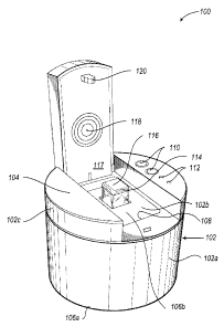
The sampling device 100 includes a housing 102 which, in the
illustrated embodiment, includes a tubular (e.g., cylindrical) main body
housing
portion 102a, a sample chamber 102b in the main body housing portion 102a, and
12
CA 02823481 2013-08-07
a cap 102c having a top surface 104. The housing 102 may, for example, be
sized
and dimensioned as a portable tabletop unit that can be hand carried from one
location to another. Furthermore, such a table top unit is intended to be
accessible
and affordable to a wider range of users than are existing laboratory-based
models.
The main housing portion 102a has a housing base 106a and a
housing top 106b opposite the housing base 106a. The main housing portion
102a has a side wall 108 surrounding the sample chamber 102b which is adjacent
to an exterior surface of the main housing portion 102a. The top end 106b can
be
exposed by opening exemplary hinged lid 117 to provide selective access to the
sample chamber 102b. The main housing portion 102a may be comprised of any
of a large variety of materials, for example ABS plastic, other plastics,
metals (e.g.,
aluminum) and/or composite materials (e.g., carbon fiber impregnated resin).
The
main body housing portion 102a may be sized and dimensioned to be easily held
and operated by a person using a single hand. While illustrated as a cylinder,
the
main body housing portion 102a may take any variety of shapes.
The sampling device 100 may also include one or more function
buttons 110 which are operable from an exterior of the sampling device 100,
for
example, from the cap 102c. The function buttons 110 may take any of a large
variety of forms, other than push-buttons, (e.g., slideable switches,
rotateable
selectors, and the like). For example, a contact or slideable switch may be
actuatable via a window, slot or other aperture in the housing 102.
Additionally or
alternatively, a touch sensitive switch may be employed, for instance an
inductive
or a capacitive switch. The function buttons 110 may be responsive to
actuation to
send a signal, or otherwise cause the sampling device to execute a sampling
operation. As discussed in detail below, the sampling operation may be
preceded
by a calibration operation.
The sampling device 100 may further include one or more visual
indicators (e.g., light emitting diodes or LEDs, two shown collectively
referenced as
13
CA 02823481 2013-08-07
112), shown in Figures 1,2 as located on an upper surface 104 of the cap 102c.
The visual indicators 112 may indicate a status or mode of the sampling device
(e.g., "ready" or "power on"), for instance via different colors (e.g., green,
red,
amber) and or patterns (e.g., flashes). Or, one or more light communicative
paths
(e.g., optical fiber or light pipes) may communicatively couple light to the
visual
indicators 112. Additionally or alternatively, visual indicators 112 may be
located
anywhere on the housing 102, or underneatha window (not shown) mounted
anywhere on the surface of the housing 102.
The sample chamber 102b is sized and dimensioned to at least
partially receive, as shown in Figure 1, a specimen container referred to as a
sample cuvette 114. The sample cuvette 114 may be made of any of a large
variety of materials transmissive (i.e., transparent or at least translucent)
to at least
those wavelengths of electromagnetic energy (e.g., UV) which are used in the
analysis or evaluation of a sample or specimen. Such materials may include,
for
example, silica (i.e., fused quartz) or a cyclic polyolefin commercially
available
from Zeon Chemicals of Louisville, Kentucky under the trademark Zeonex , for
example having minimal absorption characteristics for wavelengths between
approximately 330 nm and extending to or beyond approximately 1,200 nm.
Material transparency may vary with the choice of wavelengths used for
illumination. In addition, containment of different fluids may require
different
materials. A plurality of different cuvette types may therefore be
accommodated
by the sampling device 100. While illustrated as a square cylindrical tube,
the
sample cuvette 114 and sample chamber 102b may take any variety of shapes.
An advantage of the square cylindrical tube is the avoidance of focusing,
refracting, or diffracting certain electromagnetic wavelengths. The sampling
device
100 can further include a port providing flow through fluid communication with
the
sample cuvette 114.
The sample cuvette 114 has a removable cuvette lid 116 that
14
CA 02823481 2013-08-07
need not be transparent. The cuvette lid 116 is desirably made of, or includes
a
material such as rubber, silicone, or another similar elastic material. The
cuvette
lid 116 can thus be capable of forming a seal against the sample cuvette 114
to
prevent leakage of the fluid sample.
The cap 102c can also include an access panel such as a hinged lid
117 that opens to allow access for an operator to load the sample cuvette 114
into
the sample chamber 102b. Alternatively, the access panel could take the form
of a
sliding cover, a fully removable cover, or any number of other lid designs.
The exemplary hinged lid 117 is shown in Figure 1 in an open
position, and in Figure 2 in a closed position. The hinged lid 117 can include
a
stabilizing feature 118 that helps to hold the sample cuvette 114 in a fixed
position.
The hinged lid 117 can further include a latch 120 that holds the hinged lid
117
securely closed during a sample analysis run. The securing engagement may be
selectively releasable under a moderate application of pulling force or
tension on
the hinged lid 117. Additionally or alternatively, the hinged lid 117 can be
released
by an operator action such as, for example, pressing one or both of the
function
buttons 110.
As shown in Figure 2, a finger indentation 200 can be provided in the
top surface of the hinged lid 117 to facilitate selective opening and/or
secure
closure by applying pressure directly over the latch 120. The hinged lid 117
can
be coupled to the sample cuvette 114 such that when the hinged lid 117 is
closed,
the sample cuvette 114 is held down in a fixed position within the sample
chamber
102b. When the hinged lid 117 is in an open position, the sample cuvette 114
can
be automatically released by a biasing member (e.g., spring) so that the
sample
cuvette 114 pops up out of the sample chamber 102b for ease of removal. While
Figures 1 and 2 indicate certain shapes and/or dimensions (e.g., a cylindrical
housing) which may be suitable for some embodiments, the sampling device 100
may employ other shapes and/or dimensions. Thus, the specified shapes and/or
dimensions should not be considered limiting. Figure 3 presents a view 300 of
the
CA 02823481 2013-08-07
housing cap 102c, showing a pair of hinges 302 about which the hinged lid 117
pivots. In one embodiment, the hinges 302 are located near the perimeter of
the
cap 102c. It is noted that any number of alternative lid configurations can be
substituted for the hinged lid 117 shown.
Figure 4 depicts a view 400 of the housing 102, showing a plurality of
feet 402a, 402b, 402c, and 402d, (four shown, collectively 402) on which the
sampling device 100 can rest on a table top or desk top, for example. Also
shown
in Figure 4 is a pair of screws 404a and 404b (two shown, collectively 404)
and a
drain hole 406. The drain hole 406 can prevent any liquid that may escape both
the sample cuvette 114 and the sample chamber 102b from accumulating inside
the housing 102.
Figure 5 shows a view 500 of the back of the sampling device 100, in
which is shown a panel 502 surrounding a cable receptacle 504. The panel 502
may be a removable access panel. While the cable receptacle 504 is pictured as
a
USB port it is not so limited. One or more other types of communications ports
and/or power supply connections, or combinations thereof, may be provided in
conjunction with the panel 502. Such connections may provide pathways for
power delivery and uni-directional or bi-directional data flow to support the
functions of the sampling device 100. Alternatively, or in addition, power
and/or
data connections to the sampling device 100 can be partly or fully wireless,
thereby allowing data upload to a Web site via the Internet, for example.
Instructions may also be received by the sampling device via the cable
receptacle
504 or via a wireless connection.
Figure 6 shows a view 600 of internal parts within the sampling
device 100 relative to the sample cuvette 114. In the center is shown the top
surface of the cuvette lid 116. Inside the illustrated sampling device 100 are
shown four printed circuit board assemblies (PCBAs): a transducer PCBA 602, a
calibrator PCBA 604, a direct sensor PCBA 606, and a backplane PCBA 608,
which also serves as an indirect sensor PCBA. In the embodiment shown, the
16
CA 02823481 2013-08-07
PCBAs 602, 604, and 606 are oriented substantially parallel to one another and
substantially perpendicular to the backplane PCBA 608, to which they connect.
This orientation of the PCBAs provides a rigid structure that helps to direct
the
electromagnetic energy path. As illustrated, the backplane PCBA 608 may be
sized and dimensioned to be securely received in housing 102, for example
engaging an inner periphery of the housing base 106a, an inner periphery of
the
side wall 108, or other attachment structures. Engagement may be via a press
fit
or via some coupling structure such as a detent structure, or a clip as shown
below
in Figure 12 to secure the PCBAs 602, 604, and 606.
The PCBAs 602, 604, 606, and 608 may comprise any of a large
variety of materials, for example plastics metals, or composite materials. The
PCBAs are typically opaque or substantially opaque, at least to
electromagnetic
energy that is employed in the analysis or evaluation of the samples or
specimens.
The PCBAs may, for example, be painted black, coated black, or may include
black pigments.
According to one embodiment, the function buttons 110 and visual
indicators 112 are shown mounted to the top of the transducer PCBA 602. The
function buttons 110 are further shown attached to function button support
plates
610 via function button fasteners 612. The function button support plates 610
are
coupled to the transducer PCBA 602 by function button coupling pins 614 that
are
through-hole mounted to the transducer PCBA 602. Electrical connections from
the function buttons 110 are also coupled to internal electronic and/or
electrical
components via the transducer PCBA 602. Similarly, the visual indicators 112
are
attached to indicator support plates 616, and the indicator support plates 616
are
coupled to the transducer PCBA 602 via indicator coupling pins 618. Other form
factors for the function buttons 110, visual indicators 112, and associated
connections, or an alternative user interface can be substituted for those
shown.
As explained in more detail below, the transducer PCBA 602
includes a plurality of transducers, typically in the form of a plurality of
emitters
17
CA 02823481 2013-08-07
(seven shown, collectively 634). The calibrator PCBA 604 includes one or more
calibration detectors or sensors (four shown, collectively 636). The direct
sensor
PCBA 606 includes one or more first primary sampling detectors or sensors
(four
shown, collectively 638). Also as explained in more detail below, the
backplane
PCBA 608 includes one or more second primary sampling detector(s) or sensor(s)
(four shown, collectively 640), and various other electrical and electronic
components (collectively 642) to control operation of the sampling device 100
and/or communications therefrom. The transducer PCBA 602, the calibrator
PCBA 604, and the direct sensor PCBA 606 each include a respective coupler or
connector 644a, 644b, and 644c, respectively, to communicatively couple
electronic and/or electrical components or circuits of the each of the PCBAs
602,
604, and 606 with the components or circuits of the backplane PCBA 608.
Accordingly, the backplane PCBA 608 can be configured with a plurality of
sockets
for receiving the connectors 644a, 644b, and 644c. Connectors 644a, 644b, and
644c may be slot connectors having a slot sized and dimensioned to mate with a
coupler of the transducer PCBA 602, for instance an edge or tab. Each of the
couplers or connectors 644a, 644b, and 644c typically carry a variety of
electrical
contacts, although other signal transfer structures (e.g., optical fiber) can
be
employed.
Power can also be supplied to each of the PCBAs 602, 604, and 606
through the connectors 644a, 644b, and 644c. A power source (not shown) may
take the form of a portable power source, for example one or more batteries,
fuel
cells, and/or super- or ultra-capacitors. Additionally, or alternatively, the
power
source may take the form of a fixed power source, such as a cable plugged into
a
port of a computer (e.g., USB cable) or a conventional electrical receptacle
(e.g.,
wall outlet).
The backplane PCBA 608 may, for example, optionally include a
control subsystem 646 implemented as one or more integrated circuit chips
attached to the PCBA 608. Alternatively, the sampling device 100 may be
coupled
18
CA 02823481 2013-08-07
to an external control system, for example one or more programmed general
purpose or special purpose computers or computer systems.
The control subsystem 646 may, for example, be coupled to a central
communications port 647 (e.g., Universal Serial Bus (USB) or mini-USB
compliant
female connector) as shown in Figure 6. The central communications port 647
may be accessible from the exterior of the housing 102, for example via the
cable
receptacle 504 and the removable access panel 502 in the surface of the
housing
102. While illustrated as a hardwired communication port 647 (e.g., a USB
port),
the sampling device 100 may include other types of communications ports or
devices, for instance an infrared transceiver, or an RF transceiver (e.g.,
BLUETOOTH transceiver). Such may allow the transmission of data, instructions
and/or results, to or from the sampling device 100.
The control subsystem 646 may also include one or more controllers
648, for example, one or more microprocessors, digital signal processors
(DSPs),
application specific integrated circuits (ASICs), programmable gate arrays
(PGA),
programmable logic controllers (PLCs), or other logic executing device. The
control subsystem may include one or more non-transitory computer- or
processor-
readable media, for example one or more memories 650 such as read only
memory (ROM) 650a, or Flash memory 650b and random access memory (RAM)
650c. One or more buses (not shown) may couple the ROM 650a and RAM 650c
to the controller 648. The buses may take a variety of forms including an
instruction bus, data bus, other communications bus and/or power bus. A
nonvolatile ROM and/or Flash memory 650b may store instructions and/or data
for
controlling the sampling device 100. The volatile RAM 650c may store
instructions
and/or data for use during operation of the sampling device 100.
The optional controller 648 can employ instructions and or data from
the ROM/Flash 650b and RAM 650c in controlling operation of the sampling
device
100. For example, the controller 648 operates the emitters 634 in one or more
sequences. The sequences determine an order in which the emitters 634 are
19
CA 02823481 2013-08-07
turned ON and OFF. The sequences may also indicate an ordered pattern of drive
levels (e.g., current levels, voltage levels, duty cycles) for the emitters
634. Thus,
for example, a controller 648 may cause the application of different drive
levels to
respective ones of the emitters 634 to cause the emitters 634 to emit in
distinct
bands of the electromagnetic spectrum. Thus, the ranges of wavelengths of some
of the emitters can be different from the ranges of wavelengths of others of
the
emitters.
The controller 648 may process information generated by the primary
sampling detector(s) or sensor(s) 638, 640, which is indicative of the
response by
at least a portion of a sample or specimen to illumination by the emitters
634. The
information at any given time may be indicative of the response by the sample
or
specimen to illumination by one or more of the emitters 634. Thus, the
information
over a period of time may be indicative of the responses by the sample or
specimen to sequential illumination by each of a plurality of the emitters
634,
where each of the emission spectra of each of the emitters 634 has a different
center, bandwidth and/or other more complex differences in spectral content,
such
as those described above (e.g., width of the band, the skew of the
distribution, the
kurtosis, etc.). The control subsystem 646 may optionally include a buffer
(not
shown) to buffer information received from the primary sampling detector(s) or
sensor(s). The control subsystem 646 may further optionally include an analog
to
digital converter (ADC) (not shown) and/or digital to analog converter (DAC)
(not
shown). An ADC may, for example, be used for converting analog photodiode
responses into digital data for further analysis and/or transmission. A DAC
may,
for example, be used for converting digital computer or controller commands
into
analog LED current levels. The control subsystem may additionally or
alternatively
optionally include an analog signal processor, which may be particularly
useful
where the sensor takes the form of one or more photodiodes.
The control subsystem 646 may include a user interface including
one or more user interface devices. For example, the control subsystem 646 may
CA 02823481 2013-08-07
include one or more speakers or microphones (not shown). Also for example, the
control subsystem 646 may include and/or one or more visual indicators, such
as
one or more LEDs, liquid crystal displays (LCD), or other visual indicators,
which
could include visual indicators 112. The LCD may, for example, take the form
of a
touch sensitive LCD, which displays a graphical user interface, operable by
the
user of the sampling device 100.
Additionally, or alternatively, the control subsystem 646 may include
one or more user operable input elements, such as switches, keys or buttons,
which may include the function buttons 110. The input elements may include a
switch for turning the sampling device 100 ON and OFF. Additionally, or
alternatively, the input elements may include one or more switches or keys for
controlling operation of a test device that can, for example, download or
upload
data or instructions to, or from the sampling device 100.
Figure 7 shows a view 700 of the interior parts shown in Figure 6,
relative to the cap 102c and to the sample chamber 102b. Figure 7 also shows,
from above the sampling device 100, the system geometry, including locations
of
the emitters 634 and the primary sampling detectors or sensors 638 and 640.
Figure 7 further includes a ray drawing superimposed onto the view
700, in which arrows indicate transmission paths of electromagnetic energy
relative to the interior parts of the sampling device 100. In one embodiment,
emitters 634 are selectively operable to emit electromagnetic energy in a
respective range of wavelengths through an emission angle that is
substantially
centered on an optical axis 702. The electromagnetic energy is generally
blocked
by the calibrator PCBA 604 except where the energy is transmitted through a
PCBA slit 704 in the calibrator PCBA 604. The PCBA slit 704 can be
substantially
aligned with one or more of the emitters 634. Electromagnetic waves admitted
through the PCBA slit 704 continue to propagate toward and through a first
aperture 706 of the sample chamber 102b and through the transparent walls of
the
sample cuvette 114. A second aperture 708 of the sample chamber 102b is
21
CA 02823481 2013-08-07
positioned at least partially across at least a portion of the sample chamber
102b
from the first aperture 706. A third aperture 710 of the sample chamber 102b
is
positioned at least partially across at least a portion of the sample chamber
102b
from both the first and the second apertures 706 and 708, respectively. The
first,
second, and third apertures, 706, 708, and 710 are transmissive of
electromagnetic energy of at least some wavelengths in an optical portion of
the
electromagnetic spectrum, as is the sample cuvette 114.
As the ray drawing indicates, electromagnetic energy strikes the
sample or specimen and is scattered and/or reflected therefrom. The scattered
electromagnetic waves then emerge from the at least partially transparent
walls of
the sample cuvette 114, propagating outward in various directions. Again, the
electromagnetic energy is generally blocked by the walls of the sample chamber
102b, except where the second aperture 708 permits transmission in the forward
scattering direction, along the optical axis 702. The third aperture 710
permits
transmission of the scattered energy in a direction perpendicular to the
optical axis
702, along a perpendicular axis 703.
After passing through the second aperture 708, a portion of scattered
electromagnetic energy propagating along the optical axis 702 falls incident
on,
and thus can be detected by the first primary sampling detector(s) or
sensor(s) 638
mounted on the direct sensor PCBA 606. Similarly, after passing through the
third
aperture 710, a portion of scattered electromagnetic energy propagating along
the
perpendicular axis 703 can be detected at one or more of the second primary
sampling detector(s) or sensor(s) 640 mounted on the direct sensor PCBA (also
the backplane PCBA) 608. In some applications, time varying processes, for
example, chemical or biological reactions, can be monitored by detecting the
onset
of, or change(s) in, "side scatter" along the perndicular axis 703. Onset of
such
side scatter can indicate, for example, formation of crystals, bacterial
growth,
formation of blood clots, or other substances in a fluid that can cause
electromagnetic energy to be scattered in the direction of the second primary
22
CA 02823481 2013-08-07
sampling detector(s) or sensor(s) 640. Commensurate with an increase in side
scatter along the perpendicular axis 703, there may be observed a decrease in
transmission of electromagnetic energy along the optical axis 702. In some
instances, such a decrease in transmission intensity and an increase in side
scatter intensity can be observed substantially simultaneously (i.e.,
concurrently)
using the sampling device 100. The ability to detect such changes represents a
feature of the sampling device 100 that is not provided by other types of
sampling
devices.
Figure 8 shows a view 800 of the sample chamber 102b. The
sample chamber 102b receives and protects the sample cuvette 114 containing
the fluid sample under test. The sample cuvette 114 can be inserted at least
partially into the center of the sample chamber 102b, which fits closely
around the
sample cuvette 114. In one embodiment, the sample chamber 102b can be raised
and lowered during loading of the sample cuvette. The sample chamber 102b can
serve as a double containment receptacle to prevent liquids that may escape
the
sample cuvette 114 from coming into contact with electronic components of the
sampling device 100. The sample chamber 102b can feature a plurality of
apertures described above, e.g., the first aperture 706, the second aperture
708,
and the third aperture 710, to allow electromagnetic energy to be transmitted
to
and scattered (or re-emitted) from a sample within the sample cuvette 114. In
this
way, the sample chamber 102b guides light into the sample cuvette 114.
Otherwise, the walls of the sample chamber can be opaque, such that the sample
chamber 102b has at least one opaque wall. The first aperture 706 in the
sample
chamber 102b allows passage of incident electromagnetic energy from one or
more of the emitters 634, along the optical axis 702, and through the sample
cuvette 114 to interact with the fluid sample. In one embodiment, the second
aperture 708 is diametrically opposed to the first aperture 706, allowing
passage of
scattered electromagnetic energy in the forward direction to exit the sample
chamber 102b for detection. The third aperture 710 is disposed along a second
23
CA 02823481 2013-08-07
axis 703, non-collinear with the optical axis 702. In the embodiment shown,
the
second axis 703 and the third aperture 710 are oriented perpendicular to the
optical axis 702. As illustrated, the first aperture 706 is shown larger than
the third
aperture 710. However, the relative dimensions of the apertures 706, 708, and
710 can change depending on the type of emitters 634, the nature of the
sample,
and other variables.
Figure 9 shows a view 900 of the PCBAs 602, 604, 606, and 608,
relative to the sample cuvette 114, in which the calibration sensors 636 and
the
primary sampling detector(s) or sensor(s) 638, 640 are visible. In an
exemplary
embodiment, the PCBAs 602, 604, 606, and 608 can attach to the housing 102 by
fitting notches 902 onto clips 904 (see Figure 12). The clips 904 can, in
turn, be
secured to an interior surface of the base of the housing 106a. When mounted
in
front of the transducer PCBA 602, the calibrator PCBA 604 serves as a mask in
which the PCBA slit 704 allows electromagnetic energy to reach and interact
with
the fluid sample. The transparent sample cuvette 114 allows electromagnetic
energy scattered from the fluid sample to reach the primary sampling
detector(s) or
sensor(s) 638.
As is best illustrated in Figure 9, the transducer PCBA 602 carries a
number of emitters or sources 634 arranged, for example, in a linear array on
the
transducer PCBA 602. The emitters 634 may be all aligned with the PCBA slit
704
and the first aperture 706. A full range of emitters can include, for example,
5 - 10
emitter chips in which each emitter can be made to produce a range of
wavelengths of light depending on the electric current supplied to it.
Respective
ranges of emitters can overlap such that a full range of desired wavelengths
can
be produced by driving a few emitters at many different current levels. The
emitters 634 may take a variety of forms which are operable to emit
electromagnetic energy. The emitters 634 may, for example, take the form of
one
or more light emitting diodes (LEDs), including for instance organic LEDs
(OLEDs).
Alternatively, or additionally, the emitters 634 may take the form of one or
more
24
CA 02823481 2013-08-07
lasers, for example one or more laser diodes. The lasers may, or may not, be
tunable lasers. Alternatively, or additionally, the emitters 634 may take the
form of
one or more incandescent sources such as conventional or halogen light bulbs.
One, more, or all of the emitters 634 may be operable to emit in part
or all of an "optical" portion of the electromagnetic spectrum, including the
(human)
visible portion, near infrared (N-IR) portion and/or or near ultraviolet (N-
UV)
portions of the electromagnetic spectrum. Additionally, or alternatively, the
emitters 634 may be operable to emit electromagnetic energy other portions of
the
electromagnetic spectrum, for example the infrared, ultraviolet and/or
microwave
portions.
In some embodiments, at least some of the emitters 634 are
operable to emit in or at a different band than other of the emitters 634. For
example, one or more emitters 634 may emit in a band centered around 450 nm,
while one or more of the emitters 634 may emit in a band centered around 500
nm,
while a further emitter or emitters emit in a band centered around 550 nm.
Each of
the emitters 634 may emit in a band centered around a respective frequency or
wavelength, different than each of the other emitters 634. Using emitters 634
with
different band centers advantageously maximizes the number of distinct samples
that may be captured from a fixed number of emitters 634. This may be
particularly advantageous where the sampling device 100 is relatively small,
and
has limited space or footprint for the emitters 634.
The distribution of spectral content for each emitter 634 may vary as
a function of drive level (e.g., current, voltage, duty cycle), temperature,
and other
environmental factors, depending on the specific emitter 634. Such variation
may
be advantageously actively employed to operate one or more of the physical
emitters 634 as a plurality of "logical emitters or sources," each of the
logical
emitters or sources operable to provide a respective emission spectra from a
respective physical emitters or source 634. Thus, for example, the center of
the
band of emission for each emitters or source 634 may vary according to a drive
CA 02823481 2013-08-07
level and/or temperature. For example, the center of the band of emission for
LEDs will vary with drive current or temperature. One way the spectral content
can
vary is that the peak wavelength can shift. However, the width of the band,
the
skew of the distribution, the kurtosis, etc., can also vary. Such variations
may be
also be advantageously employed to operate the physical emitters or sources
634
as a plurality of logical emitters or sources. Thus, even if the peak
wavelength
were to remain constant, the changes in bandwidth, skew, kurtosis, and any
other
change in the spectrum can provide useful variations in the operation of the
sampling device 100. Likewise, the center of the band of emission may be
varied
for tunable lasers. Varying the center of emission bands for one or more
emitters
634 advantageously maximizes the number of samples that may be captured from
a fixed number of emitters 634. Again, this may be particularly advantageous
where the sampling device 100 is relatively small, and has limited space or
footprint for the emitters 634.
As is best illustrated in Figure 10, the calibration PCBA 604 carries a
number of calibration detectors or sensors (four shown, collectively 636),
arranged
around the PCBA slit 704. The number of calibration detectors or sensors 636
can
correspond to the number of emitters 634. The calibration detectors or sensors
636 are generally aligned with respective emitters 634, the calibration
detectors or
sensors 636 and emitters 634 for example being arranged in linear segments on
a
surface of the calibration PCBA 604. The calibration detectors or sensors 636
may
match a nominal output of the respective emitter 634 to which the calibration
detector or sensor 636 is paired. Thus, some of the calibration detectors or
sensors 636 may be responsive to different respective bands of wavelengths
than
the others. Such bands may be mutually exclusive or may be overlapping. Some
embodiments employ one or more wideband calibration detectors or sensors 636,
for example, a pyroelectric detector from Pyreos Ltd. Such may advantageously
reduce parts counts, while still allowing calibration across the range of
wavelengths of the emitters 634. Optionally, one or more filters (not shown)
may
26
CA 02823481 2013-08-07
be employed with the calibration detectors or sensors 636, for example one or
more low pass filters, high pass filters, and/or band pass filters. The
filters may be
optical filters and may be formed or carried directly on the calibration
detectors or
sensors 636. Alternatively, the filters may be formed on or carried on another
surface, in the field of view of but spaced from the calibration detectors or
sensors
636.
The calibration detector(s) or sensor(s) 636 can take a variety of
forms suitable for sensing or responding to electromagnetic energy. For
example,
the calibration detector(s) or sensor(s) 636 may take the form of one or more
photodiodes (e.g., germanium photodiodes, silicon photodiodes). Alternatively,
or
additionally, the calibration detector(s) or sensor(s) 636 may take the form
of one
or more photomultiplier tubes. Alternatively, or additionally, the calibration
detector(s) or sensor(s) 636 may take the form of one or more CMOS image
sensors. Alternatively, or additionally, the calibration detector(s) or
sensor(s) 636
may take the form of one or more charge coupled devices (CCDs). Alternatively,
or additionally the calibration detector(s) or sensor(s) 636 may take the form
of one
or more micro-channel plates. Other forms of electromagnetic sensors may be
employed, which are suitable to detect the wavelengths expected to be returned
in
response to the particular illumination and properties of the object being
illuminated.
The calibration detector(s) or sensor(s) 636 may be formed as
individual elements, one-dimensional array of elements and/or two-dimensional
array of elements. For example, the calibration detector(s) or sensor(s) 636
may
be formed by one germanium photodiode and one silicon photodiode, each having
differing spectral sensitivities. A test device may employ a number of
photodiodes
with identical spectral sensitivities, with different colored filters (e.g.,
gel filters,
dichroic filters, thin-film filters, etc) over the photodiodes to change their
spectral
sensitivity. This may provide a simple, low-cost approach for creating a set
of
sensors with different spectral sensitivities, particularly since germanium
27
CA 02823481 2013-08-07
photodiodes are currently significantly more expensive that silicon
photodiodes.
Also for example, the calibration detector(s) or sensor(s) 636 may be formed
from
one CCD array (one-dimensional or two-dimensional) and one or more
photodiodes (e.g., germanium photodiodes and/or silicon photodiodes). For
example, the calibration detector(s) or sensor(s) 636 may be formed as a one-
or
two-dimensional array of photodiodes. A two-dimensional array of photodiodes
enables very fast capture rate (i.e., camera speed) and may be particularly
suited
to use in assembly lines or high speed sorting operations. For example, the
calibration detector(s) or sensor(s) 636 may be formed as a one- or two-
dimensional array of photomultipliers. Combinations of the above elements may
also be employed.
In some embodiments, the calibration detector(s) or sensor(s) 636
may be a broadband sensor sensitive or responsive over a broad band of
wavelengths of electromagnetic energy. In some embodiments, the calibration
detector(s) or sensor(s) 636 may be narrowband sensors sensitive or responsive
over a narrow band of wavelengths of electromagnetic energy. In some
embodiments, the calibration detector(s) or sensor(s) 636 may take the form of
several sensor elements, as least some of the sensor elements sensitive or
responsive to one narrow band of wavelengths, while other sensor elements are
sensitive or responsive to a different narrow band of wavelengths. This
approach
may advantageously increase the number of samples that may be acquired using
a fixed number of sources. In such embodiments the narrow bands may, or may
not, overlap.
As is best illustrated in Figure 11, the direct sensor PCBA 606 carries
a number of first primary sampling sensors 638a-638d (four shown, collectively
638) positioned opposite the PCBA slit 704. The first primary sampling sensors
638 may, for example, include two or more sampling sensors or detectors, each
responsive to a respective band of wavelengths. Such bands may be mutually
exclusive or overlapping. The illustrated embodiment employs four first
primary
28
CA 02823481 2013-08-07
sampling detectors or sensors 638a-638d, each responsive to a respective band
of
wavelengths (i.e., 400nm-1100nm, 400nm-1050nm, 400nm-1050nm, 600nm-1700
nm, respectively). Three of the first primary sampling detectors or sensors
638a-
638c that are responsive to N-UV wavelengths are employed to increase to
sensitivity. Another embodiment employs one or more wideband first primary
sampling detector(s) or sensor(s) 638d, for example, a pyroelectric detector
from
Pyreos Ltd. Optionally, one or more filters (not shown) may be employed with
the
first primary sampling detector(s) or sensor(s) 638, for example one or more
low
pass filters, high pass filters, and/or band pass filters. The filters may be
optical
filters and may be formed or carried directly on the first primary sampling
detector(s) or sensor(s). Alternatively, the filters may be formed on or
carried on
another surface, in the field of view of but spaced from the first primary
sampling
sampling detector(s) or sensor(s) 638.
The first primary sampling detector(s) or sensor(s) 638, or
spectrophotometers, can take a variety of forms suitable for sensing or
responding
to electromagnetic energy. For example, the primary sampling sensor(s) 638 may
take the form of one or more photodiodes (e.g., germanium photodiodes, silicon
photodiodes). Alternatively, or additionally, the primary sampling detector(s)
or
sensor(s) 638 may take the form of one or more photomultiplier tubes.
Alternatively, or additionally, the first primary sampling detector(s) or
sensor(s) 638
may take the form of one or more CMOS image sensors. Alternatively, or
additionally, the first primary sampling detector(s) or sensor(s) 638 may take
the
form of one or more charge coupled devices (CODs). Alternatively, or
additionally
the first primary sampling detector(s) or sensor(s) 638 may take the form of
one or
more micro-channel plates. Other forms of electromagnetic sensors may be
employed, which are suitable to detect the wavelengths expected to be returned
in
response to the particular illumination and properties of the object being
illuminated.
29
CA 02823481 2013-08-07
The first primary sampling detector(s) or sensor(s) 638 may be
formed as individual elements, one-dimensional array of elements and/or two-
dimensional array of elements. For example, the first primary sampling
detector(s)
or sensor(s) 638 may be formed by one germanium photodiode and one silicon
photodiode, each having differing spectral sensitivities. A test device can be
configured with a number of photodiodes having identical spectral
sensitivities,
with different colored filters (e.g., gel filters, dichroic filters, thin-film
filters, etc.)
over the photodiodes to change their spectral sensitivity. This may provide a
simple, low-cost approach for creating a set of sensors with different
spectral
sensitivities, particularly since germanium photodiodes are currently
significantly
more expensive that silicon photodiodes. Also for example, the first primary
sampling detector(s) or sensor(s) 638 may be formed from one CCD array (one-
dimensional or two-dimensional) and one or more photodiodes (e.g., germanium
photodiodes and/or silicon photodiodes). For example, the first primary
sampling
detector(s) or sensor(s) 638 may be formed as a one- or two-dimensional array
of
photodiodes. A two-dimensional array of photodiodes enables very fast capture
rate (i.e., camera speed) and may be particularly suited to use in assembly
lines or
high speed sorting operations. For example, the first primary sampling
detector(s)
or sensor(s) 638 may be formed as a one- or two-dimensional array of
photomultipliers. Combinations of the above elements may also be employed.
In some embodiments, the primary sampling detector(s) or sensor(s)
638, 640 may be a broadband sensor sensitive or responsive over a broad band
of
wavelengths of electromagnetic energy. In some embodiments, the primary
sampling detector(s) or sensor(s) 638, 640 may be narrowband sensors sensitive
or responsive over a narrow band of wavelengths of electromagnetic energy. In
some embodiments, the primary sampling detector(s) or sensor(s) 638, 640 may
take the form of several sensor elements, as least some of the sensor elements
sensitive or responsive to one narrow band of wavelengths, while other sensor
elements are sensitive or responsive to a different narrow band of
wavelengths.
CA 02823481 2013-08-07
This approach may advantageously increase the number of samples that may be
acquired using a fixed number of sources. In such embodiments the narrow bands
may, or may not, overlap.
At least one of the PCBAs 602, 604, 606, and 608 can also carry one
or more thermal sensors (not explicitly shown). The thermal sensors are
desirably
distributed to detect temperature at a variety of points or locations. Such
temperatures may be indicative of temperatures to which the emitters 634,
first
primary sampling detectors or sensors 638 and/or calibration detectors or
sensors
636 are subjected. Temperature indicative signals from the thermal sensors may
be employed in calibration, for example, calibrating results or responses
and/or
calibrating drive signals to account from variation from nominal temperatures
or
other conditions.
Table A, below, provides an exemplary list of suitable parts for the
emitters and sensors. Such is purely illustrative and is not intended to
require any
specific parts, specific wavelengths, or sensitivities.
Table A
Ref. No. Part No. Description Default/ Qty.
606 Max2 Sensor PCBA PCBA 1
MCP98242 Thermal Sensor 4
644a HSEC8-120-01-X-DV Connector 1
634a 350-PLCC2-120 352nm 1
634b SM1206UV-395-IL 400nm 1
634c EL-19-21/BHC-AN1P2/3T 468nm 1
634d PG1112C-TR 567nm 1
634e LTST-C190KYKT 595 nm 1
634f SMC810 810 nm 1
634g SMC1200 1200 nm 1
634h LNJ812R83RA 630 nm 1
6341 SMC1450 1450 nm 1
634j SMC910 910 nm 1
634k LN1251CTR 700 nm 1
31
CA 02823481 2013-08-07
Ref. No. Part No. Description Default/ Qty.
6341 SMC970 970 nm 1
636a PDB-C152SM 400-1100 nm 1
636b SFH2701 400-1050 nm 1
636c PDB-C152SM 400-1100 nm 1
636d LAPD-1-06-17-LCC 600-1700 nm 1
638a SFH2701 400-1050 nm 1
638b SFH2701 400-1050 nm 1
638c PDB-C152SM 400-1100 nm 1
638d PDB-C152SM 400-1100 nm 1
638e PDB-C152SM 400-1100 nm 1
638f PDB-C152SM 400-1100 nm 1
6389 LAPD-1-06-17-LCC 600-1700 nm 1
638h PDB-C152SM 400-1100 nm 1
638i LAPD-1-06-17-LCC 600-1700 nm 1
638j PDB-C152SM 400-1100 nm 1
638k PDB-C152SM 400-1100 nm 1
6381 PDB-C152SM 400-1100 nm 1
By commonly housing emitters 634 with respective calibration
detector(s) or sensor(s) 636 or sensors 638, the sampling device may
automatically take or capture an electromagnetic energy calibration sample or
measurement each time an emitter emits electromagnetic energy. Such is
performed in real-time, without any separate calibration mode. Such may be
performed individually for each emitter, one at a time, as the emitter is
activated.
Thermal sensors 635 may be sampled each time an emitter is activated.
Alternatively, the thermal sensors 635 may be sampled periodically or
aperiodically. The electromagnetic energy calibration sample or measurements
and thermal calibration sample or measurements may be used to calibrate a
detected or measured response. The electromagnetic energy calibration sample
or measurements and thermal calibration sample or measurements may
32
CA 02823481 2013-08-07
additionally or alternatively be used to control operation, for instance to
control a
drive signal supplied to the emitters, or control an amplification applied to
a signal
produced or provided by the first primary sampling detectors or sensors 638.
As
discussed below, the electromagnetic energy calibration sample or measurements
and thermal calibration sample or measurements may be processed on the
sampling device 100, or sent to a separate component (e.g., digital computer)
for
processing.
While Figures 9-11 show seven emitters 634, four calibration
detector(s) or sensor(s) 636 and eight primary sampling detectors or sensors
638,
640, other embodiments may include fewer or greater number of emitters 634,
and
calibration detector(s) or sensor(s) 636 or primary sampling detector(s) or
sensor(s) 638, 640. The total number of emitters 634, calibration detector(s)
or
sensor(s) 636, and primary sampling detector(s) or sensor(s) 638, 640, should
not
be considered limiting.
Figure 12 shows a view 1200 of the sampling device 100 as seen
from the rear. Internal parts are shown relative to overall structural
components
such as the main body housing portion 102a, the cap 102c, the hinged lid 117,
and
the sample chamber 102b. Superimposed onto the structure of the sampling
device 100 is a side view of a ray diagram similar to that shown in Figure 7.
In the
view 1200, electromagnetic energy is shown being emitted through a wide range
of
angles from the exemplary top and bottom emitters 634a and 634g. The diameter
of the emitted beam may depend on the nature of the emitter. The outermost
rays
1202a and 1202g, emanating from the emitters 634a and 634g, respectively, fail
to
pass through the PCBA slit 704 (not shown) and therefore do not interact with
the
sample. If the emitters 634 are laser sources, for example, the outermost rays
may not be relevant because laser sources produce a collimated beam.
(However, even a collimated beam may exhibit spreading.) In general, a portion
of
the energy emitted can be expected to escape the system without encountering
the sample under test. The innermost rays emitted, 1204a and 1204g,
33
CA 02823481 2013-08-07
respectively, are shown crossing at the center of the sample cuvette 114, in
front
of the second primary sampling detector(s) or sensor(s) 640, which are
attached to
the backplane 608. The innermost rays therefore interact with substantially
the
same part of the sample contained in the sample cuvette 114. It is noted that
the
innermost rays shown have different wavelengths because they originate at
different sources. A portion of the electromagnetic energy in the innermost
rays
1204a and 1204g is scattered by the sample. Some of the scattered energy is
shown continuing to propagate in the forward direction for detection by the
sensors
638. Thus, comparing the energy scattered by the same sample at multiple
wavelengths permits identification of a localized portion of the sample.
Meanwhile,
the central rays 1206a and 1206g, from the two different emitters 634a and
634g,
respectively, interact with different portions of the fluid sample. The
central rays
are also scattered, and a portion of this scattered energy propagates to the
detectors 638. By comparing the scattered energy from the central rays 1206a
and 1206g with that from the innermost rays 1204a and 1204g, information about
the homogeneity of the sample can be obtained. For example, particles
suspended in the fluid can be identified and distinguished from the fluid
itself.
Figure 13 shows a sampling system 1300, according to one
illustrated embodiment. The sampling system 1300 includes one or more
sampling devices 100 (one shown). The sampling system 1300 includes one or
more processor-based devices 1302 (one shown). While illustrated as a mobile
or
handheld processor-based device 1302, for instance a Smartphone type device,
the processor-based device 1302 may take a large variety of other forms. For
example, the mobile or handheld processor-based device 1302 may take the form
of the various computers or computing systems, such as a desktop or laptop
personal computer, tablet computer, netbook computer, mini-computer, mainframe
computer, or server computer.
The sampling device 100 is communicatively coupled to the
processor-based device 1302.
34
CA 02823481 2013-08-07
The sampling device 100 may be communicatively coupled to the
processor-based device 1302 via a physical communicative path such as a cable
1304.
The cable 1304 will typically include a connector proximate at least
one end thereof, and often at both ends. For example, the cable 1304 may have
a
first connector 1304a (e.g., plug) at a first end 1306a, the first connector
1304a
selectively detachably coupleable to a complimentary connector or port 1308 on
the processor-based device 1302. Also for example, the cable 1304 may have a
second connector 1304b (e.g., plug) at a second end 1306b, the second
connector
1304b selectively detachably coupleable to a complimentary connector or port
on
the sampling device 100 such as the cable receptacle 504. Alternatively, the
second end of the cable 1304 may be permanently fixed to the sampling device
100. The physical ports and/or connectors 1304a, 1304b, 1308, 504 and/or
cables
1304 may comply with any variety of physical and/or logical standards, and may
incorporate one or more integrated circuits. For instance, the ports and/or
connectors 1304a, 1304b, 1308, 504 and/or cables 1304 may comply with
standards required of USB standards or Apple Computer's Lighting standards.
The cable 1304 may, for instance, include a number of distinct
electrical conductors (e.g., wires) (not shown) to provide signals between the
sampling device 100 from the processor-based device 1302. The electrical
conductors may provide for bi-directional communications between the sampling
device 100 and the processor-based device 1302. The cable 1304 may
additionally provide electrical power (e.g., 5V, 10V) to the sampling device
100
from the processor-based device 1302. In such an implementation, the sampling
device 100 may omit any on-board consumable power source (e.g., primary or
secondary chemical battery, ultra-capacitor, fuel cell) (not shown).
Alternatively,
the sampling device 100 may include a recharging circuit (not shown) that uses
electrical power supplied via the cable 1304 to recharge an onboard power
source
(e.g., secondary chemical battery, ultra-capacitor, fuel cell) (not shown).
CA 02823481 2013-08-07
The cable 1304 may include one or more optical paths (e.g., optical
fibers) (not shown). The optical paths may provide for bi-directional
communications between the sampling device 100 and the processor-based
device 1302.
The sampling device 100 may be communicatively coupled to the
processor-based device 1302 via a wireless (e.g., radio frequency, microwave,
visible or IR light) communicative path. As discussed below, many processor-
based devices 1302 include various radios or receivers, including ones that
are
compliant with cellular (e.g., CDMA, GSM, LTE), BLUETOOTH or WI-Fl protocols.
In such implementations, the sampling device 100 may include one or more
radios
or transceivers (not shown) can be implemented as one or more integrated
circuits
and/or antennas (not shown). The integrated circuits and/or antennas (not
shown)
may be carried by the backplane PCBA 608 or some other PCBA, for instance a
dedicated communications PCBA (not shown). In such implementations, the
sampling device 100 will typically require an on-board consumable power source
(e.g., primary or secondary chemical battery, ultra-capacitor, fuel cell) (not
shown).
The sampling device 100 may be communicatively coupled via one
or more networks (not shown) to various processor-based devices 1302 and/or
other sampling devices 100. The network(s) may take a variety of forms
including
LANs, WANs, WLANs, VVWANs, PSTN, to name a few. Such may, for example
allow access to one or more storage or databases of information. Such may, for
example allow updating or reconfiguration, for instance by downloading of
processor-executable instructions. Such may, for example, allow
troubleshooting
of the sampling device 100 should an error condition occur.
The processor-based device 1302 may include a user interface
which may, for example include a touch-sensitive display 1312, speakers 1314
(one shown), microphones 1316a, 1316b (collectively 1316), and/or an audio
output port 1318. The user interface may also include user selectable icons,
collectively 1320, and/or one or more physical switches, keys or buttons 1322.
36
CA 02823481 2013-08-07
Figure 13 further illustrates a PCBA 1324 of the processor-based
device 1302, removed therefrom to better illustrate various components housed
within a housing of the processor-based device 1302. The processor-based
device 1302 includes one or more processors, for instance a microprocessor
1326.
The processor-based device 1302 includes one or more non-transitory computer-
or processor-readable media, for instance ROM or Flash 1328 and/or RAM 1330.
Referring to Figure 13, the microprocessor 1326 employs instructions
and or data from the ROM/Flash 1328 and/or RAM 1330 in controlling operation
of
the sampling device 100. For example, the processor 1326 operates the emitters
634 in one or more sequences. The sequences determine an order in which the
emitters 634 are turned ON and OFF. The sequences may also indicate an
ordered pattern of drive levels (e.g., current levels, voltage levels, duty
cycles) for
the emitters 634. Thus, for example, the processor 1326 may cause the
application of different drive levels to respective ones of the emitters 634
to cause
the emitters 634 to emit in distinct bands of the electromagnetic spectrum.
The
processor 1326 may process information generated by the first primary sampling
detector(s) or sensor(s) 638, which is indicative of the response by at least
a
portion of a sample or specimen to illumination by the emitters 634. The
information at any given time may be indicative of the response by the sample
or
specimen to illumination by one or more of the emitters 634. Thus, the
information
over a period of time may be indicative of the responses by the sample or
specimen to sequential illumination by each of a plurality of the emitters
634,
where each of the emission spectra of each of the emitters 634 has a different
center, bandwidth and/or other more complex differences in spectral content,
such
as those described above (e.g., width of the band, the skew of the
distribution, the
kurtosis, etc.).
The processor 1326 employs instructions and or data from the
ROM/Flash 1328 and RAM 1330 to perform analysis or evaluation of the
responses. For example, the processor 1326 may compare a response to one or
37
CA 02823481 2013-08-07
more reference responses. The processor 1326 may determine whether a
response from a sample or specimen sufficiently matches is signature responses
from a reference sample or specimen. Such may, for example, be employed to
detect a presence or absence of a substance, for instance an illegal substance
(e.g., cocaine), an explosive substance (e.g., nitrate based), or a toxic
substance
(e.g., carcinogens). The processor 1326 may cause display of a result of an
analysis or evaluation. For instance, the processor 1326 may cause display of
a
simple indicator (e.g., check, YES/NO, other text, GREEN/RED/AMBER or other
color) indicative of the result. Also for instance, the processor 1326 may
cause
display of a more complex indicator (e.g., graph, table chart) indicative of
the
result. Additionally or alternatively, the processor 1326 may cause an aural
indication indicative of a result via speaker 1314, for example a sound such
as a
beep, buzz, or even spoken or synthesized words.
The processor-based device 1302 may additionally include a display
driver 1332, communicatively coupled to drive the touch-sensitive display 1312
and/or detect touches, swipes or other user inputs via the touch-sensitive
display
1312. The display driver 1332 may be a dedicated integrated circuit, for
example a
graphical processing unit.
The processor-based device 1302 may additionally include one or
more radios or transceivers 1334 (only one shown) and one or more associated
antennas 1336 (only one shown). The radios or transceivers 1334 and antennas
1336 may take any of a large variety of forms, for example ones suitable for
wireless communications such as cellular communications (e.g., CDMA, GSM,
LTE), BLUETOOTH communications and/or WI-Fl communications.
The processor-based device 1302 may additionally include one or
more accelerometers or gyroscopes. Such components may be capable of
producing data indicative of an orientation of the processor-based device
1302.
Such components may be capable of producing data indicative of a speed,
movement or acceleration of the processor-based device 1302.
38
CA 02823481 2013-08-07
The various components may be communicatively coupled via one or
more buses 1338 (only one shown) or other connections, for example data buses,
instruction buses, address buses, power buses, etc.
As used herein and in the claims, longitudinal refers to the major
dimension or length of a structure, and is not limited to being an axis of
revolution
of a profile or cross-section of such structure.
As used herein and in the claims, the term "non-transitory computer-
readable medium" and "non-transitory processor-readable medium" are used
interchangeably to refer to any tangible medium that participates in providing
instructions for execution or storage of data, parameters or other
information. Such a
medium may take many forms, including but not limited to, non-volatile media
and
volatile media. Non-volatile media includes, for example, hard, optical or
magnetic
disks. Volatile media includes dynamic memory, such as system memory. Common
forms of computer- or processor-readable media include, for example, floppy
disk,
flexible disk, hard disk, magnetic tape, or any other magnetic medium, CD-ROM,
any
other optical medium, punch cards, paper tape, any other physical medium with
patterns of holes, RAM, PROM, EPROM, EEPROM, FLASH memory, any other
memory chip or cartridge, or any other tangible medium from which a computer
or
processor can read.
While not illustrated, the sampling device 100 may include one or
more elements operable to deflect or otherwise position the emitted or
received
electromagnetic energy. The elements may, for example, include one or more
optical elements, for example lens assemblies, mirrors, prisms, diffraction
gratings,
etc. For example, the optical elements may include an oscillating mirror,
rotating
polygonal mirror or prism, or MEMS micro-mirror that oscillates about one or
more
axes. The elements may, for example, include one or more other elements, for
example permanent magnets or electromagnets such as those associated with
cathode ray tubes and/or mass spectrometers.
39
CA 02823481 2013-08-07
The various embodiments described above can be combined to
provide further embodiments. All of the U.S. patents, U.S. patent application
publications, U.S. patent applications, foreign patents, foreign patent
applications
and non-patent publications referred to in this specification and/or listed in
the
Application Data Sheet, including but not limited to: U.S. Patent Nos.:
7,996,173;
8,081,304; and 8,076,630; U.S. Provisional Patent Application Serial Nos.:
61/760,527, filed February 4, 2013; 60/623,881, filed November 1,2004;
60/732,163, filed October 31, 2005; 60/820,938, filed July 31, 2006;
60/834,662,
filed July 31, 2006; 60/834,589, filed July 31, 2006; 60/871,639, filed
December
22, 2006; 60/883,312, filed January 3, 2007; 60/890,446, filed February 16,
2007;
61/538,617, filed September 23, 2011; 61/760,527, filed February 4, 2013;
61/597,586, filed February 10, 2012; 61/597,593, filed February 10, 2012; and
61/767,716, filed February 21, 2013, are incorporated herein by reference, in
their
entirety. Aspects of the embodiments can be modified, if necessary, to employ
systems, circuits and concepts of the various patents, applications and
publications to provide yet further embodiments.
These and other changes can be made to the embodiments in light
of the above-detailed description. In general, in the following claims, the
terms
used should not be construed to limit the claims to the specific embodiments
disclosed in the specification and the claims, but should be construed to
include all
possible embodiments along with the full scope of equivalents to which such
claims are entitled. Accordingly, the claims are not limited by the
disclosure.