Note: Descriptions are shown in the official language in which they were submitted.
CA 02823965 2013-07-05
WO 2012/094722 PCT/CA2011/050012
PRINTED CIRCUIT BOARD WITH AN ACOUSTIC CHANNEL FOR A
MICROPHONE
TECHNICAL FIELD
[0001] The present disclosure relates to microphones for portable
electronic
devices, and in particular to a printed circuit board with an acoustic channel
for a
microphone.
BACKGROUND
[0002] Electronic devices, including portable electronic devices, have
gained
widespread use and may provide a variety of functions including, for example,
telephonic, electronic messaging and other personal information manager (PIM)
application functions. Some portable electronic devices, such as cellular
telephones
and smartphones, are equipped with microphones to receive audio signals caused
by voices or other audio sources.
[0003] Microphones are typically located inside portable electronic
devices
with an acoustic channel extending between the exterior environment and the
microphone inside the portable electronic device. Locating the microphone
within
portable electronic devices and providing a suitable acoustic channel may be
difficult due to space restrictions, restricted zones where microphone cannot
be
located, and other reasons. Accordingly, arrangements which provide an
acoustic
channel while satisfying other design constraints remain desirable.
BRIEF DESCRIPTION OF THE DRAWINGS
[0004] Figure 1 is a simplified block diagram of components including
internal
components of a portable electronic device suitable for carrying out the
example
embodiments of the present disclosure;
[0005] Figure 2 is a front view of an example of a portable electronic
device in
a portrait orientation;
-1-
CA 02823965 2013-07-05
WO 2012/094722 PCT/CA2011/050012
[0006] Figure 3 is a sectional perspective view of a microphone assembly
in
accordance with one example embodiment of the present disclosure;
[0007] Figure 4 is an alternate perspective view of the microphone
assembly
of Figure 3 taken from above;
[0008] Figure 5 is a sectional perspective view of a microphone assembly
in
accordance with another example embodiment of the present disclosure lines;
[0009] Figure 6 is an alternate perspective view of the microphone
assembly
of Figure 5 taken from above;
[0010] Figure 7 is a cross-sectional view of the microphone assembly of
Figure 6 in a host portable electronic device;
[0011] Figure 8 is a scrap view of the microphone assembly of Figure 6
showing the sealing member surrounding the inlet openings;
[0012] Figure 9 is a sectional view of a microphone assembly in
accordance
with a further example embodiment of the present disclosure;
[0013] Figure 10 is a sectional view of a microphone assembly in
accordance
with a further example embodiment of the present disclosure; and
[0014] Figure 11 is a sectional view of a microphone assembly in
accordance
with a further example embodiment of the present disclosure.
DETAILED DESCRIPTION OF EXAMPLE EMBODIMENTS
[0015] In accordance with one embodiment of the present disclosure, there
is
provided a microphone assembly, comprising: a printed circuit board (PCB)
comprising a board body having at least one signal trace, the printed circuit
board
defining an acoustic channel within the board body which extends between a
microphone aperture in the board body and a plurality of inlet openings in the
board body.
-2-
CA 02823965 2013-07-05
WO 2012/094722 PCT/CA2011/050012
[0016] In accordance with another embodiment of the present disclosure,
there is provided a microphone assembly, comprising: a printed circuit board
(PCB)
comprising a board body having at least one signal trace, the board body
having a
first surface defining a channel having an open top; and a waveguide extending
parallel to the first surface of the board body and which partially covers the
open
top to provide a covered portion and exposes a first portion of the channel,
the
exposed first portion of the channel defining an inlet opening, the waveguide
and
channel collectively defining an acoustic channel in the covered portion, the
acoustic channel extending between a microphone aperture in the board body and
the inlet opening.
[0017] In accordance with a further embodiment of the present disclosure,
there is provided a microphone assembly, comprising: a printed circuit board
(PCB)
comprising a board body having at least one signal trace, the printed circuit
board
defining an acoustic channel within the board body acoustically connected to
at
least one inlet opening in the board body; and a microphone received in the
acoustic channel and electrically connected to the at least one signal trace
in the
board body.
[0018] In accordance with a further embodiment of the present disclosure,
there is provided a portable electronic device, comprising: a housing defining
a
microphone opening; and a printed circuit board (PCB) received in the housing,
the
PCB comprising a board body having at least one signal trace, the printed
circuit
board defining an acoustic channel within the board body which extends between
a
microphone aperture in the board body and a plurality of inlet openings in the
board body; and a microphone comprising a transducer mounted to the board body
with the transducer proximate to the microphone aperture in the board body,
the
microphone being electrically connected to the at least one signal trace in
the board
body; wherein the plurality of inlet openings in the board body and the
microphone
aperture in the housing are in approximate alignment.
[0019] In accordance with a further embodiment of the present disclosure,
there is provided a portable electronic device, comprising: a housing defining
a
-3-
CA 02823965 2013-07-05
WO 2012/094722 PCT/CA2011/050012
microphone opening; and a printed circuit board (PCB) comprising a board body
having at least one signal trace, the board body having a first surface
defining a
channel; and a waveguide extending parallel to the first surface of the board
body
which partially covers an open top of the channel to provide a covered portion
and
exposes a first portion of the channel, the exposed first portion of the
channel
defining an inlet opening, the waveguide and channel collectively defining an
acoustic channel in the covered portion, the acoustic channel extending
between a
microphone aperture in the board body and the inlet opening; wherein the inlet
opening in the board body and the microphone aperture in the housing are in
approximate alignment.
[0020] In accordance with a further embodiment of the present disclosure,
there is provided a portable electronic device, comprising: a housing defining
a
microphone opening; and a printed circuit board (PCB) comprising a board body
having at least one signal trace, the printed circuit board defining an
acoustic
channel within the board body acoustically connected to at least one inlet
opening
in the board body; and a microphone received in the acoustic channel and
electrically connected to the at least one signal trace in the board body;
wherein
the at least one inlet opening in the board body and the microphone aperture
in the
housing are in approximate alignment.
[0021] For simplicity and clarity of illustration, reference numerals may
be
repeated among the figures to indicate corresponding or analogous elements.
Numerous details are set forth to provide an understanding of the embodiments
described herein. The embodiments may be practiced without these details. In
other instances, well-known methods, procedures, and components have not been
described in detail to avoid obscuring the embodiments described. The
description
is not to be considered as limited to the scope of the embodiments described
herein.
[0022] The disclosure generally relates to an electronic device, which is
a
portable electronic device in the embodiments described herein. Examples of
portable electronic devices include mobile, or handheld, wireless
communication
-4-
CA 02823965 2013-07-05
WO 2012/094722 PCT/CA2011/050012
devices such as pagers, cellular phones, cellular smart-phones, wireless
organizers,
PDAs, wirelessly enabled notebook computers, tablet computing devices, and so
forth. The portable electronic device may also be a portable electronic device
with
or without wireless communication capabilities, such as a handheld electronic
game
device, digital photograph album, digital camera, or other device.
[0023] A block diagram of an example of a portable electronic device 100
is
shown in Figure 1. The portable electronic device 100 includes multiple
components, such as a processor 102 that controls the overall operation of the
portable electronic device 100. Communication functions, including data and
voice
communications, are performed through a communication subsystem 104. Data
received by the portable electronic device 100 is decompressed and decrypted
by a
decoder 106. The communication subsystem 104 receives messages from and
sends messages to a wireless network 150. The wireless network 150 may be any
type of wireless network, including, but not limited to, data wireless
networks, voice
wireless networks, and networks that support both voice and data
communications.
A power source 142, such as one or more rechargeable batteries or a port to an
external power supply, powers the portable electronic device 100.
[0024] The processor 102 interacts with other components, such as Random
Access Memory (RAM) 108, memory 110, a display 112 (such as a liquid crystal
display (LCD)) with a touch-sensitive overlay 114 operably connected to an
electronic controller 116 that together comprise a touch-sensitive display
118, one
or more keys or buttons 120, a navigation device 122, one or more auxiliary
input/output (I/O) subsystems 124, a data port 126, a speaker (also known as a
receiver transducer) 128, a microphone 130, short-range communications
subsystem 132, and other device subsystems 134. User-interaction with a
graphical user interface (GUI) is performed through the touch-sensitive
overlay
114. The processor 102 interacts with the touch-sensitive overlay 114 via the
electronic controller 116. Information, such as text, characters, symbols,
images,
icons, and other items that may be displayed or rendered on a portable
electronic
device, is displayed on the touch-sensitive display 118 via the processor 102.
The
-5-
CA 02823965 2013-07-05
WO 2012/094722 PCT/CA2011/050012
processor 102 may interact with an accelerometer 136 that may be utilized to
detect direction of gravitational forces or gravity-induced reaction forces.
[0025] The buttons 120, represented individually in Figure 2 by references
120A, 120B, 120C and 120D, are located below the touch-sensitive display 118
on
a front face 202 of the portable electronic device 100. The buttons 120
generate
corresponding input signals when activated. The buttons 120 may be constructed
using any suitable button (or key) construction such as, for example, a dome-
switch construction. The actions performed by the portable electric device 100
in
response to activation of respective buttons 120 are context-sensitive. The
action
performed depends on a context that the button was activated. The context may
be, but is not limited to, a device state, application, screen context,
selected item
or function, or any combination thereof.
[0026] The buttons 120, in the shown embodiment, are an answer (or send)
button 120A, menu button 120B, escape (or back) button 120C, and a hang up (or
end) button 120D. The send/answer button 120A may be used for answering an
incoming voice call, invoking a menu for a phone application when there is no
voice
call in progress, or initiating an outbound voice phone call from the phone
application when a phone number is selected in the phone application. The menu
button 120B may be used to invoke a context-sensitive menu comprising context-
sensitive menu options. The escape/back button 120C may be used to cancel a
current action, reverses (e.g., "back up" or "go back") through previous user
interface screens or menus displayed on the touch-sensitive display 118, or
exit the
current application 148. The end/hang up button 120D may be used to end a
voice
call in progress or hide the current application 148.
[0027] The navigation device 122 may be a depressible (or clickable)
joystick
such as a depressible optical joystick, a depressible trackball, a depressible
scroll
wheel, or a depressible touch-sensitive trackpad or touchpad. Figure 2 shows
the
navigation device 122 in the form of a depressible optical joystick. The
auxiliary
I/O subsystems 124 may include other input devices such as a keyboard or
keypad.
-6-
CA 02823965 2013-07-05
WO 2012/094722 PCT/CA2011/050012
[0028] To identify a subscriber for network access, the portable
electronic
device 100 uses a Subscriber Identity Module or a Removable User Identity
Module
(SIM/RUIM) card 138 for communication with a network, such as the wireless
network 150. Alternatively, user identification information may be programmed
into memory 110.
[0029] The portable electronic device 100 includes an operating system 146
and software applications or programs 148 that are executed by the processor
102
and are typically stored in a persistent, updatable store such as the memory
110.
Additional applications or programs 148 may be loaded onto the portable
electronic
device 100 through the wireless network 150, the auxiliary I/O subsystem 124,
the
data port 126, the short-range communications subsystem 132, or any other
suitable subsystem 134.
[0030] A received signal such as a text message, an e-mail message, or web
page download is processed by the communication subsystem 104 and input to the
processor 102. The processor 102 processes the received signal for output to
the
display 112 and/or to the auxiliary I/O subsystem 124. A subscriber may
generate
data items, for example e-mail messages, which may be transmitted over the
wireless network 150 through the communication subsystem 104. For voice
communications, the overall operation of the portable electronic device 100 is
similar. The speaker 128 outputs audible information converted from electrical
signals, and the microphone 130 converts audible information into electrical
signals
for processing.
[0031] Figure 2 shows a front view of an example of the portable
electronic
device 100 in portrait orientation. The portable electronic device 100
includes a
housing 200 that houses internal components including those internal
components
shown in Figure 1 and frames the touch-sensitive display 118 such that the
touch-
sensitive display is exposed for user-interaction therewith when the portable
electronic device 100 is in use. The housing 200 includes a front face 202
having a
microphone inlet 204 defined therein. The housing 200 also includes a back
face,
left side, right side, top and bottom cap. The directional references used in
the
-7-
CA 02823965 2013-07-05
WO 2012/094722 PCT/CA2011/050012
present disclosure, such as front, back, left side, right side, top and bottom
provide
relative positional references for device components for convenience only and
are
not meant to be limiting, unless otherwise noted.
[0032] The touch-sensitive display 118 may include any suitable number of
user-selectable features rendered thereon, for example, in the form of virtual
buttons for user-selection of, for example, applications, options, or keys of
a
keyboard for user entry of data during operation of the portable electronic
device
100.
[0033] The touch-sensitive display 118 may be any suitable touch-sensitive
display, such as a capacitive, resistive, infrared, surface acoustic wave
(SAW)
touch-sensitive display, strain gauge, optical imaging, dispersive signal
technology,
acoustic pulse recognition, and so forth, as known in the art. A capacitive
touch-
sensitive display includes a capacitive touch-sensitive overlay 114. The
overlay 114
may be an assembly of multiple layers in a stack including, for example, a
substrate, a ground shield layer, a barrier layer, one or more capacitive
touch
sensor layers separated by a substrate or other barrier, and a cover. The
capacitive touch sensor layers may be any suitable material, such as patterned
indium tin oxide (ITO).
[0034] One or more touches, also known as touch contacts or touch events,
may be detected by the touch-sensitive display 118. The processor 102 may
determine attributes of the touch, including a location of a touch. Touch
location
data may include an area of contact or a single point of contact, such as a
point at
or near a centre of the area of contact. The location of a detected touch may
include x and y components, e.g., horizontal and vertical components,
respectively,
with respect to one's view of the touch-sensitive display 118. For example,
the x
location component may be determined by a signal generated from one touch
sensor, and the y location component may be determined by a signal generated
from another touch sensor. A signal is provided to the controller 116 in
response to
detection of a touch. A touch may be detected from any suitable object, such
as a
finger, thumb, appendage, or other items, for example, a stylus, pen, or other
-8-
CA 02823965 2013-07-05
WO 2012/094722 PCT/CA2011/050012
pointer, depending on the nature of the touch-sensitive display 118. Multiple
simultaneous touches may be detected.
[0035] In other embodiments, the touch-sensitive display 118 may be
replaced with a conventional non-touch-sensitive display screen, such as a LCD
screen, and a keyboard or keypad may be provided as an input device for the
portable electric device 100.
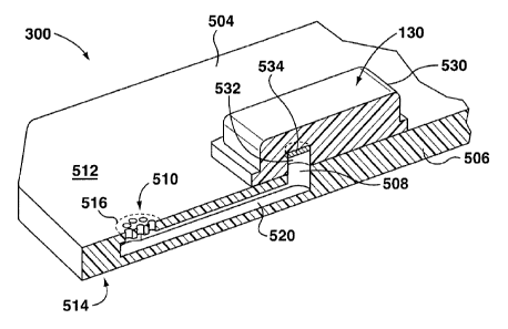
[0036] Referring now to Figures 5 to 8, one example embodiment of a
microphone assembly 500 for the portable electronic device 100 in accordance
with
the present disclosure will be described. The microphone assembly 500
comprises
a rigid printed circuit board (PCB) 504 comprising a board body 506 having one
or
more signal traces (not shown) for receiving electric audio signals generated
by the
microphone 130 and transmitting the electric audio signals to the processor
102.
The PCB 504 also comprises one or more power traces and one or more ground
traces. Alternatively, the PCB 504 may be a flexible PCB supported by a
stiffener
(not shown). The board body 506 has a top surface 512 and a bottom surface 514
located opposite to the top surface 512.
[0037] The PCB 504 typically comprises a number of signal traces, power
traces and ground traces separated by a non-conductive (i.e., dielectric)
material
such as a dielectric polymer. The PCB 504 typically comprises a number of
traces
each formed by a thin conductive foil patterned onto a dielectric substrate
(e.g.,
sheet). Each trace is patterned onto the dielectric substrate in a desired
circuit
pattern using, for example, conventional photolithography (or masking) and
etching
techniques. The conductive foil is typically copper, although conductive
materials
may be used. The PCB 504 forms a PCB stackup configuration which typically
comprises alternating core layers and prepreg layers which are laminated
together.
Core layers are thin layers of dielectric substrate having a trace patterned
on one or
more both sides. The dielectric substrate in the core layers is typically a
cured
fiberglass-epoxy resin. The prepreg layers are thin layers of the dielectric
substrate
which do not have any traces. The dielectric substrate in the prepreg layers
is
typically an uncured fiberglass-epoxy resin.
-9-
CA 02823965 2013-07-05
WO 2012/094722 PCT/CA2011/050012
[0038] The PCB 504 defines an acoustic channel 520 within the board body
506 which extends between a microphone aperture 508 in the board body 506 and
a plurality of inlet openings 510 in the board body 506. The inlet openings
510 are
typically arranged in a predetermined formation with the inlet openings 510
equally
spaced apart from each other for more uniform acoustic performance. The inlet
openings 510 are relatively small in size, e.g., 40 to 80 pm in diameter in
some
embodiments.
[0039] In one embodiment, the acoustic channel 520 is formed in the PCB
504 during the lamination process of its manufacture. To form the acoustic
channel
520, some of the core and prepreg layers of the PCB stackup are formed with
holes
in the dielectric substrate. The core and prepreg layers are aligned during
the
lamination process so that holes in adjacent layers are aligned, the holes in
adjacent layers collectively forming the acoustic channel 520. In some
embodiments, the acoustic channel 520 may have a depth (or height) of
approximately 440 pm. After the core and prepreg layers have been laminated
together, the microphone aperture 508 is mechanical drilled using depth
controlled
drilling techniques. The plurality of inlet openings 510 are then formed using
laser
drilling. Any excised PCB material in the acoustic channel 520 following
drilling
operations is removed. The plurality of inlet openings 510 are laser drilled
with a
diameter of 40 pm, 80 pm or other suitable diameter.
[0040] In other embodiments, the microphone aperture 508 and plurality of
inlet openings 510 may be formed using laser drilling, or may be formed using
a
series of holes in adjacent layers similar to the manner in which the acoustic
channel 520 is formed.
[0041] The microphone aperture 508 and the plurality of inlet openings 510
may be defined on a common surface of the board body 506, or on different
surfaces of the board body 506. In the shown example, the plurality of inlet
openings 510 are defined in the top surface 512 of the board body 506 along
with
the microphone aperture 508 and microphone 130 (Figure 1). In other
embodiments, the plurality of inlet openings 510 may be defined in the bottom
-10-
CA 02823965 2013-07-05
WO 2012/094722 PCT/CA2011/050012
surface 514 of the board body 506 while the microphone aperture 508 and
microphone 130 are located on the top surface 512 opposite to the plurality of
inlet
openings 510.
[0042] The microphone assembly 500 also comprises a microphone 130 which
is mounted to the board body 506. The microphone 130 is electrically connected
to
the signal trace in the board body 506. Electrical contacts (not shown) of the
microphone 130 are electrically connected to corresponding electrical contacts
on
the PCB 204. The microphone 130 comprises a casing 530 which defines an
opening 532. The operational components of the microphone 130, including an
acoustic-to-electric transducer 534 for converting acoustic audio signals into
electrical audio signals, are located inside in the casing 530. The transducer
534 is
located inside the casing 530 proximate to the opening 532 in the casing and
the
microphone aperture 508 in the board body 506.
[0043] The microphone 130 is radio frequency (RF) shielded to isolate the
microphone 130 from electromagnetic interference. Electromagnetic interference
may originate from signals received and generated by antennas (not shown)
which
are part of the communication subsystem 104. In other embodiments, a non-RF
shielded microphone could be used in which case an RF shield (not shown) may
be
provided to cover the microphone 130 on the PCB 504 to provide an
electromagnetic shield to assist in isolating the microphone 130 from
electromagnetic interference. RF shield cans are known in the art and so will
not be
described herein.
[0044] As best shown in Figure 7, the plurality of inlet openings 510 is
located
below the microphone inlet 204 in the front face 202 of the housing 200. The
plurality of inlet openings 510 in the board body 506 is in approximate
alignment
with the microphone inlet 204 in the housing 200, thereby allowing acoustic
audio
signals from an environment outside of the portable electronic device 100 to
pass
into and through the acoustic channel 520 and reach the microphone 130. In the
shown example, an air gap within the housing 200 separates the front face 202
from the PCB 504. The air gap is sealed to create a sealed acoustic path
between
-11-
CA 02823965 2013-07-05
WO 2012/094722 PCT/CA2011/050012
the microphone 130 and the environment outside of the portable electronic
device
100 as described below. In other embodiments, the inner surface of the front
face
202 may meet the top surface 512 of the PCB 504 such that there is
substantially
no air gap separating the front face 202 from the PCB 504.
[0045] The operation of the acoustic channel 520 will now be briefly
described. Acoustic audio signals from the environment outside of the portable
electronic device 100 pass through the microphone inlet 204 in the front face
202
and into the plurality of inlet openings 510. The acoustic audio signals then
pass
from the plurality of inlet openings 510 through the acoustic channel 520 to
the
microphone aperture 508 in the board body 506. The acoustic audio signals then
pass from the microphone aperture 508 in the board body 506 through the
opening
532 in the casing 530 of the microphone 130. The acoustic audio signals are
then
picked up by the acoustic-to-electric transducer 534 which converts the
acoustic
audio signals into electrical audio signals which are transmitted to the
processor
102 via the PCB 504.
[0046] The acoustic channel 520 in its shape and geometry provides an
acoustic waveguide or a resonator due to acoustic wave propagation inside the
acoustic channel 520. The acoustic wave propagation causes standing waves at a
first resonance at higher frequencies of the acoustic frequency band,
typically
greater than 4 kHz to 5 kHz for narrowband telephony. The length of the
acoustic
channel 520 determines the frequency of the first resonance. The frequency of
the
acoustic channel 520 is typically selected so that the first resonance is
close to, or
within, the band limits of transmitted speech/audio (typically in the range of
4 kHz
to 10 kHz) resulting in unwanted resonance effects. To control the resonance
effects of the acoustic channel 520 to avoid negative effects on speech
quality,
acoustic resistive elements are typically used at the end of the acoustic
channel 520
close to the microphone inlet 204 in the housing 200 or directly at the
microphone
inlet 204.
[0047] In the shown example, the plurality of small inlet openings 510 in
the
board body 506 having a high acoustic resistance are used as acoustic
resistive
-12-
CA 02823965 2013-07-05
WO 2012/094722 PCT/CA2011/050012
elements. The plurality of inlet openings 510 avoid the need for a mesh screen
which provides resonance dampening for the acoustic waveguide shaped by the
acoustic channel 520 in front of the microphone 130 and protects against
foreign
objects entering the interior of the housing 200 and the acoustic channel 520.
The
plurality of inlet openings 510 in the board body 506 are grouped within a
microphone inlet area 516 of the board body 506. The microphone inlet area 516
is
approximately the same size and shape as the microphone inlet 204 in the
housing
200. The inlet openings 510 in the shown example are generally circular.
Circular-
shaped inlet openings 510 may be easier to manufacture than other shapes and
may have better acoustic performance. Inlet openings 510 of different shapes
may
be used in other embodiments.
[0048] Numerous permutations of the size and number of inlet openings 510
are possible. The plurality of inlet openings 510 define an open area in the
top
surface 512 of the PCB 504 of between approximately 0.2 mm2 and approximately
0.4 mm2, which is thought to provide suitable acoustic performance. In some
example embodiments, the plurality of inlet openings 510 are each
approximately
80 pm in diameter and number between 10 and 20, which may be used to provide
the open area of between approximately 0.2 mm2 and approximately 0.4 mm2. In
other example embodiments, the plurality of inlet openings 510 are each
approximately 40 pm in diameter and number between 40 and 80 and are used to
provide the open area of between approximately 0.2 mm2 and approximately 0.4
mm2. Openings of approximately 40 pm in diameter approximate the size of the
openings of acoustic mesh screens, which have well known acoustic performance.
However, openings of approximately 40 pm in diameter are more difficult to
achieve using manufacturing techniques though such sizes will become more
readily
attainable as manufacturing techniques continue to improve. A different size
and
number of inlet openings 510 may be used in other embodiments.
[0049] The size and shape of microphone inlet 204 in the front face 202
of the
housing 200 is designed to meet acoustic requirements. In particular, the size
should be sufficiently large to allow acoustic audio signals from the
environment
(e.g., a user's voice during a voice call) to pass into the interior of the
housing 200
-13-
CA 02823965 2013-07-05
WO 2012/094722 PCT/CA2011/050012
and reach the plurality of inlet openings 510. However, the size should be
sufficiently small to still provide effective protection against foreign
objects (e.g.,
dust) entering the interior of the housing 200 and the acoustic channel 520,
to
minimize its effect on the appearance of the front face 202 of the housing
200, or
both. Similarly, the size and shape of the plurality of inlet openings 510,
the
microphone aperture 508 in the board body 506, and the opening 532 in the
microphone casing 530 are designed to meet acoustic requirements, in
particular,
the size and shape should allow acoustic audio signals to enter the acoustic
channel
520 and pass through to the transducer 534 of the microphone 130.
[0050] As best shown in Figures 7 and 8, a sealing member 540, such as a
rubber gasket, may be provided in some embodiments. The sealing member 540 is
used to reduce or avoid acoustic couping between the speaker 128 and the
microphone 130 within the portable electronic device 100 to avoid echo. The
sealing member 540 seals the PCB 504 to the inner surface of the front face
202 of
the housing 200. The sealing member 540 may be made of a compressible, non-
conductive material such as rubber. The microphone inlet area 516 is
configured to
fit within an inside dimension of the sealing member 540 which surrounds the
microphone inlet area 516 of the board body 506 and seals the board body 506
against the inner surface of the housing 200.
[0051] In the shown example embodiment, the plurality of inlet openings
510
in the board body 506 are arranged in a generally circular formation and the
sealing
member 540 is a circular rubber gasket which surrounds the microphone inlet
area
516, which is correspondingly generally circular in shape. In other
embodiments,
the plurality of inlet openings 510 in the board body 506 may be arranged in a
different shape, such as generally square or rectangular formation, resulting
in a
correspondingly shaped microphone inlet area 516, such as a generally square
or
rectangular shape. The shape of the sealing member 540 is typically selected
to
correspond to that of the microphone inlet area 516 to provide a generally
uniform
clearance resulting in a generally square or rectangular rubber gasket in such
embodiments. A generally square or rectangular formation of inlet openings 510
-14-
CA 02823965 2013-07-05
WO 2012/094722 PCT/CA2011/050012
may be easier to manufacture. The clearance may be approximately 0.1 mm in
some embodiments.
[0052] In some example embodiments, the plurality of inlet openings 510
in
the board body 506 are arranged in a generally circular formation and the
sealing
member 540 is a circular rubber gasket having a thickness of approximately 0.2
to
0.3 mm and an inside diameter of approximately 1 mm. A clearance of
approximately 0.2 to 0.3 mm may be provided between an inside dimension of the
sealing member 540 and the periphery of the microphone inlet area 516,
resulting
in a microphone inlet area 516 having a generally circular area approximately
0.4
to 0.6 mm in diameter. The dimensions described immediately above are examples
provided for illustration and are not intended to be limiting. Other
dimensions are
possible. The dimensions described immediately above are dependent, at least
in
part, on the mechanical tolerances of the parts which may be 0.1 mm in some
example embodiments.
[0053] In other embodiments, for example when the speaker 128 is not part
of the acoustic environment (e.g., as is typical for flip phones and other
flip-style
portable electronic devices), the area around the microphone inlet area 516 of
the
PCB 504 may be sealed directly against the inner surface of the front face 202
of
the housing 200 without a sealing member 540.
[0054] Referring now to Figures 3 and 4, another example embodiment of a
microphone assembly 300 for the portable electronic device 100 in accordance
with
the present disclosure will be described. The microphone assembly 300
comprises
a PCB 504 generally similar to that of the microphone assembly 500 described
above. However, instead of a plurality of inlet openings 510 defined in the
PCB 504
at the end of the acoustic channel 520 opposite to the microphone aperture 508
in
the board body 506, a larger, single aperture 550 is defined. In the shown
example, the aperture 550 is located on the top surface 512 of the board body
506
with the microphone aperture 508. However, the aperture 550 may be located on
the bottom surface 514 of the board body 506 opposite to the microphone
aperture
508 and microphone 130.
-15-
CA 02823965 2013-07-05
WO 2012/094722 PCT/CA2011/050012
[0055] A mesh screen (not shown) is provided between a sealing member
(not shown) and the front face 202 of the housing 200. The sealing member may
be the same or similar to the sealing member 540 described above in connection
with the microphone assembly 500. The mesh screen provides acoustic resonance
dampening for the acoustic waveguide shaped by the acoustic channel 520 in
front
of the microphone 130 and protects against foreign objects entering the
interior of
the housing 200 and the acoustic channel 520. The mesh screen may be made, for
example, from stainless steel or fabric cloth. The mesh screen is designed to
meet
acoustic requirements. The mesh screen may be secured against the inner
surface
of the front face 202 of the housing 200 using a suitable adhesive.
Alternatively,
the sealing member 540 may press the mesh screen against the inner surface of
the front face 202 of the housing 200 to hold it in place. Alternatively, the
mesh
screen may be provided within the sealing member 540.
[0056] Referring now to Figure 9, a further example embodiment of a
microphone assembly 900 for the portable electronic device 100 in accordance
with
the present disclosure will be described. The microphone assembly 900
comprises
a rigid PCB 504 generally similar to that of the microphone assembly 300 and
microphone assembly 500 described above with the notable exception that the
acoustic channel 560 has an open top rather than a closed top. The acoustic
channel 560 may be formed duration lamination of the PCB 504 as describe
above,
or may be drilled, milled or otherwise formed in a first surface of the PCB
504. In
the shown example, the acoustic channel 560 is formed in the top surface 512
of
the PCB 504. The acoustic channel 560 is formed in the dielectric substrate of
the
PCB 504 in a manner which does not interfere with its various traces.
[0057] The microphone assembly 900 also comprises a waveguide 562 which
extends substantially parallel to the first surface of the board body 506. The
waveguide 562 is formed from an acoustically reflective material, which may be
steel, plastic or the PCB material, and may be soldered or glued airtight
against the
PCB 504. The waveguide 562 is a lid or cover which partially covers an open
top of
the acoustic channel 560 and exposes a first portion of the acoustic channel
560.
The exposed first portion of the acoustic channel 560 defines an inlet opening
566.
-16-
CA 02823965 2013-07-05
WO 2012/094722 PCT/CA2011/050012
A microphone aperture 508 is defined by the PCB 504 on a second surface
located
directly across from the first surface in which the acoustic channel 560 is
defined.
In the shown example, the microphone aperture 508 is defined in the bottom
surface 514 of the PCB 504. The acoustic channel 560 and waveguide 562
collectively define the acoustic channel 560 in the covered portion extending
between the microphone aperture 508 and the inlet opening 566. The inlet
opening
566 in the board body 506 and the microphone inlet 204 in the housing 200 are
in
approximate alignment similar to the plurality of inlet openings 510 in the
board
body 506 of the microphone assembly 500 described above, and the aperture 550
in the board body 506 of the microphone assembly 300 described above.
[0058] Referring now to Figure 10, a further example embodiment of a
microphone assembly 1000 for the portable electronic device 100 in accordance
with the present disclosure will be described. The microphone assembly 1000
comprises a rigid PCB 504 generally similar to that of the microphone assembly
900
described above. However, the waveguide 562 exposes a further portion 568 of
the acoustic channel 560 which defines the microphone aperture 508 of the
acoustic channel 520. The exposed first portion 566 and the exposed further
portion 568 are located towards opposite ends of the acoustic channel 520 on
the
first surface (e.g., top surface 512 or bottom surface 514) of the PCB 504.
[0059] The microphone assembly 900 and microphone assembly 1000 may
allow for a PCB with a reduced thickness compared to the other embodiments
described herein since additional layers of the PCB 504 above the acoustic
channel
may be replaced with a lid or cover which partially covers the open top of the
acoustic channel to form a waveguide 562. A lid may be used when the
additional
layers of the PCB 504 are not required to provide circuitry for other device
components. The lid may be quite thin to reduce thickness of the PCB as much
as
possible.
[0060] Referring now to Figure 11, a further example embodiment of a
microphone assembly 1100 for the portable electronic device 100 in accordance
with the present disclosure will be described. The microphone assembly 1100
-17-
CA 02823965 2013-07-05
WO 2012/094722 PCT/CA2011/050012
comprises a rigid PCB 504 generally similar to that of the microphone assembly
300
and microphone assembly 500 described above. However, the microphone 130 is
received in the acoustic channel 520. Although a plurality of inlet openings
510
which are acoustically connected to the acoustic channel 520 are defined in
the
board body 506 in the shown example, a large single inlet opening in the board
body 506 may be used instead of the plurality of inlet openings 510 in other
embodiments. The single inlet opening is similar to the aperture 550 of the
microphone assembly 300 described above.
[0061] The microphone 130 is a MicroElectrical-Mechanical System (MEMS)
microphone 570, also referred to as a microphone chip, silicon microphone or
reflow microphone. The MEMS microphone 570 comprises a pressure-sensitive
diaphragm etched into a silicon chip using MEMS techniques. The pressure-
sensitive diaphragm may be provided with an integrated preamplifier and may
have
a built in analog-to-digital converter (ADC) circuit so as to provide a
digital
microphone. Alternatively, the MEMS microphone may be connected to an
application-specific integrated circuit (ASIC). The MEMS microphone 570 may be
electrically connected to the signal trace of the PCB 504 within the acoustic
channel
520 via a conductive adhesive, thereby avoiding the need to solder or
otherwise
surface mount the microphone 130 to the PCB 504 and eliminating any sealing
issues resulting from surface mounting the microphone 130. The MEMS microphone
570 may also be electrically connected to a ground trace of the PCB 504 so as
to
ground the MEMS microphone 570. The microphone assembly 1100 reduces the
amount of surface area of the PCB 504 which is required for acoustic
integration of
the microphone 130, and provides electrostatic discharge (ESD) protection of
the
microphone 130 when the MEMS microphone 570 is grounded to a ground trace of
the PCB 504. The microphone assembly 1100 reduces acoustic leakage when using
acoustic porting in the PCB 504 since the MEMS microphone 570 is already
embedded into the PCB 504. Embedding the MEMS microphone 570 in the PCB 504
removes one port and one potential source of acoustic leakage.
[0062] In other embodiments, when the layers of the PCB 504 are not
required to provide circuitry for other device components, the layers of the
PCB 504
-18-
CA 02823965 2013-07-05
WO 2012/094722 PCT/CA2011/050012
above the acoustic channel may be replaced with a lid or cover which partially
covers an open top of the acoustic channel to form a waveguide as described
above
in connection with the microphone assembly 900 and microphone assembly 1000.
The may be used to reduce the thickness of the PCB 504 as described above.
[0063] The microphone assembly described in the present disclosure allows
the microphone 130 to be located away from the microphone inlet 204 in the
housing 200 of the portable electronic device 100 without requiring a
microphone
tube (also known as a microphone boot) and its associated drawbacks.
[0064] A microphone tube is conventionally used to provide an acoustic
channel or path between a microphone 130 and a microphone inlet 204. A
microphone tube is a complex mechanical part, typically formed from rubber,
which
seals against the microphone as well as the microphone opening. Microphone
tubes
occupy a relatively large amount of space on the PCB and thereby impose
restrictions on the location of other device components.
[0065] A microphone 130 may be located away from the microphone inlet 204
for several reasons, typically because another device component is mounted to
the
PCB 504 in the area proximate to the microphone inlet 204, or because the area
proximate to the microphone inlet 204 is restricted. For example, antennas
(not
shown) which are part of the communication subsystem 104 are sometimes
mounted to the PCB 504 in the area proximate to the microphone inlet 204. In
such cases, the microphone 130 should not be located in the area around the
antenna to reduce or eliminate RF electromagnetic interference with the
microphone 130. The microphone assembly described herein provides an
alternative to a microphone tube which allows the microphone 130 to be located
away from the microphone inlet 204, thereby freeing up space on PCB 504 for
other
device components or a reduction in the footprint/size of the PCB 504,
depending
on design constraints.
[0066] In the above described examples, an acoustic channel formed in the
PCB 504 is used for acoustic porting of sound from an environment outside of
the
portable electronic device 100 to a microphone inside of the portable
electronic
-19-
CA 02823965 2015-04-02
device 100. An acoustic channel may also be used as air tube or air cavity for
porting sound from the speaker 128 through the PCB 504 to the environment
outside of the portable electronic device 100.
[0067] The described embodiments are to be considered in all respects
as
being only illustrative and not restrictive. The present disclosure intends to
cover
and embrace all suitable changes in technology. The scope of the present
disclosure is, therefore, described by the appended claims rather than by the
foregoing description. All changes that come within the meaning and range of
equivalency of the claims are intended to be embraced within their scope.
-20-