Note: Descriptions are shown in the official language in which they were submitted.
CA 02824128 2013-07-08
WO 2012/095673 PCT/GB2012/050071
1
DUAL ANTENNA STRUCTURE HAVING CIRCULAR POLARISATION
CHARACTERISTICS
[0001] Embodiments of the present invention relate to an antenna structure
comprising
an active arm and a passive arm, the arms being disposed in such a way as to
create a
circularly polarised radiation pattern that is good for personal navigation
devices (PNDs),
automotive Global Positioning System (GPS) receiver applications, GPS-enabled
cameras
and the like. In particular, but not exclusively, embodiments of the present
invention
provide a substantially thinner GPS radio antenna solution than conventional
ceramic
patch antennas, when used in the above devices, thereby enabling thinner
consumer
products to be designed.
BACKGROUND
[0002] Many existing navigation and other GPS-enabled devices use a ceramic
patch
antenna connected to a GPS receiver. This is because ceramic patch antennas
offer
several advantages. Firstly, provided that the ceramic patch is not too small,
good right-
hand circular polarization (RHCP) can be obtained. GPS radio signals are
transmitted
using RHCP. Generally, ceramic patch antennas larger than about 15mm x 15mm x
4mm
provide good RHCP reception. Also, the radiation pattern of a horizontally
mounted
ceramic patch antenna gives good coverage of the upper hemisphere when the
patch is
mounted horizontally at the top of a device and facing the sky. Circular
polarization is also
used in many other telecommunication systems, such as SDARS and DVB-SH.
[0003] Unfortunately, ceramic patch antennas also suffer from significant
drawbacks.
When the patch is made smaller and more commensurate with the requirements of
modern consumer devices (patch sizes typically 12mm x 12mm x 4mm or less) most
of the
advantages are lost. The RHCP characteristic is reduced and the polarization
becomes
more linear unless a large ground plane is placed under the antenna, which is
not practical
in a mobile or hand-held device. Also the efficiency is reduced and the
radiation pattern
becomes more omnidirectional, with less gain toward the sky. Furthermore, the
bandwidth
of the antenna becomes very narrow, making manufacturing tolerances critical
and
increasing the cost.
[0004] In general, ceramic patch antennas have a very high Q and cannot be
fine-tuned
using external matching circuits. The high Q implies a narrow bandwidth and
this in turn
means that in different applications the same antenna requires tuning in order
to be on
frequency. Because matching circuits cannot be used, the ceramic patch has to
be
physically changed to tune it for a specific design. This requirement for
physically
CA 02824128 2013-07-08
WO 2012/095673 PCT/GB2012/050071
2
changing the antenna increases the cost and the length of the integration
process for
every new application. Essentially, a new ceramic patch design must be created
for each
application.
[0005] Perhaps the greatest disadvantage of the ceramic patch antenna is the
severe
constraint it places upon the minimum thickness of a GPS-enabled device, as
the
thickness must be at least 12mm to accommodate the ceramic patch. In a typical
application, such as a navigation device in a car, there is a vertically
mounted flat-screen
display and potentially the device could be made quite thin were it not for
the need to
encompass the width of the ceramic patch. Finally, ceramic patches are
expensive to
manufacture compared to many other types of small antenna.
[0006] Figure la shows a typical GPS-enabled consumer device comprising an LCD
display 1, a main PCB 2, a groundplane 3 and a ceramic patch antenna 4. Figure
lb
shows how the minimum device thickness is dictated by the antenna 4, which is
mounted
horizontally on top of the vertical PCB 2.
[0007] Although other types of antenna are available that can solve some the
above
issues, none really match the performance of a large patch for GPS
applications and so
where optimal performance is required, large patches continue to be used and
consumer
devices are made thick enough to encompass the patch.
[0008] An example of a known antenna is disclosed in US2008/0158088, in the
form of a
class of thin antenna for GPS applications. However, such antennas are
linearly polarized
(see paragraph [0009]), and therefore not comparable with modern ceramic patch
antennas. A further drawback of the antennas disclosed in US2008/0158088 is
that in
order to feed the antenna it is necessary to solder a coaxial cable directly
to the antenna
structure, and the antenna cannot be fed directly by the host PCB. This also
means that
there is no provision for a matching circuit, so the antenna must be self-
resonant at the
desired frequency, and the physical structure of the antenna must be changed
in order to
adjust the antenna to any particular host device.
[0009] Another example of a known antenna is disclosed in US2007/0171130.
Although
the superficially similar to some embodiments of the present invention, there
are important
differences. First of all the problem to be solved is very different, as
US2007/0171130
teaches how to design an elongated multi-band antenna with broadband function
for
cellular communications, and no importance is given to the circular
polarization properties
of the waves generated by the antenna and the shape of the radiation pattern,
which are
important for satellite communications.
Furthermore, the structure defined in
US2007/0171130 requires a connection using coaxial cable soldered directly to
the
CA 02824128 2013-07-08
WO 2012/095673 PCT/GB2012/050071
3
antenna, and therefore it suffers from the same drawbacks discussed above for
US2008/0158088.
[0010] A further antenna is known from EP0942488A2. In this case the antenna
can
generate a circular polarized wave; however, because the two arms forming the
antenna
are arranged in perpendicular directions, such type of antenna is not suitable
for
application in thin devices. The same consideration applies to the antenna
type disclosed
in US2008/0284661.
[0011] US20055/0057401 discloses an antenna comprising an active arm and a
passive
arm that are mounted over a groundplane with a slot between the two arms.
However, the
groundplane is much larger in area than the area under the active and passive
arms, and
the arms are all fed and grounded at the same end of the antenna device. This
antenna is
not stated to have any circular polarization properties, nor can it be formed
from a single
sheet of metal.
[0012] The problem to be solved is thus to create a low-cost antenna that
occupies a
small space, can fit inside thin flat-screen devices, requires little or no
customisation when
installed on many different types of platform and yet will give the
performance of a ceramic
patch antenna.
BRIEF SUMMARY OF THE DISCLOSURE
[0013] According to a first aspect of the present invention, there is provided
an antenna
device comprising at least first, second and third conductive metal plates
arranged in a
substantially parallelepiped configuration, with the third plate defining a
lower plane and
the first and second plates together defining an upper plane substantially
parallel to the
lower plane, wherein: the first and second plates are substantially similar in
shape and are
of substantially the same length as each other along a major axis of the
antenna; the first
and second plates are separated by a slot in the upper plane, the slot
extending along the
major axis of the antenna and having a length similar to the length of each of
the first and
second plates; the first plate comprises an active antenna arm that is
provided with a feed
connection; the second plate comprises either a passive antenna arm that is
provided with
a grounding connection to the third plate, or a second active antenna arm that
is provided
with a grounding connection to the third plate and also with a feed
connection; and wherein
the feed or grounding connections are not all formed on a single side of the
parallelepiped
arrangement of plates.
CA 02824128 2013-07-08
WO 2012/095673 PCT/GB2012/050071
4
[0014] The feed connection of the active antenna arm preferably extends
substantially
perpendicular to the third plate and passes through a slot or hole provided in
the third
plate.
[0015] The feed connection may be formed as an integral feed pin which extends
through and beyond the third plate. This is an important feature of certain
embodiments,
as it allows the direct connection of the antenna to a host device without the
use of
expensive coaxial cables. Moreover, in this way the antenna can be connected
to a
matching circuit, which can be used to adjust the resonant frequency of the
antenna
without the need of modifying the physical structure of the antenna. This
feature makes it
possible to use of the same antenna on many different devices without
expensive
customization.
[0016] In order to achieve circular polarization behaviour, the length of the
slot in the
upper plane between the first and second plates must be similar to the length
of the first
and second plates themselves, although the exact shape of the slot is not
currently
believed to be a critical feature for some embodiments. The special feature
that the feed
or grounding connections are not all formed on a single side of the
parallelepiped
arrangement of plates helps to promote circular polarization.
[0017] In preferred embodiments, the first, second and third plates are made
from a flat
sheet of metal by cutting and bending. In particular, the third plate and at
least one or
other, and in some cases both, of the first and second plates, may be formed
from a single
sheet of metal that is appropriately cut and then bent into shape. The feed
connection
may be made from the same metal sheet.
[0018] Embodiments of the present invention are to be distinguished from
antennas that
are formed by way of printed conductive tracks. In particular, the plates of
embodiments of
the antennas of the present invention may comprise relatively stiff metal
structures which
retain their own shape without the need for an underlying substrate.
[0019] In alternative embodiments, antenna devices of the present invention
may be
manufactured using a flexible printed circuit wrapped around a non-conductive
mechanical
support, or by using a Laser Direct Structuring (LDS) process, where the shape
of the
conductive part of the antenna device is imprinted on a plastic or dielectric
support using a
laser, followed by plating the support in such a way that only the parts of
the support that
have been activated by the laser are metallized. Alternatively, the plates may
be formed
by etching a metal layer formed on or bound to a non-conductive support.
[0020] Preferred embodiments have a rectangular parallelepiped shape with
typical
dimensions 25mm x 5mm x 4mm or less for the GPS frequency band, allowing a
CA 02824128 2013-07-08
WO 2012/095673 PCT/GB2012/050071
significant reduction of the total thickness of a consumer device from around
12 mm to 5
mm or less.
[0021] The antenna works optimally in the same position as a ceramic patch at
the top of
a device, facing the sky. The antenna can be fine tuned to the correct
frequency using a
5 simple external matching circuit, allowing the same antenna to be used in
many different
designs without mechanical changes.
[0022] Importantly, for GPS applications, the antenna is almost purely
circularly polarized
(RHCP or LHCP) when used in isolation (not connected to a big ground plane).
Circular
polarization is created by the combination of the electromagnetic field
radiated by the slot
between the first and second plates, and the electromagnetic field radiated by
the radio-
frequency current circulating around the loop-like path formed by the three
plates together.
Furthermore, the circular polarisation characteristic is maintained to a good
degree when
the antenna is connected to a large ground plane, for instance at the top of
different
application device PCBs or on top of LCD displays. When located in this way,
similar to
the way a ceramic patch antenna is disposed, the antenna generates a
hemispherical
radiation pattern similar to that of a patch antenna, which is suitable for
some applications
such the reception of GPS signals.
[0023] The antenna has significant cost advantages over ceramic patches
because it
may be manufactured from a single metal sheet, thereby considerably reducing
the
manufacturing cost.
[0024] In a first embodiment of the present invention, an antenna is
constructed from a
single flat piece of metal by cutting and bending. The lower plate is grounded
and two
upper plates or arms are provided with grounding connections to the lower
plate, the
grounding connections being at opposed ends of the lower plate. One upper arm
is active
and driven by a feeding pin, located in between the opposed ends of the
antenna device,
in a manner reminiscent of the way a planar inverted F antenna is fed with the
grounding
connection at one end. The other arm is passive and has only the ground
connection.
[0025] In a second embodiment of the present invention, an antenna is
constructed from
a single flat piece of metal by cutting and bending. A lower plate is grounded
and two
upper plates or arms are provided with grounding connections to the lower
plate. One
upper arm is active and driven by a feeding pin at one end and grounded by a
grounding
connection to the lower plate along a long edge of the lower plate in between
the two ends
of the lower plate. The feeding and grounding arrangements are reversed with
respect to
the first embodiment. The other arm is passive and has only the ground
connection at an
end of the lower plate opposed to the end where the feeding pin of the active
upper arm is
located.
CA 02824128 2013-07-08
WO 2012/095673 PCT/GB2012/050071
6
[0026] In a third embodiment of the present invention, an antenna is
constructed from
two separate flat pieces of metal by cutting and bending. The active arm is
driven by a
feeding pin at one end and no provision is made for grounding. A separate
lower plate is
grounded and supports a second, passive arm that has a grounding connection to
the
lower plate at an end opposed to the end where the feeding pin of the active
arm is
located. Because the antenna is manufactured from two separate metal pieces
the
structure is not wholly self-supporting and there is need of a non-conducting
or dielectric
mechanical supporting mechanism. This support may take the form of a block of
non-
conducting or dielectric mechanical, or pillars or even a plastic 'carrier'
that clips, or is
screwed, to the PCB and which holds one or more of the metal arms in place.
Various
other mechanical arrangements may be made to support the two arms.
[0027] In a fourth embodiment, both arms are fed and both are grounded. The
second
arm is fed with a signal out of phase with respect to the first arm as a form
a differential
feeding. The concept of having two PIFAs with a slot between them and feeding
both with
a phase difference is already known from Kan et al. [H.K. Kan, D. Pavlickovski
and R.B.
Waterhouse, "Small dual L-shaped printed antenna", ELECTRONICS LETTERS, Vol.
39,
No. 23, 13th November 2003]. However, Kan et al. describe a printed PIFA and
they do
not teach having a lower grounded plate to connect the two structures
together. It will be
appreciated that the differential feeding of both arms may be applied to the
first three
embodiments and also to the additional case where one arm is grounded and the
other is
not. It will also be appreciated that in all these embodiments, one feed may
be connected
to the radio and the other grounded as an alternative to differential feeding.
[0028] Moreover, with two feeding points, it is also possible to generate RHCP
when
using one feed and to generate LHCP when using the other feed.
[0029] It will also be appreciated that both, or either, arms may be provided
with a
matching circuit in all the embodiments above.
[0030] In the embodiments outlined above, the antenna has been described as a
stand-
alone component separate from the radio. However, the presence of the bottom
ground
plate allows the possibility of attaching a small PCB mounted with the
components
required for a RF front end (Low Noise Amplifier plus a Surface Acoustic Wave
filter) or a
complete radio receiver. In this way, an active antenna or complete radio-
antenna module
is created. The input to the LNA or radio receiver may be connected to the
feed of the
antenna and the ground of the LNA or radio may be connected to the bottom
ground plate
of the antenna. The output of the radio/LNA may be connected to the host PCB
using a
commercially available connector, coaxial cable or via soldering pins.
CA 02824128 2017-01-09
51331-1453
7
[0031] In another embodiment, the stamping, cutting and bending
process
used to create the antenna from a sheet of metal may also be used to create a
screened volume beneath the ground or third plate suitable for locating the
radio.
The radio-antenna module is thus created with an integral screening can for
the
radio.
[0032] The third plate may be provided with one or more conductive
tabs to
facilitate connection of the antenna device to a host device. The one or more
conductive tabs may be disposed in a coplanar configuration with the feed
connection.
[0032a] According to another aspect of the present invention, there is
provided
an antenna assembly comprising: a first conductive plate and a second
conductive
plate both co-planar in a first plane; and a third conductive plate positioned
in a
second plane substantially parallel to the first plane, the three conductive
plates being
assembled to form a parallelepiped antenna configuration that transmits or
receives
circularly polarized signals, the parallelepiped antenna configuration having
a first
side in the first plane, a second side in the second plane and four inter-
plane sides
intersecting the first and second sides, each of the first conductive plate
and the
second conductive plate having one or more conductive connections to the third
conductive plate, at least one of the conductive connections of each of the
first
conductive plate and the second conductive plate being formed along a
different one
of the four inter-plane sides of the parallelepiped antenna configuration,
each of the
four inter-plane sides having no more than one conductive connection formed
along
the same inter-plane side.
[0032b] According to still another aspect of the present invention,
there is
provided a method comprising: forming an antenna assembly including a first
conductive plate and a second conductive plate both co-planar in a first plane
and a
third conductive plate positioned in a second plane substantially parallel to
the first
plane, the three conductive plates being assembled to form a parallelepiped
antenna
CA 02824128 2017-01-09
51331-1453
7a
configuration that transmits or receives circularly polarized signals, the
parallelepiped
antenna configuration having a first side in the first plane, a second side in
the
second plane and four inter-plane sides intersecting the first and second
sides, each
of the first conductive plate and the second conductive plate having one or
more
conductive connections to the third conductive plate, at least one of the
conductive
connections of each of the first conductive plate and the second conductive
plate
being formed along a different one of the four inter-plane sides of the
parallelepiped
antenna configuration, each of the four inter-plane sides having no more than
one
conductive connection formed along the same inter-plane side.
[0032c] According to yet another aspect of the present invention, there is
provided a method comprising: generating radiation having circular
polarization from
an antenna assembly having a first conductive plate and a second conductive
plate
both positioned co-planar in a first plane and a third conductive plate
positioned in a
second plane substantially parallel to the first plane, the three conductive
plates being
assembled to form a parallelepiped antenna configuration that transmits or
receives
circularly polarized signals, the parallelepiped antenna configuration having
a first
side in the first plane, a second side in the second plane and four inter-
plane sides
intersecting the first and second sides, each of the first conductive plate
and the
second conductive plate having one or more conductive connections to the third
conductive plate, at least one of the conductive connections of the first
conductive
plate and the second conductive plate being formed along a different one of
the four
inter-plane sides of the parallelepiped antenna configuration, each of the
four inter-
plane sides having no more than one conductive connection formed along the
same
inter-plane side.
[0032d] According to a further aspect of the present invention, there is
provided
an antenna assembly comprising: a first conductive plate and a second
conductive
plate both co-planar in a first plane; a third conductive plate positioned in
a second
plane substantially parallel to the first plane; and means for generating
circular
CA 02824128 2017-01-09
51331-1453
7b
polarization radiation from at least the first conductive plate and the second
conductive plate, the means including one or more conductive connections
between
the first plane and the second plane.
BRIEF DESCRIPTION OF THE DRAWINGS
[0033] For a better understanding of the present invention and to show how
it
may be carried into effect, reference shall now be made by way of example to
the
accompanying drawings, in which:
FIGURES la and lb show a prior art ceramic patch enabled GPS
receiving device;
FIGURE 2 shows a first embodiment of the present invention;
FIGURE 3 shows a second embodiment of the present invention;
FIGURE 4 shows a third embodiment of the present invention;
FIGURE 5 shows a fourth embodiment of the present invention;
FIGURES 6a and 6b show the radiation patterns of an antenna of the
present invention when used without connection to a groundplane;
FIGURES 7a, 7b and 7c show an embodiment of the present invention
connected to the PCB of a consumer navigation device;
FIGURES 8a and 8b show the radiation patterns of the antenna of
Figures 7a to 7c when connected to the groundplane of the consumer navigation
device; and
FIGURE 9 shows the impedance of an antenna of the present invention
across a frequency band of interest both before and after matching;
CA 02824128 2017-01-09
51331-1453
7c
FIGURE 10 shows a variation of the embodiment of Figure 2 configured
to generate LHCP;
FIGURES 11 and 12 show an embodiment comprising an antenna with
an integrated radio circuit;
CA 02824128 2013-07-08
WO 2012/095673 PCT/GB2012/050071
8
FIGURES 13 and 14 show an embodiment comprising an antenna with an
integrated radio circuit and a screening can made from an extension of the
ground plate;
and
FIGURE 15 shows an alternative mounting arrangement on a PCB substrate.
DETAILED DESCRIPTION
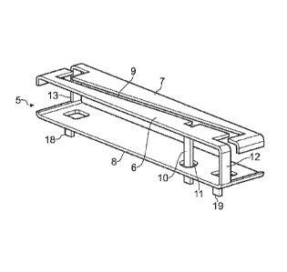
[0034] Figure 2 shows a first embodiment of the present invention, comprising
an
antenna device 5 consisting of first 6, second 7 and third 8 conductive metal
plates
arranged in a substantially parallelepiped configuration. The third plate 8
defines a lower
plane and the first 6 and second 7 plates together define an upper plane
substantially
parallel to the lower plane. The first 6 and second 7 plates are separated by
a slot 9 in the
upper plane.
[0035] The first plate 6 comprises an active antenna arm that is provided with
a feed
connection or pin 10 that passes through a hole 11 provided in the third plate
8. The first
plate 6 also has a grounding connection or pin 12 that connects to the third
plate 8.
[0036] The second plate 7 comprises a passive antenna arm that is provided
with a
ground connection or pin 13 that connects to the third plate 8 at an opposite
end thereof to
the ground connection or pin 12 of the first plate 6.
[0037] It can be seen that the overall envelope of the antenna device 5 is
that of a
rectangular parallelepiped, with the area of the first and second plates 6, 7
and their
intermediate slot 9 being substantially the same in size and shape as the area
of the third
plate 8, and substantially parallel thereto.
[0038] Tabs 18, 19 are created in the third plate 8 so as to allow the antenna
device 5 to
be soldered along the edge of a host PCB (not shown). The tabs 18, 19 provide
both a
mechanical support and a ground connection. The tabs 18, 19 are preferably
disposed in
the same plane as the feed connection or pin 10 so that soldering can be done
on a single
side of the host device. Alternatively, tabs 18, 19 and the feed 10 can be
arranged so that
they are connected to different sides of the host PCB.
[0039] Figure 3 shows a second, alternative embodiment which is substantially
the same
as the first embodiment, except in that the feed connection or pin 10 and the
ground
connection or pin 12 of the first plate 6 are swapped around. The feed
connection or pin
10 extends through the third plate 8 by way of a slot or cut-out 100 formed in
the third plate
8.
CA 02824128 2013-07-08
WO 2012/095673 PCT/GB2012/050071
9
[0040] In a third embodiment, shown in Figure 4, the first plate 6 is not
provided with a
ground connection or pin, but instead has only a feed connection or pin 10. In
this
embodiment, the first plate 6 is not physically connected to the third plate
8, and comprises
a separate sheet of metal. In order to provide structural integrity, it is
necessary for a non-
conductive mechanical support 14 to be provided between the third plate 8 and
the first
plate 6.
[0041] In a fourth embodiment, shown in Figure 5, both arms (i.e. both the
first plate 6
and the second plate 7) are fed and grounded. This arrangement is similar to
the
arrangement of Figure 2, with the addition of a feed connection or pin 15 for
the second
plate 7 and an additional hole 11' in the third plate 8 through which the feed
connection or
pin 15 may be passed. In this embodiment, the second plate 7 is fed with a
signal that is
out of phase with a signal that is fed to the first plate 6 so as to form a
differential feeding
arrangement.
[0042] In one exemplary embodiment (Figure 2) the antenna 5 is used without
connection to a groundplane. The radiation patterns are shown in Figures 6a (z-
x plane of
the antenna pattern) and 6b (y-z plane of the antenna pattern) and they can be
seen to be
the same as those of a dipole, except that the patterns exhibit strong RHCP.
The RHCP
response is better than the LHCP response by a factor of 10 dB or more. This
is very
good for an electrically small device.
[0043] In another exemplary embodiment (Figure 2) the antenna 5 is connected
to the
PCB 2 of a consumer navigation device or other GPS-enabled device, as
illustrated in
Figures 7a, 7b and 7c. It can be seen in Figure 7b that the antenna 5 is
easily soldered or
reflowed onto the edge of the PCB 2. Figure 7c shows that the minimum device
thickness
is no longer dictated by the antenna 5, but rather by the PCB 2, an LCD screen
1,
electronic circuitry 16 and a power supply 17.
[0044] Despite the perturbing influence of the groundplane, the antenna 5
still exhibits a
preference for RHCP, as can be seen in Figures 8a (y-z plane of the antenna
pattern) and
8b (z-x plane of the antenna pattern). Furthermore, the antenna 5 shows
excellent upward
radiation characteristics, as required for most navigation applications. In
this respect the
radiation pattern of the present invention is similar to that of a ceramic
patch antenna, but
the present invention is much thinner in profile and cheaper to manufacture.
[0045] An important advantage of embodiments of the present invention is that
they have
a wider impedance bandwidth than the sharp resonance of a ceramic patch
antenna. This
wider bandwidth makes it much easier to use in different applications.
Furthermore, the
antenna 5 is easily matched to the 50 ohm impedance typical of many RF systems
using a
simple LC matching circuit having typically one or two components. In
different
CA 02824128 2013-07-08
WO 2012/095673 PCT/GB2012/050071
applications, the resonant frequency of the antenna 5 can therefore be
adjusted simply by
changing the matching circuit, at least within a reasonable frequency range.
This is
considered advantageous in the integration and manufacturing process, as the
same
antenna 5 can be easily re-used in many different devices without any physical
or
5 mechanical change. Only the matching circuit needs to be changed. An
example of
matching the antenna in a typical application is shown in Figure 9.
[0046] In the exemplary embodiments shown so far the antenna 5 has been used
for
GPS applications where RHCP response and an upward radiation pattern response
is
preferred. However, in other applications, LHCP may be preferred. RHCP and
LHCP are
10 easily swapped by symmetry operations. Figure 10 shows a variation of
the embodiment
of Figure 2, using the same labelling of parts, that is configured to generate
LHCP. Other
radiation patterns may be created by disposing the antenna 5 in different
locations on the
PCB 2.
[0047] In the exemplary embodiments shown so far the antenna has been
described as
a stand-alone component separate from the radio. However, as shown in Figures
11 and
12, the presence of the bottom ground plate 8 allows the possibility of
attaching a small
PCB 20 mounted with the components required for a RF front end (Low Noise
Amplifier
plus a Surface Acoustic Wave filter) or a complete a radio receiver. In this
way, an active
antenna or complete radio-antenna module is created. The input to the LNA or
radio
receiver may be connected to the feed 10 of the antenna 5 and the ground of
the LNA or
radio would be connected to the bottom ground plate 8 of the antenna 5. The
output of the
radio/LNA is connected to the host PCB using a commercially available
connector 21,
coaxial cable or via soldering pins. A conductive shielding can 22 is provided
to shield the
LNA or radio receiver components.
[0048] In a further embodiment, shown in Figures 13 and 14, the stamping,
cutting and
bending process used to create the antenna from a sheet of metal is also used
to create a
screened volume 23 beneath the ground plate suitable for locating the radio.
The radio-
antenna module is thus created with an integral screening can 23 for the
radio.
[0049] Instead of mounting the antenna device 5 on a top edge of a PCB
substrate 2 as
shown in, for example, Figures 7a to 7c, it is also possible for the antenna
device 5 to be
mounted on a flat surface of a PCB substrate 2 as shown in Figure 15. In this
arrangement, there is no requirement for tabs 18, 19, and the bottom ground
plate 8 may
be soldered directly to a flat surface of the host PCB 2 as shown.
[0050] Throughout the description and claims of this specification, the words
"comprise"
and "contain" and variations of them mean "including but not limited to", and
they are not
intended to (and do not) exclude other moieties, additives, components,
integers or steps.
CA 02824128 2017-01-09
51331-1453
11
Throughout the description and claims of this specification, the singular
encompasses the
plural unless the context otherwise requires. In particular, where the
indefinite article is
used, the specification is to be understood as contemplating plurality as well
as singularity,
unless the context requires otherwise.
[0051] Features, integers, characteristics, compounds, chemical moieties or
groups
described in conjunction with a particular aspect, embodiment or example of
the invention
are to be understood to be applicable to any other aspect, embodiment or
example
described herein unless incompatible therewith. All of the features disclosed
in this
specification (including any accompanying claims, abstract and drawings),
and/or all of the
steps of any method or process so disclosed, may be combined in any
combination,
except combinations where at least some of such features and/or steps are
mutually
exclusive. The invention is not restricted to the details of any foregoing
embodiments.
The invention extends to any novel one, or any novel combination, of the
features
disclosed in this specification (including any accompanying claims, abstract
and drawings),
or to any novel one, or any novel combination, of the steps of any method or
process so
disclosed.
[0052] The reader's attention is directed to all papers and documents which
are filed
concurrently with or previous to this specification in connection with this
application and
which are open to public inspection with this specification.