Note: Descriptions are shown in the official language in which they were submitted.
CA 02824648 2013-07-11
WO 2012/099181
PCT/JP2012/051012
DESCRIPTION
Title of Invention
ELECTROPHOTOGRAPHIC PHOTOCONDUCTOR, IMAGE FORMING
METHOD, IMAGE FORMING APPARATUS, AND PROCESS
CARTRIDGE
Technical Field
The present invention relates to an electrophotographic
photoconductor (hereinafter may be referred to as "photoconductor,"
"latent electrostatic image bearing member" or "image bearing member")
having remarkably high abrasion resistance to repetitive use and having
such high durability that can continue to form high-quality images with
less image defects for a long period of time; and an image forming method,
an image forming apparatus and a process cartridge each using the
electrophotographic photoconductor.
Background Art
By virtue of their various advantageous properties, organic
photoconductors (OPCs) have recently been used in a lot of copiers,
facsimiles, laser printers and complex machines thereof, in place of
inorganic photoconductors. The reason for this includes: (1) optical
characteristics such as wide light absorption wavelength range and large
light absorption amount; (2) electrical characteristics such as high
sensitivity and stable chargeability; (3) a wide range of materials usable;
1
CA 02824648 2013-07-11
WO 2012/099181
PCT/JP2012/051012
(4) easiness in production; (5) low cost; and (6) non-toxicity.
Also, in an attempt to downsize image forming apparatuses,
photoconductors have recently been downsized more and more. In
addition, to make the image forming apparatuses operate at higher speed
and free of maintenance, keen demand has arisen for photoconductors
having high durability. From this viewpoint, the organic
photoconductors have a charge transport layer mainly containing a
low-molecular-weight charge transporting compound and an inert
polymer and thus are soft in general. When repetitively used in the
electrophotographic process, the organic photoconductors
disadvantageously tend to involve abrasion due to mechanical load given
by the developing system or cleaning system.
Moreover, toner particles have had smaller and smaller particle
diameters to meet the requirement of high-quality image formation. To
improve cleanability of such small toner particles, the hardness of the
rubber of a cleaning blade must be increased and also the contact
pressure between the cleaning blade and the photoconductor must be
increased. This is another cause of accelerating abrasion of the
photoconductor. Such abrasion of the photoconductor degrades
sensitivity and electrical characteristics such as chargeability, causing a
drop in image density and forming abnormal images such as background
smear. Also, locally abraded scratches lead to cleaning failures to form
images with streaks of stain.
Under such circumstances, various improvements have been
2
CA 02824648 2013-07-11
WO 2012/099181
PCT/JP2012/051012
made for the purpose of improving the organic photoconductors in
abrasion resistance. For example, the following photoconductors have
been proposed: an organic photoconductor having a charge transport
layer containing a curable binder (see PTL 1); an organic photoconductor
containing a polymeric charge transport compound (see PTL 2); an
organic photoconductor having a charge transport layer containing
inorganic filler dispersed therein (see PTL 3); an organic photoconductor
containing a cured product of polyfunctional acrylate monomers (see PTL
4); an organic photoconductor having a charge transport layer formed
using a coating liquid containing a monomer having a carbon-carbon
double bond, a charge transport material having a carbon-carbon double
bond, and a binder resin (see PTL 5); an organic photoconductor
containing a cured compound of a hole transporting compound having two
or more chain polymerizable functional groups in one molecule thereof
(see PTL 6); an organic photoconductor formed using a colloidal
silica-containing curable silicone resin (see PTL 7); an organic
photoconductor having a resin layer where an organic silicon-modified
hole transporting compound is bound to a curable organic silicon-based
polymer (see PTLs 8 and 9); an organic photoconductor in which a curable
siloxane resin having a charge transporting property-imparting group is
cured so as to form a three-dimensional network structure (see PTL 10);
an organic photoconductor containing fine conductive particles and a
resin three-dimensionally crosslinked with a charge transporting
compound having at least one hydroxyl group (see PTL 11); an organic
3
CA 02824648 2013-07-11
WO 2012/099181
PCT/JP2012/051012
photoconductor containing a crosslinked resin formed by crosslinking an
aromatic isocyanate compound with a polyol having at least a reactive
charge transporting compound and two or more hydroxyl groups (see PTL
12); an organic photoconductor containing a melamine formaldehyde
resin three-dimensionally crosslinked with a charge transporting
compound having at least one hydroxyl group (see PTL 13); and an
organic photoconductor containing a resol-type phenol resin crosslinked
with a charge transporting compound having a hydroxyl group (see PTL
14).
Furthermore, the following organic photoconductors have been
proposed: an organic photoconductor containing a photofunctional organic
compound able to form a curable film, sulfonic acid and/or derivatives
thereof, and an amine having a boiling point of 250 C or lower (see PTL
15); and an organic photoconductor containing a crosslinked product
formed using a coating liquid containing at least one selected from
guanamine compounds and melamine compounds and at least one kind of
charge transporting material having at least one substituent selected
from -OH, -OCH3, -NH2, -SH and -COOH, wherein the solid content
concentration of the at least one selected from guanamine compounds and
melamine compounds in the coating liquid is 0.1% by mass to 5% by mass,
and the solid content concentration of the at least one kind of charge
transporting material in the coating liquid is 90% by mass or more (see
PTL 16).
As seen in these conventional arts, the three-dimensionally
4
CA 02824648 2013-07-11
WO 2012/099181
PCT/JP2012/051012
crosslinked surface layer is excellent in mechanical durability and thus
can considerably prevent the service life of the photoconductor from being
shortened due to abrasion. However, the three-dimensionally
crosslinked film of the electrophotographic photoconductor described in
PTL 6 is a three-dimensionally crosslinked film formed through radical
polymerization using ultraviolet rays or electron rays, and proceeding
radical polymerization reaction requires large-scale production
apparatuses such as an apparatus for controlling the oxygen level, an
apparatus for applying ultraviolet rays, and an apparatus for applying
electron rays. Also, the techniques described in PTLs 13 to 16 can form
a three-dimensionally crosslinked film through heating. These
techniques are advantageous in productivity, and the formed organic
photoconductors are excellent in abrasion resistance. However, the
technique described in PTL 12 forms a cured product via urethane bonds,
which is poor in charge transporting property and is difficult to
practically use in terms of electrical characteristics. The techniques
described in PTLs 13 to 16 form a surface layer formed by
three-dimensionally crosslinking a charge transporting compound having
a high polar group (e.g., a hydroxyl group) with a reactive resin such as a
melamine resin or a phenol resin, and the surface layer is relatively
excellent in electrical characteristics.
The surface layer of the electrophotographic photoconductor
disclosed in PTL 15 is a cured film obtained by curing photofunctional
organic compounds in the presence of sulfonic acid and/or derivatives
5
CA 02824648 2013-07-11
WO 2012/099181
PCT/JP2012/051012
thereof. This cured film is a good cured film which can stably be formed
since the curing reaction successfully proceeds to thereby reduce the
residual amount of hydrolysable groups (e.g., a hydroxyl group) to a
satisfactory extent. However, it is difficult to completely eliminate such
reactive groups (e.g., a hydrolysable group) from the cured film. This is
because the crosslinking reaction gradually reduces molecular mobility in
the film during the process of curing. As a result, there inevitably are
unreacted reactive groups left. When polar groups such as a hydroxyl
group are left in the unreacted state, the formed photoconductor is easier
to decrease in chargeability. In addition, it is easier to form images with
low image density when exposed to oxidative gas (N0x) generated under
high-temperature, high-humidity environment or generated by charged
groups. When electrophotographic photoconductors having quite high
abrasion resistance are used for a long period of time, the residual
reactive groups are easier to impair the properties or stability of the
cured film.
The electrophotographic photoconductor described in PTL 16 uses
a charge transporting compound at a concentration as high as 90% or
more, and thus is excellent in charge transporting property and exhibits
good electrical characteristics. However, the problems raised by the
residual hydroxyl groups are the same as in PTL 15.
In view of this, there has been proposed a technique of forming a
cured film from a reactive resin such as a melamin resin or a guanamine
resin and a charge transporting compound in which the hydroxyl group
6
CA 02824648 2013-07-11
WO 2012/099181
PCT/JP2012/051012
and the like have been blocked (see PTL 17). Although this technique
can prevent the high polar groups from remaining, the blocked hydroxyl
group ununiformly reacts with the reactive resin, making it possible to
form a three-dimensionally crosslinked film excellent in mechanical
strength. Also, use of a charge transporting compound having four
reactive groups whose hydroxyl groups have been blocked can increase
mechanical strength. However, the disclosed charge transporting
compound where two triphenylamine structures are covalently bonded
together has the following problems. Specifically, while 7c-electron cloud
can spread in the two triphenylamine structures covalently bonded
together to lead to excellent charge transporting property, the formed
charge transporting compound tends to have low oxidation potential.
After long-term use, it easily decreases in chargeability and also, image
density is easily decreases.
As described above, there could not be provided a highly durable
photoconductor which is excellent in mechanical strength, electrical
characteristics (i.e., chargeability, charge transporting property and
residual potential property), environmental independency, gas resistance
and productivity, which has truly long service life, and which can stably
form images.
An electrophotographic photoconductor able to stably output
high-quality images for a long period of time is required to meet all of the
following over time: excellent mechanical durability (e.g., abrasion
resistance and scratch resistance), excellent electrical characteristics
(e.g.,
7
CA 02824648 2013-07-11
WO 2012/099181
PCT/JP2012/051012
stable chargeability, stable sensitivity and residual potential property),
excellent environmental stability (especially under high-temperature,
high-humidity conditions) and excellent gas resistance (e.g., NOx
resistance).
Citation List
Patent Literature
PTL 1: Japanese Patent Application Laid-Open (JP-A) No. 56-048637
PTL 2: JP-A No. 64-001728
PTL 3: JP-A No. 04-281461
PTL 4: Japanese Patent (JP-B) No. 3262488
PTL 5: JP-B No. 3194392
PTL 6: JP-A No. 2000-66425
PTL 7: JP-A No. 06-118681
PTL 8: JP-A No. 09-124943
PTL 9: JP-A No. 09-190004
PTL 10: JP-A No. 2000-171990
PTL 11: JP-A No. 2003-186223
PTL 12: JP-A No. 2007-293197
PTL 13: JP-A No. 2008-299327
PTL 14: JP-B No. 4262061
PTL 15: JP-A No. 2006-251771
PTL 16: JP-A No. 2009-229549
PTL 17: JP-A No. 2006-084711
8
CA 02824648 2013-07-11
WO 2012/099181
PCT/JP2012/051012
Summary of Invention
Technical Problem
An object of the present invention is to provide: a highly durable
electrophotographic photoconductor which, even after repetitive use,
exhibits excellent mechanical durability (e.g., abrasion resistance and
scratch resistance), excellent electrical characteristics (e.g., stable
chargeability, stable sensitivity and residual potential property),
excellent environmental stability (especially under high-temperature,
high-humidity conditions) and excellent gas resistance (e.g., NOx
resistance) and can continue to perform high-quality image formation
with less image defects for a long period of time; and an image forming
method, an image forming apparatus and a process cartridge each using
the electrophotographic photoconductor.
Solution to Problem
The present inventors conducted extensive studies to solve the
above-described problems, and have found that these problems can be
solved by using the uppermost surface layer of a photoconductive layer,
the uppermost surface layer including a three-dimensionally crosslinked
film which has a dielectric constant of lower than 3.5 and which is formed
through polymerization reaction among highly reactive compounds each
containing a charge transporting compound and three or more
[(tetrahydro-2H-pyran-2-ypoxy]methyl groups where the charge
9
CA 02824648 2013-07-11
WO 2012/099181
PCT/JP2012/051012
transporting compound has one or more aromatic rings and the
[(tetrahydro-2H-pyran-2-ypoxy]methyl groups are bound to the aromatic
rings of the charge transporting compound.
The present invention is based on the above-described finding
obtained by the present inventors. Means for solving the above problems
are as follows.
<1> An electrophotographic photoconductor including:
a conductive substrate; and
at least a photoconductive layer on the conductive substrate,
wherein an uppermost surface layer of the photoconductive layer
includes a three-dimensionally crosslinked film formed through
polymerization among compounds each containing a charge transporting
compound and three or more [(tetrahydro-2H-pyran-2-ypoxy]methyl
groups where the charge transporting compound has one or more
aromatic rings and the [(tetrahydro-2H-pyran-2-ypoxy]methyl groups are
bound to the aromatic rings of the charge transporting compound,
wherein the polymerization starts after some of the
[(tetrahydro-2H-pyran-2-yDoxy]methyl groups have been partially
cleaved and eliminated, and
wherein the three-dimensionally crosslinked film has a dielectric
constant of lower than 3.5.
<2> The electrophotographic photoconductor according to <1>,
wherein the three-dimensionally crosslinked film is insoluble to
tetrahydrofuran.
CA 02824648 2013-07-11
WO 2012/099181 PCT/JP2012/051012
<3> The electrophotographic photoconductor according to <1>
or <2>, wherein the compound containing a charge transporting
compound and three or more [(tetrahydro-2H-pyran-2-ypoxy]methyl
groups where the charge transporting compound has one or more
aromatic rings and the [(tetrahydro-2H-pyran-2-ypoxylmethyl groups are
bound to the aromatic rings of the charge transporting compound is a
compound represented by the following General Formula (1):
CH20-0
1
C0 Ari (1)
)-0H2C¨Ar3-14¨Ar2-CH20-0
where An, Ar2 and Ar3 each denote a divalent group of a C6-C18
aromatic hydrocarbon which may have an alkyl group as a substituent.
<4> The electrophotographic photoconductor according to <1>
or <2>, wherein the compound containing a charge transporting
compound and three or more [(tetrahydro-2H-pyran-2-ypoxy]methyl
groups where the charge transporting compound has one or more
aromatic rings and the [(tetrahydro-2H-pyran-2-ypoxy]methyl groups are
bound to the aromatic rings of the charge transporting compound is a
compound represented by the following General Formula (2):
(-5--0H2C CH20-0
1 I
0 Ar8 Ars ( 2 )
C)--0112C-Arg-IISI-Ar7-Xi-Ar4-14-Ar6-CH204
0
wherein Xi denotes a C1-C4 alkylene group, a C2-C6 alkylidene
group, a divalent group formed of two C2-C6 alkylidene groups bonded
11
CA 02824648 2013-07-11
WO 2012/099181 PCT/JP2012/051012
together via a phenylene group, or an oxygen atom, and Ar4, Ar5, Ars, Ar7,
Ars and Ars each denote a divalent group of a C6-C12 aromatic
hydrocarbon which may have an alkyl group as a substituent.
<5> The electrophotographic photoconductor according to <1>
or <2>, wherein the compound containing a charge transporting
compound and three or more [(tetrahydro-2H-pyran-2-ypoxy]methyl
groups where the charge transporting compound has one or more
aromatic rings and the [(tetrahydro-2H-pyran-2-ypoxy]methyl groups are
bound to the aromatic rings of the charge transporting compound is a
compound represented by the following General Formula (3):
c 5) _
OH2C CH20--
I I
( 3 )
Aril Ari2
C31:0_ 1 I
OCHr Ario-N-YrN-Ari3-CH20-
wherein Yi denotes a divalent group of phenyl, biphenyl,
terphenyl, stilbene, distyrylbenzene or a fused polycyclic aromatic
hydrocarbon, and Arlo, Arii, Ar12 and Ari3 each denote a divalent group of
a C6-C18 aromatic hydrocarbon which may have an alkyl group as a
substituent.
<6> The electrophotographic photoconductor according to <3>,
wherein the compound containing a charge transporting compound and
three or more [(tetrahydro-2H-pyran-2-ypoxy]methyl groups where the
charge transporting compound has one or more aromatic rings and the
[(tetrahydro-2H-pyran-2-ypoxy]methyl groups are bound to the aromatic
rings of the charge transporting compound is a compound represented by
12
CA 02824648 2013-07-11
WO 2012/099181 PCT/JP2012/051012
the following General Formula (4):
4H20--0
[Rill
C3-0H2C-0-1s10 R2]m
( 4 )
4R31
n
CH20-0
wherein R1, R2 and R3, which may be the same or different, each
denote a hydrogen atom, a methyl group or an ethyl group; and 1, n and m
each denote an integer of 1 to 4.
<7> The electrophotographic photoconductor according to <4>,
wherein the compound containing a charge transporting compound and
three or more [(tetrahydro-2H-pyran-2-ynoxylmethyl groups where the
charge transporting compound has one or more aromatic rings and the
[(tetrahydro-2H-pyran-2-ypoxylmethyl groups are bound to the aromatic
rings of the charge transporting compound is a compound represented by
the following General Formula (5):
co
i R71r 51-Xf
0 IRgcN¨Q¨X2-0¨N R8] s
( 5 )
rit R9i
ER61 it
q
PloR5P ID___40
n u
where X2 denotes -CH2-, -CH2CH2-, -C(CH3)2-Ph-C(CH3)2-,
13
CA 02824648 2013-07-11
WO 2012/099181
PCT/JP2012/051012
-C(CH2)5- or -0-, where Ph denotes a phenyl group; R4, R5, R6, R7, R8 and
R9, which may be the same or different, each denote a hydrogen atom, a
methyl group or an ethyl group; and o, p, q, r, s and t each denote an
integer of 1 to 4.
<8> The electrophotographic photoconductor according to <5>,
wherein the compound containing a charge transporting compound and
three or more [(tetrahydro-2H-pyran-2-y0oxy]methyl groups where the
charge transporting compound has one or more aromatic rings and the
[(tetrahydro-2H-pyran-2-ypoxy]methyl groups are bound to the aromatic
rings of the charge transporting compound is a compound represented by
the following GeneralFormula (6):
Q e.
u,[ afRi2 w
N-Y2-N ] ( 6 )
vRiip criRi z,
e .
where Y2 denotes a divalent group of phenyl, naphthalene,
biphenyl, terphenyl or styryl; Rio, Rii, R12 and R13, which may be the
same or different, each denote a hydrogen atom, a methyl group or an
ethyl group; and u, v, w and z each denote an integer of 1 to 4.
<9> The electrophotographic photoconductor according to any
one of <1> to <8>, wherein the photoconductive layer contains a charge
generation layer, a charge transport layer and a crosslinked charge
14
CA 02824648 2013-07-11
WO 2012/099181
PCT/JP2012/051012
transport layer disposed in this order on the conductive substrate, and
the crosslinked charge transport layer is the three-dimensionally
crosslinked film.
<10> An image forming method including:
charging a surface of an electrophotographic photoconductor;
exposing the charged surface of the electrophotographic
photoconductor to light to form a latent electrostatic image;
developing the latent electrostatic image with a toner to form a
visible image;
transferring the visible image onto a recording medium; and
fixing the transferred visible image on the recording medium,
wherein the electrophotographic photoconductor is the
electrophotographic photoconductor according to any one of <1> to <9>.
<11> The image forming method according to <10>, wherein the
latent electrostatic image is digitally written on the electrophotographic
photoconductor in the exposing.
<12> An image forming apparatus including:
an electrophotographic photoconductor;
a charging unit configured to charge a surface of the
electrophotographic photoconductor;
an exposing unit configured to expose the charged surface of the
electrophotographic photoconductor to light to form a latent electrostatic
image;
a developing unit configured to develop the latent electrostatic
CA 02824648 2013-07-11
WO 2012/099181
PCT/JP2012/051012
image with a toner to form a visible image;
a transfer unit configured to transfer the visible image onto a
recording medium; and
a fixing unit configured to fix the transferred visible image on the
recording medium,
wherein the electrophotographic photoconductor is the
electrophotographic photoconductor according to any one of <1> to <9>.
<13> The image forming apparatus according to <12>, wherein
the exposing unit digitally writes the latent electrostatic image on the
electrophotographic photoconductor.
<14> A process cartridge including:
an electrophotographic photoconductor; and
at least one unit selected from the group consisting of a charging
unit, an exposing unit, a developing unit, a transfer unit, a cleaning unit
and a charge-eliminating unit,
wherein the process cartridge is detachably mounted to a main
body of an image forming apparatus, and
wherein the electrophotographic photoconductor is the
electrophotographic photoconductor according to any one of <1> to <9>.
Advantageous Effects of Invention
The present invention can provide: a highly durable
electrophotographic photoconductor which, even after repetitive use,
exhibits excellent mechanical durability (e.g., abrasion resistance and
16
CA 02824648 2013-07-11
WO 2012/099181
PCT/JP2012/051012
scratch resistance), excellent electrical characteristics (e.g., stable
chargeability, stable sensitivity and residual potential property),
excellent environmental stability (especially under high-temperature,
high-humidity conditions) and excellent gas resistance (e.g., NOx
resistance) and can continue to perform high-quality image formation
with less image defects for a long period of time; and an image forming
method, an image forming apparatus and a process cartridge each using
the electrophotographic photoconductor.
Brief Description of Drawings
Fig. 1 is an infrared absorption spectrum (KBr tablet method) of
the compound obtained in Synthesis Example 1, where the horizontal
axis indicates wavenumbers (cm-1) and the vertical axis indicates
transmittance (%).
Fig. 2 is an infrared absorption spectrum (KBr tablet method) of
the compound obtained in Synthesis Example 2, where the horizontal
axis indicates wavenumbers (cm-1) and the vertical axis indicates
transmittance (%).
Fig. 3 is an infrared absorption spectrum (KBr tablet method) of
the compound obtained in Synthesis Example 3, where the horizontal
axis indicates wavenumbers (cm-1) and the vertical axis indicates
transmittance (%).
Fig. 4 is an infrared absorption spectrum (KBr tablet method) of
the compound obtained in Synthesis Example 4, where the horizontal
17
CA 02824648 2013-07-11
WO 2012/099181
PCT/JP2012/051012
axis indicates wavenumbers (cm-1) and the vertical axis indicates
transmittance (%).
Fig. 5 is an infrared absorption spectrum (KBr tablet method) of
the compound obtained in Synthesis Example 5, where the horizontal
axis indicates wavenumbers (cm-1) and the vertical axis indicates
transmittance (%).
Fig. 6 is an infrared absorption spectrum (KBr tablet method) of
the compound obtained in Synthesis Example 6, where the horizontal
axis indicates wavenumbers (cm-1) and the vertical axis indicates
transmittance (%).
Fig. 7 is an infrared absorption spectrum (KBr tablet method) of
the compound obtained in Synthesis Example 7, where the horizontal
axis indicates wavenumbers (cm-1) and the vertical axis indicates
transmittance (%).
Fig. 8 is an infrared absorption spectrum (KBr tablet method) of
the compound obtained in Synthesis Example 8, where the horizontal
axis indicates wavenumbers (cm-1) and the vertical axis indicates
transmittance (%).
Fig. 9 is an infrared absorption spectrum (KBr tablet method) of
the compound obtained in Synthesis Example 9, where the horizontal
axis indicates wavenumbers (cm-1) and the vertical axis indicates
transmittance (%).
Fig. 10 is an infrared absorption spectrum (KBr tablet method) of
the compound obtained in Synthesis Example 10, where the horizontal
18
CA 02824648 2013-07-11
WO 2012/099181
PCT/JP2012/051012
axis indicates wavenumbers (cm-1) and the vertical axis indicates
transmittance (%).
Fig. 11 is an infrared absorption spectrum (KBr tablet method) of
the compound obtained in Synthesis Example 11, where the horizontal
axis indicates wavenumbers (cm-1) and the vertical axis indicates
transmittance (%).
Fig. 12 is an infrared absorption spectrum (KBr tablet method) of
the compound obtained in Synthesis Example 12, where the horizontal
axis indicates wavenumbers (cm-1) and the vertical axis indicates
transmittance (%).
Fig. 13 is an infrared absorption spectrum (KBr tablet method) of
the compound obtained in Synthesis Example 13, where the horizontal
axis indicates wavenumbers (cm-1) and the vertical axis indicates
transmittance (%).
Fig. 14 is an infrared absorption spectrum (KBr tablet method) of
the compound obtained in Synthesis Example 14, where the horizontal
axis indicates wavenumbers (cm-1) and the vertical axis indicates
transmittance (%).
Fig. 15 is an infrared absorption spectrum (KBr tablet method) of
the compound obtained in Synthesis Example 15, where the horizontal
axis indicates wavenumbers (cm-1) and the vertical axis indicates
transmittance (%).
Fig. 16 is an infrared absorption spectrum (KBr tablet method) of
the compound obtained in Synthesis Example 16, where the horizontal
19
CA 02824648 2013-07-11
WO 2012/099181
PCT/JP2012/051012
axis indicates wavenumbers (cm-1) and the vertical axis indicates
transmittance (%).
Fig. 17 is an infrared absorption spectrum (KBr tablet method) of
the compound obtained in Synthesis Example 17, where the horizontal
axis indicates wavenumbers (cm-1) and the vertical axis indicates
transmittance (%).
Fig. 18 is a schematic view of one exemplary layer structure of the
electrophotographic photoconductor of the present invention.
Fig. 19 is a schematic view of another exemplary layer structure
of the electrophotographic photoconductor of the present invention.
Fig. 20 is a schematic view of still another exemplary layer
structure of the electrophotographic photoconductor of the present
invention.
Fig. 21 is a schematic view of yet another exemplary layer
structure of the electrophotographic photoconductor of the present
invention.
Fig. 22 is a schematic view of even another exemplary layer
structure of the electrophotographic photoconductor of the present
invention.
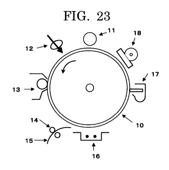
Fig. 23 is an explanatory, schematic view of an image forming
apparatus and an electrophotographic process of the present invention.
Fig. 24 is an explanatory, schematic view of a tandem full-color
image forming apparatus of the present invention.
Fig. 25 is an explanatory, schematic view of one exemplary
CA 02824648 2013-07-11
WO 2012/099181
PCT/JP2012/051012
process cartridge of the present invention.
Fig. 26 is a schematic front view of a characteristics tester used in
Examples.
Fig. 27 is a schematic side view of a characteristics tester used in
Examples.
Fig. 28A is a graph referred to for explaining a calculation method
for electrostatic capacity.
Fig. 28B is a graph referred to for explaining a calculation method
for electrostatic capacity.
Fig. 28C is a graph referred to for explaining a calculation method
for electrostatic capacity.
Description of Embodiments
(Electrophotographic photoconductor)
An electrophotographic photoconductor of the present invention
contains a conductive substrate and at least a photoconductive layer on
the conductive substrate, wherein the uppermost surface layer of the
photoconductive layer includes a three-dimensionally crosslinked film
formed through polymerization reaction among compounds each
containing a charge transporting compound and three or more
[(tetrahydro-2H-pyran-2-yl)oxy]methyl groups where the charge
transporting compound has one or more aromatic rings and the
[(tetrahydro-2H-pyran-2-ypoxy]methyl groups are bound to the aromatic
rings of the charge transporting compound (compounds each containing a
21
CA 02824648 2013-07-11
WO 2012/099181
PCT/JP2012/051012
charge transporting compound and three or more
Rtetrahydro-2H-pyran-2-ypoxylmethyl groups bound to one or more
aromatic rings of the charge transporting compound), and the
three-dimensionally crosslinked film has a dielectric constant of lower
than 3.5.
Here, the present inventors have found that the compounds each
containing a charge transporting compound and three or more
[(tetrahydro-2H-pyran-2-ypoxy]methyl groups bound to one or more
aromatic rings of the charge transporting compound react together in the
presence of an appropriate catalyst to form a three-dimensionally
crosslinked film that is insoluble to, for example, an organic solvent and
has a high crosslink density. The present invention is based on this
finding. In consideration of the infrared absorption spectra and mass
reduction before and after reaction, this reaction was found to be a
reaction in which some of the [(tetrahydro-2H-pyran-2-yl)oxy]methyl
groups were partially cleaved and eliminated.
The (tetrahydro-2H-pyran-2-y1) group has conventionally been
known as a protective group for a hydroxyl group. For example, this fact
is described in JP-A No. 2006-084711 (PTL 17). Although there have
been studied cured products through reaction among compounds having
this protective group and reactive species such as melamine, no reports
have been presented on formation of a crosslinked film using this
protective group alone.
Also, the term "protective group" leads generally to a concept
22
CA 02824648 2013-07-11
WO 2012/099181
PCT/JP2012/051012
where the protective group is removed to allow a target reaction to
proceed. Assuming that the reaction proceeds after the
[(tetrahydro-2H-pyran-2-yl)oxy]methyl groups have been changed to
methylol groups, the obtained three-dimensionally crosslinked film is the
same as a crosslinked film of a methylol compound. As a result of
studies, however, it has been found in the present invention that the
compound containing a charge transporting compound and three or more
[(tetrahydro-2H-pyran-2-ypoxy]methyl groups bound to one or more
aromatic rings thereof react together without the
[(tetrahydro-2H-pyran-2-ynoxy]methyl groups being changed to methylol
groups. Thus, the [(tetrahydro-2H-pyran-2-yl)oxy]methyl groups remain
as is in unreacted sites. As such, the
[(tetrahydro-2H-pyran-2-yl)oxy]methyl groups remaining in the structure
of the crosslinked film influence properties of the film. The
three-dimensionally crosslinked film of the present invention has an
advantages that it is smaller than a crosslinked cured product of a
methylol compound in terms of gas permeability; i.e., gas resistance.
Using the uppermost surface layer of a photoconductive layer, the
uppermost surface layer including a three-dimensionally crosslinked film
formed through polymerization reaction among the compounds each
containing a charge transporting compound and three or more
[(tetrahydro-2H-pyran-2-ypoxy]methyl groups bound to one or more
aromatic rings thereof and having a dielectric constant of lower than 3.5
can provide an electrophotographic photoconductor excellent in charging
23
CA 02824648 2013-07-11
WO 2012/099181
PCT/JP2012/051012
stability, NOx resistance, mechanical durability and environmental
stability. Also, the three-dimensionally crosslinked film is a cured
product of the charge transporting compound alone and thus exhibits
good charge transporting property. In addition, the three-dimensionally
crosslinked film appropriately contains electrically inactive sites that do
not directly contribute to charge transportation, such as the
[(tetrahydro-2H-pyran-2-ypoxy]methyl groups, and thus is excellent in
charging stability. Furthermore, the three-dimensionally crosslinked
film does not contain any polar group such as a hydroxyl group and thus
is excellent in environmental stability and gas resistance, capable of
forming a desired electrophotographic photoconductor.
The dielectric constant in the present invention is defined as
follows. Specifically, the dielectric constant is calculated from the
following equation (I) by using an electrostatic capacity (pF/cm2) and a
film thickness (p.m) of the photoconductive layer.
Notably, Cr denotes a dielectric constant, C denotes an
electrostatic capacity [F/m21, d denotes a film thickness [m], and Co is 8.85
x 10-12 [Final.
Cr = C x d/e0 Equation (I)
<Conductive substrate>
The conductive substrate is not particularly limited, so long as it
exhibits a volume resistivity of 1010 S-2-cm or less, and may be
appropriately selected depending on the intended purpose. Examples
thereof include coated products formed by coating, on film-form or
24
CA 02824648 2013-07-11
WO 2012/099181
PCT/JP2012/051012
cylindrical plastic or paper, a metal (e.g, aluminum, nickel, chromium,
nichrome, copper, gold, silver or platinum) or a metal oxide (e.g., tin oxide
or indium oxide) through vapor deposition or sputtering; and also include
an aluminum plate, an aluminum alloy plate, a nickel plate and a
stainless steel plate. Furthermore, there may be used tubes produced as
follows: the above metal plate is formed into a raw tube through extrusion,
pultrusion, etc. and then subjected to surface treatments such as cutting,
superfinishing and polishing. Also, an endless nickel belt or an endless
stainless-steel belt described in JP-A No. 52-36016 may be used as the
substrate.
Besides, the conductive substrate usable in the present invention
may be the above conductive substrates additionally provided with a
conductive layer formed through coating of a dispersion liquid of
conductive powder in an appropriate binder resin.
Examples of the conductive powder include carbon black,
acethylene black; powder of a metal such as aluminum, nickel, iron,
nichrome, copper, zinc or silver; and powder of a metal oxide such as
conductive tin oxide or ITO. Examples of the binder resin which is used
together with the conductive powder include thermoplastic resins,
thermosetting resins and photocurable resins such as polystyrene resins,
styrene-acrylonitrile copolymers, styrene-butadiene copolymers,
styrene -maleicanhydride copolymers, polyester resins, polyvinyl chloride
resins, vinyl chloride-vinyl acetate copolymers, polyvinyl acetate resins,
polyvinylidene chloride resins, polyarylate resins, phenoxy resins,
CA 02824648 2013-07-11
WO 2012/099181
PCT/JP2012/051012
polycarbonate resins, cellulose acetate resins, ethyl cellulose resins,
polyvinyl butyral resins, polyvinyl formal resins, polyvinyl toluene resins,
poly-N-vinylcarbazole, acrylic resins, silicone resins, epoxy resins,
melamine resins, urethane resins, phenol resins and alkyd resins.
Such a conductive layer may be formed through coating of a
dispersion liquid of the conductive powder and the binder resin in an
appropriate solvent (e.g., tetrahydrofuran, dichloromethane, methyl ethyl
ketone or toluene).
In addition, suitably used as the above substrate is a substrate
formed by providing an appropriate cylindrical support with, as a
conductive layer, a heat-shrinkable tubing containing the conductive
powder and a material such as polyvinyl chloride, polypropylene,
polyester, polystyrene, polyvinylidene chloride, polyethylene, chlorinated
rubber or Teflon (registered trademark).
<Photoconductive layer>
The photoconductive layer contains a charge generation layer, a
charge transport layer and a crosslinked charge transport layer in this
order; i.e., the charge transport layer is located between the charge
generation layer and the crosslinked charge transport layer. The
crosslinked charge transport layer is preferably the uppermost surface
layer of the photoconductive layer.
<<Uppermost surface layer (crosslinked charge transport layer)>>
The uppermost surface layer includes a three-dimensionally
crosslinked film formed through polymerization reaction among
26
CA 02824648 2013-07-11
WO 2012/099181
PCT/JP2012/051012
compounds each containing a charge transporting compound and three or
more [(tetrahydro-2H-pyran-2-yDoxy]methyl groups bound to one or more
aromatic rings thereof and having a dielectric constant of lower than 3.5.
The dielectric constant of the three-dimensionally crosslinked film
is preferably 2.5 or higher but lower than 3.5, more preferably 3.0 to 3.4.
The three-dimensionally crosslinked film is a structure formed as
follows. Specifically, the compounds each containing a charge
transporting compound and three or more
[(tetrahydro-2H-pyran-2-ypoxy]methyl groups bound to one or more
aromatic rings thereof bind with one another after some of the
[(tetrahydro-2H-pyran-2-yDoxy]methyl groups have partially been
cleaved and eliminated, to thereby form a macromolecule having a
three-dimensional network structure; and other of the
[(tetrahydro-2H-pyran-2-ypoxy]methyl groups remain as is.
Next will be described the compound containing a charge
transporting compound and three or more
[(tetrahydro-2H-pyran-2-yDoxy]methyl groups bound to one or more
aromatic rings thereof.
Many materials have conventionally been known as charge
transporting compounds. Most of these materials have aromatic rings.
For example, there is at least one aromatic ring in any of a triarylamine
structure, an aminobiphenyl structure, a benzidine structure, an
aminostilbene structure, a naphthalenetetracarboxylic acid diimide
structure and a benzylhydrazine structure. There can be used any of
27
CA 02824648 2013-07-11
WO 2012/099181
PCT/JP2012/051012
compounds each having any of these charge transporting compounds and
three or more [(tetrahydro-2H-pyran-2-y1)oxy]methyl groups, as
substituents, bound to one or more aromatic rings thereof.
The compound containing a charge transporting compound and
three or more [(tetrahydro-2H-pyran-2-yfloxylmethyl groups bound to one
or more aromatic rings thereof is preferably a compound represented by
the following General Formula (1).
CH20--0
1
(-0 Ari
1
)-0H2C-Ar3-N-Ar2-CH20-0 ( 1 )
In General Formula (1), An, Ar2 and Ar3 each denote a divalent
group of a C6-C18 aromatic hydrocarbon group which may have an alkyl
group as a substituent.
Although any of the compounds each containing the above charge
transporting compound and three or more
[(tetrahydro-2H-pyran-2-yl)oxylmethyl groups bound to one or more
aromatic rings thereof could form a three-dimensionally crosslinked film
through polymerization reaction, the compound represented by General
Formula (1) has a large amount of the
[(tetrahydro-2H-pyran-2-ypoxy]methyl groups relative to the molecular
weight thereof. Thus, this compound can form a three-dimensionally
crosslinked film having a high crosslink density, and can provide a
photoconductor having high hardness and high scratch resistance.
An, Ar2 and Ar3 in General Formula (1) each denote a divalent
28
CA 02824648 2013-07-11
WO 2012/099181
PCT/JP2012/051012
group of a C6-C18 aromatic hydrocarbon group which may have an alkyl
group as a substituent. Here, examples of the C6-C18 aromatic
hydrocarbon group include benzene, naphthalene, fluorene, phenanthrene,
anthracene, pyrene and biphenyl. Examples of the alkyl group these
may have as a substituent include linear or branched aliphatic alkyl
groups such as methyl, ethyl, propyl, butyl, pentyl, hexyl, heptyl and
octyl.
Also, the compound containing a charge transporting compound
and three or more [(tetrahydro-2H-pyran-2-ypoxy]methyl groups bound to
one or more aromatic rings thereof is preferably a compound represented
by the following General Formula (2).
c3-0H2C CH20¨Q
1 1
Ar8 Ar5 ( 2 )
c3-0H2C-Ar9-N-Ar7-X1-Ar4-N-Ar6-C H2
0
In General Formula (2), Xi denotes a C1-C4 alkylene group, a
C2-C6 alkylidene group, a divalent group formed of two C2-C6 alkylidene
groups bonded together via a phenylene group, or an oxygen atom, and
Arl, Ar5, Ars, Ar7, Ars and Ar9 each denote a divalent group of a C6-C12
aromatic hydrocarbon group which may have an alkyl group as a
substituent.
In General Formula (2), examples of the C6-C12 aromatic
hydrocarbon group in the divalent groups denoted by Ar4, Ar5, Ars, Ar7,
Ars and Ar9 include the same as exemplified in the divalent groups
denoted by An, Ar2 and Ar3 in General Formula (1).
29
CA 02824648 2013-07-11
WO 2012/099181
PC17,1P2012/051012
Examples of the C1-C4 alkylene group denoted by Xi in General
Formula (2) include linear or branched alkylene groups such as
methylene, ethylene, propylene and butylene.
Examples of the C2-C6 alkylidene group denoted by Xi in General
Formula (2) include 1,1-ethylidene, 1,1-propylidene, 2,2-propylidene,
1,1-butylidene, 2,2-butylidene, 3,3-pentanylidene and 3,3-hexanylidene.
Examples of the divalent group Xi formed of two C2-C6 alkylidene
groups bonded together via a phenylene group in General Formula (2)
include the following groups:
Me Me Me Me
I I
¨1 I I I¨(0)¨ 6¨ ¨C-- (a C¨
Me Me = Me Me
where Me denotes a methyl group.
The compound represented by General Formula (2) contains a
charge transporting compound and three or more
[(tetrahydro-2H-pyran-2-yl)oxylmethyl groups bound to aromatic rings
thereof, and also contains a nonconjugated linking group denoted by Xi
and thus has an appropriate molecular mobility. Through
polymerization reaction, this compound can easily form a
three-dimensionally crosslinked film in which some of the
[(tetrahydro-2H-pyran-2-ypoxy]methyl groups remain as is. The formed
three-dimensionally crosslinked film achieves a favorable balance
between hardness and elasticity, making it possible to form a stiff surface
protective layer excellent in scratch resistance and abrasion resistance.
CA 02824648 2013-07-11
WO 2012/099181
PCT/JP2012/051012
Furthermore, by virtue of the structure of Xi, the molecule has a
relatively high oxidation potential not to be easily oxidized. Thus, this is
relatively stable when exposed to oxidative gas such as ozone gas or NOx
gas, making it possible to provide a photoconductor having excellent gas
resistance.
When the three-dimensionally crosslinked film is insoluble to a
solvent, it exhibits remarkably excellent mechanical properties. The
compound containing a charge transporting compound and three or more
[(tetrahydro-2H-pyran-2-ylloxy]methyl groups bound to one or more
aromatic rings thereof dissolves in tetrahydrofuran in a large amount.
Once this compounds react and bond with one another to form a
three-dimensionally network structure, the resultant product no longer
dissolves in tetrahydrofuran or any other solvents.
Thus, the fact that the three-dimensionally crosslinked film is
insoluble to tetrahydrofuran means that a macromolecule has been
formed in the surface of the photoconductor and the obtained
photoconductor exhibits high mechanical properties (mechanical
durability).
Here, the "being insoluble" means a state where the film does not
disappear even when immersed in tetrahydrofuran.
More preferably, this state is a state where even when the film is
rubbed with a swab, etc. soaked in tetrahydrofuran, there is no trace left
in the film.
When the film is allowed to be insoluble to a solvent, foreign
31
CA 02824648 2013-07-11
WO 2012/099181 PCT/JP2012/051012
matter can be prevented from adhering to the photoconductor, and also
the photoconductor surface can be prevented from being scratched due to
adhesion of the foreign matter.
Also, the compound containing a charge transporting compound
and three or more [(tetrahydro-2H-pyran-2-yDoxylmethyl groups bound to
one or more aromatic rings thereof is preferably a compound represented
by the following General Formula (3).
c..0?_
OH2C CH20--
I I
Aril Ar12 ( 3 )
/-R i 1
\__/-0CHrAria-N-Yr-N-Ari3--CH20-b
wherein Yi denotes a divalent group of phenyl, biphenyl,
terphenyl, stilbene, distyrylbenzene or a fused polycyclic aromatic
hydrocarbon, and Arlo, Arii, Ar12 and Ar13 each denote a divalent group of
a C6-C18 aromatic hydrocarbon which may have an alkyl group as a
substituent.
In General Formula (3), the groups denoted by Arlo, Aril, Ar12
and Arm may be the same as those denoted by An, Ar2 and Ar3 in General
Formula (1).
In General Formula (3), Yi denotes a divalent group of phenyl,
biphenyl, terphenyl, stilbene, distyrylbenzene or a fused polycyclic
aromatic hydrocarbon. Examples of the fused polycyclic aromatic
hydrocarbon include naphthalene, phenanthrene, anthracene and pyrene.
The compound represented by General Formula (3) contains a
charge transporting compound and three or more
32
CA 02824648 2013-07-11
WO 2012/099181
PCT/JP2012/051012
[(tetrahydro-2H-pyran-2-yDoxy]nethyl groups bound to aromatic rings
thereof, and easily forms through polymerization reaction a
three-dimensionally crosslinked film in which some of the
Rtetrahydro-2H-pyran-2-ypoxylmethyl groups remain. This compound
has a diamine structure containing as a linking structure a specific
aromatic hydrocarbon structure denoted by Yi. Thus, charges can move
in the molecule thereof, making it possible to form a crosslinked
protective layer having a high hole mobility. Therefore, even in cases
where a process starting from photo-writing of a photoconductor to
development thereof is performed for a short period of time (e.g.,
high-speed printing or printing using a drum with a small diameter), it is
possible to stably print out high-quality images.
Also, the compound containing a charge transporting compound
and three or more [(tetrahydro-2H-pyran-2-ypoxy]methyl groups bound to
one or more aromatic rings thereof is preferably a compound represented
by the following General Formula (4).
'Rill 4H20--0
(-3-0H2C-O-N R2] m
4R3]
n ( 4 )
CH20-0
wherein R1, R2 and R3, which may be the same or different, each
denote a hydrogen atom, a methyl group or an ethyl group; and 1, n and m
each denote an integer of 1 to 4.
33
CA 02824648 2013-07-11
WO 2012/099181
PCT/JP2012/051012
The compound represented by General Formula (4) is particularly
excellent among the compounds represented by General Formula (1), and
has particularly high polymerization reactivity. Although the
polymerization reaction among the
Rtetrahydro-2H-pyran-2-ypoxylmethyl groups is still unclear, when the
aromatic rings having the Rtetrahydro-2H-pyran-2-yDoxylmethyl groups
are benzene rings having a tertiary amino group, the polymerization
reaction proceeds at the highest rate. As a result, it is possible to form a
crosslinked protective layer (crosslinked charge transport layer) having
higher crosslink density.
Also, the compound containing a charge transporting compound
and three or more [(tetrahydro-2H-pyran-2-yl)oxy]methyl groups bound to
one or more aromatic rings thereof is preferably a compound represented
by the following General Formula (5).
Q c_c
=
0 I R.GN-Q-X2-0-N R8] s t-\
( 5 )
I, -DeoR91
P` iRsi t
q
b b
In General Formula (5), X2 denotes -CH2-, -CH2CH2-,
-C(CH3)2-Ph-C(CH3)2-, -C(CH2)5- or -0- (where Ph denotes a phenyl
group); R4, R5, R6, R7, R8 and Its, which may be the same or different, each
34
CA 02824648 2013-07-11
WO 2012/099181 PCT/JP2012/051012
denote a hydrogen atom, a methyl group or an ethyl group; and o, p, q, r,
s and t each denote an integer of 1 to 4.
The compound represented by General Formula (5) is particularly
excellent among the compounds represented by General Formula (2), and
has high polymerization reactivity. This compound has the same
features as those of the compound represented by General Formula (2),
making it possible to form a three-dimensionally crosslinked film
(crosslinked charge transport layer) having a high crosslink density.
Also, the compound containing a charge transporting compound
and three or more [(tetrahydro-2H-pyran-2-ypoxylmethyl groups bound to
one or more aromatic rings thereof is preferably a compound represented
by the following General Formula (6).
0 0
u
Cdt-R12],õ,
(6 )
V beti31
In General Formula (6), Y2 denotes a divalent group of phenyl,
naphthalene, biphenyl, terphenyl or styryl; Rio, Rii, R12 and R13, which
may be the same or different, each denote a hydrogen atom, a methyl
group or an ethyl group; and u, v, w and z each denote an integer of 1 to
4.
The compound represented by General Formula (6) is particularly
CA 02824648 2013-07-11
WO 2012/099181
PCT/JP2012/051012
excellent among the compounds represented by General Formula (3), and
has high polymerization reactivity. This compound has the same
features as those of the compound represented by General Formula (3),
making it possible to form a three-dimensionally crosslinked film
(crosslinked charge transport layer) having a high crosslink density.
Among them, the compounds represented by General Formulas
(1) to (6) have the above-described features and are used preferably. In
particular, the compounds represented by General Formulas (4) to (6)
have high crosslinking reaction rate and are used more preferably.
Specific examples of the compound containing a charge
transporting compound and three or more
[(tetrahydro-2H-pyran-2-yl)oxy]methyl groups bound to one or more
aromatic rings thereof will be given below; however, the present invention
should not be construed as being limited thereto. In the following
compounds, Me denotes a methyl group and Et denotes an ethyl group.
36
CA 02824648 2013-07-11
WO 2012/099181
PCT/JP2012/051012
Table 1-1
Compd.
No. Chemical Structure
O-CH 0 0 0CHrOt
1
CHr
Me
C3-0-CH 0 0 0
2
CHrO¨c.
C5-0-CH 0 0 0 0 CH2-0-
3
CHr
C51-0-CH 0 0 CHr0-
4
CHrO¨c.
Me
CC3-0-CH 0 0 CH2-0-
Me *Me
C5-0-CH CO CHrO¨c
6
(tri
CHr0¨c.
37
CA 02824648 2013-07-11
WO 2012/099181
PCT/JP2012/051012
Table 1-2
Compd.
No. Chemical Structure
M
0
0-0-CHe MeC> CH2-0¨c
7
C3-0-CH 0 0 CH 0 CHr0¨c.
8
(jY1
CH2-0¨b
Me Me
C3-0-CH 40 0 CH 0 0 CHr0¨c_
9
(1)
Me
0
0-0-CH 40 C> CH Me
0 0 CH2-0¨b
1 0
me,0
CH2-Cs¨c CHrO¨c
Me Me
C3-0-CH C> C> CH C> CH2-0--
1 1
CI)
Me Me Me Me
C3-0-CH 0 CH CI 0 CH2-0¨c
12
38
CA 02824648 2013-07-11
WO 2012/099181
PCT/JP2012/051012
Table 1-3
Compd.
No. Chemical Structure
E Et
C3-0-CH C> 0 CH CO 0 CHrO-c..
13 C:Ld Et Et )
CH2-0- CH2-0-
Me Me Me Me
C3-0-CH 0 0 CH 0 C> CH2-0-
1 4
00
M-
CH2- - M CH2-0-
0-0-CH 0 0 = 0 0 CH2-0-
1 5
CI)0
CH2-0-b CH2-0--
Me Me
C3-0-CH 0 C> = 0 C> CHr0--c_
16
CH2-0-- CH2-0--
Me Me
C5-0-CH C> 0 = 0 C> CHrO-b
1 7
M M-
0 0
CH2-O-c_ CH2-0-b
I
00-0-CH Et
CO 0 ? 0 0 CH2-0-b
18
ClID Et
0
CH2-0-c. CH2-0-
39
CA 02824648 2013-07-11
WO 2012/099181 PCT/JP2012/051012
Table 1-4
Compd.
Chemical Structure
No.
C3-0-CH 0 C> CH2CH C> 0 CH2-0--
1 9
(I) C12)
CH2-0-c. CH2-0-c
Me Me
C3-0-CH 0 C> CH2CH C> C> CH2-0-
2 0
0 0
M M-
CH2-0- CH2-0-
CH
0-0-CH 0 0 I 0 0 CH2-0-c.
2 1
Cf)I
CH2CH2CH3
CH2-0-c. CH2-0--
CH3
C5-0-CH 0 0 I 0 0 CH2-0-c.
1
2 2 CH2CH-CH3
I
0 c. CH3
CH2-o_ CHrO-c
CH3 CH3
0-0-CH 10 ()COI C) 0 CH2-0-c
C
2 3 CH3 I
CH3 0
CH2-0- CH2-0--
Me CH3 CH3 Me
C3-0-CH 0 0 I C> 1 C> 0 CH2-0-
2 4
(Ld CH3 I
CH3 0
CH2-0- cH2-0--
CA 02824648 2013-07-11
WO 2012/099181 PCT/JP2012/051012
Table 1-5
Compd.
Chemical Structure
No.
Me CH3 CH3 Me
C3-0-CH 0 CO 1 CI
2 5
0 CH3 CH3 0
M- M
CH2-0- CH2-0--c.
C3-0-CH 0 0 CO C> CHr0--c.
26 0 IP 0
CH2-0- CH2-0-
Me Me
C3-0-CH CO 0 0 CI CH2-0--
2 7
CI) 0
CHr0-- CH2-0-
Me Me
C5-0-CH 0 0 0 0 CHT-0-
2 8
M* M* 0 IIP
0
CH2-Cs-C CH2-0-
C3-0-CH C>
29 0 04 0 0
c3_0-CH2 CHrO'tJ Me
C3-0-CH Cp 0 0 0 CH2-0-c.
0 0 0 0
C)--0-CH2 CH2-0-
41
CA 02824648 2013-07-11
WO 2012/099181
PCT/JP2012/051012
Table 1-6
Compd.
Chemical Structure
No.
cOy0-CH2 CHr0-
3 1 0 0 0 0
0_0 2 0
0
O-CH CH2-0-
C3-0-CH 0 0 0 0 CH2-0-c.
32
o
0 0 CLri
0-CH2 CH2-0-c_.
Me Me
C5-0-CH 0 CO 0 CO CHr0--
3 3
0 p.
0
C3_0-CH2 CH2-0-
(5_
0-CH2 Me Me CH2-0-
3 4 0 0 0 0
0 0c3_
0-CH2 CH2-0-c -)
Me Me
C3-0-CH C> CO 0 0 CHr0-
3 5
5 C-0-CH2 CH20---
Me Me Me Me
00-0-CH 00 0 0 0 CH2-0-
36
0 Cli)
0-0-CH2 CH2-0-
42
CA 02824648 2013-07-11
WO 2012/099181 PCT/JP2012/051012
Table 1-7
Compd.
Chemical Structure
No.
Me Me
09-0-CH 0 0 0 0 CHr0¨
\L) 0H2Me M
3 7
Me Me Me Me
C3-0-CH 0 0 0 0 CHr0-
3 8
Me M-
o-CH2
C3-0-CH 0 CFC C> CHr0¨c.
39
CHr0¨
tJ
Me Me
0
0-0-CH 0 0 CFC 0 0 CH2-0-
4 0
CLr)
CHrO¨c. CHrO¨c
Me Me
0
0-0-CH C> CFC C> CHr0-
4 1
M-
(3-0-CH 40 Cs 0 0 0 CHr0-
4 2
(J-.O CH2-0-
43
CA 02824648 2013-07-11
WO 2012/099181
PCT/JP2012/051012
Table 1-8
Compd.
Chemical Structure
No.
Me
0
i-O-CH Me 0 CO 0 0 CH2-0-
4 3
CI
cOy Me M
0-CH2 CH2-0-c
C3-0-CH 0 0 0 0 CH2-0-c_
44
0
0-0-CH2 CH2-0-c
0
0-0-CH CO C>
C1-0-CH2
(1-0Hz
CH20-Q
00 46
0 0
LA-120-0
The above-described compound containing a charge transporting
compound and three or more [(tetrahydro-2H-pyran-2-ynoxy]methyl
5 groups bound to one or more aromatic rings thereof is a novel compound
and can be produced by, for example, the following method.
-Synthesis method for the compound containing a charge transporting
compound and three or more Rtetrahydro-2H-pyran-2-ypoxylmethyl
groups bound to one or more aromatic rings thereof-
10 --First synthesis method--
44
CA 02824648 2013-07-11
WO 2012/099181
PCT/JP2012/051012
In a first synthesis method, three or more aromatic rings of a
charge transporting compound are formylated to form formyl groups; the
thus-formed formyl groups are then reduced to form methylol groups; and
the thus-formed methylol groups are then reacted with
3,4-dihydro-2H-pyran to form [(tetrahydro-2H-pyran-2-ypoxylmethyl
groups on the charge transporting compound.
In one employable method, an aldehyde compound is synthesized
according to the below-described procedure; the obtained aldehyde
compound is reacted with a reducing agent such as sodium borohydride to
synthesize a methylol compound; the obtained methylol compound is
reacted with dihydro-2H-pyran to obtain a compound containing a charge
transporting compound and [(tetrahydro-2H-pyran-2-yDoxylmethyl
groups bound to one or more aromatic rings thereof. Specifically, this
compound can easily be synthesized in the following production method.
--Second synthesis method--
A second synthesis method is a method using as a starting
material a compound having aromatic rings each having a halogen atom
and a methylol group. In this method, the methylol groups are reacted
with 3,4-dihydro-2H-pyran in the presence of an acid catalyst to
synthesize an aromatic compound having halogen atoms and
[(tetrahydro-2H-pyran-2-ypoxylmethyl groups; and the thus-synthesized
aromatic compound is coupled with an amine compound to synthesize the
charge transporting compound.
Depending on the number of amines or on whether the amine is
CA 02824648 2013-07-11
WO 2012/099181
PCT/JP2012/051012
primary, secondary or tertiary, it is possible to introduce many
[(tetrahydro-2H-pyran-2-yDoxylmethyl groups at one time. When the
halogen is iodine (i.e., iodine compound), the amine compound can be
coupled through Ullmann reaction with the halogen (iodine) compound
having the Rtetrahydro-2H-pyran-2-yDoxylmethyl groups. When the
halogen is chlorine (i.e., chlorine compound) or bromine (i.e., bromine
compound), the amine compound can be coupled therewith through, for
example, Suzuki-Miyaura reaction using a palladium catalyst.
---Synthesis of aldehyde compound--
1 0 As shown
in the following reaction formula, a charge transporting
compound, serving as a starting material, can be formylated by a
conventionally known method (e.g., Vilsmeier reaction) to synthesize an
aldehyde compound. For example, this formylation can be performed as
described in JP-B No. 3943522.
[Art
0 ]m --0- [Ar¨N 0 HO]
n- n m
Specifically, it is effective that this formylation method is a
method using zinc chloride/phosphorus
oxychloride/dimethylformaldehyde. However, the synthesis method for
the aldehyde compound, which is an intermediate used in the present
invention, should not be construed as being limited thereto. Specific
synthesis examples will be given as the below-described Synthesis
Examples.
46
CA 02824648 2013-07-11
WO 2012/099181
PCT/JP2012/051012
---Synthesis of methylol compound---
As shown in the following reaction formula, the aldehyde
compound, serving as a production intermediate, can be reduced by a
conventionally known method to synthesize a methylol compound.
[Ar
0 HO] --I- [ArtN 0 CH2OH 1
n m n m
Specifically, it is effective that this reduction method is a method
using sodium borohydride. However, the synthesis method for the
methylol compound should not be construed as being limited thereto.
Specific synthesis examples will be given in the below-described
Examples.
---Synthesis of the compound containing a charge transporting compound
and [(tetrahydro-2H-pyran-2-yDoxylmethyl groups bound to one or more
aromatic rings thereof [1]¨
As shown in the following reaction formula, the methylol
compound, serving as a production intermediate, can be added with
3,4-dihydro-2H-pyran in the presence of a catalyst to synthesize the
compound containing a charge transporting compound and
[(tetrahydro-2H-pyran-2-yDoxy]methyl groups bound to one or more
aromatic rings thereof.
0
[Ar¨ H2oHl m --..- [Art 0 CH20¨ ]
- n n m
47
CA 02824648 2013-07-11
WO 2012/099181
PCT/JP2012/051012
Specifically, it is effective that this synthesis method is a method
using dihydro-2H-pyran. However, the synthesis method for the
compound of the present invention containing a charge transporting
compound and [(tetrahydro-2H-pyran-2-ypoxy]methyl groups bound to
one or more aromatic rings thereof should not be construed as being
limited thereto. Specific synthesis examples will be given in the
below-described Examples.
----Synthesis of an intermediate compound having a
[(tetrahydro-2H-pyran-2-ypoxy]methyl group--
The synthesis method for an intermediate compound having a
[(tetrahydro-2H-pyran-2-yl)oxy]methyl group is, for example, a method in
which a compound having an aromatic ring with a halogen atom and a
methylol group is used as a starting material; and the methylol group is
reacted with 3,4-dihydro-2H-pyran in the presence of an acid catalyst to
synthesize an intermediate compound having a halogen atom and a
[(tetrahydro-2H-pyran-2-yDoxy]methyl group.
X 0 CH2OH -PP X 0 C H 2 0-0
In this reaction formula, X denotes halogen.
---Synthesis of the compound containing a charge transporting compound
and [(tetrahydro-2H-pyran-2-ypoxy]methyl groups bound to one or more
aromatic rings thereof [2]---
As shown in the following reaction formula, an amine compound
and a halogen compound with a tetrahydropyranyl group, serving as
48
CA 02824648 2013-07-11
WO 2012/099181
PCT/JP2012/051012
product intermediates, can be used to synthesize, with a conventionally
known method, the compound containing a charge transporting
compound and [(tetrahydro-2H-pyran-2-yDoxy]methyl groups bound to
one or more aromatic rings thereof.
Ar¨NH2 X ED CH20--0 --- Ar¨N ED CH20-0
2
H2N-Ar-NH2 + X-0-CH20-0 - [ C3-0H2C-0-N--Ar 0 1120-0 1
2 2
Specifically, it is effective that this synthesis method is a method
using, for example, Ullmann reaction. However, the synthesis method
for the compound of the present invention containing a charge
transporting compound and Rtetrahydro-2H-pyran-2-yDoxylmethyl
groups bound to one or more aromatic rings thereof should not be
construed as being limited thereto. Specific synthesis examples will be
given in the below-described Examples.
-Polymerization reaction (reaction mode)-
Although there has not been elucidated the reaction in which
some of the [(tetrahydro-2H-pyran-2-yDoxylmethyl groups are partially
cleaved and eliminated, the polymerization reaction therebetween is not a
single reaction but a reaction in which a plurality of reactions as shown
below competitively proceed to link the compounds together.
The reaction mode is shown below.
--Reaction mode 1--
49
CA 02824648 2013-07-11
WO 2012/099181 PCT/JP2012/051012
Ar-CH2-0- + (-5-0-CH2- Ar Ar- C Hz- 0- C
H2- Ar
In the above reaction formula, Ar denotes any aromatic ring of the
charge transporting compound used in the present invention.
In this reaction, the tetrahydro-2H-pyran-2-y1 group of one
Rtetrahydro-2H-pyran-2-ynoxylmethyl group is cleaved and eliminated;
and then, while the (tetrahydro-2H-pyran-2-ypoxy group of the other
[(tetrahydro-2H-pyran-2-ypoxy]methyl group is being cleaved and
eliminated, a dimethylene ether bond is formed therebetween.
--Reaction mode 2--
Ar-CH2- cOy 0- CH2- Ar Ar-CH2- CH2- Ar
In the above reaction formula, Ar denotes any aromatic ring of the
charge transporting compound used in the present invention.
In this reaction, while the (tetrahydro-2H-pyran-2-ypoxy groups
of both the [(tetrahydro-2H-pyran-2-ypoxy]methyl groups are being
cleaved and eliminated, an ethylene bond is formed therebetween.
--Reaction mode 3--
Ar-CH2-0- C5-0-CH2-Ar Ar-CH2-Ar-CH2-0-
In the above reaction formula, Ar denotes any aromatic ring of the
charge transporting compound used in the present invention.
In this reaction, while the (tetrahydro-2H-pyran-2-ypoxy group of
one [(tetrahydro-2H-pyran-2-ypoxy]methyl group is being cleaved and
CA 02824648 2013-07-11
WO 2012/099181
PCT/JP2012/051012
eliminated, the one Rtetrahydro-2H-pyran-2-ypoxylmethyl group binds
with the aromatic ring of the other
[(tetrahydro-2H-pyran-2-ypoxylmethyl group to form a methylene bond
therebetween.
Through combination of at least these reactions, the
[(tetrahydro-2H-pyran-2-ypoxylmethyl groups are polymerized so as to
have various bonds, to thereby form a macromolecule having a
three-dimensional network structure.
The (tetrahydro-2H-pyran-2-yl)oxy group is generally known as a
protective group of a hydroxyl group. In the three-dimensionally
crosslinked film (cured film) of the present invention, the
[(tetrahydro-2H-pyran-2-yDoxylmethyl groups remain. Thus,
presumably, deprotection reaction does not occur. In other words, the
[(tetrahydro-2H-pyran-2-ypoxy]methyl group is not hydrolyzed to change
into a methylol group.
In addition, the (tetrahydro-2H-pyran-2-yl)oxy group has a low
polarity and thus, the unreacted, remaining
(tetrahydro-2H-pyran-2-yDoxy group does not adversely affect electrical
characteristics or image quality.
The polymerization reaction tends to form a film having severe
distortion. However, relatively bulky
[(tetrahydro-2H-pyran-2-ypoxylmethyl groups remaining have an effect of
reducing such distortion, and also can be expected to compensate
molecular spaces formed through distortion, making it possible to form a
51
CA 02824648 2013-07-11
WO 2012/099181
PCT/JP2012/051012
film having low gas permeability and higher stiffness; i.e., lower
brittleness.
It is possible to desirably change the amount of the
[(tetrahydro-2H-pyran-2-yDoxy[methyl groups reacted or unreacted
(remaining) in the molecule, in order to adjust the structure of the charge
transporting compound and obtain the desired film properties. However,
when the amount of the [(tetrahydro-2H-pyran-2-yl)oxy]methyl groups
remaining is too small, the formed film involves severe distortion and
brittleness, and is not suitable to a long-service-life photoconductor.
Meanwhile, it is necessary to increase the reaction temperature, in order
to increase the amount of the [(tetrahydro-2H-pyran-2-yl)oxylmethyl
groups reacted. In this case, the heat degrades photoconductivity of the
formed photoconductor, leading to problems such as decrease in
sensitivity and increase in residual potential. When the amount of the
Rtetrahydro-2H-pyran-2-yl)oxylmethyl groups remaining is too large, the
formed film decreases in crosslink density and in some cases, dissolves in
an organic solvent; i.e., poorly crosslinked state. As a result, it does not
exhibit excellent mechanical properties attributed to the
three-dimensionally crosslinked film. Thus, it is preferred to select such
curing conditions as to give a film having both favorable mechanical
properties and favorable electrostatic properties.
The three-dimensionally crosslinked film in the
electrophotographic photoconductor of the present invention is preferably
obtained through polymerization reaction among the compounds each
52
CA 02824648 2013-07-11
WO 2012/099181
PCT/JP2012/051012
containing a charge transporting compound and three or more
Rtetrahydro-2H-pyran-2-ypoxylmethyl groups bound to the aromatic
rings thereof in the presence of a curing catalyst.
Use of the curing catalyst under heating allows the
polymerization reaction to proceed at a practical rate, making it possible
to form the uppermost surface layer excellent in surface smoothness.
When the surface smoothness is considerably degraded, cleanability of
toner particles are also degraded to cause formation of abnormal images;
i.e., inhibit high-quality printing. When an appropriate curing catalyst
is used under heating at an appropriate temperature, it is possible to
form a three-dimensionally crosslinked film excellent in surface
smoothness. When this three-dimensionally crosslinked film is used as
the uppermost surface layer of the photoconductive layer of the
electrophotographic photoconductor, the formed electrophotographic
photoconductor can form (print) high-quality images for a long period of
time.
-Formation method for three-dimensionally crosslinked film-
The three-dimensionally crosslinked film can be formed as follows.
Specifically, a coating liquid containing the curing catalyst and the
compound containing a charge transporting compound and three or more
[(tetrahydro-2H-pyran-2-yDoxylmethyl groups bound to one or more
aromatic rings thereof is prepared or diluted optionally using, for
example, a solvent; and the obtained coating liquid is coated on the
photoconductor surface and heated and dried to perform polymerization.
53
CA 02824648 2013-07-11
WO 2012/099181
PCT/JP2012/051012
In an alternative manner, two or more types of the compound containing
a charge transporting compound and three or more
Rtetrahydro-2H-pyran-2-ypoxylmethyl groups bound to one or more
aromatic rings thereof are used in combination and mixed together, and
the resultant mixture is used to form the three-dimensionally crosslinked
film in the same manner as described above.
The temperature for heating the coating liquid is preferably 80 C
to 180 C, more preferably 100 C to 160 C. Since the reaction rate can
change depending on the type or amount of a catalyst used, the heating
temperature may desirably be determined in consideration of the
formulation of the coating liquid. Although, the reaction rate becomes
higher with increasing the heating temperature, an extreme increase in
crosslink density leads to a decrease in charge transporting property
whereby the formed photoconductor is increased in exposed-area
potential and decreased in sensitivity. In addition, the other layers of
the photoconductor are increasingly affected due to heating, easily
degrading the properties of the formed photoconductor. When the
heating temperature is too low, the reaction rate is also low and as a
result, a sufficient crosslink density cannot be achieved even when
performing the reaction for a long period of time.
The curing catalyst is preferably an acid compound, more
preferably an organic sulfonic acid, an organic sulfonic acid derivative, etc.
Examples of the organic sulfonic acid include p-toluenesulfonic acid,
naphthalenesulfonic acid and dodecylbenzenesulfonic acid. Further
54
CA 02824648 2013-07-11
WO 2012/099181
PCT/JP2012/051012
examples include organic sulfonic acid salts, and so-called thermally
latent compounds showing acidity at a certain temperature or higher.
Examples of the thermally latent compound include
thermally latent proton acid catalysts blocked with an amine such as
NACURE2500, NACURE5225, NACURE5543 or NACURE5925 (these
products are of King Industries, Inc.), SI-60 (product of Sanshin Chemical
Industry Co.) and ADEKAOPTOMER SP-300 (product of ADEKA
CORPORATION).
The above catalyst is added to the coating liquid in an amount
(solid content concentration) of about 0.02% by mass to about 5% by mass.
When an acid such as p-toluenesulfonic acid is used alone, an amount of
about 0.02% by mass to about 0.4% by mass is enough. When the
amount is too large, the coating liquid is increased in acidity to cause
corrosion of coating apparatus, etc., which is not preferred. In contrast,
use of the thermally latent compound does not involve problems such as
corrosion at the step of coating the coating liquid and thus, it is possible
to increase the amount of the thermally latent compound. However, the
remaining amine compound used as the blocking agent adversely affects
the properties of the photoconductor such as residual potential. Thus,
use of the thermally latent compound in an extremely large amount is not
preferred. Since the thermally latent compound contains an acid in a
smaller amount in the case of the acid alone, the amount of the thermally
latent compound (catalyst) is properly 0.2% by mass to 2% by mass.
When the heating/drying temperature and time are appropriately
CA 02824648 2013-07-11
WO 2012/099181
PCT/JP2012/051012
selected considering the type or amount of a catalyst as described above,
it is possible to form three-dimensionally crosslinked films of the present
invention having various crosslink densities.
Examples of the solvent include alcohols such as methanol,
ethanol, propanol and butanol; ketons such as acetone, methyl ethyl
ketone, methyl isobutyl ketone and cyclohexanone; esters such as ethyl
acetate and butyl acetate; ethers such as tetrahydrofuran,
methyltetrahydrofuran, dioxane, propylether, diethylene glycol dimethyl
ether and propylene glycol-l-monomethyl ehter-2-acetate;
halogen-containing compounds such as dichloromethane, dichloroethane,
trichloroethane and chlorobenzene; aromatic compounds such as benzene,
toluene and xylene; and cellosolves such as methyl cellosolve, ethyl
cellosolve and cellosolve acetate. These solvents may be used alone or in
combination. The dilution rate by the solvent may be appropriately
determined depending on the dissolvability of the composition, the
coating method employed and/or the thickness of an intended film. The
coating of the coating liquid can be performed by, for example, a dip
coating method, a spray coating method, a bead coating method or a ring
coating method.
If necessary, the coating liquid may further contain an additive
such as a leveling agent or an antioxidant. Examples of the leveling
agent include silicone oils such as dimethylsilicone oil and
methylphenylsilicone oil; and polymers and oligomers each having a
perfiuoroalkyl group in the side chain thereof. The amount of the
56
CA 02824648 2013-07-11
WO 2012/099181
PCT/JP2012/051012
leveling agent is preferably 1% by mass or less relative to the total solid
content of the coating liquid. The antioxidant can suitably be used.
Examples of the antioxidant include conventionally known compounds
such as phenol compounds, paraphenylenediamines, hydroquinones,
organic sulfur compounds, organic phosphorus compounds and hindered
amines. The antioxidant is effective for stabilizing electrostatic
properties during repetitive use. The amount of the antioxidant is
preferably 1% by mass or less relative to the total solid content of the
coating liquid.
Furthermore, the coating liquid may contain a filler in order for
the formed film to be increased in abrasion resistance. The filler is
classified into organic filler materials and inorganic filler materials.
Examples of the organic filler materials include fluorine resin powder
such as polytetrafluoroethylene, silicone resin powder and a-carbon
powder. Examples of the inorganic filler materials include powders of
metals such as copper, tin, aluminum and indium; metal oxides such as
silica, tin oxide, zinc oxide, titanium oxide, alumina, zirconium oxide,
indium oxide, antimony oxide, bismuth oxide, calcium oxide, tin oxide
doped with antimony, and indium oxide doped with tin; and inorganic
materials such as potassium titanate and boron nitride. Among them,
use of inorganic materials is advantageous from the viewpoint of
increasing abrasion resistance, since they have higher hardness. In
particular, a-type alumina is useful from the viewpoint of increasing
abrasion resistance, since it has high insulating property, high thermal
57
CA 02824648 2013-07-11
WO 2012/099181
PCT/JP2012/051012
stability, and a hexagonal close-packed structure exhibiting high abrasion
resistance.
Moreover, the filler can be surface-treated with at least one
surface treating agent. The filler is preferably surface-treated therewith
since its dispersibility increases. Decrease in dispersibility of the filler
causes not only an increase in residual potential but also a decrease in
transparency of the coated film, formation of defects in the coated films,
and a decrease in abrasion resistance, potentially leading to severe
problems that inhibit high durability or high quality image formation.
The surface treating agent may be any conventionally-used
surface treating agent, but preferably used is a surface treating agent
able to maintain the insulating property of the filler. From the
viewpoints of improving filler dispersibility and preventing image blur,
such surface treating agent is more preferably a titanate coupling agent,
an aluminum coupling agent, a zircoaluminate coupling agent, a higher
fatty acid, mixtures containing these agents or acids and a silane coupling
agent; A1203, Ti02, Zr02, silicone, aluminum stearate and mixtures
thereof. A treatment with a silane coupling agent alone causes a
considerable degree of image blur, while a treatment with the mixture
containing the above surface treating agent and a silane coupling agent
may suppress such disadvantageous effect caused by the silane coupling
agent.
The amount of the surface treating agent varies with the average
primary particle diameter of the filler, but is preferably 3% by mass to
58
CA 02824648 2013-07-11
WO 2012/099181
PCT/JP2012/051012
30% by mass, more preferably 5% by mass to 20% by mass. When the
surface treating agent is less than the lower limit, it cannot exhibit an
effect of dispersing the filler. Whereas when the surface treating agent
is too large, it causes a considerable increase in residual potential. Also,
the average primary particle diameter of the filler is preferably 0.01 pm
to 0.5 pm from the viewpoint of improving optical transmittance and
abrasion resistance. When the average primary particle diameter of the
filler is less than 0.01 pm, abrasion resistance, dispersibility, etc. are
decreased. Whereas when it is more than 0.5 p.m, there may be a case
where the filler easily sediments and toner filming occurs.
The amount of the filler is preferably 5% by mass to 50% by mass,
more preferably 10% by mass to 40% by mass. When it is less than 5%
by mass, sufficient abrasion resistance cannot be obtained. Whereas
when it is more than 50% by mass, transparency is degraded.
After coating of the above coating liquid, a heating and drying
step is performed for curing. A dissolution test using an organic solvent
is performed to obtain an index of reactivity of curing. The dissolution
test means a test where the surface of the cured product is rubbed with a
swab soaked in an organic solvent having high dissolution capability such
as tetrahydrofuran and then observed. The coated film where the curing
reaction has not occurred is dissolved. The coated film where the curing
reaction has insufficiently proceeded is swollen and peeled off. The
coated film where the curing reaction has sufficiently proceeded is
insoluble.
59
CA 02824648 2013-07-11
WO 2012/099181
PCT/JP2012/051012
The three-dimensionally crosslinked film in the
electrophotographic photoconductor of the present invention has the
highest level of charge transporting property among the conventional
crosslinked films, but its charge transporting property is still lower than
that of common molecule-dispersed charge transport layers. Thus, the
best performance can be obtained when using the conventional
molecule-dispersed charge transport layer as a charge transport layer
and using the three-dimensionally crosslinked film as a protective layer
thereof.
That is, formation of a thin-film crosslinked charge transport
layer on a relatively thick common molecule-dispersed charge transport
layer can provide an electrophotographic photoconductor having the
above-described advantageous features without involving a decrease in
sensitivity. Thus, the thickness of the crosslinked charge transport layer
is preferably 1 1-1,M to 10 11131.
<<Charge generation layer>>
The charge generation layer contains at least a charge generating
compound; preferably contains a binder resin; and, if necessary, further
contains other ingredients. The charge generating compound may be an
inorganic material or an organic material.
Examples of the inorganic material include crystalline selenium,
amorphous selenium, selenium-tellurium, selenium-tellurium-halogen, a
selenium-arsenic compound and amorphous silicone. As the amorphous
silicone, preferably used is amorphous silicone in which the dangling
CA 02824648 2013-07-11
WO 2012/099181
PCT/JP2012/051012
bonds are terminated with hydrogen atoms or halogen atoms or
amorphous silicone with which a boron atom or a phosphorus atom is
doped.
The organic material is not particularly limited and may be
appropriately selected from known materials depending on the intended
purpose. Examples thereof include phthalocyanine pigments such as
metal phthalocyanines and metal-free phthalocyanines; azulenium salt
pigments, methine squarate pigments, azo pigments having a carbazole
skeleton, azo pigments having a triphenylamine skeleton, azo pigments
having a diphenylamine skeleton, azo pigments having a
dibenzothiophene skeleton, azo pigments having a fluorenone skeleton,
azo pigments having an oxadiazole skeleton, azo pigments having a
bis-stilbene skeleton, azo pigments having a distilyloxadiazole skeleton,
azo pigments having a distilylcarbazole skeleton, perylene pigments,
anthraquinone and multicyclic quinone pigments, quinoneimine pigments,
diphenylmethane and triphenylmethane pigments, benzoquinone and
naphthoquinone pigments, cyanine and azomethine pigments, indigoido
pigments and bis-benzimidazole pigments. These may be used alone or
in combination.
The binder resin is not particularly limited and may be
appropriately selected depending on the intended purpose. Examples
thereof include polyamide resins, polyurethane resins, epoxy resins,
polyketone resins, polycarbonate resins, silicone resins, acrylic resins,
polyvinylbutylal resins, polyvinylformal resins, polyvinyl ketone resins,
61
CA 02824648 2013-07-11
WO 2012/099181
PCT/JP2012/051012
polystyrene resins, poly-N-vinylcarbazol resins and polyacrylamide resins.
These may be used alone or in combination.
In addition to the above-listed binder resins, further examples of
the binder resin used in the charge generation layer include charge
transpotable polymers having a charge transporting function, such as (1)
polymer materials including polycarbonate resins, polyester resins,
polyurethane resins, polyether resins, polysiloxane resins and acrylic
resins which each have an arylamine skeleton, benzidine skeleton,
hydrazone skeleton, carbazol skeleton, stilbene skeleton and/or
pyrrazoline skeleton; and (2) polymer materials each having a polysilane
skeleton.
Specific examples of the polymer materials described in (1) above
include charge transportable polymer materials described in, for example,
JP-A Nos. 01-001728, 01-009964, 01-013061, 01-019049, 01-241559,
04-011627, 04-175337, 04-183719, 04-225014, 04-230767, 04-320420,
05-232727, 05-310904, 06-234836, 06-234837, 06-234838, 06-234839,
06-234840, 06-234841, 06-239049, 06-236050, 06-236051, 06-295077,
07-056374, 08-176293, 08-208820, 08-211640, 08-253568, 08-269183,
09-062019, 09-043883, 09-71642, 09-87376, 09-104746, 09-110974,
09-110976, 09-157378, 09-221544, 09-227669, 09-235367, 09-241369,
09-268226, 09-272735, 09-302084, 09-302085 and 09-328539.
Specific examples of the polymer materials described in (2) above
include polysilylene polymers described in, for example, JP-A Nos.
63-285552, 05-19497, 05-70595 and 10-73944.
62
CA 02824648 2013-07-11
WO 2012/099181
PCT/JP2012/051012
The charge generation layer may further contain a
low-molecular-weight charge transporting compound. The
low-molecular-weight charge transporting compound is classified into a
hole transporting compound and an electron transporting compound.
Examples of the electron transporting compound include chloranil,
bromanil, tetracyanoethylene, tetracyanoquinodimethane,
2,4,7-trinitro-9-fluorenone, 2,4,5,7-tetranitro-9-fluorenone,
2,4,5,7-tetranitroxanthone, 2,4,8-trinitrothioxanthone,
2,6,8-trinitro-4H-indeno[1,2-b]thiophen-4-one,
1,3,7-trinitrodibenzothiophene-5,5-dioxide and diphenoquinone
derivatives. These may be used alone or in combination.
Examples of the hole transporting compound include oxazole
derivatives, oxadiazole derivatives, imidazole derivatives, monoarylamine
derivatives, diarylamine derivatives, triarylamine derivatives, stilbene
derivatives, a-phenylstilbene derivatives, benzidine derivatives,
diarylmethane derivatives, triarylmethane derivatives,
9-styrylanthracene derivatives, pyrazoline derivatives, divinylbenzene
derivatives, hydrazone derivatives, indene derivatives, butadiene
derivatives, pyrene derivatives, bis-stilbene derivatives, enamine
derivatives, and other known materials. These may be used alone or in
combination.
The method for forming the charge generation layer is mainly a
vacuum thin-film formation method and a casting method using a
solution dispersion system.
63
CA 02824648 2013-07-11
WO 2012/099181
PCT/JP2012/051012
Examples of the vacuum thin-film formation method include a
vacuum evaporation method, a glow discharge decomposition method, an
ion plating method, a sputtering method, a reactive sputtering method
and a CVD method.
s The casting method includes: dispersing the organic or inorganic
charge generating compound and an optionally used binder resin in a
solvent (e.g., tetrahydrofuran, dioxane, dioxolan, toluene,
dichloromethane, monochlorobenzene, dichloroethane, cyclohexanone,
cyclopentanone, anisole, xylene, methyl ethyl ketone, acetone, ethyl
acetate or butyl acetate) using a ball mill, an attritor, a sand mill or a
beads mill, thereby obtaining a dispersion liquid; and appropriately
diluting the obtained dispersion liquid and coating the diluted dispersion
liquid. The dispersion liquid may optionally contain a leveling agent
such as a dimethyl silicone oil or methylphenyl silicone oil. The coating
can be performed by, for example, a dip coating method, a spray coating
method, a bead coating method and a ring coating method.
The thickness of the charge generation layer is not particularly
limited and may be appropriately selected depending on the intended
purpose. It is preferably 0.01 iim to 5 mm, more preferably 0.05 pm to 2
[im.
<<Charge transport layer>>
The charge transport layer is a layer provided for the purposes of
retaining charges and transferring charges generated from the charge
generation layer through exposure to combine them together. In order
64
CA 02824648 2013-07-11
WO 2012/099181
PCT/JP2012/051012
to satisfactorily retain charges, the charge transport layer is required to
have high electrical resistance. Meanwhile, in order to obtain high
surface potential due to the retained charges, the charge transport layer
is required to have low dielectric constant and good charge
transferability.
The charge transport layer contains at least a charge transporting
compound; preferably contains a binder resin; and, if necessary, further
contains other ingredients.
Examples of the charge transporting compound include hole
transporting compounds, electron transporting compounds and charge
transporting polymers.
Examples of the electron transporting compound (electron
accepting compound) include chloranil, bromanil, tetracyanoethylene,
tetracyanoquinodimethane, 2,4,7-trinitro-9-fluorenone,
2,4,5,7-tetranitro-9-fluorenone, 2,4,5,7-tetranitroxanthone,
2,4,8-trinitrothioxanthone, 2,6,8-trinitro-4H-indeno[1,2-bithiophen-4-one
and 1,3,7-trinitrodibenzothiophene-5,5-dioxide. These may be used
alone or in combination.
Examples of the hole transporting compound (electron donating
compound) include oxazole derivatives, oxadiazole derivatives, imidazole
derivatives, triphenylamine derivatives,
9-(p-diethyleaminostyrylanthracene),
1,1-bis-(4-dibenzylaminophenyppropane, styrylanthracene,
styrylpyrazoline, phenylhydrazons, a-phenylstilbene derivatives, thiazole
CA 02824648 2013-07-11
WO 2012/099181
PCT/JP2012/051012
derivatives, triazole derivatives, phenazine derivatives, acridine
derivatives, benzofuran derivatives, benzimidazole derivatives and
thiophene derivatives. These may be used alone or in combination.
Examples of the charge transporting polymers include those
having the following structures.
(a) Examples of polymers having a carbazole ring include
poly-N-vinylcarbazole and the compounds described in, for example, JP-A
Nos. 50-82056, 54-9632, 54-11737, 04-175337, 04-183719 and 06-234841.
(b) Examples of polymers having a hydrazon structure include
compounds described in, for example, JP-A Nos. 57-78402, 61-20953,
61-296358, 01-134456, 01-179164, 03-180851, 03-180852, 03-50555,
05-310904 and 06-234840.
(c) Examples of polysilylene polymers include the compounds
described in, for example, JP-A Nos. 63-285552, 01-88461, 04-264130,
04-264131, 04-264132, 04-264133 and 04-289867.
(d) Examples of polymers having a triarylamine structure include
N,N-bis(4-methylpheny0-4-aminopolystyrene and the compounds
described in, for example, JP-A Nos. 01-134457, 02-282264, 02-304456,
04-133065, 04-133066, 05-40350 and 05-202135.
(e) Examples of other polymers include nitropyrene-formaldehyde
polycondensates and the compounds described in, for example, JP-A Nos.
51-73888, 56-150749, 06-234836 and 06-234837.
In addition to the above-listed compounds, further examples of
the charge transporting compound include polycarbonate resins having a
66
CA 02824648 2013-07-11
WO 2012/099181
PCT/JP2012/051012
triarylamine structure, polyurethane resins having a triarylamine
structure, polyester resins having a triarylamine structure, and polyether
resins having a triarylamine structure.
Further examples of the charge transporting polymers include the
compounds described in, for example, JP-A Nos. 64-1728, 64-13061,
64-19049, 04-11627, 04-225014, 04-230767, 04-320420, 05-232727,
07-56374, 09-127713, 09-222740, 09-265197, 09-211877 and 09-304956.
In addition to the above-listed polymers, further examples of the
polymer having an electron donating group include copolymers, block
polymers, graft polymers and star polymers, each being formed of known
monomers, as well as crosslinked polymers having an electron donating
group as described in JP-A No. 03-109406.
Examples of the binder resin include polycarbonate resins,
polyester resins, methacryl resins, acryl resins, polyethylene resins,
polyvinyl chloride resins, polyvinyl acetate resins, polystyrene resins,
phenol resins, epoxy resins, polyurethane resins, polyvinylidene chloride
resins, alkyd resins, silicone resins, polyvinylcarbazole resins,
polyvinylbutyral resins, polyvinylformal resins, polyacrylate resins,
polyacrylamide resins and phenoxy resins. These may be used alone or
in combination.
Notably, the charge transport layer may contain a copolymer of a
crosslinkable binder resin and a crosslinkable charge transporting
compound.
The charge transport layer can be formed as follows. Specifically,
67
CA 02824648 2013-07-11
WO 2012/099181
PCT/JP2012/051012
these charge transporting compound and binder resin are dissolved or
dispersed in an appropriate solvent, and the resultant solution or
dispersion liquid is coated and then dried. If necessary, the charge
transport layer may further contain an appropriate amount of additives
such as a plasticizer, an antioxidant and a leveling agent, in addition to
the charge transporting compound and the binder resin.
The solvent used for the coating of the charge transport layer may
be the same as used for the coating of the charge generation layer.
Suitably used are solvents that dissolve the charge transporting
compound and the binder resin in sufficient amounts. These solvents
may be used alone or in combination. The formation of the charge
transport layer can be performed by the same coating method as
employed for the formation of the charge generation layer. If necessary,
a plasticizer and a leveling agent may be added.
The plasticizer may be a plasticizer for common resins, such as
dibutylphthalate and dioctyphthalate. The amount of the plasticizer
used is properly about 0 parts by mass to about 30 parts by mass per 100
parts by mass of the binder resin.
Examples of the leveling agent include silicone oils such as
dimethylsilicone oil and methylphenylsilicone oil; and polymers and
oligomers each having a perfluoroalkyl group in the side chain thereof.
The amount of the leveling agent used is properly about 0 parts by mass
to about 1 part by mass per 100 parts by mass of the binder resin.
The thickness of the charge transport layer is not particularly
68
CA 02824648 2013-07-11
WO 2012/099181
PCT/JP2012/051012
limited and may be appropriately selected depending on the intended
purpose. It is preferably 5 gm to 40 pm, more preferably 10 gm to 30
gm.
<Intermediate layer>
In the electrophotographic photoconductor of the present
invention, an intermediate layer may be provided between the charge
transport layer and the crosslinked charge transport layer, for the
purpose of preventing charge transport layer's components from being
included in the crosslinked charge transport layer or improving
adhesiveness between the layers.
Thus, the intermediate layer is suitably made of a material
insoluble or poorly-soluble to the crosslinked charge transport
layer-coating liquid. In general, it is made mainly of a binder resin.
Examples of the binder resin include polyamide, alcohol-soluble nylon,
water-soluble polyvinyl butyral, polyvinyl butyral and polyvinyl alcohol.
The intermediate layer is formed by any of the above coating methods.
The thickness of the intermediate layer is not particularly limited and
may be appropriately selected depending on the intended purpose. It is
suitably 0.05 gm to 2 gm.
<Under layer>
In the electrophotographic photoconductor of the present
invention, an under layer may be provided between the conductive
substrate and the photoconductive layer. In general, the under layer is
made mainly of resin. Preferably, the resin is highly resistant to a
69
CA 02824648 2013-07-11
WO 2012/099181
PCT/JP2012/051012
commonly used organic solvent, in consideration of subsequent formation
of the photoconductive layer using the solvent. Examples of the resin
include water-soluble resins (e.g., polyvinyl alcohol, casein and sodium
polyacrylate); alcohol-soluble resins (e.g, nylon copolymers and
methoxymethylated nylon); and curable resins forming a
three-dimensional network structure (e.g., polyurethane, melamine resins,
phenol resins, alkyd-melamine resins and epoxy resins). The under
layer may contain fine pigment particles of a metal oxide such as
titanium oxide, silica, alumina, zirconium oxide, tin oxide or indium oxide,
for the purpose of, for example, preventing moire generation and reducing
residual potential.
The under layer may also be an A1203 film formed by anodic
oxidation; a film formed by vacuum thin film formation from an organic
material (e.g., polyparaxylene (parylene)) or an inorganic material (e.g.,
Si02, Sn02, Ti02, ITO or Ce02); or other known films.
Similar to the formation of the photoconductive layer, the under
layer can be formed using an appropriate solvent and a coating method.
In the present invention, the under layer may also be formed of a silane
coupling agent, a titanium coupling agent or a chromium coupling agent.
The thickness of the under layer is not particularly limited and may be
appropriately selected depending on the intended purpose. It is
preferably 0 pm to 5 gm.
The under layer may be in the form of a laminated layer of two or
more different layers made of the different materials listed above.
CA 02824648 2013-07-11
WO 2012/099181
PCT/JP2012/051012
<Addition of antioxidant to each layer>
In the electrophotographic photoconductor of the present
invention, for the purpose of improving environmental stability, in
particular, preventing reduction of sensitivity and increase in residual
potential, an antioxidant may be incorporated into each of the crosslinked
charge transport layer, the charge transport layer, the charge generation
layer, the under layer, the intermediate layer, etc.
Examples of the antioxidant include phenol compounds,
paraphenylenediamines, hydroquinones, organic sulfur-containing
compounds and organic phosphorus-containing compounds. These may
be used alone or in combination.
Examples of the phenol compound include 2,6-di-t-butyl-p-cresol,
butylated hydroxyanisole, 2,6-di-t-buty1-4-ethylphenol,
steary1-13-(3,5-di-t-buty1-4-hydroxyphenyl)propionate,
2,2'-methylene-bis-(4-methyl-6-t-butylphenol),
2,2'-methylene-bis-(4-ethyl-6-t-butylphenol),
4,4'-thiobis-(3-methyl-6-t-butylphenon,
4,4'-butylidenebis-(3-methy1-6-t-butylphenol),
1,1,3-tris-(2-methy1-4-hydroxy-5-t-butylphenyl)butane,
1,3,5-trimethy1-2,4,6-tris(3,5-di-t-buty1-4-hydroxybenzypbenzene,
tetrakis-[methylene-3-(3',5'-di-t-buty1-4'-hydroxyphenyl)propionate]metha
ne, bis[3,3'-bis(4'-hydroxy-3'-t-butylphenyl)butylic acid]glycol ester and
tocopherols.
Examples of the paraphenylenediamine include
71
CA 02824648 2013-07-11
WO 2012/099181
PCT/JP2012/051012
N-phenyl-N-isopropyl-p-phenylenediamine,
N,N'-di-sec-butyl-p-phenylenediamine,
N-phenyl-N-sec-butyl-p-phenylenediamine,
N,N'-di-isopropyl-p-phenylenediamine and
N,N-dimethyl-N,N-di-t-butyl-p-phenylenediamine.
Examples of the hydroquinone include 2,5-di-t-octylhydroquinone,
2,6-didodecylhydroquinone, 2-dodecylhydroquinone,
2-dodecy1-5-chlorohydroquinone, 2-t-octy1-5-methylhydroquinone and
2-(2-octadeceny1)-5-methylhydroquinone.
Examples of the organic sulfur-containing compound include
dilaury1-3,3'-thiodipropionate, disteary1-3,3'-thiodipropionate and
ditetradecy1-3,3'-thiodipropionate.
Examples of the organic phosphorus-containing compound include
triphenyl phosphine, tri(nonylphenyl)phosphine,
tri(dinonylphenypphosphine, tricresylphosphine and
tri(2,4-dibutylphenoxy)phosphine.
Notably, these compounds are known as antioxidants for rubber,
plastic and fats and oils, and their commercially available products can
easily be obtained.
The amount of the antioxidant added is not particularly limited
and may be appropriately selected depending on the intended purpose.
It is preferably 0.01% by mass to 10% by mass relative to the total mass
of the layer to which the antioxidant is added.
Referring to Figs. 18 to 22, next will be described the layer
72
CA 02824648 2013-07-11
WO 2012/099181
PCT/JP2012/051012
structure of the electrophotographic photoconductor of the present
invention. Figs. 18 to 22 are cross-sectional views of the
electrophotographic photoconductors having different photoconductor
structures.
Fig. 18 is a cross-sectional view of the structure of the most basic
multi-layer photoconductor, where a charge generation layer 102 and a
charge transport layer 103 are laminated on a conductive substrate 101
in this order. When the photoconductor is negatively charged in use, the
charge transport layer contains a hole transportable charge transporting
compound. When the photoconductor is positively charged in use, the
charge transport layer contains an electron transportable charge
transporting compound.
In this case, the uppermost surface layer is a charge transport
layer 103. Thus, this charge transport layer includes the
three-dimensionally crosslinked film of the present invention which is
formed through polymerization reaction among the compounds each
containing a charge transporting compound and three or more
[(tetrahydro-2H-pyran-2-yDoxy]methyl groups bound to one or more
aromatic rings thereof.
Fig. 19 is a cross-sectional view of the structure of the most
practical photoconductor, which is the same as the most basic multi-layer
photoconductor except that an under layer 104 is additionally formed.
Also in this case, the uppermost surface layer is the charge transport
layer 103. Thus, this charge transport layer includes the
73
CA 02824648 2013-07-11
WO 2012/099181
PCT/JP2012/051012
three-dimensionally crosslinked film of the present invention which is
formed through polymerization reaction among the compounds each
containing a charge transporting compound and three or more
[(tetrahydro-2H-pyran-2-y1)oxy]methyl groups bound to one or more
aromatic rings thereof.
Fig. 20 is a cross-sectional view of the structure of a
photoconductor which is the same as the most practical photoconductor of
Fig. 19 except that a crosslinked charge transport layer 105 is further
provided on the uppermost surface as a protective layer. Thus, this
crosslinked charge transport layer includes the three-dimensionally
crosslinked film of the present invention which is formed through
polymerization reaction among the compounds each containing a charge
transporting compound and three or more
[(tetrahydro-2H-pyran-2-ypoxy]methyl groups bound to one or more
aromatic rings thereof.
Here, the under layer is not an essential layer but is generally
formed, since it plays an important role in, for example, preventing
leakage of charges.
In the photoconductor of Fig. 20, two separate layers: the charge
transport layer 103 and the crosslinked charge transport layer 105 are
responsible for charge transfer from the charge generation layer to the
photoconductor, making it possible for different layers to have different
functions (i.e., separate a main function). For example, combinational
use of a charge transport layer excellent in charge transporting property
74
CA 02824648 2013-07-11
WO 2012/099181
PCT/JP2012/051012
and a crosslinked charge transport layer excellent in mechanical strength
can provide a photoconductor excellent in both charge transporting
property and mechanical strength.
The three-dimensionally crosslinked film of the present invention
formed through polymerization reaction among the compounds each
containing a charge transporting compound and three or more
[(tetrahydro-2H-pyran-2-ypoxy]methyl groups bound to one or more
aromatic rings thereof is a crosslinked film relatively excellent in charge
transporting property and can satisfactorily be used as the charge
transport layer 103. However, it is inferior in charge transporting
property to the conventional molecule-dispersed charge transport layer.
Thus, the three-dimensionally crosslinked film of the present invention is
preferably as a relatively thin film. The most excellent photoconductor
can be obtained when using the three-dimensionally crosslinked film as a
thin film.
When the three-dimensionally crosslinked film of the present
invention is used as a crosslinked charge transport layer, the thickness of
the three-dimensionally crosslinked film is preferably 1 pm to 10 p.m,
more preferably 3 pm to 8 lam, as described above. When it is too thin,
the formed photoconductor cannot have a sufficiently long service life.
When it is too thick, the formed photoconductor tends to decrease in
sensitivity and increase in exposed-area potential, making it difficult to
stably form images.
Fig. 21 is a cross-sectional view of the structure of a
CA 02824648 2013-07-11
WO 2012/099181
PCT/JP2012/051012
photoconductor where a conductive substrate 101 is provided thereon
with a photoconductive layer 106 mainly containing a charge generating
compound and a charge transport compound. The photoconductive layer
106 may include the three-dimensionally crosslinked film of the present
invention which is formed through polymerization reaction among the
compounds each containing a charge transporting compound and three or
more [(tetrahydro-2H-pyran-2-ypoxy]methyl groups bound to one or more
aromatic rings thereof. In this case, it is necessary to incorporate the
charge generating compound into the crosslinked film. Thus, the
three-dimensionally crosslinked film is produced as follows. Specifically,
the charge generating compound is mixed with or dispersed in the above
coating liquid, and the resultant coating liquid is coated, followed by
heating and drying for performing polymerization reaction.
Fig. 22 is a cross-sectional view of the structure of a
photoconductor where a protective layer 107 is formed on the single-layer
photoconductive layer 106. This protective layer 107 includes the
three-dimensionally crosslinked film of the present invention which is
formed through polymerization reaction among the compounds each
containing a charge transporting compound and three or more
[(tetrahydro-2H-pyran-2-yDoxy]methyl groups bound to one or more
aromatic rings thereof.
The other layers than the layer including the three-dimensionally
crosslinked film of the present invention may be conventionally known
layers.
76
CA 02824648 2013-07-11
WO 2012/099181
PCT/JP2012/051012
(Image forming method and image forming apparatus)
An image forming method of the present invention includes: a
charging step of charging a surface of an electrophotographic
photoconductor; an exposing step of exposing the charged surface of the
Also, the image forming method of the present invention is
preferably an image forming method where the latent electrostatic image
is digitally formed on the photoconductor in the exposing step. This
preferable image forming method can respond efficiently to output of
An image forming apparatus of the present invention includes: an
electrophotographic photoconductor; a charging unit configured to charge
a surface of the electrophotographic photoconductor; an exposing unit
77
CA 02824648 2013-07-11
WO 2012/099181
PCT/JP2012/051012
configured to expose the charged surface of the electrophotographic
photoconductor to light to form a latent electrostatic image; a developing
unit configured to develop the latent electrostatic image with a toner to
form a visible image; a transfer unit configured to transfer the visible
image onto a recording medium; and a fixing unit configured to fix the
transferred visible image on the recording medium, wherein the
electrophotographic photoconductor is the electrophotographic
photoconductor of the present invention. Use of the electrophotographic
photoconductor of the present invention can provide an image forming
apparatus which can highly stably form images during repetitive use,
which can maintain high image quality with less image defects for a long
period of time, and which is excellent in environmental stability and gas
resistance.
Also, in the image forming apparatus of the present invention,
preferably, the latent electrostatic image is digitally formed on the
photoconductor with the exposing unit. This preferable image forming
apparatus can respond efficiently to output of documents and images
from PC and have the same features as in the above image forming
apparatus.
Referring to the drawings, next will be described in detail the
image forming method and the image forming apparatus of the present
invention.
Fig. 23 is an explanatory, schematic view of an
electrophotographic process and image forming apparatus of the present
78
CA 02824648 2013-07-11
WO 2012/099181
PCT/JP2012/051012
invention. The present invention encompasses the following
embodiment.
A photoconductor 10 is rotated in the arrow direction in Fig. 23.
Around the photoconductor 10 are provided a charging member 11
serving as the charging unit, a developing member 13 serving as the
developing unit, a transfer member 16, a cleaning member 17 serving as
the cleaning unit, a charge-eliminating member 18 serving as the
charge-eliminating unit, etc. The cleaning member 17 and/or the
charge-eliminating member 18 may be omitted.
The basic operation of the image forming apparatus is as follows.
First, the charging member 11 charges almost uniformly the surface of
the photoconductor 10. Subsequently, laser light 12 emitted from an
image exposing member serving as the exposing unit writes an image
correspondingly to input signals, to thereby form a latent electrostatic
image. Next, the developing member 13 develops the latent electrostatic
image to form a toner image on the photoconductor surface. The formed
toner image is transferred with the transfer member 16 onto an image
receiving paper sheet 15 which has been conveyed to a transfer position
with conveyance rollers 14. This toner image is fixed on the image
receiving paper sheet 15 with a fixing device serving as the fixing unit.
Some toner particles remaining after transfer onto the image receiving
paper sheet 15 are cleaned with the cleaning member 17. Next, the
charges remaining on the photoconductor 10 are eliminated with the
charge-eliminating member 18, and then the next cycle starts.
79
CA 02824648 2013-07-11
WO 2012/099181
PCT/JP2012/051012
As shown in Fig. 23, the photoconductor 10 has a shape of drum.
Alternatively, the photoconductor 10 may have a shape of sheet or
endless belt. The charging member 11 or the transfer member 16 may
use any of known chargers such as a corotron, a scorotron, a solid state
charger, a charging member having a roller shape, and a charging
member of a brush shape.
The light source used in, for example, the charge-eliminating unit
18 may be a commonly-used light-emitting device such as a fluorescent
lamp, a tungsten lamp, a halogen lamp, a mercury lamp, a sodium lamp,
a light-emitting diode (LED), a laser diode (LD) or an electroluminescence
(EL) lamp. Among them, a laser diode (LD) or a light-emitting diode
(LED) is used in many cases.
Also, a filter may be used for applying light having desired
wavelengths. The filter may be, for example, various filters such as a
sharp-cut filter, a band-pass filter, an infrared cut filter, a dichroic
filter,
an interference filter and a color conversion filter.
The light source applies light to the photoconductor 10 in the
transfer step, charge-eliminating step, cleaning step or pre-exposing step.
Here, the exposure of the photoconductor 10 to light in the
charge-eliminating step gives severe damage to the photoconductor 10,
potentially causing a decrease in chargeability and an increase in
residual potential.
Thus, instead of the light exposure, the charge elimination may be
performed through application of opposite bias in the charging step and
CA 02824648 2013-07-11
WO 2012/099181
PCT/JP2012/051012
the cleaning step. This may be advantageous in terms of high durability
of the photoconductor.
When the electophotographic photoconductor 10 is positively
(negatively) charged and then imagewise exposed to light, a positive
(negative) latent electrostatic image is formed on the photoconductor
surface. When the positive (negative) latent electrostatic image is
developed using negatively- (positively-) charged toner particles
(charge-detecting microparticles), a positive image is obtained, whereas
when the positive (negative) latent electrostatic image is developed using
positively- (negatively-) charged toner particles, a negative image is
obtained. As described above, the developing unit and the
charge-eliminating unit may employ a known method.
Among the contaminants adhering to the photoconductor surface,
discharged substances generated through discharging or external
additives contained in the toner are susceptible to humidity, causing
formation of abnormal images. Such substances that cause formation of
abnormal images include paper dust, which adheres to the
photoconductor to increase the frequency of abnormal image formation, to
decrease the abrasion resistance and to cause uneven abrasion. For the
above reason, more preferred is a configuration where the photoconductor
is not in direct contact with paper, from the viewpoint of achieving high
image quality.
Not all of the toner particles supplied from the developing
member 13 on the photoconductor 10 are transferred onto the image
81
CA 02824648 2013-07-11
WO 2012/099181
PCT/JP2012/051012
receiving paper sheet 15, and some toner particles remain on the
photoconductor 10. Such toner particles are removed from the
photoconductor 10 with the cleaning member 17.
This cleaning member may be a known member such as a
cleaning blade or a cleaning brush. The cleaning blade and the cleaning
brush may also be used in combination.
Since the photoconductor of the present invention realizes high
photoconductivity and high stability, it can be formed into a
photoconductor having a small diameter. Thus, the photoconductor is
very effectively used in a so-called tandem image forming apparatus or
image forming process where a plurality of photoconductors are provided
correspondingly to developing portions for color toners for performing
image formation in parallel. The tandem image forming apparatus
includes: at least four color toners necessary for full-color printing; i.e.,
yellow (C), magenta (M), cyan (C) and black (K); developing portions
retaining the color toners; and at least four photoconductors
corresponding to the color toners. This configuration makes it possible
to perform full-color printing much faster than in conventional full-color
image forming apparatus.
Fig. 24 is an explanatory, schematic view of a tandem full-color
electrophotographic apparatus of the present invention. The present
invention encompasses the following modification embodiment.
In Fig. 24, each photoconductor (10C (cyan)), (10M (magenta)),
(10Y (yellow)) and (10K (black)) has a drum-shaped photoconductor (10).
82
CA 02824648 2013-07-11
WO 2012/099181
PCT/JP2012/051012
These photoconductors (10C, 10M, 10Y and 10K) are rotated in the arrow
direction in Fig. 24. At least a charging member (11C, 11M, 11Y or 11K),
a developing member (13C, 13M, 13Y or 13K) and a cleaning member
(17C, 17M, 17Y or 17K) are arranged around each of the photoconductors
in the rotational direction thereof.
The tandem full-color electrophotographic apparatus is configured
such that the photoconductors (10C, 10M, 10Y and 10K) are irradiated
with laser lights (12C, 12M, 12Y and 12K) emitted from image exposing
members provided outside of the photoconductors 10 between the
charging members (11C, 11M, 11Y and 11K) and the developing members
(13C, 13M, 13Y and 13K) so as to form latent electrostatic images.
Four image forming units (20C, 20M, 20Y and 20K) respectively
containing the photoconductors (10C, 10M, 10Y and 10K), each serving as
a central member, are arranged in parallel along an image receiving
material conveyance belt (transfer belt) 19 serving as an image receiving
material conveyance unit.
The image receiving material conveyance belt 19 is in contact
with the photoconductors (10C, 10M, 10Y and 10K) between the
developing members (13C, 13M, 13Y and 13K) and the cleaning members
(17C, 17M, 17Y and 17K) in the image forming units (20C, 20M, 20Y and
20K). Transfer members (16C, 16M, 16Y and 16K) for applying transfer
bias are disposed in the image receiving material conveyance belt 19 on
the opposite surface to the photoconductors 10. The image forming units
(20C, 20M, 20Y and 20K) have the same configuration except that the
83
CA 02824648 2013-07-11
WO 2012/099181
PCT/JP2012/051012
color of the toner contained in the developing device is different from one
another.
The color electrophotographic apparatus having the configuration
as shown in Fig. 24 performs image formation as follows. First, in the
image forming units (20C, 20M, 20Y and 20K), the photoconductors (10C,
10M, 10Y and 10K) are charged with the charging members (11C, 11M,
11Y and 11K) rotated in the opposite direction to that of the
photoconductors 10. Next, in exposing portions provided outside the
photoconductors 10, latent electrostatic images for respective color images
are formed with laser lights (12C, 12M, 12Y and 12K).
Next, the developing members (13C, 13M, 13Y and 13K) develop
the latent images to form toner images. The developing members (13C,
13M, 13Y and 13K) perform development using toners of C (cyan), M
(magenta), Y (yellow) and K (black). The color toner images formed on
the four photoconductors (10C, 10M, 10Y and 10K) are superposed on top
of one another on the transfer belt 19.
The image receiving paper sheet 15 is fed from a tray with a
paper feeding roller 21 and is stopped with a pair of registration rollers
22. In synchronization with image formation of the photoconductor, the
image receiving paper sheet 15 is fed to the transfer member 23. The
toner image retained on the transfer belt 19 is transferred onto an image
receiving paper sheet 15 by the action of the electrical field formed due to
the difference in potential between the transfer belt 19 and the transfer
bias applied to the transfer member 23. After the image receiving paper
84
CA 02824648 2013-07-11
WO 2012/099181
PCT/JP2012/051012
sheet having the transferred toner image has been conveyed therefrom,
the toner image is fixed on the image receiving paper sheet with the
fixing member 24 and then discharged to a paper discharge section. The
residual toner particles remaining after transfer on each photoconductor
(10C, 10M, 10Y or 10K) are collected with each cleaning member (17C,
17M, 17Y or 17K) provided in each unit.
The intermediate transfer process as shown in Fig. 24 is
particularly effective in an image forming apparatus able to perform
full-color printing. By transferring a plurality of toner images onto an
intermediate transfer member and transferring the toner images onto a
paper sheet at one time, incomplete superposition of color images can
easily prevented as well as high quality image formation can effectively
performed.
The intermediate transfer member in the present invention may
be any of the conventionally known intermediate transfer member,
although there are intermediate transfer members of various materials or
shapes, such as a drum-shaped intermediate transfer member and a
belt-shaped intermediate transfer member. Use of the intermediate
transfer member is effective in allowing the photoconductor to have high
durability or perform high quality image formation.
Notably, in the embodiment of Fig. 24, the image forming units
are arranged in the sequence of Y (yellow), M (magenta), C (cyan) and K
(black) from upstream to downstream in the direction in which the image
receiving paper is conveyed. The sequence of the image forming units is
CA 02824648 2013-07-11
WO 2012/099181
PCT/JP2012/051012
not limited thereto but is desirably set. It is particularly effective in the
present invention to provide a mechanism with which the operations of
the image forming units (20C, 20M and 20Y) are stopped when preparing
documents of only black.
The image forming units as described above may be mounted to a
copier, facsimile or printer in the fixed state. Alternatively, they may be
mounted thereto in the form of a process cartridge.
(Process cartridge)
A process cartridge of the present invention includes: an
electrophotographic photoconductor; and at least one unit selected from
the group consisting of a charging unit, an exposing unit, a developing
unit, a transfer unit, a cleaning unit and a charge-eliminating unit,
wherein the process cartridge is detachably mounted to a main body of an
image forming apparatus and wherein the electrophotographic
photoconductor is the electrophotographic photoconductor of the present
invention. Use of the electrophotographic photoconductor of the present
invention can provide a process cartridge which can highly stably form
images during repetitive use, which can maintain high image quality
with less image defects for a long period of time, and which is excellent in
environmental stability and gas resistance.
As shown in Fig. 25, the process cartridge is a single device (part)
including a photoconductor 10, a charging member 11, a developing
member 13, a transfer member 16, a cleaning member 17 and a
charge-eliminating member. In Fig. 25, reference numeral 12 denotes
86
CA 02824648 2013-07-11
WO 2012/099181
PCT/JP2012/051012
laser light and reference numeral 15 denotes an image receiving paper
sheet.
The above-described tandem image forming apparatus realizes
high-speed full-color printing since a plurality of toner images are
transferred at one time.
However, this apparatus requires at least four photoconductors
and thus, is forced to be large. Also, depending on the amount of the
toner used, the photoconductors differ in abrasion degree, causing many
problems such as a drop in color reproducibility and formation of
abnormal images.
In contrast, the photoconductor of the present invention realizes
high photoconductivity and high stability and thus can be formed into a
photoconductor having a small diameter. In addition, it does not involve
disadvantages such as increase in residual potential and degradation of
sensitivity. Therefore, even when four photoconductors are used at
different frequencies, they involve small differences therebetween in
residual potential and sensitivity after repetitive use. As a result, it is
possible to form full-color images excellent in color reproducibility even
after long-term repetitive use.
Examples
The present invention will next be described in more detail by
way of Synthesis Examples and Examples, but should not be construed as
being limited to the Examples. In the following Examples, the unit
87
CA 02824648 2013-07-11
WO 2012/099181
PCT/JP2012/051012
"part(s)" means "part(s) by mass."
(Synthesis Example 1)
<Synthesis of halogen intermediate>
The reaction formula of Synthesis Example 1 is given below.
0
Br CH2OH Br CH20-0
p-TolSO3H
A four-neck flask was charged with 4-bromobenzyl alcohol (50.43
0 , 3,4-dihydro-2H-pyran (45.35 g) and tetrahydrofuran (150 mL). The
mixture was stirred at 5 C, and p-toluenesulfonic acid (0.512 g) was
added to the four-neck flask. The resultant mixture was stirred at room
temperature for 2 hours, and then extracted with ethyl acetate,
dehydrated with magnesium sulfate, and adsorbed onto active clay and
silica gel. The mixture was filtrated, washed and concentrated to obtain
a compound of interest (yield: 72.50 g, a colorless oily product).
Fig. 1 shows an infrared absorption spectrum (KBr tablet method)
of the compound obtained in Synthesis Example 1.
(Synthesis Example 2)
<Synthesis of halogen intermediate>
The reaction formula of Synthesis Example 2 is given below.
Br 0
Br 0
H2OH p-TolSO3H CH20-0
0
A four-neck flask was charged with 3-bromobenzyl alcohol (25.21
88
CA 02824648 2013-07-11
WO 2012/099181
PCT/JP2012/051012
g), 3,4-dihydro-2H-pyran (22.50 g) and tetrahydrofuran (50 mL). The
mixture was stirred at 5 C, and p-toluenesulfonic acid (0.259 g) was
added to the four-neck flask. The resultant mixture was stirred at room
temperature for 1 hour, and then extracted with ethyl acetate,
dehydrated with magnesium sulfate, and adsorbed onto active clay and
silica gel. The mixture was filtrated, washed and concentrated to obtain
a compound of interest (yield: 36.84 g, a colorless oily product).
Fig. 2 shows an infrared absorption spectrum (KBr tablet method)
of the compound obtained in Synthesis Example 2.
(Synthesis Example 3)
<Synthesis of halogen intermediate>
The reaction formula of Synthesis Example 3 is given below.
__.)
Br 0 CH2CH2OH 0 . Br 0 CH2CH20-0
p-TolSO3H 0
A four-neck flask was charged with 2-(4-bromobenzyflethylalcohol
(25.05 g), 3,4-dihydro-2H-pyran (20.95 g) and tetrahydrofuran (50 mL).
The mixture was stirred at 5 C, and p-toluenesulfonic acid (0.215 g) was
added to the four-neck flask. The resultant mixture was stirred at room
temperature for 3 hours, and then extracted with ethyl acetate,
dehydrated with magnesium sulfate, and adsorbed onto active clay and
silica gel. The mixture was filtrated, washed and concentrated to obtain
a compound of interest (yield: 35.40 g, a colorless oily product).
Fig. 3 shows an infrared absorption spectrum (KBr tablet method)
89
CA 02824648 2013-07-11
WO 2012/099181
PCT/JP2012/051012
of the compound obtained in Synthesis Example 3.
(Synthesis Example 4)
<Synthesis of halogen intermediate>
The reaction formula of Synthesis Example 4 is given below.
0
Br CI OH _______________________ Br 0 0-0
p-TolSO3H
A four-neck flask was charged with 4-bromophenol (17.3 g),
3,4-dihydro-2H-pyran (16.83 g) and tetrahydrofuran (100 mL). The
mixture was stirred at 5 C, and p-toluenesulfonic acid (0.172 g) was
added to the four-neck flask. The resultant mixture was stirred at room
temperature for 2 hours, and then extracted with ethyl acetate,
dehydrated with magnesium sulfate, and adsorbed onto active clay and
silica gel. The mixture was filtrated, washed and concentrated to obtain
a compound of interest (yield: 27.30 g, a colorless oily product).
Fig. 4 shows an infrared absorption spectrum (KBr tablet method)
of the compound obtained in Synthesis Example 4.
(Synthesis Example 5)
<Synthesis of compound No. 4>
The reaction formula of Synthesis Example 5 is given below.
H20H H2O-(
0
0 0
HOH2C 0 N C3-0H2C 0
0 p-TolSO3H
q
H2OH H20-0
CA 02824648 2013-07-11
WO 2012/099181
PCT/JP2012/051012
A four-neck flask was charged with an intermediate methylol
compound (3.4 g), 3,4-dihydro-2H-pyran (4.65 g) and tetrahydrofuran (100
mL). The mixture was stirred at 5 C, and p-toluenesulfonic acid (58 mg)
was added to the four-neck flask. The resultant mixture was stirred at
room temperature for 5 hours, and then extracted with ethyl acetate,
dehydrated with magnesium sulfate, and adsorbed onto active clay and
silica gel. The mixture was filtrated, washed and concentrated to obtain
a yellow oily product. The thus-obtained yellow oily product was
purified with a silica gel column (toluene/ethyl acetate = 10/1 (by volume))
to thereby isolate a compound of interest (yield: 2.7 g, a colorless oily
product).
Fig. 5 shows an infrared absorption spectrum (KBr tablet method)
of the compound obtained in Synthesis Example 5.
(Synthesis Example 6)
<Synthesis of compound No. 8>
The reaction formula of Synthesis Example 6 is given below.
t-Bu3P
Pd(0A02
H2N¨O¨CH2-0¨isjH2 Br 0 CH20-0
t-BuONa '''
C.5¨OH2
11SH2C
0 0H2-01 ¨Nri__
µ4
c5-0H2C CH20-0
A four-neck flask was charged with 4,4'-diaminodiphenylmethane
(2.99 g), the compound obtained in Synthesis Example 1 (17.896 g),
91
CA 02824648 2013-07-11
WO 2012/099181
PCT/JP2012/051012
palladium acetate (0.336 g), sodium tert-butoxide (13.83 g) and o-xylene
(100 mL). The mixture was stirred at room temperature in an argon
atmosphere. Tri-tert-butylphosphine (1.214 g) was added dropwise to
the four-neck flask. The resultant mixture was stirred at 80 C for 1
hour and then stirred under reflux for 1 hour. The mixture was diluted
with toluene, and magnesium sulfate, active clay and silica gel were
added to the diluted mixture, followed by stirring. The resultant
mixture was filtrated, washed and concentrated to obtain a yellow oily
product. The thus-obtained yellow oily product was purified with a silica
gel column (toluene/ethyl acetate = 20/1 (by volume)) to thereby isolate a
compound of interest (yield: 5.7 g, a pale yellow amorphous product).
Fig. 6 shows an infrared absorption spectrum (KBr tablet method)
of the compound obtained in Synthesis Example 6.
(Synthesis Example 7)
<Synthesis of compound No. 15>
The reaction formula of Synthesis Example 7 is given below.
t-Bu3P
Pd(OAC)2
H2 CI = 0 H2 + Br 0 H20___Q
t-BuONa
(-3-0H2.? H20-0
0 0
N-0)-- 6 0
inc
--1-1 0
C5-0H2C CH20-0
A four-neck flask was charged with 4,4'-diaminodiphenyl ether
(3.0 g), the compound obtained in Synthesis Example 1 (17.896 g),
92
CA 02824648 2013-07-11
WO 2012/099181 PCT/JP2012/051012
palladium acetate (0.336 g), sodium tert-butoxide (13.83 g) and o-xylene
(100 mL). The mixture was stirred at room temperature in an argon
atmosphere. Tri-tert-butylphosphine (1.214 g) was added dropwise to
the four-neck flask. The resultant mixture was stirred at 80 C for 1
hour and then stirred under reflux for 1 hour. The mixture was diluted
with toluene, and magnesium sulfate, active clay and silica gel were
added to the diluted mixture, followed by stirring. The resultant
mixture was filtrated, washed and concentrated to obtain a yellow oily
product. The thus-obtained yellow oily product was purified with a silica
gel column (toluene/ethyl acetate = 10/1 (by volume)) to thereby isolate a
compound of interest (yield: 5.7 g, a pale yellow oily product).
Fig. 7 shows an infrared absorption spectrum (KBr tablet method)
of the compound obtained in Synthesis Example 7.
(Synthesis Example 8)
<Synthesis of compound No. 19>
The reaction formula of Synthesis Example 8 is given below.
t-Bu3P
pdpAc>2
H21%1 0 H2cH2-0¨NH2 + Br¨a-CH20-0 .
t-BuONa
C5-0H2 H20-0
0 0
0 CH2CH2 0 N
0 0,
(-3-0H2C µ,H20-0
A four-neck flask was charged with 4,4'-ethylenendianiline (3.18
g), the compound obtained in Synthesis Example 1 (17.896 g), palladium
93
CA 02824648 2013-07-11
WO 2012/099181
PCT/JP2012/051012
acetate (0.336 g), sodium tert-butoxide (13.83 g) and o-xylene (100 mL).
The mixture was stirred at room temperature in an argon atmosphere.
Tri-tert-butylphosphine (1.214 g) was added dropwise to the four-neck
flask. The resultant mixture was stirred at 80 C for 1 hour and then
stirred under reflux for 1 hour. The mixture was diluted with toluene,
and magnesium sulfate, active clay and silica gel were added to the
diluted mixture, followed by stirring. The resultant mixture was
filtrated, washed and concentrated to obtain a yellow oily product. The
thus-obtained yellow oily product was purified with a silica gel column
(toluene/ethyl acetate = 20/1 (by volume)) to thereby isolate a compound
of interest (yield: 5.7 g, a pale yellow oily product).
Fig. 8 shows an infrared absorption spectrum (KBr tablet method)
of the compound obtained in Synthesis Example 8.
(Synthesis Example 9)
<Synthesis of compound No. 23>
The reaction formula of Synthesis Example 9 is given below.
t-BU3P
H3 ________________ CH3
H2N-01-(0)-f 0 H2 -1- Br 0 H20-0 Pd(0A02
t-BuONa
H3 ________________ CH3
ç3-0H2 H20-Q
0 CH3 CH3 0
rriN- 10i 0 li C4
CH3 CH3
0
c3-0H2C H2O-(
A four-neck flask was charged with
cc,a'-bis(4-aminopheny1)-1,4-diisopropylbenzene (10.335 g), the compound
94
CA 02824648 2013-07-11
WO 2012/099181
PCT/JP2012/051012
obtained in Synthesis Example 1 (39.05 g), palladium acetate (0.673 g),
sodium tert-butoxide (27.677 g) and o-xylene (200 mL). The mixture was
stirred at room temperature in an argon atmosphere.
Tri-tert-butylphosphine (2.43 g) was added dropwise to the four-neck
flask. The resultant mixture was stirred at 80 C for 1 hour and then
stirred under reflux for 2 hours. The mixture was diluted with toluene,
and magnesium sulfate, active clay and silica gel were added to the
diluted mixture, followed by stirring. The resultant mixture was
filtrated, washed and concentrated to obtain a yellow oily product. The
thus-obtained yellow oily product was purified with a silica gel column
(toluene/ethyl acetate = 10/1 (by volume)) to thereby isolate a compound
of interest (yield: 23.5 g, a pale yellow amorphous product).
Fig. 9 shows an infrared absorption spectrum (KBr tablet method)
of the compound obtained in Synthesis Example 9.
(Synthesis Example 10)
<Synthesis of compound No. 26>
The reaction formula of Synthesis Example 10 is given below.
t-Bu3P
Pd(OAC)2
H2N 0 & 0
W H2 Br 0 CH20¨(0) t-BuONa 1-
(1-0H2 CH20-0
0 0
00
0 W
0
(-5-0H2C H20-0
CA 02824648 2013-07-11
WO 2012/099181
PCT/JP2012/051012
A four-neck flask was charged with
1,1-bis(4-aminophenyl)cyclohexene (9.323 g), the compound obtained in
Synthesis Example 1 (45.55 g), palladium acetate (0.785 g), sodium
tert-butoxide (32.289 g) and o-xylene (300 mL). The mixture was stirred
15 Fig. 10 shows an infrared absorption spectrum (KBr tablet
method) of the compound obtained in Synthesis Example 10.
(Synthesis Example 11)
<Synthesis of compound No. 39>
The reaction formula of Synthesis Example 11 is given below.
96
CA 02824648 2013-07-11
WO 2012/099181
PCT/JP2012/051012
_o
PdRt-Bu)31:12
H2N 0 H=C 0 H2 + Br 0 H20 .
t-BuONa
C3-0H2C CH20--0
0 0
0 WC 0 N
0 0
C5-0H2C CH20--0
A four-neck flask was charged with 4,4'-diaminostilbene
dihydrochloride (1.42 g), the compound obtained in Synthesis Example 1
(6.51 g), sodium tert-butoxide (9.61 g),
bis(tri-t-butoxyphosphine)palladium (52 mg) and o-xylene (50 mL). The
mixture was stirred at room temperature in an argon atmosphere, and
stirred under reflux for 1 hour. The mixture was diluted with toluene,
and magnesium sulfate, active clay and silica gel were added to the
diluted mixture, followed by stirring. The resultant mixture was
filtrated, washed and concentrated to obtain a yellow oily product. The
thus-obtained yellow oily product was purified with a silica gel column
(toluene/ethyl acetate = 10/1) to thereby isolate a compound of interest
(yield: 1.6 g, a pale yellow amorphous product).
Fig. 11 shows an infrared absorption spectrum (KBr tablet
method) of the compound obtained in Synthesis Example 11.
(Synthesis Example 12)
<Synthesis of compound No. 45>
The reaction formula of Synthesis Example 12 is given below.
97
CA 02824648 2013-07-11
WO 2012/099181
PCT/JP2012/051012
H2N 0 NH2 Br 0 H204 _.) PdRt-Bu)31312
________________________________________________________ r
0 t-BuONa
cOy_
OH2C H2O-1
0 0
0
0 0
C3-0H2C CH20--Q
A four-neck flask was charged with 1,3-phenylenediamine (0.541
g), the compound obtained in Synthesis Example 1 (6.508 g), sodium
tert-butoxide (3.844 g), bis(tri-t-butoxyphosphine)palladium (52 mg) and
o-xylene (20 mL). The mixture was stirred at room temperature in an
argon atmosphere, and stirred under reflux for 1 hour. The mixture was
diluted with toluene, and magnesium sulfate, active clay and silica gel
were added to the diluted mixture, followed by stirring. The resultant
mixture was filtrated, washed and concentrated to obtain a yellow oily
product. The thus-obtained yellow oily product was purified with a silica
gel column (toluene/ethyl acetate = 10/1) to thereby isolate a compound of
interest (yield: 3.02 g, a pale yellow amorphous product).
Fig. 12 shows an infrared absorption spectrum (KBr tablet
method) of the compound obtained in Synthesis Example 12.
(Synthesis Example 13)
<Synthesis of compound No. 46>
The reaction formula of Synthesis Example 13 is given below.
98
CA 02824648 2013-07-11
WO 2012/099181 PCT/JP2012/051012
H2 0 o_V Pd[(t-Bu)31,12
+ Br 0 cH2 ______________________________________________ .
0 NH2 t-BuONa
1-0H2
0 CH20-0
00
0 0 N
C3--0H2C 0
CH20-0
A four-neck flask was charged with 1,5-diaminonaphthalene
(0.791 g), the compound obtained in Synthesis Example 1 (6.508 g),
sodium tert-butoxide (3.844 g), bis(tri-t-butoxyphosphine)palladium (52
compound of interest (yield: 2.56 g, a pale yellow amorphous product).
Fig. 13 shows an infrared absorption spectrum (KBr tablet
method) of the compound obtained in Synthesis Example 13.
<Synthesis of comparative compound A>
The reaction formula of Synthesis Example 14 is given below.
99
CA 02824648 2013-07-11
WO 2012/099181
PCT/JP2012/051012
H2N 40 CH2 40 NH2 Br 0 H2CH20¨() Pd[(t-Bu)3P12
,
0 t-BuONa
0-0H2CH2C CH2CH20¨(D
0
0 0 0
0 CH2 0
_________________ 0 0
C)--0H2CH2C CH2CH20-0
0 0
A four-neck flask was charged with 4,4'-diaminodiphenylmethane
(0.991 g), the compound obtained in Synthesis Example 3 (7.41 g), sodium
tert-butoxide (3.844 g), bis(tri-t-butoxyphosphine)palladium (52 mg) and
o-xylene (20 mL). The mixture was stirred at room temperature in an
argon atmosphere, and stirred under reflux for 1 hour. The mixture was
diluted with toluene, and magnesium sulfate, active clay and silica gel
were added to the diluted mixture, followed by stirring. The resultant
mixture was filtrated, washed and concentrated to obtain a yellow oily
product. The thus-obtained yellow oily product was purified with a silica
gel column (toluene/ethyl acetate = 10/1) to thereby isolate a compound of
interest (yield: 4.12 g, a pale yellow amorphous product).
Fig. 14 shows an infrared absorption spectrum (KBr tablet
method) of the compound obtained in Synthesis Example 14.
(Synthesis Example 15)
<Synthesis of comparative compound B>
The reaction formula of Synthesis Example 15 is given below.
100
CA 02824648 2013-07-11
WO 2012/099181
PCT/JP2012/051012
PdRt-Bu)3112
H2 0 CH2 0 NH2 Br 0 0-0 .
t-BuONa
C5-0 =
=
0 0
0 CH2 0
0 0
(-5_0
-0
A four-neck flask was charged with 4,4'-diaminodiphenylmethane
(0.991 g), the compound obtained in Synthesis Example 4 (6.603 g),
sodium tert-butoxide (3.844 g), bis(tri-t-butoxyphosphine)palladium (52
mg) and o-xylene (20 mL). The mixture was stirred at room temperature
in an argon atmosphere, and stirred under reflux for 1 hour. The
mixture was diluted with toluene, and magnesium sulfate, active clay and
silica gel were added to the diluted mixture, followed by stirring. The
resultant mixture was filtrated, washed and concentrated to obtain a
yellow oily product. The thus-obtained yellow oily product was purified
with a silica gel column (toluene/ethyl acetate = 20/1) to thereby isolate a
compound of interest (yield: 3.52 g, a pale yellow powder).
Fig. 15 shows an infrared absorption spectrum (KBr tablet
method) of the compound obtained in Synthesis Example 15.
(Synthesis Example 16)
<Synthesis of comparative compound C>
The reaction formula of Synthesis Example 16 is given below.
101
CA 02824648 2013-07-11
WO 2012/099181
PCT/JP2012/051012
0 crcHO HOH CH2OH
0 0 0
N-0-CH2 0 NaBH4
THF N-0¨CH2 * 141)._\..
0 0 µ-----<
0 qH0 HOH CH2OH
A four-neck flask was charged with an intermediate aldehyde
compound (12.30 g) and ethanol (150 mL). The mixture was stirred at
room temperature and sodium borohydride (3.63 g) was added thereto,
followed by stirring for 4 hours. The resultant mixture was extracted
with ethyl acetate, dehydrated with magnesium sulfate, and adsorbed on
active clay and silica gel. The obtained product was filtrated, washed
and concentrated to obtain an amorphous compound. The thus-obtained
compound was dispersed in n-hexane, followed by filtrating, washing and
drying, to thereby obtain a compound of interest (yield: 12.0 g, a pale
yellowish-white amorphous product).
Fig. 16 shows an infrared absorption spectrum (KBr tablet
method) of the compound obtained in Synthesis Example 16.
(Synthesis Example 17)
<Synthesis of comparative compound D>
The reaction formula of Synthesis Example 17 is given below.
CHO CH2OH
0 0
OHC NaBH4 0 , HOH2C 0 N
Et0H
0 0
CHO CH2OH
102
CA 02824648 2013-07-11
WO 2012/099181
PCT/JP2012/051012
A four-neck flask was charged with an intermediate aldehyde
compound (3.29 g) and ethanol (50 mL). The mixture was stirred at
room temperature and sodium borohydride (1.82 g) was added thereto,
followed by stirring for 12 hours. The resultant mixture was extracted
with ethyl acetate, dehydrated with magnesium sulfate, and adsorbed on
active clay and silica gel. The obtained product was filtrated, washed
and concentrated to obtain crystals. The thus-obtained crystals were
dispersed in n-hexane, followed by filtrating, washing and drying, to
thereby obtain a compound of interest (yield: 2.78 g, white crystals).
Fig. 17 shows an infrared absorption spectrum (K.Br tablet
method) of the compound obtained in Synthesis Example 17.
(Example 1)
An aluminum cylinder having a diameter of 30 mm was coated
sequentially with the following under layer-coating liquid, the following
charge generation layer-coating liquid and the following charge transport
layer-coating liquid, followed by drying, to thereby form an under layer
having a thickness of 3.5 gm, a charge generation layer having a
thickness of 0.2 gm and a charge transport layer having a thickness of 25
gm, respectively.
The following crosslinked charge transport layer-coating liquid
was sprayed over the formed charge transport layer, followed by drying at
150 C for 60 min, to thereby form a crosslinked charge transport layer
having a thickness of 5.0 gm. Through the above procedure, an
electrophotographic photoconductor of Example 1 was produced.
103
CA 02824648 2013-07-11
WO 2012/099181
PCT/JP2012/051012
[Composition of under layer-coating liquid]
= Alkyd resin
(BECKOSOL 1307-60-EL, product of DIC Corporation): 6 parts
= Melamine resin
(SUPER BECKAMINE G-821-60, product of DIC Corporation): 4 parts
= Titanium oxide
(CREL, product of ISHIHARA SANGYO KAISHA LTD.): 40 parts
= Methyl ethyl ketone: 50 parts
[Composition of charge generation layer-coating liquid]
= Polyvinyl butyral (XYHL, product of UCC): 0.5 parts
= Cyclohexanone: 200 parts
= Methyl ethyl ketone: 80 parts
= Bisazo pigment having the following structural formula: 2.4 parts
H3C
0 0 C_h
0 HNC OH HO C NH
" 0
0
O rs 0 0 ' 0
O 0
[Composition of charge transport layer-coating liquid]
= Bisphenol Z polycarbonate (Panlite TS-2050, product of TEIJIN
CHEMICALS LTD.): 10 parts
= Tetrahydrofuran: 100 parts
= 1% by mass tetrahydrofuran solution of silicone oil
(KF50-100CS, product of Shin-Etsu Chemical Co., Ltd.): 0.2 parts
= Low-molecular-weight charge transport material having the following
104
CA 02824648 2013-07-11
WO 2012/099181
PCT/JP2012/051012
structural formula: 5 parts
CH3
afr 0
H
. 0
CH3
[Composition of crosslinked charge transport layer-coating liquid]
= Compound containing charge transporting compound and three
[(tetrahydro-2H-pyran-2-ypoxy]methyl groups bound to the aromatic rings
thereof (compound No. 4): 10 parts
= Acid catalyst NACURE2500 (product of KUSUMOTO CHEMICALS,
Ltd.): 0.1 parts
= Tetrahydrofuran (special grade): 90 parts
(Example 2)
The procedure of Example 1 was repeated, except that compound
No. 4 in the composition of the crosslinked charge transport layer-coating
liquid was changed to compound No. 8, to thereby produce an
electrophotographic photoconductor.
(Example 3)
The procedure of Example 1 was repeated, except that compound
No. 4 in the composition of the crosslinked charge transport layer-coating
liquid was changed to compound No. 15, to thereby produce an
electrophotographic photoconductor.
(Example 4)
The procedure of Example 1 was repeated, except that compound
105
CA 02824648 2013-07-11
WO 2012/099181
PCT/JP2012/051012
No. 4 in the composition of the crosslinked charge transport layer-coating
liquid was changed to compound No. 19, to thereby produce an
electrophotographic photoconductor.
(Example 5)
The procedure of Example 1 was repeated, except that compound
No. 4 in the composition of the crosslinked charge transport layer-coating
liquid was changed to compound No. 23, to thereby produce an
electrophotographic photoconductor.
(Example 6)
The procedure of Example 1 was repeated, except that compound
No. 4 in the composition of the crosslinked charge transport layer-coating
liquid was changed to compound No. 26, to thereby produce an
electrophotographic photoconductor.
(Example 7)
The procedure of Example 1 was repeated, except that compound
No. 4 in the composition of the crosslinked charge transport layer-coating
liquid was changed to compound No. 39, to thereby produce an
electrophotographic photoconductor.
(Example 8)
The procedure of Example 1 was repeated, except that compound
No. 4 in the composition of the crosslinked charge transport layer-coating
liquid was changed to compound No. 45, to thereby produce an
electrophotographic photoconductor.
(Example 9)
106
CA 02824648 2013-07-11
WO 2012/099181
PCT/JP2012/051012
The procedure of Example 1 was repeated, except that compound
No. 4 in the composition of the crosslinked charge transport layer-coating
liquid was changed to compound No. 46, to thereby produce an
electrophotographic photoconductor.
(Comparative Example 1)
The procedure of Example 1 was repeated, except that compound
No. 4 in the composition of the crosslinked charge transport layer-coating
liquid was changed to compound No. 8 and that the drying was performed
at 120 C for 30 min instead of 150 C and 60 min, to thereby produce an
e le ctrop hoto grap hic photoconductor.
(Comparative Example 2)
The procedure of Example 1 was repeated, except that compound
No. 4 in the composition of the crosslinked charge transport layer-coating
liquid was changed to compound A, to thereby produce an
e le ctrop hoto grap hic photoconductor.
0--0H2cH2c dii2cH20--(0D
0
Y '-- -1)
N¨(0)¨cH2 0
0 0
0_0H2.2. cH2.20---D
0
Compound A
(Comparative Example 3)
The procedure of Example 1 was repeated, except that compound
No. 4 in the composition of the crosslinked charge transport layer-coating
107
CA 02824648 2013-07-11
WO 2012/099181 PCT/JP2012/051012
liquid was changed to compound B, to thereby produce an
electrophotographic photoconductor.
C3---= 4-
0 0
N-0-cH2 0
0
0
C)-= cfr-O
Compound B
(Comparative Example 4)
The procedure of Example 1 was repeated, except that compound
No. 4 in the composition of the crosslinked charge transport layer-coating
liquid was changed to compound C, to thereby produce an
electrophotographic photoconductor.
HOH2C CH2OH
0 0
0 CH2 0 N
0 0
HOH2C CH2OH
Compound C
(Comparative Example 5)
The procedure of Example 1 was repeated, except that compound
No. 4 in the composition of the crosslinked charge transport layer-coating
liquid was changed to compound D, to thereby produce an
electrophotographic photoconductor.
108
CA 02824648 2013-07-11
WO 2012/099181
PCT/JP2012/051012
H2OH
0
HOH2C 0
0
CH2OH
Compound D
(Comparative Example 6)
The procedure of Example 1 was repeated, except that compound
No. 4 in the composition of the crosslinked charge transport layer-coating
liquid was changed to compound E, to thereby produce an
electrophotographic photoconductor.
Q
0
0 N
0
C4D
Compound E
(Comparative Example 7)
The procedure of Example 1 was repeated, except that compound
No. 4 in the composition of the crosslinked charge transport layer-coating
liquid was changed to compound F, to thereby produce an
electrophotographic photoconductor.
109
CA 02824648 2013-07-11
WO 2012/099181
PCT/JP2012/051012
---0
0 \--
0
0 N
0
0
-0\____
Compound F
(Comparative Example 8)
The procedure of Example 1 was repeated, except that the
crosslinked charge transport layer-coating liquid was changed to the
following crosslinked charge transport layer-coating liquid, to thereby
produce an electrophotographic photoconductor.
[Composition of crosslinked charge transport layer-coating liquid]
= Charge transporting compound
Compound F used in Comparative Example 7: 5.5 parts
= Resol-type phenol resin PL-2211 (product of Gunei Chemical Industry
Co., Ltd.): 7 parts
= Acid catalyst NACURE2500 (product of product of KUSUMOTO
CHEMICALS, Ltd.): 0.2 parts
= Isopropanol: 15 parts
= Methyl ethyl ketone: 5 parts
(Comparative Example 9)
The procedure of Example 1 was repeated, except that no
crosslinked charge transport layer was formed, to thereby produce an
electrophotographic photoconductor.
110
CA 02824648 2013-07-11
WO 2012/099181
PCT/JP2012/051012
<Dissolution test and evaluation of surface smoothness of crosslinked
charge transport layer>
The crosslinked charge transport layer was studied for
crosslinking reactivity based on a dissolution test. The dissolution test
was performed as follows. Specifically, the crosslinked charge transport
layer-coating liquid was directly coated on an aluminum support in the
same manner as in Examples 1 to 9 and Comparative Examples 1 to 8,
followed by drying with heating, to thereby form a film (cured product).
The surface of the cured product was rubbed with a swab soaked in
tetrahydrofuran and then observed. The evaluation was performed
according to the following criteria.
A: There were no changes or traces in the portions rubbed with the
swab.
B: The film was left in the portions rubbed with the swab but
swollen to form traces.
C: The film was dissolved.
The surface smoothness of the crosslinked charge transport layer
was measured with a surface texture and contour measuring instrument
(product of TOKYO SEIMITSU CO., LTD., SURFCOM 1400D) to thereby
obtain a value of ten-point height of irregularities (Rz) according to
JIS-1982. The evaluation was performed according to the following
criteria.
Good: The value was 1 p.m or lower.
Bad: The value was higher than 1 m.
111
CA 02824648 2013-07-11
WO 2012/099181
PCT/JP2012/051012
The results are shown in Table 2.
Table 2
Compound Dissolution test Surface smoothness
Ex. 1 4 Good
Ex. 2 8 Good
Ex. 3 15 Good
Ex. 4 19 Good
Ex. 5 23 A Good
Ex. 6 26 Good
Ex. 7 39 Good
Ex. 8 45 Good
Ex. 9 46 Good
Comp. Ex. 1 8 A Good
Comp. Ex. 2 A C Not measurable
Comp. Ex. 3 B B Bad
Comp. Ex. 4 C
A Good
Comp. Ex. 5 D Good
Comp. Ex. 6 E Not measurable
Comp. Ex. 7 Not measurable
Comp. Ex. 8 A Good
The cured films of Examples 1 to 9 and Comparative Example 1,
which had been formed from the compound of the present invention
containing a charge transporting compound and three or more
[(tetrahydro-2H-pyran-2-yl)oxy]methyl groups bound to the aromatic
rings thereof, were found to exhibit good reactivity; i.e., be insoluble to
the solvent.
However, the film of Comparative Example 2, which had been
formed from the compound of the present invention containing a charge
transporting compound and three or more
Rtetrahydro-2H-pyran-2-yl)oxylethyl groups bound to the aromatic rings
thereof, was found to exhibit no reactivity; i.e., dissolve in the solvent.
In addition, the film of Comparative Example 3, which had been formed
112
CA 02824648 2013-07-11
WO 2012/099181
PCT/JP2012/051012
from the compound of the present invention containing a charge
transporting compound and three or more
[(tetrahydro-2H-pyran-2-y1)oxy] groups bound the aromatic rings thereof,
was found to exhibit reactivity but not to be a sufficiently crosslinked
film.
The cured films of Comparative Examples 4 and 5, which had
been formed from the compound of the present invention containing a
charge transporting compound and three or more methylol groups bound
to the aromatic rings thereof, were found to show good reactivity; i.e., to
be an insoluble film.
The films of Comparative Examples 6 and 7 were found to
dissolve similar to the film of Comparative Example 2. The film of
Comparative Example 8 was found to be insoluble to the solvent.
The films of Comparative Examples 2, 6 and 7, which dissolved in
the solvent in the dissolution test, were found to have liquid surfaces and
thus, could not be evaluated for surface smoothness. Also, the film of
Comparative Example 3, which was swollen in the dissolution test, was
found to have bad surface smoothness. The other cured films of
Examples 1 to 9 and Comparative Examples 1, 4, 5 and 8, which were
insoluble to the solvent in the dissolution test, were found to have good
surface smoothness.
<Measurement of dielectric constant>
The crosslinked charge transport layer was measured for
dielectric constant as follows. Specifically, the above under layer-coating
113
CA 02824648 2013-07-11
WO 2012/099181
PCT/JP2012/051012
liquid was coated on an aluminum support, followed by drying, to thereby
form an under layer having a thickness of 3.5 Jim. The crosslinked
charge transport layer-coating liquid was coated on the formed under
layer in the same manner as in Examples 1 to 9 and Comparative
Examples 1, 4 and 5. Each of the photoconductors having the
crosslinked charge transport layer on the under layer was measured for
dielectric constant from the electrostatic capacity and the film thickness
as follows.
A characteristics tester used for calculating the electrostatic
capacity is shown in Figs. 26 and 27.
The characteristics tester shown in Figs. 26 and 27 includes: an
exposing lamp 211 for exposing a photoconductor drum 201 to light; a
surface potential measuring probe 203 for measuring the potential of the
photoconductor drum 201; a corona charger 206 for charging the
photoconductor drum 201; a power source 207 for supplying a voltage to
the corona charger 206; a switch 215 for the power source 207; a
charge-eliminating light source 208 for charge-eliminating the
photoconductor drum 201; a lamp box 210 for covering the exposing lamp
211; a light guide box 202 for guiding light to the photoconductor surface
to be exposed; and a diaphragm 212 for adjusting illuminance.
The surface potential measuring probe 203, the corona charger
206, the charge-eliminating light source 208 and an exposing light source
unit (i.e., a single unit consisting of the light guide box 202, the lamp box
210, the exposing lamp 211 and the diaphragm 212) are adapted to be
114
CA 02824648 2013-07-11
WO 2012/099181
PCT/JP2012/051012
movable to and fro in a radial direction of the photoconductor drum 201
so that they can be disposed at predetermined distances from the surface
of the photoconductor drum 201. With this configuration, this
characteristics tester can be used even when the photoconductor drum
201 changes in outer diameter.
In the characteristics tester, as shown in Fig. 27, the
photoconductor drum 201 is held from both ends with drum chuck jigs
220, and a main shaft 218 passes through the center of each of the chuck
jigs 220. In Fig. 27, the main shaft 218 is held with a faceplate 222,
serving as a bearing, disposed at the left-hand side of the photoconductor
drum 201 and a faceplate 221, serving as a bearing, disposed at the
right-hand side of the photoconductor drum 201. The main shaft 218 is
rotated in the arrow direction in Fig. 26 by a belt 219 connected with a
motor 216. The power source 207 supplies high voltage, and the
photoconductor drum 201 is charged with the colona charger 206. The
current passing through the photoconductor drum 201 is fed to a signal
processing circuit 205 (Fig. 26) and then is converted by an AID converter
223 to digital signals, which are fed to a controller 217 where the digital
signals are subjected to arithmetic processing.
The surface potential of the photoconductor drum 201 is fed from
the surface potential measuring probe 203 to a surface potential meter
204 (monitoring portion). The surface potential is monitored with the
surface potential meter 204 and then fed to a signal processing circuit 209.
Then, the surface potential is converted by the AID converter and fed to
115
CA 02824648 2013-07-11
WO 2012/099181
PCT/JP2012/051012
the controller 217 where it is subjected to arithmetic processing. The
controller 217 is connected with a motor driver in the motor 216, which
rotates the photoconductor drum 201. The motor driver has functions of
outputting rotation number, of detecting position, and of
remote-controlling the rotation number. It can control and measure the
rotation number, and stop the drum at a predetermined angle (absolute
angle, rotation angle from any state).
The units around the photoconductor drum 201 are ON/OFF
controlled through digital relay output preformed in box D in Fig. 26.
The potential of the photoconductor after light exposure can be measured
using the exposing lamp 211. The surface potential of the
photoconductor can be eliminated with the charge-eliminating light
source 208. In this manner, the photoconductor drum 201 can be
evaluated for characteristics such as charging characteristics and light
attenuation characteristics.
The controller 217 can control the output voltage of the power
source 207 for supplying a voltage to the colona charger 206. The
controller 217 can also memorize the voltage and the current in a storage
area denoted by reference character S in Fig. 26. In addition, on the
basis of the results of the characteristics evaluation, the controller 217
can memorize the correspondence relationship between the output
voltage of the power source 207 and the surface potential at a
predetermined angle after the photoconductor has been charged and
rotated predetermined times, as well as the voltage at which the
116
CA 02824648 2013-07-11
WO 2012/099181
PCT/JP2012/051012
discharge initiates. It can also calculate an output voltage of the power
source 207 necessary for allowing the photoconductor to have a desired
potential after it has been charged and rotated predetermined times.
Thus, it is possible to use the thus-calculated output voltage to evaluate
characteristics.
In the characteristics tester having the above-described
configuration, an exposing device self-manufactured using a 120V 100W
tungsten lamp (product of FujiLamp, Inc.) was used as the exposing lamp
211, a high-voltage power source Mode1610E (product of TREK Co.) was
used as the power source 207, Mode1344 (product of TREK Co.) was used
as the surface potential meter, Mode16000B-7C (product of TREK Co.)
was used as the surface potential measuring probe 203, a corotron
charger self-manufactured is used as a charger 206, 660 nm (wavelength)
line LED was used as the charge-eliminating light source 208, a motor
unit DX6150SD (product of ORIENTAL Co.) was used as the motor 216, a
commercially available PC was used as the controller 217, an AID
converter (product of National Instruments, Co.) was used as the AID
converter 223, and the signal processing circuits and the other devices
used were self-manufactured. This characteristics tester was used to
calculate the electrostatic capacity by the below-described calculation
method therefor.
-Measurement of electrostatic cap acity-
The calculation method for electrostatic capacity uses a model
regarding the electrophotographic photoconductor as a condenser.
117
CA 02824648 2013-07-11
WO 2012/099181
PCT/JP2012/051012
Specifically, the photoconductor (sample) is charged through colona
charging in darkness, and the current passing therethrough and the
surface potential are measured at the same time. The current passing
through the photoconductor is integrated with time. As shown in the
graph of Fig. 28C, the electrostatic capacity (C) is calculated based on the
following relation Q = C=V where Q denotes a quantity of charged electric
charges, V denotes a charge potential of the photoconductor, and C
denotes an electrostatic capacity of the photoconductor. When subjected
to colona discharge, the photoconductor increases in surface potential and
in general, the surface potential rises as shown in Fig. 28A. During this
rising, the quantity of charged electric charges of the photoconductor
changes as shown in the graph of Fig. 28B. That is, the quantity of
charged electric charges (Q) is expressed as an integrated value of the
quantities of charged electric charges (q1), (q2), (q3), = = = (qn) per time
(At),
and the quantity of charged electric charges (Q) increases. Each of the
quantities of charged electric charges (ql), (q2), (q3), = = = (qn) is an
integrated value expressed as a product of time (At) and current (I). The
current (I) is determined as "an actually measured charging current
applied to the sample/S" (where S denotes an area of the sample to be
charged). The quantities of charged electric charges (Q) obtained in this
manner and the corresponding surface potentials (V) are plotted to draw
a straight line, and the gradient of the straight line is used to calculate
the electrostatic capacity (C). Based on the Q-V characteristics, it is also
possible to calculate the difference between the actual quantity of charged
118
CA 02824648 2013-07-11
WO 2012/099181
PCT/JP2012/051012
electric charges and the quantity of charged electric charges at the
potential upon initiation of charging.
Using the above-described measuring method, the dielectric
constant (ex) of each crosslinked charge transport layer was measured
from the following equation (II) using the dielectric constant (eA) of the
crosslinked charge transport layer having the under layer and the
dielectric constant (es) of the under layer alone. The measurement
results are shown in Table 3.
EX = EA X CB/(E13 CA) Equation (II)
Table 3
Dielectric Electrostatic Film thickness
Compound
constant (c) capacity (pF/cm2) (gm)
Under layer 29.2 7378.98 3.50
Ex. 1 4 3.2 579.65 4.35
Ex. 2 8 3.1 502.08 4.93
Ex. 3 15 3.4 689.27 3.94
Ex. 4 19 3.0 592.30 4.12
Ex. 5 23 3.1 437.46 5.61
Ex. 6 26 3.3 506.89 5.18
Ex. 7 39 3.1 511.20 4.87
Ex. 8 45 3.0 519.87 4.68
Ex. 9 46 3.1 471.05 5.24
Comp. Ex. 1 8 3.5 615.70 4.51
Comp. Ex. 4 C 4.5 565.90 6.06
Comp. Ex. 5 D 4.1 741.40 4.28
Comp. Ex. 8 F 3.5 521.54 5.34
From the results shown in Table 3, each of the crosslinked charge
transport layers of Examples 1 to 9 was found to have a dielectric
constant of lower than 3.5, while each of the crosslinked charge transport
layers of Comparative Examples 1, 4, 5 and 8 was found to have a
dielectric constant of 3.5 or higher.
The reason why the crosslinked charge transport layer of
119
CA 02824648 2013-07-11
WO 2012/099181
PCT/JP2012/051012
Comparative Example 1 had the higher dielectric constant (i.e., 3.5) was
due to somewhat bad crosslinking reactivity leading to a large amount of
unreacted [(tetrahydro-2H-pyran-2-ypoxy]methyl groups. The
crosslinked films of Comparative Examples 4 and 5 had methylol groups
and as a result exhibited a quite high dielectric constant due to the
remaining high polar hydroxyl groups.
<Evaluation of image output>
Each of the electrophotographic photoconductors produced in
Examples 1 to 9 and Comparative Examples 4, 5, 8 and 9 was evaluated
for mechanical strength, electrical characteristics and environmental
characteristics. Each electrophotographic photoconductor was mounted
to the process cartridge of a digital full-color complex machine
IMAGIONeo455 (product of Ricoh, Company Ltd.). The process
cartridge was caused to continuously print out 100,000 sheets in total
with the unexposed-area potential being set to 700 (¨V). Also, it was
caused to form a 2 x 2 image chart of 600 dpi (1 inch = 2.54 cm), which
was measured with an image densitometer (X-Rite939, product of SDG
Co.) to evaluate the image quality.
The mechanical strength was evaluated based on abrasion degree;
i.e., the difference in film thickness of the photoconductor between the
initial state and the state after the 100,000 sheet-printing.
The electrical characteristics were evaluated based on the
exposed-area potential at about 0.40/cm2 of the quantity of image
exposing light at the initial state and after the 100,000 sheet-printing and
120
CA 02824648 2013-07-11
WO 2012/099181
PCT/JP2012/051012
on the unexposed-area potential after the 100,000 sheet-printing.
The environmental characteristics were evaluated by placing the
image forming apparatus (process cartridge) after the 100,000
sheet-printing in a high-temperature, high-humidity room of 30 C and
(Criteria for evaluation of image quality)
A: The density was higher than 0.3.
C: The density was higher than 0.1 but 0.2 or lower.
D: The density was 0 or higher but 0.1 or lower.
It is clear that the electrophotographic photoconductors in which
dissolution or swelling was observed in the above-described dissolution
121
CA 02824648 2013-07-11
WO 2012/099181
PCT/JP2012/051012
Table 4-1
Mechanical Electrical characteristics
strength Exposed potential (¨V) Unexposed potential (¨V)
Abrasion degree After 100,000- After 100,000-
Initial
( m) sheet printing sheet printing
Ex. 1 0.3 75 78 692
Ex. 2 0.3 72 75 695
,
Ex. 3 0.4 76 80 694
Ex. 4 0.4 70 75 692
Ex. 5 0.4 71 73 690
Ex. 6 0.5 65 71 680
Ex. 7 0.4 57 63 672
Ex. 8 0.5 59 64 676
Ex. 9 0.5 60 68 675
Comp.
0.9 82 97 652
Ex. 1
Comp.
0.4 70 98 624
Ex. 4
Comp.
0.3 71 97 620
Ex. 5
Comp.
1.6 120 145 665
Ex. 8
Comp.
11.5 35 28 521
Ex. 9
122
CA 02824648 2013-07-11
WO 2012/099181
PCT/JP2012/051012
Table 4-2
Image quality
Image density
After 100,000- Environmental
InitialAfter Nox exposure
sheet printing characteristics
Ex. 1 A A A A
Ex. 2 A A A A
Ex. 3 A A A A
Ex. 4 A A A A
Ex. 5 A A A A
Ex. 6 A A A B
Ex. 7 A A B B
Ex. 8 A A B B
Ex. 9 A A B B
Comp.
A B C C
Ex. 1
Comp.
B C D D
Ex. 4
Comp.
B C D D
Ex. 5
Comp.
A B C C
Ex. 8
A
Comp.
A Background smear A A
Ex. 9
observed
From the results shown in Tables 4-1 and 4-2, the
electrophotographic photoconductors of Examples 1 to 9, each containing
a three-dimensionally crosslinked film formed from the compound
containing a charge transporting compound and three or more
[(tetrahydro-2H-pyran-2-yDoxy]methyl groups bound to the aromatic
rings thereof and having a dielectric constant of lower than 3.5, were
found to have high abrasion resistance, excellent electrical characteristics
with less unexposed-area potential, excellent environmental
characteristics, excellent gas resistance, and long service life.
In particular, the electrophotographic photoconductors of
123
CA 02824648 2013-07-11
WO 2012/099181
PCT/JP2012/051012
Examples 1 to 5 were found to be quite excellent in environmental
characteristics and gas resistance, while the electrophotographic
photoconductors of Examples 6 to 9 were found to be low in exposed-area
potential and be excellent in charge transporting property.
As compared with the electrophotographic photoconductor of
Comparative Example 9 containing no crosslinked charge transport layer,
the other electrophotographic photoconductors were found to be
remarkably high in abrasion resistance. Even when time passes, they
involve no abnormal image formation with black spots due to charge
leakage caused through thinning of the charge transport layer as a result
of abrasion; can maintain high-quality image formation. As compared
with the electrophotographic photoconductors of Comparative Examples 4,
5 and 8, containing the conventional, thermally-crosslinked film such as
the crosslinked film formed from the charge transporting compound with
methylol groups and having a quite high dielectric constant or the
conventional crosslinked film formed from a phenol resin, other
electrophotographic photoconductors are excellent in charging stability,
environmental characteristics and gas resistance; can maintain
high-quality image formation.
The electrophotographic photoconductor of Comparative Example
1, having a three-dimensionally crosslinked surface layer formed from the
compound containing a charge transporting compound and three or more
Rtetrahydro-2H-pyran-2-ypoxylmethyl groups bound to the aromatic
rings thereof and having a dielectric constant of 3.5 or lower, is slightly
124
CA 02824648 2013-07-11
WO 2012/099181
PCT/JP2012/051012
inferior in abrasion resistance to those of Examples 1 to 9 and also is
inferior to them in environmental characteristics and gas resistance.
The electrophotographic photoconductor of Example 1, using the
charge transporting compound represented by General Formulas (1) and
(4), and the electrophotographic photoconductors of Examples 2 to 5,
using the charge transporting compound represented by General
Formulas (2) and (5), are excellent in various characteristics in favorable
balance.
The electrophotographic photoconductors of Examples 6 to 9,
using the charge transporting compound represented by General
Formulas (3) and (6), are somewhat low in environmental characteristic
and gas resistance but are lower in exposed-area potential; i.e., are
excellent especially in charge transporting property.
As described above, the image forming method, the image forming
apparatus, and the process cartridge for image forming apparatus each
using the electrophotographic photoconductor of the present invention
having the three-dimensionally crosslinked film formed of the compound
containing a charge transporting compound and three or more
[(tetrahydro-2H-pyran-2-yl)oxy]methyl groups bound to the aromatic
rings thereof and having a dielectric constant of lower than 3.5 can
continue to output high-quality images for a long period of time, and even
under the changing environment, can continue to output high-quality
images stably.
125
CA 02824648 2013-07-11
WO 2012/099181
PCT/JP2012/051012
Reference Signs List
10, 10Y, 10M, 10C, 10K Photoconductor
11, 11Y, 11M, 11C, 11K Charging member
12, 12Y, 12M, 12C, 12K Laser light
13, 13Y, 13M, 13C, 13K Developing member
14 Conveyance roller
Image receiving paper sheet
16, 16Y, 16M, 16C, 16K Transfer member
17, 17Y, 17M, 17C, 17K Cleaning member
10 18 Charge-eliminating member
20Y, 20M, 20C, 20K Image forming unit
21 Paper feeding roller
22 Registration roller
23 Transfer member (secondary transfer member)
15 24 Fixing member
201 Photoconductor drum
202 Light guide box
203 Surface potential measuring probe
204 Surface potential meter
205 Signal processing circuit
206 Corona charger
207 Power source
208 Charge-eliminating light source
209 Signal processing circuit
126
CA 02824648 2013-07-11
WO 2012/099181
PCT/JP2012/051012
210 Lamp box
211 Exposing lamp
212 Diaphragm
215 Switch
216 Motor
217 Controller
218 Main shaft
219 Belt
220 Chuck drum
221 Faceplate
222 Faceplate
223 AID converter
101 Conductive substrate
102 Charge generation layer
103 Charge transport layer
104 Under layer
105 Crosslinked charge transport layer
106 Single-layer photoconductive layer containing both a charge
generating compound and a charge transport compound
107 Protective layer for single-layer photoconductive layer
127