Note: Descriptions are shown in the official language in which they were submitted.
CA 02825141 2013-07-18
DESCRIPTION
TITLE OF INVENTION
SCREEN PRINTING PLATE FOR SOLAR CELL AND
METHOD FOR PRINTING SOLAR CELL ELECTRODE
TECHNICAL FIELD
lo [0001]
This invention relates to a screen printing plate which
enables manufacture of solar cells with long-term reliability
at good productivity. More particularly, it relates to a
screen printing plate whose bus bar electrode mask pattern is
modified such that electrodes may be formed at low cost while
maintaining high conversion efficiency; and a method of
printing solar cell electrodes using the screen printing plate.
BACKGROUND ART
[0002]
A solar cell manufactured by the prior art technology
is described with reference to its cross-sectional view (FIG.
1), front surface configuration (FIG. 2), and back surface
configuration (FIG. 3). In general, the solar cell includes
a p-type semiconductor substrate 100 of silicon or the like
in which an n-type dopant is diffused to form an n-type
diffusion layer 101 to define a p-n junction. On the n-type
diffusion layer 101, an antireflection film 102 such as SiNx
film is formed. On the back surface of p-type semiconductor
substrate 100, aluminum paste is coated over substantially
the entire surface and fired to form a back surface field
(BSF) layer 103 and an aluminum electrode 104. Also on the
back surface, a broad electrode 106, known as bus bar
electrode, is formed for current collection by coating a
conductive paste containing silver or the like and firing.
On the light-receiving surface side, finger electrodes 107
for current collection and broad electrodes 105, known as bus
-1-
CA 02825141 2013-07-18
,
bar electrodes, for collecting current from the finger
electrodes are arranged in a comb-shaped pattern so as to
cross at substantially right angles.
[0003]
In the manufacture of solar cells of this type,
electrodes may be formed by various methods including
evaporation, plating, printing and the like. The front
finger electrodes 107 are generally formed by the
printing/firing method to be described below because of ease
lo of formation and low cost. Specifically, a conductive paste
obtained by mixing silver powder, glass frit, organic vehicle,
and organic solvent as main ingredients is generally used as
the front electrode material. The conductive paste is coated
by screen printing process or the like, and fired at high
temperature in a firing furnace to form the front electrode.
[0004]
The screen printing process is described below.
The screen printing process uses a screen printing
plate which is prepared by providing a mesh fabric 110 of
orthogonally woven warp and weft filaments, coating the fabric
with a photosensitive emulsion 111, exposure, and removing
parts of the emulsion to define a substantially rectangular
pattern hole (FIG. 4). The screen printing plate is placed
over the work to be printed. A print paste (ink) is rested on
the screen printing plate and spread over the pattern. A
flexible blade known as printing squeegee 112 is traversed at
a suitable squeegee hardness (60 to 80 degrees), squeegee
angle (60 to 80 degrees), pressure or applied pressure (0.2 to
0.5 MPa), and printing speed (20 to 100 mm/sec) for thereby
transferring the print paste to the work to be printed through
the pattern hole. The print paste applied to the work to be
printed is then dried to form a printed pattern.
[0005]
Immediately after the print paste falls down through
meshes in the pattern hole where filaments are absent and
attaches to the work to be printed, the print paste remains
unattached to portions corresponding to warp and weft
-2-
CA 02825141 2013-07-18
filaments in the pattern hole. Later, the print paste
attached to the portions corresponding to meshes starts
flowing, resulting in a continuous printed pattern of uniform
thickness.
[0006]
As described above, the screen printing process is such
that the print paste filled in the pattern hole on the screen
printing plate is transferred to the work to be printed by
traversing movement of the printing squeegee (or blade)
lo whereby the same pattern as the pattern hole defined on the
screen printing plate is formed on the work to be printed.
[0007]
The contact resistance between the front finger
electrode 107 formed by the above process and the silicon
ls substrate 100 and the interconnect resistance of the
electrode largely affect the conversion efficiency of a solar
cell. To gain a high efficiency (low cell series resistance,
high fill factor (FF)), the contact resistance and the
interconnect resistance of the front finger electrode 107
20 must have fully low values.
[0008]
Also, the electrode area must be small so that the
light-receiving surface may take in as much light as possible.
To improve short-circuit current (Jsc) while maintaining the
25 FF, the finger electrode must be formed such that it may have
a reduced width (thin) and an increased cross-sectional area,
that is, a high aspect ratio.
[0009]
While various methods are used to form solar cell
30 electrodes, known methods of forming ultra-fine lines having
a high aspect ratio include a method of forming grooves in a
cell and filling the grooves with paste (JP-A 2006-54374) and
a printing method based on inkjet printing. However, the
former method is undesirable because the step of forming
35 grooves in a substrate can cause damage to the substrate.
Since the latter, inkjet printing method is designed to apply
pressure to liquid to inject droplets through a thin nozzle,
-3-
CA 02825141 2013-07-18
it is suitable to form fine lines, but difficult to gain a
height.
[0010]
On the other hand, the screen printing method is a
low-cost, high-productivity method because formation of a
printed pattern is easy, damaging of the substrate is
minimized by adjusting the applied pressure, and the working
rate per cell is high. If a conductive paste having high
thixotropy is used, an electrode retaining the shape as
lo transferred and having a high aspect ratio can be formed.
[0011]
As discussed above, the screen printing method is more
suitable to form high-aspect-ratio electrodes at low cost,
than other printing methods.
[0012]
However, when fine lines are printed using the above
method, there arise a problem that the connection between bus
bar electrode and finger electrode becomes very thin and at
the worst, broken. If the finger electrode on the
light-receiving side is locally thinned or even broken, that
portion becomes a controlling factor of resistance, resulting
in a drop of fill factor.
[0013]
The cause of breakage is a difference in film
thickness at the connection between bus bar electrode and
finger electrode. In screen printing, the buildup of paste
is in proportion to the size of an opening. Namely, a large
buildup of paste is given for the bus bar electrode
corresponding to a large opening whereas a small buildup of
paste is given for the finger electrode corresponding to a
small opening. Thus a difference arises in film thickness
between the bus bar electrode and the finger electrode. If
the electrodes are fired in this state, breakage occurs at
the boundary between bus bar electrode and finger electrode
because the bus bar electrode with a larger buildup undergoes
a more shrinkage. If the difference is small, there arises a
-4-
CA 02825141 2013-07-18
phenomenon that the connection between bus bar electrode and
finger electrode becomes very thin.
[0014]
Further, in the screen printing process, the printing
direction (traversing direction of a printing squeegee) also
becomes a factor of promoting breakage. For preventing
breakage of a finger electrode, the screen printing plate 1
is generally patterned such that the printing direction and
the finger electrode opening 2 are substantially parallel,
and the printing direction and the bus bar electrode opening
3 are substantially perpendicular (FIG. 8). With this design,
the electrodes as printed are configured such that the width
of the connection between bus bar electrode 13 and finger
electrode 12 positioned on the upstream printing side with
respect to finger electrode 12 is very narrow (FIG. 9). Such
narrowing is outstanding particularly when fine lines are
printed. This is because at the connection between finger
electrode opening 2 and bus bar electrode opening 3, the
printing squeegee falls in bus bar electrode opening 3,
resulting in a less buildup of paste at this connection. In
contrast, the width of the connection between bus bar
electrode 13 and finger electrode 12 positioned on the
downstream printing side tends to be broad because of a more
buildup of paste (FIG. 9). Notably the plate includes
blocked or masked zones 5.
[0015]
In addition, a saddle phenomenon is likely to occur
since the bus bar electrode opening 3 is considerably wider
than the finger electrode opening 2 and the squeegee 112
traverses across the plate perpendicular to the bus bar
electrode opening 3 as mentioned above. The saddle phenomenon
is that when a wide open portion like bus bar is printed, the
open portion is pressed by the squeegee 112 (FIG. 5), and a
central portion 113 is dented deeper than edges of paste in
the width direction of bus bar electrode (FIG. 6). Occurrence
of a saddle phenomenon brings a difference between the height
of bus bar electrode at its edge in its width direction and
-5-
CA 02825141 2013-07-18
the height of finger electrode. Since the bus bar electrode
edge with a more buildup has a higher shrinkage factor during
electrode firing, the connection between bus bar electrode 13
and finger electrode 12 can be broken 114 (FIG. 10). It is
noted that in FIG. 10, the broken line denotes the connection
between bus bar electrode 13 and finger electrode 12.
[0016]
Even when a finger electrode and a bus bar electrode
are separately printed, a saddle phenomenon occurs at the bus
bar electrode, failing to prevent breakage at the connection
between bus bar electrode and finger electrode.
[0017]
To solve the above problem, JP-A 2009-272405 discloses
broadening of the connection between bus bar electrode and
is finger electrode. On use of this method, however, blurs or
clumps form because the connection between bus bar electrode
and finger electrode is extremely thick. This gives rise to
problems like an increased shadow loss and deteriorated
properties. Since the solar cell is, as a matter of course,
a device which is used under sunlight, there are many chances
to public view, unlike other semiconductor devices.
Accordingly, not only the performance, but also the
appearance is very important for the solar cell. The method
of the above patent has the problem that since the connection
between bus bar electrode and finger electrode is thick, the
finger electrode becomes discontinuous in width, detracting
from the aesthetic appearance.
[0018]
It is also known to prevent the squeegee from falling
in the bus bar opening by performing screen printing with the
installation position of the screen printing plate rotated to
an angle other than multiples of 90 relative to the squeegee
travel direction (FIG. 7). This method, however, has the
problem that since the squeegee travel direction is not
parallel to the finger opening, the finger electrode is
blurred, failing in precise printing.
-6-
CA 02825141 2013-07-18
SUMMARY OF INVENTION
Technical Problem
[0019]
While the invention is made to overcome the above
s problems, its object is to provide a screen printing plate
for use with solar cells and a method of printing solar cell
electrodes through the screen printing plate, by which
electrodes having a high aspect ratio and low resistance are
formed for enabling low-cost manufacture of solar cells with
high conversion efficiency.
Solution to Problem
[0020]
The present invention aims to solve the above problems
ls and pertains to a method of manufacturing a solar cell by
printing a conductive paste to simultaneously form a bus bar
electrode and a finger electrode. With respect to electrode
formation by screen printing through a screen printing plate
including a bus bar electrode opening, it has been found that
if the bus bar electrode opening is partially provided with a
blocked zone, the pressure applied by the squeegee to the
paste filled in the opening is reduced. Then electrode
breakage is inhibited. The invention is predicated on this
finding.
[0021]
Accordingly, the invention provides a screen printing
plate for use with solar cells and a method of printing solar
cell electrodes as defined below.
[1] A screen printing plate for use in printing a
conductive paste to simultaneously form a bus bar electrode
and a finger electrode on a solar cell, characterized in that
the screen printing plate includes a finger electrode opening
having an opening width of less than 80 gm and a bus bar
electrode opening including a blocked zone.
[2] The screen printing plate of [1] wherein the blocked
zone accounts for up to 60% of a bus bar area computed from
-7-
CA 02825141 2013-07-18
the contour of the bus bar electrode opening of the screen
printing plate.
[3] The screen printing plate of [1] or [2] wherein the
blocked zone in the bus bar electrode opening is spaced apart
a distance of 50 to 700 m from the boundary between the
finger electrode opening and the bus bar electrode opening.
[4] A method of printing solar cell electrodes,
characterized in that a conductive paste is printed while
using the screen printing plate of any one of [1] to [3] and
lo moving a squeegee in a direction perpendicular to a
longitudinal direction of the bus bar electrode.
[0022]
It is noted that breakage rarely occurs with a
commonly used finger opening having a width of 80 to 100 m.
is The invention is effective for fine lines corresponding to a
finger opening width of less than 80 m.
In order to take full advantage of the invention when
solar cell electrodes are printed using the screen printing
plate having the features described above, it is desired that
20 the printing direction be substantially perpendicular to the
longitudinal direction of bus bar electrode.
Advantageous Effects of Invention
[0023]
25 The use of the inventive screen printing plate makes
it possible to reduce the cost of manufacturing solar cells,
to prevent the connection between the bus bar electrode and
the finger electrode from breaking without increasing the
shadow loss or compromising the aesthetic appearance of solar
30 cells, and to manufacture reliable solar cells at high
productivity.
BRIEF DESCRIPTION OF DRAWINGS
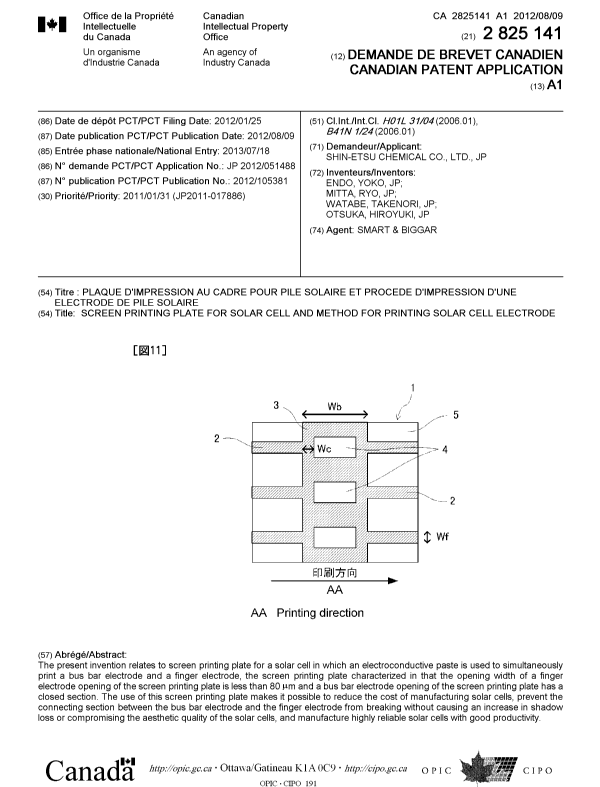
[0024]
35 FIG. 1 is a cross-sectional view of electrodes of a
typical solar cell.
-8-
CA 02825141 2013-07-18
FIG. 2 is a plan view showing the front surface
configuration of a typical solar cell.
FIG. 3 is a plan view showing the back surface
configuration of a typical solar cell.
FIG. 4 schematically illustrates a printing step using
a conventional screen printing plate.
FIG. 5 schematically illustrates a saddle phenomenon
during the printing step using a conventional screen printing
plate.
FIG. 6 is a cross-sectional view showing the profile
of an electrode as printed using the conventional screen
printing plate.
FIG. 7 schematically illustrates one exemplary method
of avoiding breakage using a conventional screen printing
plate.
FIG. 8 is an enlarged view of openings in a
conventional screen printing plate.
FIG. 9 is an enlarged view of electrodes printed using
the conventional screen printing plate.
FIG. 10 is a cross-sectional view of the connections
between bus bar electrode and finger electrode taken along
line A-A in FIG. 9.
FIG. 11 is an enlarged view showing openings on a
screen printing plate in one embodiment of the invention.
FIG. 12 is an enlarged view of electrodes printed using
the screen printing plate in one embodiment of the invention.
FIG. 13 is a cross-sectional view of the connections
between bus bar electrode and finger electrode taken along
line B-B in FIG. 12.
DESCRIPTION OF EMBODIMENTS
[0025]
One embodiment of the invention is described below in
detail. The screen printing plate for use in the manufacture
of solar cells includes a bus bar electrode-providing portion
including a blocked zone. In a preferred embodiment, the
blocked zone accounts for up to 60%, more preferably up to
-9-
CA 02825141 2013-07-18
55% of an opening area computed from the contour of the bus
bar electrode. The invention exerts its effect more when the
blocked zone accounts for at least 30%, more preferably at
least 45% of the opening area. The screen printing plate
also includes a finger electrode opening having a width of
less than 80 gm, preferably 40 pm to less than 80 gm, more
preferably 40 to 75 pm, even more preferably 45 to 70 gm, and
most preferably 50 to 60 pm.
[0026]
FIG. 11 illustrates an exemplary screen printing plate
of the invention. In FIG. 11, the screen printing plate 1
includes a plurality of finger electrode openings 2 extending
parallel to the printing direction (shown by arrow) and a bus
bar electrode opening 3 of a broad width (Wb) extending
perpendicular to the printing direction. The width Wb is
preferably 0.5 to 3 mm, more preferably 1 to 2 mm. In the
screen printing plate 1 according to the invention, the bus
bar electrode opening 3 includes a plurality of blocked zones
4 arranged therein. These blocked zones 4 are formed at
positions aligned with the longitudinal direction of the
finger electrode openings 2. The blocked zone 4 within the
bus bar electrode opening 2 is preferably spaced apart a
distance (Wc) of 50 to 700 gm, more preferably 100 to 300 pm
from the boundary between finger electrode opening 2 and bus
bar electrode opening 3. If the distance is less than 50 pm,
then the amount of paste discharged may be reduced, inviting
breakage. If the distance exceeds 700 pm, then the push-out
of paste by pressing of the squeegee becomes outstanding for
a saddle phenomenon to occur, leaving a risk of breakage due
to differential shrinkage upon firing. The spacing between
blocked zones 4 is preferably 100 to 2,000 gm, more
preferably 300 to 1,000 gm.
[0027]
The total area of blocked zones 4 is up to 60% of the
overall area of the bus bar electrode opening 3 and blocked
-10-
CA 02825141 2013-07-18
zones 4 (that is, bus bar area computed from the contour of
bus bar electrode opening 3 of the screen printing plate).
The width Wf of the finger electrode opening 2 is less than
80 gm.
Use of the screen printing plate configured as above
is effective for preventing breakage of the finger electrodes,
fall-down of the squeegee in the bus bar electrode opening
during printing, and a thickening of the finger electrode at
transition from the bus bar electrode to the finger electrode,
lo as best shown in FIGS. 12 and 13.
[0028]
Now, one exemplary method of fabricating a solar cell
using the screen printing plate according to the invention is
described. The invention is not limited to the solar cell
fabricated by this method.
An as-cut monocrystalline (100) p-type silicon
substrate in which high purity silicon is doped with a Group
III element such as boron or gallium so as to give a
resistivity of 0.1 to 5 12-cm is etched with a conc. alkali
solution of sodium hydroxide or potassium hydroxide having a
concentration of 5 to 60% by weight or mixed acid of
hydrofluoric acid and nitric acid for removing the work
damaged surface layer. The monocrystalline silicon substrate
may have been prepared by either the CZ or FZ method.
[0029]
Subsequently, the substrate surface is provided with
microscopic asperities known as texture. The texture is an
effective means for lowering the reflectivity of solar cells.
The texture may be readily provided by immersing the
substrate in a hot alkaline solution of sodium hydroxide,
potassium hydroxide, potassium carbonate, sodium carbonate or
sodium hydrogencarbonate (concentration 1 to 10 wt%) at a
temperature of 60 to 100 C for about 10 to about 30 minutes.
Often, a proper amount of 2-propanol is dissolved in the
alkaline solution to promote the reaction.
CA 02825141 2013-07-18
[0030]
The texturing is followed by washing with an aqueous
acidic solution such as hydrochloric acid, sulfuric acid,
nitric acid or hydrofluoric acid or a mixture thereof.
Washing with hydrochloric acid is preferred from the cost and
efficiency standpoints. To enhance cleanness, washing may be
carried out by mixing 0.5 to 5 wt% of aqueous hydrogen
peroxide with aqueous hydrochloric acid and heating at 60 to
90 C.
[0031]
On the substrate, an emitter layer is formed by vapor
phase diffusion using phosphorus oxychloride. In common
silicon solar cells, a p-n junction must be formed only on
the light-receiving surface. To this end, suitable means
must be taken for avoiding any p-n junction on the back
surface, for example, by carrying out diffusion while two
substrates are mated together, or by forming a SiO, or SiNx
film on the back surface as diffusion mask prior to diffusion.
At the end of diffusion, the glass formed on the surface is
removed using hydrofluoric acid or the like.
[0032]
Next, an antireflection film is formed on the
light-receiving surface. Using a plasma-enhanced chemical
vapor deposition (CVD) system for film formation, a SiNx film
is deposited to a thickness of about 100 nm. Often a mixture
of monosilane (Silij and ammonia (NH3) is used as the reactant
gas although nitrogen may be used instead of NH3. Also
hydrogen may be mixed with the reactant gas to adjust the
process pressure, to dilute the reactant gas, or to enhance
the bulk passivation effect when the substrate used is of
polycrystalline silicon.
[0033]
Next, a back electrode is formed by the screen
printing method. On the back surface of the substrate, a
paste obtained by mixing silver powder and glass frit with an
organic binder is screen printed in a bus bar pattern, after
which a paste obtained by mixing aluminum powder with an
-12-
CA 02825141 2013-07-18
organic binder is screen printed in the region excluding the
bus bar. After printing, the pastes are fired at a
temperature of 700 to 800 C for 5 to 30 minutes to form a
back electrode. The back electrode is preferably formed by
s the printing method, although it can be formed by evaporation,
sputtering or the like.
[0034]
Next, a front electrode is formed by the screen
printing method using the screen printing plate according to
lo the invention.
Specifically, a paste obtained by mixing silver powder
and glass frit with an organic binder is printed onto the
front surface of the substrate using a screen printing plate
having a comb-shaped printing pattern designed to a finger
ls electrode width of 30 to 80 m and a finger electrode spacing
of 0.5 to 4.0 mm.
[0035]
The screen printing plate of the invention may be
obtained simply by providing the bus bar electrode opening
20 with blocked zones as shown in FIG. 11, without a need to
change the conventional solar cell pattern as mentioned above.
[0036]
Commonly used screen printing plates include finger
openings having a width of 80 to 100 m. In this case,
25 breakage as mentioned above rarely occurs because the finger
electrodes are fully wide and can be printed thick. However,
as lines are narrowed to a finger opening width of less than
80 m, the difference in film thickness between bus bar
electrode and finger electrode becomes greater. Then breakage
30 can occur due to differential thermal shrinkage (FIG. 9).
[0037]
In contrast, when a solar cell is manufactured by
printing a bus bar electrode and a finger electrode
simultaneously, the risk of breakage is avoidable by the
35 printing step using a screen printing plate including a bus
bar electrode opening including blocked zones accounting for
-13-
CA 02825141 2013-07-18
up to 60% of the opening area computed from the contour of
the bus bar electrode (FIG. 13).
In order to take full advantage of the invention when
solar cells are manufactured by printing electrodes through
s the screen printing plate having the features described above,
it is desired that the printing direction be substantially
perpendicular to the bus bar electrode.
[0038]
The use of the screen printing plate according to the
lo invention has the additional effect of suppressing the finger
electrode from thickening because the presence of blocked
zones in the bus bar electrode opening reduces the amount of
paste discharged at the last printing side (FIG. 12).
[0039]
15 When a blocked zone is partially included in the bus
bar opening, an unprinted area may be left after the printing.
However, this causes no problems to the outer appearance
because a solder-coated copper lead is bonded to the area
upon fabrication of a module. As long as the area of bus bar
20 electrode is at least 40% of the standard bus bar electrode
area, the bond strength of the lead to the bus bar electrode
is maintained. Since the amount of bus bar electrode used is
reduced, solar cells can be manufactured at lower cost. The
inclusion of blocked zones in the bus bar electrode opening
25 of the screen printing plate avoids any breakage of the
connection between bus bar electrode and finger electrode.
Once electrodes are formed by the above-mentioned
method, they are fired by heating in air at a temperature of
700 to 800 C for 5 to 30 minutes. Firing of the back
30 electrode and light-receiving side electrode may be performed
at a time.
EXAMPLES
[0040]
35 Examples and Comparative Examples are given below by
way of illustration and not by way of limitation.
-14-
CA 02825141 2013-07-18
[0041]
[Examples and Comparative Examples]
To demonstrate the benefits of the invention, solar
cells were manufactured by processing thirty (30)
semiconductor substrates as follows.
There were provided screen printing plates bearing a
conventional pattern A having a finger electrode opening
width (Wf) of 60 m (Comparative Example, FIG. 8), a pattern
B including a bus bar electrode opening including blocked
zones (FIG. 11), otherwise equivalent to pattern A, and a
pattern C having a finger electrode opening width (Wf) of 100
m (Comparative Example, FIG. 8) as the printing pattern.
All the patterns commonly had a bus bar electrode opening
width (Wb) of 1.5 mm.
More particularly, in pattern B, the bus bar electrode
opening was spaced apart a distance Wc of 100 m from the
boundary between the finger electrode opening and the bus bar
electrode opening, the spacing between blocked zones was
1,000 m, and the total area of blocked zones was 55% of the
bus bar area computed from the contour of the bus bar
electrode opening.
[0042]
There was provided an as-cut boron-doped {100} p-type
silicon substrate 100 of 15 cm square having a thickness of
250 pm and a resistivity of 2.0 K/-cm. The substrate was
immersed in a conc. potassium hydroxide aqueous solution to
remove the work damaged layer, textured, heat treated at
850 C in a phosphorus oxychloride atmosphere to form an
emitter layer 101, and etched with hydrofluoric acid to
remove phosphorus glass, followed by washing and drying.
Thereafter, a SiNx film 102 was formed using a
plasma-enhanced CVD system. On the back surface, a paste of
silver powder, glass frit and organic binder was screen
printed in a bus bar pattern 106, after which a paste of
aluminum powder and organic binder was screen printed in a
pattern 104 excluding the bus bar. The organic solvent was
-15-
CA 02825141 2013-07-18
evaporated off, yielding a semiconductor substrate having a
back electrode formed thereon.
[0043]
Next, a conductive paste based on silver powder, glass
s frit, organic vehicle and organic solvent and further
containing a metal oxide as additive was applied onto the
antireflection film on the semiconductor substrate by using a
screen printing plate having the selected printing pattern at
a squeegee hardness of 70 degrees, a squeegee angle of 70
lo degrees, an applied pressure of 0.3 MPa, and a printing speed
of 50 mm/sec. After printing, the substrate was heated in a
clean oven at 150 C for drying and fired in air at 800 C.
[0044]
Thirty (30) solar cells thus manufactured were
15 observed for electrodes under an optical microscope and
evaluated by a solar simulator (25 C atmosphere, irradiation
intensity 1 kW/m2, spectrum AM 1.5 Global). Also under the
optical microscope, the width of finger electrodes after
printing and the width of connection were observed to inspect
20 any breakage. The results on average of Example and
Comparative Examples are shown in Table 1.
[0045]
Table 1
Short-
Finger Bus bar Fill Conversion
Blocked circuit
Level opening opening zones current Breakage
factor efficiency
(pm) (mm)
(mA/ce) (%) (%)
A (Comparative
60 1.5 absent found 35.1 73.6 15.50
Example)
B (Example) 60 1.5 present none 35.1 75.1 15.82
C (Comparative
100 1.5 absent none 33.8 76.2 15.20
Example)
-16-
CA 02825141 2013-07-18
[0046]
Breakage at the connection between bus bar electrode
and finger electrode was observed under standard level A, but
not in the method of the invention and also under level C
s using a large opening width.
The short-circuit current dropped under level C using
a large finger electrode width. This drop is caused by a
shadow loss due to the increased width. The fill factor
under level B free of breakage was 75.1%, which was about
lo 1.5% higher than that under level A undergoing breakage.
In the prior art, breakage at the connection between
bus bar electrode and finger electrode occurred. Using the
screen printing plate of the invention, electrodes having a
high aspect ratio can be formed at no risk of breakage
15 without increasing the number of steps.
[0047]
As demonstrated above, the invention ensures that bus
bar electrode and finger electrode are formed at no risk of
breakage at the connection between bus bar electrode and
20 finger electrode. Thus solar cells having a high conversion
efficiency can be manufactured in high yields.
Reference Signs List
[0048]
25 1 screen printing plate
2 finger electrode opening
3 bus bar electrode opening
4 blocked zone in bus bar electrode opening
blocked zone
30 12 finger electrode
13 front bus bar electrode
100 p-type semiconductor substrate
101 n-type diffusion layer
102 antireflection film (SiNx film)
35 103 BSF layer
104 aluminum electrode
105 front bus bar electrode
-17-
CA 02825141 2013-07-18
106 back bus bar electrode
107 finger electrode
110 mesh fabric
111 emulsion
112 squeegee
113 dent
114 breakage
-18-