Note: Descriptions are shown in the official language in which they were submitted.
CA 02825191 2013 07 18
WO 2012/099863 PCT/US2012/021524
A METHOD FOR ATTACHING AN ELECTRONIC ASSEMBLY TO A BOTTOM
OVERLAY IN THE MANUFACTURE OF AN ELECTRONIC DEVICE
BACKGROUND
[0001] The present invention relates generally to the field of devices
containing
electronic assemblies.
[0002] Generally, these devices may be used as credit cards, bankcards, ID
cards,
telephone cards, security cards, smart cards, lifestyle cards, tags or similar
devices.
These devices are generally constructed by assembling several layers of
plastic sheets
in a sandwich array. Further, these devices may contain electronic assemblies
that
enable the device to perform a number of functions.
[0003] European Patent 0 350 179 discloses a smart card wherein electronic
circuitry is
encapsulated in a layer of plastic material that is introduced between the
card's two
surface layers. The method disclosed further comprises abutting a high tensile
strength holding member against a side of a mold, locating the smart card's
electronic
components with respect to that side and then injecting a reaction moldable
polymeric
material into the mold such that it encapsulates the electronic components.
[0004] European Patent Application 95400365.3 teaches a method for making
contact-
less smart cards. The method employs a rigid frame to position and fix an
electronic
module in a void space between an upper thermoplastic sheet and a lower
thermoplastic
sheet. After the frame is mechanically affixed to the lower thermoplastic
sheet, the
void space is filled with a polymerizable resin material.
[0005] U.S. Patent No. 5,399,847 teaches a credit card that is comprised of
three
layers, namely, a first outer layer, a second outer layer and an intermediate
layer. The
intermediate layer is formed by injection of a thermoplastic binding material
that
encases the smart card's electronic elements (e.g., an 1C chip and an antenna)
in the
intermediate layer material. The binding material is preferably made up of a
blend of
copolyamides or a glue having two or more chemically reactive components that
CA 02825191 2013 07 18
WO 2012/099863 PCT/US2012/021524
harden upon contact with air. The outer layers of this smart card can be made
up of
various polymeric materials, such as polyvinyl chloride or polyurethane.
[0007] U.S. Patent No. 5,417,905 teaches a method for manufacturing plastic
credit
cards wherein a mold tool comprised of two shells is closed to define a cavity
for
producing such cards. A label or image support is placed in each mold shell.
The
mold shells are then brought together and a thermoplastic material is injected
into the
mold to form the card. The inflowing plastic forces the labels or image
supports
against the respective mold faces.
[0008] U.S. Patent No. 5,510,074 teaches a method of manufacturing smart cards
having a card body with substantially parallel major sides, a support member
with a
graphic element on at least one side, and an electronic module comprising a
contact
array that is fixed to a chip. The manufacturing method generally comprises
the steps of:
(1) placing the support member in a mold that defines the volume and shape of
the card;
(2) holding the support member against a first main wall of the mold; (3)
injecting a
thermoplastic material into the volume defined by the hollow space hi order to
fill that
portion of the volume that is not occupied by the support member; and (4)
inserting an
electronic module at an appropriate position in the thermoplastic material
before the
injected material has the opportunity to completely solidify.
[0009] U.S. Patent No. 4,339,407 discloses an electronic circuit encapsulation
device in
the form of a carrier having walls that have a specific arrangement of lands,
grooves
and bosses in combination with specific orifices. The mold's wall sections
hold a circuit
assembly in a given alignment. The walls of the carrier are made of a slightly
flexible
material in order to facilitate insertion of the smart card's electronic
circuitry. The carrier
is capable of being inserted into an outer mold. This causes the carrier walls
to move
toward one another in order to hold the components securely in alignment
during the
injection of the thermoplastic material. The outside of the walls of the
carrier has
projections that serve to mate with detents on the walls of the mold in order
to locate
and fix the carrier within the mold. The mold also has holes to permit the
escape of
trapped gases.
2
CA 02825191 2013 07 18
WO 2012/099863 PCT/US2012/021524
[0010] U.S. Patent No. 5,350,553 teaches a method of producing a decorative
pattern on,
and placing an electronic circuit in, a plastic card in an injection molding
machine. The
method comprises the steps of: (a) introducing and positioning a film (e.g., a
film bearing
a decorative pattern) over an open mold cavity in the injection molding
machine; (b)
closing the mold cavity so that the film is fixed and clamped in position
therein; (c)
inserting an electronic circuit chip through an aperture in the mold into the
mold cavity hi
order to position the chip in the cavity; (d) injecting a thermoplastic
support
composition into the mold cavity to form a unified card; (e) removing any
excess
material; (f) opening the mold cavity; and (g) removing the card.
[0011] U.S. Patent No. 4,961,893 teaches a smart card whose main feature is a
support element that supports an integrated circuit chip. The support element
is used for
positioning-the chip inside a mold cavity. The card body is formed by
injecting a plastic
material into the cavity so that the chip is entirely embedded in the plastic
material. In
some embodiments, the edge regions of the support are clamped between the load
bearing
surfaces of the respective molds. The support element may be a film that is
peeled off the
finished card or it may be a sheet that remains as an integral part of the
card. If the
support element is a peel-off film, then any graphics elements contained
therein are
transferred and remain visible on the card. If the support element remains as
an
integral part of the card, then such graphics elements are formed on a face
thereof and,
hence, are visible to the card user.
[0012] U.S. Patent No. 5,498,388 teaches a smart card device that includes a
card board
having a through-opening. A semiconductor module is mounted onto this opening.
A
resin is injected into the opening so that a resin molding is formed under
such condition
that only an electrode terminal face for external connection of said
semiconductor
module is exposed. The card is completed by mounting a card board having a
through-
opening onto a lower mold of two opposing molding dies, mounting a
semiconductor
module onto the opening of said card board, tightening an upper die that has a
gate
leading onto a lower die and injecting a resin into the opening via the gate.
[0013] U.S. Patent No. 5,423,705 teaches a disc having a disc body made of a
3
CA 02825191 2013 07 18
WO 2012/099863 PCT/US2012/021524
thermoplastic injection molded material and a laminate layer that is
integrally joined to a
disc body. The laminate layer includes an outer clear lamina and an inner
white and
opaque lamina. An imaging material is sandwiched between these lamina.
[0014] U.S. Patent No. 6,025,054 discloses a method for constructing a smart
card
using low shrinkage glue to hold the electronic devices in place during the
devices
immersion in thermosetting material that becomes the core layer of the smart
card.
[0015] Generally, all of the above methods involve using specialized
processes,
pedestals, anchors or other devices for adhering the electronic assemblies to
one of the
printed overlays.
SUMMARY
[0016] According to one embodiment, a method is disclosed that includes the
steps of
using a unique modified UV curable adhesive to affix to the top surface of a
bottom
overlay to a circuit board with an electronic assembly, loading the electronic
assembly
adhered to the bottom overlay into an injection molding apparatus, loading a
top overlay
positioned above a top surface of the electronic assembly into the injection
molding
apparatus, closing the molding apparatus, and injecting a thermosetting
polymeric
material between the top and bottom overlays.
[0017] It is to be understood that the foregoing general description and the
following
detailed descriptions are exemplary and explanatory only, and are not
restrictive of the
invention as claimed.
BRIEF DESCRIPTION OF THE DRAWINGS
[0018] These and other features, aspects and advantages of the present
invention will
become apparent from the following description, appended claims, and the
accompanying exemplary embodiments shown in the drawings, which are briefly
described below.
4
CA 02825191 2013 07 18
WO 2012/099863
PCT/US2012/021524
[0019] FIG. 1 shows a schematic view of the top side of an overlay that has
had the
circuit outline screen printed with unique modified UV curable adhesive.
[0020] FIG. 2 shows a schematic view of the top side of an overlay with a
circuit
placed on top of the screen printed unique modified UV curable adhesive.
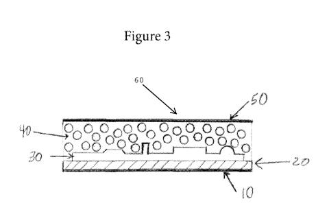
[0021] FIG. 3 shows a cross sectional view of an electronic device consisting
of a
bottom overlay, a layer of unique modified UV curable adhesive screen printed
to the
top side of the bottom overlay, an electronic assembly attached to the top
side of the
printed unique modified UV curable adhesive, and a layer of injected
thermosetting
material between the bottom side of a top overlay and the top side of the
electronic
assembly.
[0022] FIG. 4 is a flowchart illustrating a process for forming an electronic
device.
DETAILED DESCRIPTION
[0023] FIG. 1 shows a schematic view of the top side of a bottom overlay 10
for an
electronic device 60. As shown in FIG. 1 and in steps 100 and 110 of Fig. 4, a
unique
modified UV curable adhesive 20 is affixed to the top side of a bottom overlay
10
exhibiting an area just slightly larger than the perimeter measurement of an
electronic
assembly. The UV curable adhesive 20 is configured to be applied to a surface
in
controlled amounts. The UV curable adhesive 20 can be affixed via screen
printing,
spray or any other known application for applying adhesive 20 to a surface.
[0024] Next, in step 120, the bottom overlay 10, having the applied unique
modified
UV curable adhesive 20, is processed through an ultra violet light system to
activate
the unique modified UV curable adhesive 20. Upon application of UV light, the
UV
curable adhesive 20 becomes tacky or sticky.
[0025] As shown in FIG. 2, in step 130 an electronic assembly 30 is placed on
the top
side of the screen printed unique modified UV curable adhesive 20. The
electronic
assembly 30 may include one or more circuit components, including but not
limited to a
printed circuit board, a button, a switch, a battery, an LCD or other
electronic
components that may be required or useful in an electronic device 60. Because
the UV
CA 02825191 2013 07 18
WO 2012/099863
PCT/US2012/021524
curable adhesive 20 has been exposed to UV light and is sticky or tacky, the
electronic
assembly 30 can be easily affixed to the UV curable adhesive 20. The UV
curable
adhesive 20 then cures for a period of time to create a permanent bond.
Preferably, it
takes approximately twenty-four hours for the UV curable adhesive 20 to cure.
The fact
that the UV curable adhesive 20 does not cure upon immediate exposure to UV
light
makes it extremely flexible and ideal for the electronic device manufacturing
process.
[0026] Then, in step 140 the bottom overlay 10 with the electronic assembly 30
attached is loaded into a mold with the electronic assembly 30 positioned on
top. In
step 150, a top overlay 50 that has a top surface and a bottom surface is
loaded above
the electronic assembly 30 that is affixed to the top surface of the bottom
overlay 10.
Next, in step 160, the mold is closed and a thermosetting polymeric material
40 is
injected between the top overlay 50 and bottom overlay 10. In step 170, the
mold is
opened and the injected top overlay 50 and bottom overlay 10 containing the
electronic assembly 30 is removed from the mold. Finally, the electronic
device 60 is
cut out based size specifications, etc. FIG. 3 shows a completed electronic
device 60,
having a bottom overlay 10, a unique modified UV curable adhesive 20 affixed
on the
top side of the bottom overlay 10, an electronic assembly 30 adhered to the
top side of
the screen printed unique modified UV curable adhesive 20, and a layer of
thermoset
material 40 positioned between the top of the electronic assembly 30 and the
bottom
side of the top overlay 50.
[0027] Given the disclosure of the present invention, one versed in the art
would
appreciate that there may be other embodiments and modifications within the
scope
and spirit of the invention. Accordingly, all modifications attainable by one
versed in
the art from the present disclosure within the scope and spirit of the present
invention
are to be included as further embodiments of the present intention. The scope
of the
present invention is to be defined as set forth in the following claims.
6