Some of the information on this Web page has been provided by external sources. The Government of Canada is not responsible for the accuracy, reliability or currency of the information supplied by external sources. Users wishing to rely upon this information should consult directly with the source of the information. Content provided by external sources is not subject to official languages, privacy and accessibility requirements.
Any discrepancies in the text and image of the Claims and Abstract are due to differing posting times. Text of the Claims and Abstract are posted:
| (12) Patent: | (11) CA 2825529 |
|---|---|
| (54) English Title: | RADAR-TRANSPARENT COATING |
| (54) French Title: | REVETEMENT TRANSPARENT AUX ONDES RADAR |
| Status: | Granted and Issued |
| (51) International Patent Classification (IPC): |
|
|---|---|
| (72) Inventors : |
|
| (73) Owners : |
|
| (71) Applicants : |
|
| (74) Agent: | SMART & BIGGAR LP |
| (74) Associate agent: | |
| (45) Issued: | 2019-10-22 |
| (86) PCT Filing Date: | 2011-12-23 |
| (87) Open to Public Inspection: | 2012-08-02 |
| Examination requested: | 2016-09-26 |
| Availability of licence: | N/A |
| Dedicated to the Public: | N/A |
| (25) Language of filing: | English |
| Patent Cooperation Treaty (PCT): | Yes |
|---|---|
| (86) PCT Filing Number: | PCT/EP2011/006545 |
| (87) International Publication Number: | WO 2012100805 |
| (85) National Entry: | 2013-07-24 |
| (30) Application Priority Data: | |||||||||
|---|---|---|---|---|---|---|---|---|---|
|
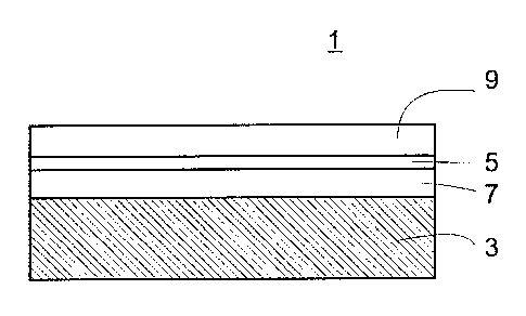
The invention relates to a radar-transparent component comprising a plastic
body. Said
component is characterized in that at least parts of the surface have a
coating with a
thickness of between 10nm and 100nm that comprises a semiconductor. Said
coating gives
the plastic body the desired metallic appearance without the body losing the
characteristic
of a radar-transparent component.
La présente invention concerne un élément transparent aux ondes radar comprenant un corps en matière plastique. Ledit élément est caractérisé en ce qu'au moins des parties de la surface présentent une couche comprenant un semi-conducteur et dont l'épaisseur est comprise entre 10 nm et 100 nm. Ce revêtement permet de conférer au corps en matière plastique une apparence métallique souhaitée, sans altérer sa propriété d'élément transparent aux ondes radar.
Note: Claims are shown in the official language in which they were submitted.
Note: Descriptions are shown in the official language in which they were submitted.
2024-08-01:As part of the Next Generation Patents (NGP) transition, the Canadian Patents Database (CPD) now contains a more detailed Event History, which replicates the Event Log of our new back-office solution.
Please note that "Inactive:" events refers to events no longer in use in our new back-office solution.
For a clearer understanding of the status of the application/patent presented on this page, the site Disclaimer , as well as the definitions for Patent , Event History , Maintenance Fee and Payment History should be consulted.
| Description | Date |
|---|---|
| Common Representative Appointed | 2019-10-30 |
| Common Representative Appointed | 2019-10-30 |
| Grant by Issuance | 2019-10-22 |
| Inactive: Cover page published | 2019-10-21 |
| Inactive: Final fee received | 2019-08-23 |
| Pre-grant | 2019-08-23 |
| Notice of Allowance is Issued | 2019-06-27 |
| Letter Sent | 2019-06-27 |
| Notice of Allowance is Issued | 2019-06-27 |
| Inactive: Q2 passed | 2019-06-14 |
| Inactive: Approved for allowance (AFA) | 2019-06-14 |
| Amendment Received - Voluntary Amendment | 2019-01-24 |
| Inactive: S.30(2) Rules - Examiner requisition | 2018-07-24 |
| Inactive: Report - No QC | 2018-07-20 |
| Amendment Received - Voluntary Amendment | 2018-01-12 |
| Maintenance Request Received | 2017-12-14 |
| Inactive: S.30(2) Rules - Examiner requisition | 2017-07-12 |
| Inactive: Report - No QC | 2017-07-11 |
| Letter Sent | 2016-10-04 |
| Letter Sent | 2016-09-30 |
| Inactive: Single transfer | 2016-09-29 |
| Request for Examination Requirements Determined Compliant | 2016-09-26 |
| All Requirements for Examination Determined Compliant | 2016-09-26 |
| Request for Examination Received | 2016-09-26 |
| Letter Sent | 2015-04-15 |
| Change of Address or Method of Correspondence Request Received | 2015-01-15 |
| Maintenance Request Received | 2013-12-11 |
| Inactive: Cover page published | 2013-10-04 |
| Inactive: First IPC assigned | 2013-09-10 |
| Inactive: Notice - National entry - No RFE | 2013-09-10 |
| Inactive: Applicant deleted | 2013-09-10 |
| Inactive: IPC assigned | 2013-09-10 |
| Inactive: IPC assigned | 2013-09-10 |
| Inactive: IPC assigned | 2013-09-10 |
| Application Received - PCT | 2013-09-10 |
| National Entry Requirements Determined Compliant | 2013-07-24 |
| Application Published (Open to Public Inspection) | 2012-08-02 |
There is no abandonment history.
The last payment was received on 2018-11-19
Note : If the full payment has not been received on or before the date indicated, a further fee may be required which may be one of the following
Please refer to the CIPO Patent Fees web page to see all current fee amounts.
| Fee Type | Anniversary Year | Due Date | Paid Date |
|---|---|---|---|
| Basic national fee - standard | 2013-07-24 | ||
| MF (application, 2nd anniv.) - standard | 02 | 2013-12-23 | 2013-12-11 |
| MF (application, 3rd anniv.) - standard | 03 | 2014-12-23 | 2014-09-29 |
| Registration of a document | 2015-02-27 | ||
| MF (application, 4th anniv.) - standard | 04 | 2015-12-23 | 2015-08-31 |
| MF (application, 5th anniv.) - standard | 05 | 2016-12-23 | 2016-08-24 |
| Request for examination - standard | 2016-09-26 | ||
| Registration of a document | 2016-09-29 | ||
| MF (application, 6th anniv.) - standard | 06 | 2017-12-27 | 2017-12-14 |
| MF (application, 7th anniv.) - standard | 07 | 2018-12-24 | 2018-11-19 |
| Final fee - standard | 2019-08-23 | ||
| MF (patent, 8th anniv.) - standard | 2019-12-23 | 2019-12-13 | |
| MF (patent, 9th anniv.) - standard | 2020-12-23 | 2020-12-22 | |
| MF (patent, 10th anniv.) - standard | 2021-12-23 | 2021-12-14 | |
| MF (patent, 11th anniv.) - standard | 2022-12-23 | 2022-12-20 | |
| MF (patent, 12th anniv.) - standard | 2023-12-27 | 2023-10-26 |
Note: Records showing the ownership history in alphabetical order.
| Current Owners on Record |
|---|
| OERLIKON SURFACE SOLUTIONS AG, PFAFFIKON |
| Past Owners on Record |
|---|
| ANTAL KECKES |
| CARLOS RIBEIRO |
| PETER SCHULER |

