Sélection de la langue

Search

Sommaire du brevet 2825529 

Énoncé de désistement de responsabilité concernant l'information provenant de tiers

Une partie des informations de ce site Web a été fournie par des sources externes. Le gouvernement du Canada n'assume aucune responsabilité concernant la précision, l'actualité ou la fiabilité des informations fournies par les sources externes. Les utilisateurs qui désirent employer cette information devraient consulter directement la source des informations. Le contenu fourni par les sources externes n'est pas assujetti aux exigences sur les langues officielles, la protection des renseignements personnels et l'accessibilité.

Disponibilité de l'Abrégé et des Revendications

L'apparition de différences dans le texte et l'image des Revendications et de l'Abrégé dépend du moment auquel le document est publié. Les textes des Revendications et de l'Abrégé sont affichés :

  • lorsque la demande peut être examinée par le public;
  • lorsque le brevet est émis (délivrance).
(12) Brevet: (11) CA 2825529
(54) Titre français: REVETEMENT TRANSPARENT AUX ONDES RADAR
(54) Titre anglais: RADAR-TRANSPARENT COATING
Statut: Octroyé
Données bibliographiques
(51) Classification internationale des brevets (CIB):
  • H01Q 1/42 (2006.01)
  • H01Q 1/32 (2006.01)
  • H01Q 1/44 (2006.01)
(72) Inventeurs :
  • KECKES, ANTAL (Allemagne)
  • SCHULER, PETER (Allemagne)
  • RIBEIRO, CARLOS (Viet Nam)
(73) Titulaires :
  • OERLIKON SURFACE SOLUTIONS AG, PFAFFIKON (Suisse)
(71) Demandeurs :
  • OERLIKON TRADING AG, TRUBBACH (Suisse)
(74) Agent: SMART & BIGGAR LP
(74) Co-agent:
(45) Délivré: 2019-10-22
(86) Date de dépôt PCT: 2011-12-23
(87) Mise à la disponibilité du public: 2012-08-02
Requête d'examen: 2016-09-26
Licence disponible: S.O.
(25) Langue des documents déposés: Anglais

Traité de coopération en matière de brevets (PCT): Oui
(86) Numéro de la demande PCT: PCT/EP2011/006545
(87) Numéro de publication internationale PCT: WO2012/100805
(85) Entrée nationale: 2013-07-24

(30) Données de priorité de la demande:
Numéro de la demande Pays / territoire Date
61/436,665 Etats-Unis d'Amérique 2011-01-27
10 2011 016 683.1 Allemagne 2011-04-11

Abrégés

Abrégé français

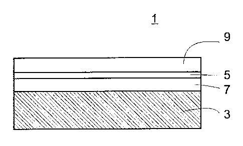
La présente invention concerne un élément transparent aux ondes radar comprenant un corps en matière plastique. Ledit élément est caractérisé en ce qu'au moins des parties de la surface présentent une couche comprenant un semi-conducteur et dont l'épaisseur est comprise entre 10 nm et 100 nm. Ce revêtement permet de conférer au corps en matière plastique une apparence métallique souhaitée, sans altérer sa propriété d'élément transparent aux ondes radar.


Abrégé anglais


The invention relates to a radar-transparent component comprising a plastic
body. Said
component is characterized in that at least parts of the surface have a
coating with a
thickness of between 10nm and 100nm that comprises a semiconductor. Said
coating gives
the plastic body the desired metallic appearance without the body losing the
characteristic
of a radar-transparent component.

Revendications

Note : Les revendications sont présentées dans la langue officielle dans laquelle elles ont été soumises.


6
CLAIMS:
1. Radar-transparent component comprising:
a radar-transparent body and
a coating on at least part of the surface of the radar-transparent body, the
coating having a thickness between 10 nm and 100 nm and comprising at least
one
semiconductor material
wherein the coating comprising at least one semiconductor material is a
component of a layer system comprising at least one further layer.
2. Radar-transparent component according to claim 1, wherein the coating
comprising at least one semiconductor material comprises silicon.
3. Radar-transparent component according to claim 1, wherein the at least
one
further layer is SiO2.
4. Radar-transparent component according to claim 1, wherein the layer
system is an alternating layer system.
5. Radar-transparent component according to claim 1, wherein between the
radar-transparent body and the coating comprising at least one semiconductor,
an
intermediary layer is provided comprising a polymer layer.
6. Radar-transparent component according to claim 1, wherein as a sealing
layer against the environment, a polymer coating is provided.
7. Radar-transparent component according to claim 1, wherein the radar-
transparent body is a plastic body.
8. Radar-transparent component according to claim 2, wherein the coating
comprises silicon as a main component.

7
9. Radar-transparent component according to claim 2, wherein the coating
consists of silicon.
10. Radar-transparent component according to claim 1, wherein the layer
system comprises an interference layer system.
11. Radar-transparent component according to claim 5, wherein the polymer
layer consists of a UV-hardened lacquer.
12. Radar-transparent component according to claim 6, wherein the polymer
coating consists of a UV-hardened lacquer.
13. Cladding element with a radar-transparent component according to any
one
of claim 1 to 12, wherein this cladding element is a cladding element for a
motor
vehicle.
'14. Method for producing a radar-transparent component, having the steps
of:
providing a radar-transparent body and
coating the radar-transparent body with a coating comprising a
semiconductor material and at least one further layer to form a component of a
layer
system,
wherein the coating thickness is between 10 nm and 100 nm, and
wherein the coating is achieved by means of a vacuum process.
15. Method according to claim 14, wherein the vacuum process is a PVD
and/or
a CVD process.
16. Method according to claim 14 or 15, wherein the radar-transparent body
is a
plastic body.

Description

Note : Les descriptions sont présentées dans la langue officielle dans laquelle elles ont été soumises.


CA 02825529 2013-07-24
1
RADAR-TRANSPARENT COATING
The present invention relates to a radar device placed behind a cladding,
wherein at least
parts of the cladding lie in the ray path of the radar device. A radar device
can mean for
example a radar ray source, a sensor for radar waves or the combination of
both.
Radar devices are used for example in vehicles for measuring the distance.
Often, such a
device is placed behind the front grille of the vehicle. The corresponding
radar device
should not be visible from the outside and must therefore be placed behind a
cladding. The
radar waves relevant for these applications are preferably in the frequency
range around
76-77 GHz. The cladding should be to a large extent penetrable to radar waves
in this
frequency range, however on the other hand produce the desired optical
impression. A
metallic appearance in particular is often desired.
DE 198 44 021 discloses a cladding part of plastic lying within the ray path
of a radar
device with a portion of metal visible from the outside, wherein the portion
of metal is
formed of an extremely thin, i.e. 40nm thick, vaporized metallic coating. This
coating,
according to the description in question, corresponds optically to the
neighboring chrome
trim strips referred to therein.
It is possible with the arrangement disclosed in DE 198 44 021 to achieve an
optically
metallic impression. However, due to the metallic properties of the coating
and despite the
low coating thickness, a non-negligible portion of the radar waves continues
to be absorbed
and is no longer available as signal. Furthermore, the use of metallic
coatings essentially
allows no adaptations in terms of the optical impression. The latter therefore
cannot be
varied at all or only to a very small extent.
It is thus an aim of the present invention to overcome or at least mitigate
the problems,
described above, of the prior art.
According to the invention, this aim is achieved in that a cladding formed of
radar-
transparent material, such as for example plastic, is coated with a thin
layer, preferably

CA 02825529 2013-07-24
2
W02012100805
between 10nm and 100nm thick, that comprises at least one semiconductor
material
(hereinafter also called semiconductor layer). For this purpose, silicon is
particularly
suitable as a coating material. This coating can be obtained by means of
physical vapor
deposition (PVD). Dense, and thus preferred, coatings can be achieved by means
of a
magnetron sputtering process. It is however also possible to use chemical
vapor deposition
(CVD).
In the frame of this description, a semiconductor layer and a layer comprising
at least a
semiconductor are to be considered equivalent.
In the frame of this description, a component is considered a radar-
transparent component
if, when radar rays pass twice through the component, at least 0.1% of the
intensity I
reaches the sensor, relatively to the intensity lo which would otherwise reach
the sensor
without passing through the component. Preferably, at least 1% (I/ lo 1%) will
arrive, even
more preferably 5% or more. Figure 4 sketches a measurement set-up, with a
radar source
403, a reflection objet 405, a radar sensor 407 and the component 409 to be
measured.
The ray path is indicated by arrows. The reference measurement of the
intensity lo is
performed without the component 405. The transmission measurement of the
intensity I is
performed with the component 405.
The invention will now be described in more detail on the basis of examples
and of the
figures.
Fig. 1 shows an inventive component 101 with a radar-transparent body 103 and
a coating
105 comprising a semiconductor material.
Fig. 2 shows a component 1 comprising a radar-transparent body 3, for example
a plastic
body, and a coating 5 comprising a semiconductor, as well as a polymer layer 7
between
the layer 5 and the substrate and a polymer layer 9 on the coating 5.
Fig. 3 shows an inventive component 201 with radar-transparent body 203,
wherein the
coating 205 comprising the semiconductor is embedded between a polymer layer
209 and
an alternating layer system 207. The alternating layer system is executed as
an
interference layer system. The one skilled in the art can use the commercially
available

=
CA 02825529 2013-07-24
3
W02012100805
thin-film design programs such as for example OptiLayer, in order to achieve
the desired
optical function. In particular, the semiconductor coating can be positioned
at will or can
also be separated into several thinner layers.
According to a first embodiment of the present invention, a silicon layer with
a thickness of
35 nm (i.e. within the lOnm to 100nm thickness range) is deposited as
semiconductor layer
onto a black plastic substrate. In order to smooth any potential surface
structures, a primer
(UV acryl lacquer) is first applied onto the plastic surface. After applying
the Si-layer by
means of magnetron sputtering, a top layer (UV acryl lacquer) is applied in
the present
example for additional protection of the thin Si-layer. This results in a
bluish to yellowish
metallically shimmering surface. The radar transparency at 76-77GHz of the
substrate
coated according to the invention is not essentially less than that of the
comparable
uncoated substrate.
A diagrammatic representation corresponding to the first embodiment is shown
in figure 2.
According to a second embodiment of the present invention, the semiconductor
layer is
executed as a layer system, preferably as an interference layer system. This
can for
example be structured as alternating layer system with a semiconductor, e.g.
Si and a
dielectric, e.g. Si02. The total thickness of the Si-layers should in this
case again be in the
range between lOnm and 100nm. In order to achieve the desired transmission and

reflection characteristic in the visible range of the spectrum of
electromagnetic rays,
performance-enhanced optimization programs for optical thin-films are nowadays
available
to the one skilled in the art. A more in-depth explanation in this respect is
therefore
eschewed in the present case.
According to a third embodiment of the present invention, Germanium is used as

semiconductor material for the coating. This coating can also be executed as
an individual
thin monolayer with a thickness of lOnm to 100nm or as an alternating layer
system with
one or several dielectrics, such as for example Si02. In particular, Ge can
also be
combined with Si in order to achieve the desired effects.

CA 02825529 2013-07-24
=
4
W02012100805
the frame of this description, a radar-transparent component was disclosed
that
comprises a radar-transparent body, preferably a plastic body, wherein at
least parts of the
surface have a coating with a thickness between lOnnn and 100nm that comprises
at least
one semiconductor material.
The coating comprising at least one semiconductor can comprise silicon,
preferably
comprises silicon as a main component and even more preferably consists
essentially of
silicon.
The layer comprising at least one semiconductor can be a component of a layer
system
comprising at least one further layer, which is preferably an interference
layer system.
The at least one other layer can be Si02.
The layer system can be an alternating layer system.
Between the plastic body and the coating comprising at least one
semiconductor, it is
possible to provide an intermediary layer comprising a polymer layer that
preferably
consists of a UV-hardened lacquer.
On the radar-transparent component, it is possible to provide as sealing layer
against the
environment a polymer coating, which preferably consists of a UV-hardened
lacquer.
The radar-transparent component can be part of a cladding element, wherein
this cladding
element is preferably a cladding element for a motor vehicle.
A vehicle with a radar device is disclosed, wherein a radar-transparent
component
according to the possibilities described above is provided in the ray path of
the radar device
and this component is preferably at least part of a cladding element.
A method for producing a radar-transparent component is disclosed, having the
steps of:
- providing a plastic body
- coating the plastic body with a coating comprising a semiconductor
material and whose
thickness is between 10nm and 100nm, wherein the coating is achieved by means
of a
vacuum process.

CA 02825529 2013-07-24
W02012100805
The vacuum process is preferably a PVD and/or a CVD process.

Dessin représentatif
Une figure unique qui représente un dessin illustrant l'invention.
États administratifs

Pour une meilleure compréhension de l'état de la demande ou brevet qui figure sur cette page, la rubrique Mise en garde , et les descriptions de Brevet , États administratifs , Taxes périodiques et Historique des paiements devraient être consultées.

États administratifs

Titre Date
Date de délivrance prévu 2019-10-22
(86) Date de dépôt PCT 2011-12-23
(87) Date de publication PCT 2012-08-02
(85) Entrée nationale 2013-07-24
Requête d'examen 2016-09-26
(45) Délivré 2019-10-22

Historique d'abandonnement

Il n'y a pas d'historique d'abandonnement

Taxes périodiques

Dernier paiement au montant de 263,14 $ a été reçu le 2023-10-26


 Montants des taxes pour le maintien en état à venir

Description Date Montant
Prochain paiement si taxe générale 2024-12-23 347,00 $
Prochain paiement si taxe applicable aux petites entités 2024-12-23 125,00 $

Avis : Si le paiement en totalité n'a pas été reçu au plus tard à la date indiquée, une taxe supplémentaire peut être imposée, soit une des taxes suivantes :

  • taxe de rétablissement ;
  • taxe pour paiement en souffrance ; ou
  • taxe additionnelle pour le renversement d'une péremption réputée.

Les taxes sur les brevets sont ajustées au 1er janvier de chaque année. Les montants ci-dessus sont les montants actuels s'ils sont reçus au plus tard le 31 décembre de l'année en cours.
Veuillez vous référer à la page web des taxes sur les brevets de l'OPIC pour voir tous les montants actuels des taxes.

Historique des paiements

Type de taxes Anniversaire Échéance Montant payé Date payée
Le dépôt d'une demande de brevet 400,00 $ 2013-07-24
Taxe de maintien en état - Demande - nouvelle loi 2 2013-12-23 100,00 $ 2013-12-11
Taxe de maintien en état - Demande - nouvelle loi 3 2014-12-23 100,00 $ 2014-09-29
Enregistrement de documents 100,00 $ 2015-02-27
Taxe de maintien en état - Demande - nouvelle loi 4 2015-12-23 100,00 $ 2015-08-31
Taxe de maintien en état - Demande - nouvelle loi 5 2016-12-23 200,00 $ 2016-08-24
Requête d'examen 800,00 $ 2016-09-26
Enregistrement de documents 100,00 $ 2016-09-29
Taxe de maintien en état - Demande - nouvelle loi 6 2017-12-27 200,00 $ 2017-12-14
Taxe de maintien en état - Demande - nouvelle loi 7 2018-12-24 200,00 $ 2018-11-19
Taxe finale 300,00 $ 2019-08-23
Taxe de maintien en état - brevet - nouvelle loi 8 2019-12-23 200,00 $ 2019-12-13
Taxe de maintien en état - brevet - nouvelle loi 9 2020-12-23 200,00 $ 2020-12-22
Taxe de maintien en état - brevet - nouvelle loi 10 2021-12-23 255,00 $ 2021-12-14
Taxe de maintien en état - brevet - nouvelle loi 11 2022-12-23 254,49 $ 2022-12-20
Taxe de maintien en état - brevet - nouvelle loi 12 2023-12-27 263,14 $ 2023-10-26
Titulaires au dossier

Les titulaires actuels et antérieures au dossier sont affichés en ordre alphabétique.

Titulaires actuels au dossier
OERLIKON SURFACE SOLUTIONS AG, PFAFFIKON
Titulaires antérieures au dossier
OERLIKON SURFACE SOLUTIONS AG, TRUBBACH
OERLIKON TRADING AG, TRUBBACH
Les propriétaires antérieurs qui ne figurent pas dans la liste des « Propriétaires au dossier » apparaîtront dans d'autres documents au dossier.
Documents

Pour visionner les fichiers sélectionnés, entrer le code reCAPTCHA :


Pour visualiser une image, cliquer sur un lien dans la colonne description du document. Pour télécharger l'image (les images), cliquer l'une ou plusieurs cases à cocher dans la première colonne et ensuite cliquer sur le bouton "Télécharger sélection en format PDF (archive Zip)" ou le bouton "Télécharger sélection (en un fichier PDF fusionné)".

Liste des documents de brevet publiés et non publiés sur la BDBC .

Si vous avez des difficultés à accéder au contenu, veuillez communiquer avec le Centre de services à la clientèle au 1-866-997-1936, ou envoyer un courriel au Centre de service à la clientèle de l'OPIC.


Description du
Document 
Date
(yyyy-mm-dd) 
Nombre de pages   Taille de l'image (Ko) 
Abrégé 2013-07-24 1 13
Revendications 2013-07-24 2 61
Dessins 2013-07-24 2 68
Description 2013-07-24 5 201
Dessins représentatifs 2013-07-24 1 14
Page couverture 2013-10-04 1 45
Demande d'examen 2017-07-12 3 161
Paiement de taxe périodique 2017-12-14 2 82
Modification 2018-01-12 5 166
Revendications 2018-01-12 3 64
Demande d'examen 2018-07-24 3 167
Modification 2019-01-24 4 141
Revendications 2019-01-24 2 64
Abrégé 2019-06-27 1 13
Taxe finale 2019-08-23 2 58
Dessins représentatifs 2019-09-30 1 20
Page couverture 2019-09-30 1 48
PCT 2013-07-24 13 450
Cession 2013-07-24 2 65
Taxes 2013-12-11 2 79
Cession 2015-02-27 6 826
Correspondance 2015-01-15 2 55
Requête d'examen 2016-09-26 2 80